DE102009058421A1 - Method for producing a housing for an optoelectronic semiconductor component, housing and optoelectronic semiconductor component - Google Patents
Method for producing a housing for an optoelectronic semiconductor component, housing and optoelectronic semiconductor component Download PDFInfo
- Publication number
- DE102009058421A1 DE102009058421A1 DE102009058421A DE102009058421A DE102009058421A1 DE 102009058421 A1 DE102009058421 A1 DE 102009058421A1 DE 102009058421 A DE102009058421 A DE 102009058421A DE 102009058421 A DE102009058421 A DE 102009058421A DE 102009058421 A1 DE102009058421 A1 DE 102009058421A1
- Authority
- DE
- Germany
- Prior art keywords
- housing
- reflector part
- plastic material
- reflector
- electromagnetic radiation
- Prior art date
- Legal status (The legal status is an assumption and is not a legal conclusion. Google has not performed a legal analysis and makes no representation as to the accuracy of the status listed.)
- Withdrawn
Links
Images


Classifications
-
- H—ELECTRICITY
- H01—ELECTRIC ELEMENTS
- H01L—SEMICONDUCTOR DEVICES NOT COVERED BY CLASS H10
- H01L33/00—Semiconductor devices with at least one potential-jump barrier or surface barrier specially adapted for light emission; Processes or apparatus specially adapted for the manufacture or treatment thereof or of parts thereof; Details thereof
- H01L33/48—Semiconductor devices with at least one potential-jump barrier or surface barrier specially adapted for light emission; Processes or apparatus specially adapted for the manufacture or treatment thereof or of parts thereof; Details thereof characterised by the semiconductor body packages
- H01L33/483—Containers
- H01L33/486—Containers adapted for surface mounting
-
- H—ELECTRICITY
- H01—ELECTRIC ELEMENTS
- H01L—SEMICONDUCTOR DEVICES NOT COVERED BY CLASS H10
- H01L33/00—Semiconductor devices with at least one potential-jump barrier or surface barrier specially adapted for light emission; Processes or apparatus specially adapted for the manufacture or treatment thereof or of parts thereof; Details thereof
- H01L33/48—Semiconductor devices with at least one potential-jump barrier or surface barrier specially adapted for light emission; Processes or apparatus specially adapted for the manufacture or treatment thereof or of parts thereof; Details thereof characterised by the semiconductor body packages
- H01L33/58—Optical field-shaping elements
- H01L33/60—Reflective elements
-
- H—ELECTRICITY
- H01—ELECTRIC ELEMENTS
- H01L—SEMICONDUCTOR DEVICES NOT COVERED BY CLASS H10
- H01L2224/00—Indexing scheme for arrangements for connecting or disconnecting semiconductor or solid-state bodies and methods related thereto as covered by H01L24/00
- H01L2224/01—Means for bonding being attached to, or being formed on, the surface to be connected, e.g. chip-to-package, die-attach, "first-level" interconnects; Manufacturing methods related thereto
- H01L2224/26—Layer connectors, e.g. plate connectors, solder or adhesive layers; Manufacturing methods related thereto
- H01L2224/31—Structure, shape, material or disposition of the layer connectors after the connecting process
- H01L2224/32—Structure, shape, material or disposition of the layer connectors after the connecting process of an individual layer connector
- H01L2224/321—Disposition
- H01L2224/32151—Disposition the layer connector connecting between a semiconductor or solid-state body and an item not being a semiconductor or solid-state body, e.g. chip-to-substrate, chip-to-passive
- H01L2224/32221—Disposition the layer connector connecting between a semiconductor or solid-state body and an item not being a semiconductor or solid-state body, e.g. chip-to-substrate, chip-to-passive the body and the item being stacked
- H01L2224/32245—Disposition the layer connector connecting between a semiconductor or solid-state body and an item not being a semiconductor or solid-state body, e.g. chip-to-substrate, chip-to-passive the body and the item being stacked the item being metallic
-
- H—ELECTRICITY
- H01—ELECTRIC ELEMENTS
- H01L—SEMICONDUCTOR DEVICES NOT COVERED BY CLASS H10
- H01L2224/00—Indexing scheme for arrangements for connecting or disconnecting semiconductor or solid-state bodies and methods related thereto as covered by H01L24/00
- H01L2224/01—Means for bonding being attached to, or being formed on, the surface to be connected, e.g. chip-to-package, die-attach, "first-level" interconnects; Manufacturing methods related thereto
- H01L2224/42—Wire connectors; Manufacturing methods related thereto
- H01L2224/47—Structure, shape, material or disposition of the wire connectors after the connecting process
- H01L2224/48—Structure, shape, material or disposition of the wire connectors after the connecting process of an individual wire connector
- H01L2224/4805—Shape
- H01L2224/4809—Loop shape
- H01L2224/48091—Arched
-
- H—ELECTRICITY
- H01—ELECTRIC ELEMENTS
- H01L—SEMICONDUCTOR DEVICES NOT COVERED BY CLASS H10
- H01L2224/00—Indexing scheme for arrangements for connecting or disconnecting semiconductor or solid-state bodies and methods related thereto as covered by H01L24/00
- H01L2224/01—Means for bonding being attached to, or being formed on, the surface to be connected, e.g. chip-to-package, die-attach, "first-level" interconnects; Manufacturing methods related thereto
- H01L2224/42—Wire connectors; Manufacturing methods related thereto
- H01L2224/47—Structure, shape, material or disposition of the wire connectors after the connecting process
- H01L2224/48—Structure, shape, material or disposition of the wire connectors after the connecting process of an individual wire connector
- H01L2224/481—Disposition
- H01L2224/48151—Connecting between a semiconductor or solid-state body and an item not being a semiconductor or solid-state body, e.g. chip-to-substrate, chip-to-passive
- H01L2224/48221—Connecting between a semiconductor or solid-state body and an item not being a semiconductor or solid-state body, e.g. chip-to-substrate, chip-to-passive the body and the item being stacked
- H01L2224/48245—Connecting between a semiconductor or solid-state body and an item not being a semiconductor or solid-state body, e.g. chip-to-substrate, chip-to-passive the body and the item being stacked the item being metallic
- H01L2224/48247—Connecting between a semiconductor or solid-state body and an item not being a semiconductor or solid-state body, e.g. chip-to-substrate, chip-to-passive the body and the item being stacked the item being metallic connecting the wire to a bond pad of the item
-
- H—ELECTRICITY
- H01—ELECTRIC ELEMENTS
- H01L—SEMICONDUCTOR DEVICES NOT COVERED BY CLASS H10
- H01L2224/00—Indexing scheme for arrangements for connecting or disconnecting semiconductor or solid-state bodies and methods related thereto as covered by H01L24/00
- H01L2224/73—Means for bonding being of different types provided for in two or more of groups H01L2224/10, H01L2224/18, H01L2224/26, H01L2224/34, H01L2224/42, H01L2224/50, H01L2224/63, H01L2224/71
- H01L2224/732—Location after the connecting process
- H01L2224/73251—Location after the connecting process on different surfaces
- H01L2224/73265—Layer and wire connectors
-
- H—ELECTRICITY
- H01—ELECTRIC ELEMENTS
- H01L—SEMICONDUCTOR DEVICES NOT COVERED BY CLASS H10
- H01L24/00—Arrangements for connecting or disconnecting semiconductor or solid-state bodies; Methods or apparatus related thereto
- H01L24/73—Means for bonding being of different types provided for in two or more of groups H01L24/10, H01L24/18, H01L24/26, H01L24/34, H01L24/42, H01L24/50, H01L24/63, H01L24/71
Abstract
Es wird ein Verfahren zur Herstellung eines Gehäuses (100) für ein optoelektronisches Halbleiterbauteil angegeben, bei dem ein vorgefertigtes Reflektorteil (1) mit einem Gehäusematerial (2) stellenweise umhüllt wird. Ferner werden ein Gehäuse (100) und ein optoelektronisches Halbleiterbauteil angegeben.The invention relates to a method for producing a housing (100) for an optoelectronic semiconductor component, in which a prefabricated reflector part (1) is coated in places with a housing material (2). A housing (100) and an optoelectronic semiconductor component are also specified.
Description
Die Druckschrift
Eine zu lösende Aufgabe besteht darin, ein Verfahren zur Herstellung eines Gehäuses für ein optoelektronisches Halbleiterbauteil anzugeben, das in einem besonders alterungsstabilen Gehäuse für ein optoelektronisches Halbleiterbauteil resultiert.An object to be solved is to provide a method for producing a housing for an optoelectronic semiconductor component, which results in a particularly aging-resistant housing for an optoelectronic semiconductor component.
Es wird ein Verfahren zur Herstellung eines Gehäuses für ein optoelektronisches Halbleiterbauteil angegeben. Bei dem optoelektronischen Halbleiterbauteil handelt es sich beispielsweise um eine Leuchtdiode, einen Halbleiterlaser oder einen Fotodetektor.A method for producing a housing for an optoelectronic semiconductor component is specified. The optoelectronic semiconductor component is, for example, a light-emitting diode, a semiconductor laser or a photodetector.
Gemäß zumindest einer Ausführungsform des Verfahrens umfasst das Verfahren einen Verfahrensschritt, bei dem ein Reflektorteil des Gehäuses bereitgestellt wird. Das heißt, das Reflektorteil ist vorgefertigt und wird nicht zusammen mit anderen Komponenten des Gehäuses erzeugt.In accordance with at least one embodiment of the method, the method comprises a method step in which a reflector part of the housing is provided. That is, the reflector part is prefabricated and is not produced together with other components of the housing.
Das Reflektorteil ist dazu vorgesehen, im Halbleiterbauteil erzeugte elektromagnetische Strahlung oder vom Halbleiterbauteil empfangene elektromagnetische Strahlung zu reflektieren. Das heißt, im Betrieb des Halbleiterbauteils reflektiert das Reflektorteil auf eine Oberfläche des Reflektorteils auftreffende elektromagnetische Strahlung. Das Reflektorteil weist dazu zumindest eine Innenfläche auf, die zur Reflexion von elektromagnetischer Strahlung geeignet ist. Bei der elektromagnetischen Strahlung handelt es sich dann beispielsweise um elektromagnetische Strahlung mit einer Wellenlänge aus dem Spektralbereich von UV-Strahlung bis zum Spektralbereich von Infrarotstrahlung. Das Reflektorteil ist beispielsweise im Querschnitt ringartig gebildet. ”Ringartig” heißt dabei nicht, dass das Reflektorteil im Querschnitt als kreisförmiger Ring ausgebildet sein muss, vielmehr ist es möglich, dass das Reflektorteil eine kreisförmige, ovale oder rechteckige Grundform aufweist. Im fertigen optoelektronischen Halbleiterbauteil umgibt das Reflektorteil beispielsweise ein optoelektronisches Halbleiterbauelement des Halbleiterbauteils – wie etwa einem Leuchtdiodenchip – rahmenartig.The reflector part is intended to reflect electromagnetic radiation generated in the semiconductor device or electromagnetic radiation received by the semiconductor device. That is, during operation of the semiconductor device, the reflector part reflects electromagnetic radiation impinging on a surface of the reflector part. For this purpose, the reflector part has at least one inner surface which is suitable for the reflection of electromagnetic radiation. The electromagnetic radiation is then, for example, electromagnetic radiation having a wavelength from the spectral range of UV radiation to the spectral range of infrared radiation. The reflector part is formed annularly, for example, in cross section. "Ring-like" does not mean that the reflector part must be formed in cross-section as a circular ring, but rather it is possible that the reflector part has a circular, oval or rectangular basic shape. In the finished optoelectronic semiconductor component, for example, the reflector part surrounds an optoelectronic semiconductor component of the semiconductor component-such as a light-emitting diode chip-like a frame.
Das Reflektorteil weist zumindest eine Innenfläche auf, die der Öffnung des ringartigen Reflektorteils zugewandt ist. Im fertigen optoelektronischen Halbleiterbauteil ist die zumindest eine Innenfläche beispielsweise einem optoelektronischen Halbleiterbauelement des Halbleiterbauteils – wie etwa einem Leuchtdiodenchip – zugewandt.The reflector part has at least one inner surface, which faces the opening of the annular reflector part. In the finished optoelectronic semiconductor component, the at least one inner surface faces, for example, an optoelectronic semiconductor component of the semiconductor component, such as a light-emitting diode chip.
Gemäß zumindest einer Ausführungsform des Verfahrens umfasst das Verfahren einen Verfahrensschritt, bei dem das Reflektorteil mit einem Gehäusematerial umhüllt wird. Das Reflektorteil wird dabei vorzugsweise nur stellenweise umhüllt, so dass beispielsweise Teile der zumindest einen Innenfläche oder die gesamte Innenfläche des Reflektorteils frei vom Gehäusematerial bleiben. Bei dem Umhüllen wird das Gehäusematerial stellenweise in direktem Kontakt mit dem Reflektorteil gebracht, wobei sich eine mechanisch feste Verbindung zwischen dem Reflektorteil und dem Gehäusematerial ausbildet. Ein Trennen von Reflektorteil und Gehäusematerial ist dann zerstörungsfrei nicht mehr möglich, das heißt, nur durch Zerstören einer der oder beider Komponenten kann die Verbindung zwischen Reflektorteil und Gehäusematerial wieder getrennt werden.In accordance with at least one embodiment of the method, the method comprises a method step in which the reflector part is enveloped by a housing material. The reflector part is preferably enveloped only in places, so that, for example, parts of the at least one inner surface or the entire inner surface of the reflector part remain free from the housing material. When wrapping the housing material is placed in places in direct contact with the reflector part, with a mechanically strong connection between the reflector part and the housing material is formed. A separation of the reflector part and housing material is then no longer possible nondestructive, that is, only by destroying one or both components, the connection between the reflector part and housing material can be separated again.
Das Reflektorteil wird dabei vor dem Umhüllen bereitgestellt. Dies bedeutet insbesondere, dass es sich bei dem Reflektorteil um eine vorgefertigte Komponente des Gehäuses handelt, die in vorgelagerten Herstellungsschritten gesondert hergestellt wird. Bei dem Reflektorteil handelt es sich daher um eine selbsttragende, mechanisch stabile Komponente des Gehäuses.The reflector part is provided before wrapping. This means, in particular, that the reflector part is a prefabricated component of the housing, which is produced separately in upstream manufacturing steps. The reflector part is therefore a self-supporting, mechanically stable component of the housing.
Alternativ ist es auch möglich, dass das Reflektorteil in Form einer Folie vorliegt, die nach der Herstellung eines Gehäusegrundkörpers aus dem Gehäusematerial auf den Gehäusegrundkörper aufgepresst wird.Alternatively, it is also possible for the reflector part to be present in the form of a foil, which is pressed onto the housing base body from the housing material after the production of a housing base body.
Gemäß zumindest einer Ausführungsform des Verfahrens wird das Umhüllen des Reflektorteils mit dem Gehäusematerial mittels eines Spritzgussverfahrens hergestellt. Das heißt, das vom übrigen Gehäuse getrennt gefertigte Reflektorteil wird in ein Spritzgusswerkzeug eingelegt und mit dem Gehäusematerial umspritzt. Dabei bleibt die Innenfläche des Reflektorteils vorzugsweise zumindest stellenweise frei von Gehäusematerial.According to at least one embodiment of the method, the wrapping of the reflector part with the housing material is produced by means of an injection molding process. That is, the reflector part made separately from the rest of the housing is inserted into an injection mold and overmolded with the housing material. In this case, the inner surface of the reflector part preferably remains free at least in places of housing material.
Gemäß zumindest einer Ausführungsform des Verfahrens ist das Reflektorteil mit einem ersten Kunststoffmaterial gebildet und das Gehäusematerial ist mit einem zweiten Kunststoffmaterial gebildet. Dabei ist es möglich, dass das Reflektorteil aus dem ersten Kunststoffmaterial besteht oder, dass das erste Kunststoffmaterial als Matrixmaterial für weitere Beimischungen und Füllstoffe dient. Auch das Gehäusematerial kann aus dem zweiten Kunststoffmaterial bestehen oder als Matrixmaterial für weitere Beimischungen und Füllstoffe dienen. Das erste und das zweite Kunststoffmaterial unterscheiden sich dabei voneinander, wobei sich das erste und das zweite Kunststoffmaterial vorzugsweise hinsichtlich zumindest einer der folgenden Materialeigenschaften voneinander unterscheiden: Temperaturbeständigkeit, Beständigkeit gegenüber elektromagnetischer Strahlung.In accordance with at least one embodiment of the method, the reflector part is formed with a first plastic material and the housing material is formed with a second plastic material. It is possible that the reflector part consists of the first plastic material or that the first plastic material serves as a matrix material for further admixtures and fillers. Also, the housing material may consist of the second plastic material or serve as a matrix material for further admixtures and fillers. The first and the second plastic material differ from one another, wherein the first and the second plastic material preferably differ from one another with regard to at least one of the following material properties: Temperature resistance, resistance to electromagnetic radiation.
Unter Temperaturbeständigkeit wird dabei insbesondere Folgendes verstanden: Das Kunststoffmaterial mit der höheren Temperaturbeständigkeit zeichnet sich insbesondere dadurch aus, dass es erst ab einer höheren Grenztemperatur als das Kunststoffmaterial mit der niedrigeren Temperaturbeständigkeit verfärbt, verformt oder zerstört wird. Alternativ oder zusätzlich kann das Kunststoffmaterial mit der höheren Temperaturbeständigkeit einer längeren Zeit einer Verformung, Verfärbung oder Zerstörung bei einer gegebenen Temperatur widerstehen als das Material mit der niedrigeren Temperaturbeständigkeit.The term "temperature resistance" is understood to mean, in particular, the following: The plastic material with the higher temperature resistance is characterized in particular in that it discolors, deforms or is destroyed only from a higher limit temperature than the plastic material with the lower temperature resistance. Alternatively, or in addition, the higher temperature resistant plastic material can withstand a longer time of deformation, discoloration, or destruction at a given temperature than the lower temperature resistant material.
Unter Beständigkeit gegenüber elektromagnetischer Strahlung wird insbesondere Folgendes verstanden: Das Material mit der höheren Beständigkeit gegenüber elektromagnetischer Strahlung verformt oder verfärbt sich später als das Kunststoffmaterial mit der niedrigeren Beständigkeit gegenüber elektromagnetischer Strahlung, wenn beide Kunststoffmaterialien der gleichen Bestrahlung durch elektromagnetische Strahlung ausgesetzt werden. Bei der elektromagnetischen Strahlung handelt es sich beispielsweise um elektromagnetische Strahlung aus dem Wellenlängenbereich von UV-Strahlung oder blauem Licht. Insbesondere eine Verfärbung des Kunststoffmaterials mit größerer Beständigkeit gegenüber elektromagnetischer Strahlung tritt dann verzögert ein im Vergleich zu einem Material mit geringerer Beständigkeit gegenüber elektromagnetischer Strahlung.In particular, electromagnetic radiation resistance is understood to mean that the material having the higher resistance to electromagnetic radiation deforms or discolors later than the plastic material having the lower resistance to electromagnetic radiation when both plastic materials are exposed to the same radiation by electromagnetic radiation. The electromagnetic radiation is, for example, electromagnetic radiation from the wavelength range of UV radiation or blue light. In particular, a discoloration of the plastic material with greater resistance to electromagnetic radiation then occurs delayed as compared to a material with less resistance to electromagnetic radiation.
Gemäß zumindest einer Ausführungsform des Verfahrens umfasst das Verfahren die folgenden Schritte:
- A. Bereitstellen eines Reflektorteils, das zumindest eine Innenfläche aufweist, die zur Reflexion von elektromagnetischer Strahlung geeignet ist,
- B. Stellenweises Umhüllen des Reflektorteils mit einem Gehäusematerial.
- A. providing a reflector part having at least one inner surface suitable for reflection of electromagnetic radiation,
- B. In-place wrapping of the reflector part with a housing material.
Dabei erfolgt das Umhüllen mittels eines Spritzgussverfahrens, die Innenfläche des Reflektorteils bleibt zumindest stellenweise frei vom Gehäusematerial, das Reflektorteil ist mit einem ersten Kunststoffmaterial gebildet, das Gehäusematerial ist mit einem zweiten Kunststoffmaterial gebildet, das erste Kunststoffmaterial ist vom zweiten Kunststoffmaterial verschieden und das erste Kunststoffmaterial und das zweite Kunststoffmaterial unterscheiden sich in zumindest einer der folgenden Material-Eigenschaften voneinander: Temperaturbeständigkeit, Beständigkeit gegenüber elektromagnetischer Strahlung.In this case, the wrapping by means of an injection molding process, the inner surface of the reflector part remains at least in places free from the housing material, the reflector part is formed with a first plastic material, the housing material is formed with a second plastic material, the first plastic material is different from the second plastic material and the first plastic material and the second plastic material differ from one another in at least one of the following material properties: temperature resistance, resistance to electromagnetic radiation.
Dem Verfahren liegt dabei unter anderem die Erkenntnis zugrunde, dass kostengünstige Grundstoffe oft einer Alterung in optoelektronischen Halbleiterbauteilen unterworfen sind, die durch die Beanspruchung des Materials durch Wärme und/oder elektromagnetische Strahlung begründet ist. Insbesondere bei einer Alterung von optischen Komponenten des Gehäuses – wie beispielsweise einem Reflektorteil – kann dies die Lebensdauer des optoelektronischen Halbleiterbauteils stark verkürzen. Vorliegend werden nun Reflektorteil und Gehäusematerial getrennt voneinander gefertigt, wodurch sich die Materialauswahl für die Komponenten des Gehäuses vereinfacht und Kunststoffmaterialien miteinander kombiniert werden können, die zur alleinigen Bildung des gesamten Gehäuses zu teuer wären oder die Anforderungen an Temperaturbeständigkeit und/oder Beständigkeit gegenüber elektromagnetischer Strahlung nicht erfüllen.The method is based inter alia on the finding that inexpensive base materials are often subjected to aging in optoelectronic semiconductor components, which is due to the stress of the material by heat and / or electromagnetic radiation. In particular, with aging of optical components of the housing - such as a reflector part - this can greatly shorten the life of the optoelectronic semiconductor device. In the present case reflector part and housing material are now manufactured separately, which simplifies the choice of materials for the components of the housing and plastic materials can be combined, which would be too expensive for the sole formation of the entire housing or the requirements of temperature resistance and / or resistance to electromagnetic radiation not fulfill.
Es wird weiter ein Gehäuse für ein optoelektronisches Halbleiterbauteil angegeben. Das Gehäuse kann mittels eines hier beschriebenen Verfahrens hergestellt werden. Das heißt, sämtliche für das Verfahren offenbarten Merkmale sind auch für das Gehäuse offenbart und umgekehrt.It is further specified a housing for an optoelectronic semiconductor device. The housing may be manufactured by a method described herein. That is, all features disclosed for the method are also disclosed for the housing and vice versa.
Gemäß zumindest einer Ausführungsform des Gehäuses umfasst das Gehäuse ein Reflektorteil, das zumindest eine Innenfläche aufweist, die zur Reflexion von elektromagnetischer Strahlung geeignet ist. Ferner umfasst das Gehäuse ein Gehäusematerial, das zumindest stellenweise in direktem Kontakt mit der Oberfläche des Reflektorteils steht, wobei Reflektorteil und Gehäusematerial verbindungsmittelfrei mechanisch miteinander verbunden sind. Das heißt, das Gehäusematerial ist nicht durch einen Klebstoff oder eine makroskopische mechanische Verbindung wie etwa eine Presspassung mit dem Reflektorteil verbunden, sondern das Gehäusematerial steht in direktem Kontakt mit der Oberfläche des Reflektorteils und geht eine innige Verbindung mit dem Material des Reflektorteils ein.According to at least one embodiment of the housing, the housing comprises a reflector part which has at least one inner surface which is suitable for the reflection of electromagnetic radiation. Furthermore, the housing comprises a housing material, which is at least in places in direct contact with the surface of the reflector part, reflector part and housing material are mechanically connected to each other without connecting means. That is, the housing material is not connected to the reflector member by an adhesive or a macroscopic mechanical bond such as an interference fit, but the housing material is in direct contact with the surface of the reflector member and intimately bonded to the reflector member material.
Beispielsweise kann das Gehäusematerial dabei mittels eines Spritzgussverfahrens mechanisch mit dem Reflektorteil verbunden sein. Bei dem Merkmal ”Spritzgussverfahren” handelt es sich um ein gegenständliches Merkmal, da das Verbinden mittels eines Spritzgussverfahrens von anderen Verbindungstechniken durch für das Verfahren typische Spuren wie eine Verguss-Naht oder den Abriss einer Spritzgussdüse am fertigen Bauteil nachweisbar ist. Das heißt, das Bauteil weist Spuren eines Spritzgussverfahrens auf.For example, the housing material may be mechanically connected to the reflector part by means of an injection molding process. The feature "injection molding" is an objective feature, as joining by means of an injection molding process is detectable from other bonding techniques by typical process traces such as a potting seam or the demolition of an injection molding die on the finished part. That is, the component has traces of an injection molding process.
Gemäß zumindest einer Ausführungsform des Gehäuses ist die Innenfläche des Reflektorteils dabei zumindest stellenweise frei von Gehäusematerial. Die Innenfläche des Reflektorteils ist die optisch wirkende Komponente des Reflektorteils, welche auf sie treffende elektromagnetische Strahlung reflektiert. Beispielsweise ist es möglich, dass die gesamte Innenfläche des Reflektorteils frei von Gehäusematerial ist.In accordance with at least one embodiment of the housing, the inner surface of the reflector part is at least locally free of housing material. The inner surface of the reflector part is the optically acting component of the reflector part, which impinging electromagnetic radiation reflected. For example, it is possible that the entire inner surface of the reflector part is free of housing material.
Gemäß zumindest einer Ausführungsform des Gehäuses ist das Reflektorteil mit einem ersten Kunststoffmaterial gebildet und das Gehäusematerial ist mit einem zweiten Kunststoffmaterial gebildet, wobei das erste Kunststoffmaterial vom zweiten Kunststoffmaterial verschieden ist und das erste Kunststoffmaterial und das zweite Kunststoffmaterial sich hinsichtlich zumindest einer der folgenden Materialeigenschaften voneinander unterscheiden: Temperaturbeständigkeit, Beständigkeit gegenüber elektromagnetischer Strahlung.According to at least one embodiment of the housing, the reflector part is formed with a first plastic material and the housing material is formed with a second plastic material, wherein the first plastic material is different from the second plastic material and the first plastic material and the second plastic material differ from each other in terms of at least one of the following material properties : Temperature resistance, resistance to electromagnetic radiation.
Gemäß zumindest einer Ausführungsform des Gehäuses für ein optoelektronisches Halbleiterbauteil umfasst das Gehäuse ein Reflektorteil, das zumindest eine Innenfläche aufweist, die zur Reflexion von elektromagnetischer Strahlung geeignet ist, das Gehäuse umfasst weiter ein Gehäusematerial, das zumindest stellenweise in direktem Kontakt mit der Oberfläche des Reflektorteils steht. Dabei sind das Reflektorteil und das Gehäusematerial verbindungsmittelfrei mechanisch miteinander verbunden, die Innenfläche des Reflektorteils ist zumindest stellenweise frei von Gehäusematerial, das Reflektorteil ist mit einem ersten Kunststoffmaterial gebildet und das Gehäusematerial ist mit einem zweiten Kunststoffmaterial gebildet, wobei das erste Kunststoffmaterial vom zweiten Kunststoffmaterial verschieden ist und das erste Kunststoffmaterial und das zweite Kunststoffmaterial sich hinsichtlich zumindest einer der folgenden Materialeigenschaften voneinander unterscheiden: Temperaturbeständigkeit, Beständigkeit gegenüber elektromagnetischer Strahlung.According to at least one embodiment of the housing for an optoelectronic semiconductor component, the housing comprises a reflector part which has at least one inner surface which is suitable for the reflection of electromagnetic radiation, the housing further comprises a housing material which at least in places is in direct contact with the surface of the reflector part , In this case, the reflector part and the housing material are mechanically connected to each other without a connection, the inner surface of the reflector part is at least partially free of housing material, the reflector part is formed with a first plastic material and the housing material is formed with a second plastic material, wherein the first plastic material is different from the second plastic material and the first plastic material and the second plastic material differ from one another with regard to at least one of the following material properties: temperature resistance, resistance to electromagnetic radiation.
Im Folgenden werden Ausführungsformen des Gehäuses sowie des Verfahrens zur Herstellung des Gehäuses beschrieben, die sich jeweils sowohl auf das Verfahren als auch auf das Gehäuse beziehen.Hereinafter, embodiments of the housing and of the method for producing the housing are described, which relate in each case both to the method and to the housing.
Gemäß zumindest einer Ausführungsform wird vor dem Bereitstellen des Reflektorteils das Reflektorteil durch spanende Bearbeitung hergestellt. Spanende Bearbeitung oder Spanen bezeichnet dabei ein Verfahren, bei dem ein Material in eine gewünschte Form gebracht wird, in dem überflüssiges Material in Form von Spänen abgetragen wird. Spanende Bearbeitung ist dabei auch ein gegenständliches Merkmal, das am fertigen Gegenstand von anderen Herstellungsverfahren wie beispielsweise Spritzgießen, unterscheidbar ist. Besonders gut eignet sich für die spanende Bearbeitung ein Reflektorteil, dessen erstes Kunststoffmaterial ein Fluorpolymer wie beispielsweise Polytetrafluorethylen (PTFE) ist.In accordance with at least one embodiment, the reflector part is produced by machining prior to the provision of the reflector part. Machining or machining here refers to a process in which a material is brought into a desired shape in which superfluous material is removed in the form of chips. Machining is also an objective feature that is distinguishable on the finished article of other manufacturing processes such as injection molding. Particularly suitable for machining a reflector part whose first plastic material is a fluoropolymer such as polytetrafluoroethylene (PTFE).
Alternativ ist es möglich, dass das Reflektorteil durch Folienschälen hergestellt wird. Dies ist dann der Fall, wenn es sich bei dem Reflektorteil um eine Folie handelt.Alternatively, it is possible that the reflector part is produced by film peeling. This is the case when the reflector part is a foil.
Gemäß zumindest einer Ausführungsform wird das Reflektorteil vor seiner Bereitstellung durch ein Spritzgussverfahren hergestellt. Besonders gut eignet sich dafür ein erstes Kunststoffmaterial, das zumindest einen der folgenden Kunststoffe enthält oder aus einem der folgenden Kunststoffe besteht: Polybutylenterephthalat (PBT), Polyethylenterephthalat (PET), Polycyclohexylendimethylenterephthalat (PCT), Polyetherimid (PEI), Flüssigkristallpolymer (LCP), Hochtemperatur-Polyamide (HT-PA), Polyetherketone (PEEK), Silikon.In accordance with at least one embodiment, the reflector part is produced by an injection molding process prior to its provision. Particularly suitable for this purpose is a first plastic material which contains at least one of the following plastics or consists of one of the following plastics: polybutylene terephthalate (PBT), polyethylene terephthalate (PET), polycyclohexylenedimethylene terephthalate (PCT), polyetherimide (PEI), liquid crystal polymer (LCP), high temperature Polyamides (HT-PA), polyether ketones (PEEK), silicone.
Das heißt, gemäß einer ersten Ausführungsform ist das erste Kunststoffmaterial aus einer Gruppe ausgewählt, die zumindest eines der folgenden Materialien umfasst: Polyester, Fluorpolymer, Polyetherketone, Polyetherimid, Hochtemperatur-Polyamide, Polyetherketone, Flüssigkristallpolymer, Silikon.That is, according to a first embodiment, the first plastic material is selected from a group comprising at least one of the following materials: polyester, fluoropolymer, polyether ketones, polyetherimide, high temperature polyamides, polyether ketones, liquid crystal polymer, silicone.
Gemäß zumindest einer Ausführungsform ist das zweite Kunststoffmaterial aus einer Gruppe ausgewählt, die zumindest eines der folgenden Materialien umfasst: Polyamide, Polyphenylsulfid, Polyetherimid, Polyphenylsulfon.In accordance with at least one embodiment, the second plastic material is selected from a group comprising at least one of the following materials: polyamides, polyphenylsulfide, polyetherimide, polyphenylsulfone.
Das erste Kunststoffmaterial zeichnet sich dabei insbesondere durch eine Beständigkeit gegenüber elektromagnetischer Strahlung aus. Insbesondere ist das erste Kunststoffmaterial dann beständiger gegenüber elektromagnetischer Strahlung als das zweite Kunststoffmaterial.The first plastic material is characterized in particular by a resistance to electromagnetic radiation. In particular, the first plastic material is then more resistant to electromagnetic radiation than the second plastic material.
Das erste Kunststoffmaterial kann dabei auch temperaturbeständiger als das zweite Kunststoffmaterial sein. Ist das optoelektronische Bauteil beispielsweise für die Montage durch ein Lötverfahren vorgesehen, wird vorzugsweise jedoch das zweite Kunststoffmaterial, mit dem das Gehäusematerial gebildet ist, besonders temperaturbeständig gewählt, so dass das zweite Kunststoffmaterial eine höhere Temperaturbeständigkeit als das erste Kunststoffmaterial aufweisen kann.The first plastic material can also be more temperature-resistant than the second plastic material. If the optoelectronic component is provided, for example, for mounting by a soldering method, however, the second plastic material with which the housing material is formed is preferably chosen to be particularly temperature-resistant, so that the second plastic material can have a higher temperature resistance than the first plastic material.
Gemäß zumindest einer Ausführungsform wird beim Umhüllen des Reflektorteils mit dem Gehäusematerial bis auf zumindest Teile der Innenfläche die gesamte Oberfläche des Reflektorteils mit dem Gehäusematerial bedeckt. Das heißt, die Verbindungsfläche zwischen Reflektorteil und Gehäusematerial wird vorzugsweise besonders groß gewählt, ohne die optischen Eigenschaften des Reflektorteils negativ zu beeinflussen. Dies ermöglicht eine besonders gute Haftung zwischen Reflektorteil und Gehäusematerial.According to at least one embodiment, when covering the reflector part with the housing material, the entire surface of the reflector part is covered with the housing material except for at least parts of the inner surface. That is, the connecting surface between the reflector part and the housing material is preferably chosen to be particularly large, without negatively influencing the optical properties of the reflector part. This allows a particularly good adhesion between reflector part and housing material.
Das Reflektorteil kann zusätzlich auch zumindest eine mechanische Verankerungsstruktur wie beispielsweise eine Hinterschneidung aufweisen, die einem möglichen Ablösen des Reflektorteils vom Gehäusematerial entgegenwirkt. In addition, the reflector part can also have at least one mechanical anchoring structure, such as an undercut, which counteracts possible detachment of the reflector part from the housing material.
Gemäß zumindest einer Ausführungsform unterscheiden sich das Gehäusematerial und das Reflektorteil hinsichtlich ihrer optischen Eigenschaften. Beispielsweise ist das Reflektorteil reflektierend für elektromagnetische Strahlung, die im Spektralbereich zwischen UV-Strahlung und Infrarotstrahlung liegt, ausgebildet. Das Reflektorteil kann dann für zumindest eine Wellenlänge aus diesem Spektralbereich eine Reflektivität von wenigstens 80% vorzugsweise von wenigstens 90% aufweisen. Das Gehäusematerial hingegen kann strahlungsundurchlässig, zum Beispiel farbig, strahlungsabsorbierend, schwarz oder weniger stark reflektierend wie das Reflektorteil ausgebildet sein. Die optischen Eigenschaften von Gehäusematerial und Reflektorteil können dabei durch entsprechende Beimischungen in das erste beziehungsweise das zweite Kunststoffmaterial erreicht sein.In accordance with at least one embodiment, the housing material and the reflector part differ with regard to their optical properties. For example, the reflector part is reflective for electromagnetic radiation which lies in the spectral range between UV radiation and infrared radiation. The reflector part can then have a reflectivity of at least 80%, preferably of at least 90%, for at least one wavelength from this spectral range. The housing material, however, can be radiopaque, for example, colored, radiation-absorbing, black or less reflective as the reflector part may be formed. The optical properties of housing material and reflector part can be achieved by appropriate admixtures in the first and the second plastic material.
Gemäß zumindest einer Ausführungsform umfasst das Reflektorteil das erste Kunststoffmaterial und ein Weißpigment, das in das Kunststoffmaterial eingebracht ist. Bei dem Weißpigment handelt es sich beispielsweise um zumindest eines der folgenden Materialien: Titanoxid, Lithophone, Bariumsulfat, Zinkoxid, Zinksulfid, Zirkoniumdioxid, Kreide. Zusätzlich zum Weißpigment kann das erste Kunststoffmaterial weitere Füllstoffe enthalten, wie beispielsweise Glasfasern, die die mechanische Stabilität des Reflektorteils erhöhen.In accordance with at least one embodiment, the reflector part comprises the first plastic material and a white pigment which is introduced into the plastic material. The white pigment is, for example, at least one of the following materials: titanium oxide, lithophones, barium sulfate, zinc oxide, zinc sulfide, zirconium dioxide, chalk. In addition to the white pigment, the first plastic material may contain other fillers, such as glass fibers, which increase the mechanical stability of the reflector part.
Insgesamt kann also ein Gehäuse realisiert sein, bei dem die mechanischen, die optischen und die photochemischen Eigenschaften der Komponenten des Gehäuses auf einfache Weise an die jeweiligen Einsatzbedingungen angepasst sind.Overall, therefore, a housing can be realized in which the mechanical, optical and photochemical properties of the components of the housing are easily adapted to the particular conditions of use.
Es wird weiter ein optoelektronisches Bauteil angegeben. Das optoelektronische Bauteil umfasst ein Gehäuse, wie es hier beschrieben ist. Das heißt sämtliche für das Gehäuse offenbarten Merkmale sind auch für das optoelektronische Bauteil offenbart. Ferner umfasst das optoelektronische Bauteil zumindest ein optoelektronisches Bauelement wie beispielsweise einen strahlungsemittierenden Halbleiterchip. Bei dem strahlungsemittierenden Halbleiterchip kann es sich etwa um einen Leuchtdiodenchip oder einen Laserdiodenchip handeln.It is further specified an optoelectronic component. The optoelectronic component comprises a housing, as described here. That is, all features disclosed for the housing are also disclosed for the optoelectronic device. Furthermore, the optoelectronic component comprises at least one optoelectronic component, such as a radiation-emitting semiconductor chip. The radiation-emitting semiconductor chip may be, for example, a light-emitting diode chip or a laser diode chip.
Das zumindest eine optoelektronische Bauelement ist dabei derart in das Gehäuse eingebracht, dass es seitlich durch die zumindest eine Innenfläche des Reflektorteils umgeben ist. Das heißt, durch das Reflektorteil ist im Gehäuse eine Ausnehmung gebildet, die durch die zumindest eine Innenfläche des Reflektorteils seitlich begrenzt ist. In die Ausnehmung ist das optoelektronische Bauelement eingebracht. Vom optoelektronischen Bauelement im Betrieb erzeugte elektromagnetische Strahlung kann auf die zumindest eine Innenfläche des Reflektorteils treffen und wird von dieser – je nach Ausbildung der Innenfläche – gerichtet oder diffus reflektiert.The at least one optoelectronic component is introduced into the housing in such a way that it is laterally surrounded by the at least one inner surface of the reflector part. That is, by the reflector part a recess is formed in the housing, which is bounded laterally by the at least one inner surface of the reflector part. In the recess, the optoelectronic component is introduced. Electromagnetic radiation generated by the optoelectronic component during operation can strike the at least one inner surface of the reflector part and is directed or diffusely reflected by the latter, depending on the design of the inner surface.
Im Folgenden werden das hier beschriebene Verfahren, das hier beschriebene Gehäuse sowie das hier beschriebene Bauteil anhand von Ausführungsbeispielen und den dazugehörigen Figuren näher erläutert.In the following, the method described here, the housing described here and the component described here are explained in more detail by means of exemplary embodiments and the associated figures.
Die
Die
Gleiche, gleichartige oder gleich wirkende Elemente sind in den Figuren mit denselben Bezugszeichen versehen. Die Figuren und die Größenverhältnisse der in den Figuren dargestellten Elemente untereinander sind nicht als maßstäblich zu betrachten. Vielmehr können einzelne Elemente zur besseren Darstellbarkeit und/oder zum besseren Verständnis übertrieben groß dargestellt sein.The same, similar or equivalent elements are provided in the figures with the same reference numerals. The figures and the proportions of the elements shown in the figures with each other are not to be considered to scale. Rather, individual elements may be exaggerated in size for better representability and / or better understanding.
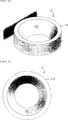
Die
Das Reflektorteil
Das Reflektorteil
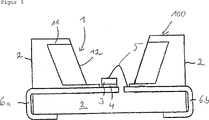
Die
Das Gehäuse
Das Gehäusematerial
Das Material für das Reflektorteil
Es ist aber auch möglich, dass der Schmelzpunkt des Reflektorteils
Das Reflektorteil
Das Gehäuse
Das Gehäusematerial
In das zweite Kunststoffmaterial können Füllstoffe zur Einstellung der optischen Eigenschaften und der mechanischen Stabilität wie Ruß, Pigmente und/oder Glasfasern eingebracht sein.In the second plastic material fillers for adjusting the optical properties and mechanical stability such as carbon black, pigments and / or glass fibers may be introduced.
Im Ausführungsbeispiel der
Im Unterschied dazu ist im Ausführungsbeispiel der
Die Erfindung ist nicht durch die Beschreibung anhand der Ausführungsbeispiele auf diese beschränkt. Vielmehr umfasst die Erfindung jedes neue Merkmal sowie jede Kombination von Merkmalen, was insbesondere jede Kombination von Merkmalen in den Patentansprüchen beinhaltet, auch wenn dieses Merkmal oder diese Kombination selbst nicht explizit in den Patentansprüchen oder Ausführungsbeispielen angegeben ist.The invention is not limited by the description based on the embodiments of these. Rather, the invention encompasses any novel feature as well as any combination of features, including in particular any combination of features in the claims, even if this feature or combination itself is not explicitly stated in the claims or exemplary embodiments.
ZITATE ENTHALTEN IN DER BESCHREIBUNG QUOTES INCLUDE IN THE DESCRIPTION
Diese Liste der vom Anmelder aufgeführten Dokumente wurde automatisiert erzeugt und ist ausschließlich zur besseren Information des Lesers aufgenommen. Die Liste ist nicht Bestandteil der deutschen Patent- bzw. Gebrauchsmusteranmeldung. Das DPMA übernimmt keinerlei Haftung für etwaige Fehler oder Auslassungen.This list of the documents listed by the applicant has been generated automatically and is included solely for the better information of the reader. The list is not part of the German patent or utility model application. The DPMA assumes no liability for any errors or omissions.
Zitierte PatentliteraturCited patent literature
- US 6624491 [0001] US 6624491 [0001]
Claims (15)
Priority Applications (7)
| Application Number | Priority Date | Filing Date | Title |
|---|---|---|---|
| DE102009058421A DE102009058421A1 (en) | 2009-12-16 | 2009-12-16 | Method for producing a housing for an optoelectronic semiconductor component, housing and optoelectronic semiconductor component |
| CN2010800577362A CN102668144A (en) | 2009-12-16 | 2010-11-17 | Method for producing a housing for an optoelectronic semiconductor component, housing, and optoelectronic semiconductor component |
| JP2012543566A JP2013514641A (en) | 2009-12-16 | 2010-11-17 | Optoelectronic semiconductor component housing manufacturing method, housing, and optoelectronic semiconductor component |
| PCT/EP2010/067705 WO2011082876A1 (en) | 2009-12-16 | 2010-11-17 | Method for producing a housing for an optoelectronic semiconductor component, housing, and optoelectronic semiconductor component |
| US13/513,784 US9331255B2 (en) | 2009-12-16 | 2010-11-17 | Housing that includes reflector part and housing material formed with plastic material |
| EP10788034A EP2513985A1 (en) | 2009-12-16 | 2010-11-17 | Method for producing a housing for an optoelectronic semiconductor component, housing, and optoelectronic semiconductor component |
| KR1020127018624A KR20120106808A (en) | 2009-12-16 | 2010-11-17 | Method for producing a housing for an optoelectronic semiconductor component, housing, and optoelectronic semiconductor component |
Applications Claiming Priority (1)
| Application Number | Priority Date | Filing Date | Title |
|---|---|---|---|
| DE102009058421A DE102009058421A1 (en) | 2009-12-16 | 2009-12-16 | Method for producing a housing for an optoelectronic semiconductor component, housing and optoelectronic semiconductor component |
Publications (1)
| Publication Number | Publication Date |
|---|---|
| DE102009058421A1 true DE102009058421A1 (en) | 2011-06-22 |
Family
ID=43608617
Family Applications (1)
| Application Number | Title | Priority Date | Filing Date |
|---|---|---|---|
| DE102009058421A Withdrawn DE102009058421A1 (en) | 2009-12-16 | 2009-12-16 | Method for producing a housing for an optoelectronic semiconductor component, housing and optoelectronic semiconductor component |
Country Status (7)
| Country | Link |
|---|---|
| US (1) | US9331255B2 (en) |
| EP (1) | EP2513985A1 (en) |
| JP (1) | JP2013514641A (en) |
| KR (1) | KR20120106808A (en) |
| CN (1) | CN102668144A (en) |
| DE (1) | DE102009058421A1 (en) |
| WO (1) | WO2011082876A1 (en) |
Families Citing this family (15)
| Publication number | Priority date | Publication date | Assignee | Title |
|---|---|---|---|---|
| USRE47444E1 (en) | 2011-11-17 | 2019-06-18 | Lumens Co., Ltd. | Light emitting device package and backlight unit comprising the same |
| CN103262269B (en) * | 2011-11-24 | 2018-06-19 | 惠州科锐半导体照明有限公司 | LED encapsulation piece |
| TW201432949A (en) * | 2013-02-05 | 2014-08-16 | Lextar Electronics Corp | Lighting module and manufacturing method thereof |
| KR20140141227A (en) * | 2013-05-31 | 2014-12-10 | 제일모직주식회사 | Polyamide-Based Resin Composition Having Excellent Reflectance and Discoloration Resistance |
| US9293670B2 (en) * | 2014-04-07 | 2016-03-22 | Crystal Is, Inc. | Ultraviolet light-emitting devices and methods |
| DE102014105839A1 (en) * | 2014-04-25 | 2015-10-29 | Osram Opto Semiconductors Gmbh | Optoelectronic component and method for producing an optoelectronic component |
| JP6671117B2 (en) * | 2014-07-08 | 2020-03-25 | エルジー イノテック カンパニー リミテッド | Light emitting device package |
| KR102252156B1 (en) * | 2014-07-08 | 2021-05-17 | 엘지이노텍 주식회사 | Light emitting device package |
| US10256383B2 (en) | 2015-06-01 | 2019-04-09 | Mitsubishi Electric Corporation | Light emitting device with dark area and greater reflectance light area, display unit, and image display device |
| WO2017138779A1 (en) * | 2016-02-12 | 2017-08-17 | 엘지이노텍(주) | Light emitting device package and lighting apparatus comprising same |
| KR102562091B1 (en) * | 2016-02-12 | 2023-08-02 | 쑤저우 레킨 세미컨덕터 컴퍼니 리미티드 | Light emitting device package |
| KR102509312B1 (en) * | 2016-02-24 | 2023-03-17 | 쑤저우 레킨 세미컨덕터 컴퍼니 리미티드 | Light emitting device package |
| DE102016103059A1 (en) * | 2016-02-22 | 2017-08-24 | Osram Opto Semiconductors Gmbh | Semiconductor device and method for manufacturing a semiconductor device |
| DE102016105243A1 (en) | 2016-03-21 | 2017-09-21 | Infineon Technologies Ag | Spatially Selective roughening of encapsulant to promote adhesion with a functional structure |
| CN112816071B (en) * | 2021-01-06 | 2021-12-28 | 国家卫星气象中心(国家空间天气监测预警中心) | Infrared channel radiation stability monitoring method based on cloud top height algorithm |
Citations (5)
| Publication number | Priority date | Publication date | Assignee | Title |
|---|---|---|---|---|
| US6624491B2 (en) | 1998-06-30 | 2003-09-23 | Osram Opto Semiconductors Gmbh & Co. | Diode housing |
| US20060157722A1 (en) * | 2004-12-03 | 2006-07-20 | Kabushiki Kaisha Toshiba | Semiconductor light emitting device |
| DE60209964T2 (en) * | 2001-06-15 | 2006-11-30 | Toyoda Gosei Co., Ltd. | Potting compound for a light emitting diode |
| US20070262336A1 (en) * | 2006-05-11 | 2007-11-15 | Hiroto Tamaki | Light emitting device |
| DE112006000694T5 (en) * | 2005-03-24 | 2008-02-07 | Kyocera Corp. | Housing for light emitting device, light emitting device and lighting device |
Family Cites Families (25)
| Publication number | Priority date | Publication date | Assignee | Title |
|---|---|---|---|---|
| DE19945133C2 (en) | 1999-09-21 | 2002-06-27 | Osram Opto Semiconductors Gmbh | Surface mount housing for detector components with side light sensitivity |
| CN1259732C (en) * | 2000-09-29 | 2006-06-14 | 欧姆龙株式会社 | Optical device for optical element and equipment using the same |
| JP4211359B2 (en) * | 2002-03-06 | 2009-01-21 | 日亜化学工業株式会社 | Manufacturing method of semiconductor device |
| WO2004001862A1 (en) | 2002-06-19 | 2003-12-31 | Sanken Electric Co., Ltd. | Semiconductor light emitting device, method for producing the same and reflector for semiconductor light emitting device |
| TWI292961B (en) * | 2002-09-05 | 2008-01-21 | Nichia Corp | Semiconductor device and an optical device using the semiconductor device |
| EP1597764A1 (en) * | 2003-02-28 | 2005-11-23 | Osram Opto Semiconductors GmbH | Optoelectronic component comprising a housing body which is metallised in a structured manner, method for producing one such component, and method for the structured metallisation of a body containing plastic |
| JP4182783B2 (en) * | 2003-03-14 | 2008-11-19 | 豊田合成株式会社 | LED package |
| DE10323857A1 (en) * | 2003-05-26 | 2005-01-27 | Osram Opto Semiconductors Gmbh | Housing for a laser diode device, laser diode device and method of manufacturing a laser diode device |
| DE10360943A1 (en) * | 2003-12-23 | 2005-07-21 | Engel, Hartmut S. | lighting device |
| JP2005243973A (en) * | 2004-02-26 | 2005-09-08 | Kyocera Corp | Light-emitting device and luminaire |
| DE102004053116A1 (en) * | 2004-11-03 | 2006-05-04 | Tridonic Optoelectronics Gmbh | Light-emitting diode arrangement with color conversion material |
| KR100580753B1 (en) * | 2004-12-17 | 2006-05-15 | 엘지이노텍 주식회사 | Light emitting device package |
| KR100631992B1 (en) * | 2005-07-19 | 2006-10-09 | 삼성전기주식회사 | Light emitting diode package having dual lens structure for laterally emitting light |
| CN101846247B (en) * | 2005-12-22 | 2013-04-17 | 松下电器产业株式会社 | Lighting apparatus with LED |
| WO2007146295A2 (en) * | 2006-06-13 | 2007-12-21 | Powerweb Technologies, Inc. | Led light pod with modular optics and heat dissipation structure |
| US8367945B2 (en) * | 2006-08-16 | 2013-02-05 | Cree Huizhou Opto Limited | Apparatus, system and method for use in mounting electronic elements |
| JP4846498B2 (en) * | 2006-09-22 | 2011-12-28 | 株式会社東芝 | Optical semiconductor device and method for manufacturing optical semiconductor device |
| DE102006046678A1 (en) * | 2006-09-29 | 2008-04-03 | Osram Opto Semiconductors Gmbh | Housing for use with semiconductor body of e.g. LED unit, has plastic-base body with plastic components, where one plastic component is made of material differing from that of other component in optical characteristic |
| KR100801621B1 (en) * | 2007-06-05 | 2008-02-11 | 서울반도체 주식회사 | Led package |
| JP2008305940A (en) * | 2007-06-07 | 2008-12-18 | Showa Denko Kk | Display, cap, light-emitting device, and manufacturing methods of same display, cap, and light-emitting device |
| US8118451B2 (en) * | 2008-03-13 | 2012-02-21 | Fraen Corporation | Reflective variable spot size lighting devices and systems |
| US20100032702A1 (en) * | 2008-08-11 | 2010-02-11 | E. I. Du Pont De Nemours And Company | Light-Emitting Diode Housing Comprising Fluoropolymer |
| DE102008038748B4 (en) | 2008-08-12 | 2022-08-04 | OSRAM Opto Semiconductors Gesellschaft mit beschränkter Haftung | Surface-mount optoelectronic semiconductor component |
| DE102009033287A1 (en) * | 2009-07-15 | 2011-01-20 | Osram Opto Semiconductors Gmbh | Light-emitting diode and method for producing a light-emitting diode |
| US8585253B2 (en) * | 2009-08-20 | 2013-11-19 | Illumitex, Inc. | System and method for color mixing lens array |
-
2009
- 2009-12-16 DE DE102009058421A patent/DE102009058421A1/en not_active Withdrawn
-
2010
- 2010-11-17 US US13/513,784 patent/US9331255B2/en not_active Expired - Fee Related
- 2010-11-17 CN CN2010800577362A patent/CN102668144A/en active Pending
- 2010-11-17 JP JP2012543566A patent/JP2013514641A/en not_active Withdrawn
- 2010-11-17 EP EP10788034A patent/EP2513985A1/en not_active Withdrawn
- 2010-11-17 WO PCT/EP2010/067705 patent/WO2011082876A1/en active Application Filing
- 2010-11-17 KR KR1020127018624A patent/KR20120106808A/en not_active Application Discontinuation
Patent Citations (5)
| Publication number | Priority date | Publication date | Assignee | Title |
|---|---|---|---|---|
| US6624491B2 (en) | 1998-06-30 | 2003-09-23 | Osram Opto Semiconductors Gmbh & Co. | Diode housing |
| DE60209964T2 (en) * | 2001-06-15 | 2006-11-30 | Toyoda Gosei Co., Ltd. | Potting compound for a light emitting diode |
| US20060157722A1 (en) * | 2004-12-03 | 2006-07-20 | Kabushiki Kaisha Toshiba | Semiconductor light emitting device |
| DE112006000694T5 (en) * | 2005-03-24 | 2008-02-07 | Kyocera Corp. | Housing for light emitting device, light emitting device and lighting device |
| US20070262336A1 (en) * | 2006-05-11 | 2007-11-15 | Hiroto Tamaki | Light emitting device |
Also Published As
| Publication number | Publication date |
|---|---|
| CN102668144A (en) | 2012-09-12 |
| EP2513985A1 (en) | 2012-10-24 |
| JP2013514641A (en) | 2013-04-25 |
| US9331255B2 (en) | 2016-05-03 |
| KR20120106808A (en) | 2012-09-26 |
| WO2011082876A1 (en) | 2011-07-14 |
| US20120280116A1 (en) | 2012-11-08 |
Similar Documents
| Publication | Publication Date | Title |
|---|---|---|
| DE102009058421A1 (en) | Method for producing a housing for an optoelectronic semiconductor component, housing and optoelectronic semiconductor component | |
| DE102009055786A1 (en) | Housing, optoelectronic component and method for producing a housing | |
| EP0852815B1 (en) | Process of manufacturing an optoelectronic semiconductor device | |
| EP1042819B1 (en) | Surface-mounted optoelectronic component and method for producing same | |
| DE102005036520A1 (en) | Optical component, optoelectronic component with the component and its manufacture | |
| DE102010028407A1 (en) | Optoelectronic component and method for producing an optoelectronic component | |
| DE102006046678A1 (en) | Housing for use with semiconductor body of e.g. LED unit, has plastic-base body with plastic components, where one plastic component is made of material differing from that of other component in optical characteristic | |
| DE102006002539A1 (en) | Manufacture of light emitting diode assembly involves providing base on lead frame, installing light emitting diode in base, treating lead frame with base, and over molding cover | |
| DE102009033287A1 (en) | Light-emitting diode and method for producing a light-emitting diode | |
| EP2989666B1 (en) | Optoelectronic component and method for the production thereof | |
| WO2016012189A1 (en) | Semiconductor lamp and method for producing same | |
| EP1699089A1 (en) | Method and mold for the manufacturing of an optical semiconductor modul | |
| WO2005064696A1 (en) | Radiation-emitting and/or radiation-receiving semiconductor component and method for the production thereof | |
| WO2007006378A1 (en) | Optoelectronic components comprising adhesive | |
| DE19940319B4 (en) | Process for low-tension placement of a lens on a surface-mountable optoelectronic component | |
| DE102008048846A1 (en) | Optoelectronic component | |
| DE102010013317A1 (en) | Optoelectronic component, housing for this and method for producing the optoelectronic component | |
| WO2017153585A1 (en) | Led module with silicon lenses | |
| DE102008044847A1 (en) | Optoelectronic component has support with electrically conductive lead frame, which has two elements, where organic layer is arranged on both elements | |
| DE10214119A1 (en) | Optoelectronic component comprises a casting compound which lets through radiation and consist of silicone or a silicone resin | |
| EP2067180A2 (en) | Optical element, radiation-emitting component and method for producing an optical element | |
| WO2017037036A1 (en) | Microlens for led module | |
| WO2012038164A1 (en) | Electronic component | |
| DE102011100028A1 (en) | Component and method for manufacturing a device | |
| DE3012523A1 (en) | Radiation-sensitive semiconductor element - embedded under filter glass disc in transparent plastic |
Legal Events
| Date | Code | Title | Description |
|---|---|---|---|
| R005 | Application deemed withdrawn due to failure to request examination |