KR20120106808A - Method for producing a housing for an optoelectronic semiconductor component, housing, and optoelectronic semiconductor component - Google Patents
Method for producing a housing for an optoelectronic semiconductor component, housing, and optoelectronic semiconductor component Download PDFInfo
- Publication number
- KR20120106808A KR20120106808A KR1020127018624A KR20127018624A KR20120106808A KR 20120106808 A KR20120106808 A KR 20120106808A KR 1020127018624 A KR1020127018624 A KR 1020127018624A KR 20127018624 A KR20127018624 A KR 20127018624A KR 20120106808 A KR20120106808 A KR 20120106808A
- Authority
- KR
- South Korea
- Prior art keywords
- housing
- reflector part
- semiconductor component
- optoelectronic semiconductor
- plastic material
- Prior art date
Links
Images

Classifications
-
- H—ELECTRICITY
- H01—ELECTRIC ELEMENTS
- H01L—SEMICONDUCTOR DEVICES NOT COVERED BY CLASS H10
- H01L33/00—Semiconductor devices with at least one potential-jump barrier or surface barrier specially adapted for light emission; Processes or apparatus specially adapted for the manufacture or treatment thereof or of parts thereof; Details thereof
- H01L33/48—Semiconductor devices with at least one potential-jump barrier or surface barrier specially adapted for light emission; Processes or apparatus specially adapted for the manufacture or treatment thereof or of parts thereof; Details thereof characterised by the semiconductor body packages
- H01L33/483—Containers
- H01L33/486—Containers adapted for surface mounting
-
- H—ELECTRICITY
- H01—ELECTRIC ELEMENTS
- H01L—SEMICONDUCTOR DEVICES NOT COVERED BY CLASS H10
- H01L33/00—Semiconductor devices with at least one potential-jump barrier or surface barrier specially adapted for light emission; Processes or apparatus specially adapted for the manufacture or treatment thereof or of parts thereof; Details thereof
- H01L33/48—Semiconductor devices with at least one potential-jump barrier or surface barrier specially adapted for light emission; Processes or apparatus specially adapted for the manufacture or treatment thereof or of parts thereof; Details thereof characterised by the semiconductor body packages
- H01L33/58—Optical field-shaping elements
- H01L33/60—Reflective elements
-
- H—ELECTRICITY
- H01—ELECTRIC ELEMENTS
- H01L—SEMICONDUCTOR DEVICES NOT COVERED BY CLASS H10
- H01L2224/00—Indexing scheme for arrangements for connecting or disconnecting semiconductor or solid-state bodies and methods related thereto as covered by H01L24/00
- H01L2224/01—Means for bonding being attached to, or being formed on, the surface to be connected, e.g. chip-to-package, die-attach, "first-level" interconnects; Manufacturing methods related thereto
- H01L2224/26—Layer connectors, e.g. plate connectors, solder or adhesive layers; Manufacturing methods related thereto
- H01L2224/31—Structure, shape, material or disposition of the layer connectors after the connecting process
- H01L2224/32—Structure, shape, material or disposition of the layer connectors after the connecting process of an individual layer connector
- H01L2224/321—Disposition
- H01L2224/32151—Disposition the layer connector connecting between a semiconductor or solid-state body and an item not being a semiconductor or solid-state body, e.g. chip-to-substrate, chip-to-passive
- H01L2224/32221—Disposition the layer connector connecting between a semiconductor or solid-state body and an item not being a semiconductor or solid-state body, e.g. chip-to-substrate, chip-to-passive the body and the item being stacked
- H01L2224/32245—Disposition the layer connector connecting between a semiconductor or solid-state body and an item not being a semiconductor or solid-state body, e.g. chip-to-substrate, chip-to-passive the body and the item being stacked the item being metallic
-
- H—ELECTRICITY
- H01—ELECTRIC ELEMENTS
- H01L—SEMICONDUCTOR DEVICES NOT COVERED BY CLASS H10
- H01L2224/00—Indexing scheme for arrangements for connecting or disconnecting semiconductor or solid-state bodies and methods related thereto as covered by H01L24/00
- H01L2224/01—Means for bonding being attached to, or being formed on, the surface to be connected, e.g. chip-to-package, die-attach, "first-level" interconnects; Manufacturing methods related thereto
- H01L2224/42—Wire connectors; Manufacturing methods related thereto
- H01L2224/47—Structure, shape, material or disposition of the wire connectors after the connecting process
- H01L2224/48—Structure, shape, material or disposition of the wire connectors after the connecting process of an individual wire connector
- H01L2224/4805—Shape
- H01L2224/4809—Loop shape
- H01L2224/48091—Arched
-
- H—ELECTRICITY
- H01—ELECTRIC ELEMENTS
- H01L—SEMICONDUCTOR DEVICES NOT COVERED BY CLASS H10
- H01L2224/00—Indexing scheme for arrangements for connecting or disconnecting semiconductor or solid-state bodies and methods related thereto as covered by H01L24/00
- H01L2224/01—Means for bonding being attached to, or being formed on, the surface to be connected, e.g. chip-to-package, die-attach, "first-level" interconnects; Manufacturing methods related thereto
- H01L2224/42—Wire connectors; Manufacturing methods related thereto
- H01L2224/47—Structure, shape, material or disposition of the wire connectors after the connecting process
- H01L2224/48—Structure, shape, material or disposition of the wire connectors after the connecting process of an individual wire connector
- H01L2224/481—Disposition
- H01L2224/48151—Connecting between a semiconductor or solid-state body and an item not being a semiconductor or solid-state body, e.g. chip-to-substrate, chip-to-passive
- H01L2224/48221—Connecting between a semiconductor or solid-state body and an item not being a semiconductor or solid-state body, e.g. chip-to-substrate, chip-to-passive the body and the item being stacked
- H01L2224/48245—Connecting between a semiconductor or solid-state body and an item not being a semiconductor or solid-state body, e.g. chip-to-substrate, chip-to-passive the body and the item being stacked the item being metallic
- H01L2224/48247—Connecting between a semiconductor or solid-state body and an item not being a semiconductor or solid-state body, e.g. chip-to-substrate, chip-to-passive the body and the item being stacked the item being metallic connecting the wire to a bond pad of the item
-
- H—ELECTRICITY
- H01—ELECTRIC ELEMENTS
- H01L—SEMICONDUCTOR DEVICES NOT COVERED BY CLASS H10
- H01L2224/00—Indexing scheme for arrangements for connecting or disconnecting semiconductor or solid-state bodies and methods related thereto as covered by H01L24/00
- H01L2224/73—Means for bonding being of different types provided for in two or more of groups H01L2224/10, H01L2224/18, H01L2224/26, H01L2224/34, H01L2224/42, H01L2224/50, H01L2224/63, H01L2224/71
- H01L2224/732—Location after the connecting process
- H01L2224/73251—Location after the connecting process on different surfaces
- H01L2224/73265—Layer and wire connectors
-
- H—ELECTRICITY
- H01—ELECTRIC ELEMENTS
- H01L—SEMICONDUCTOR DEVICES NOT COVERED BY CLASS H10
- H01L24/00—Arrangements for connecting or disconnecting semiconductor or solid-state bodies; Methods or apparatus related thereto
- H01L24/73—Means for bonding being of different types provided for in two or more of groups H01L24/10, H01L24/18, H01L24/26, H01L24/34, H01L24/42, H01L24/50, H01L24/63, H01L24/71
Abstract
본 발명은 광전자 반도체 컴포넌트(3)용 하우징(100)을 제조하기 위한 방법에 관한 것이며, 상기 방법에서는 조립식 반사기 파트(1)가 하우징 재료(2)에 의해 국부적으로 인케이싱(encasing)된다. 또한, 본 발명은 하우징(100) 및 광전자 반도체 컴포넌트와도 관련한다. The present invention relates to a method for manufacturing a housing (100) for an optoelectronic semiconductor component (3) in which the prefabricated reflector part (1) is locally encapsulated by the housing material (2). The invention also relates to the housing 100 and the optoelectronic semiconductor component.
Description
본 발명은 광전자 반도체 컴포넌트용 하우징을 제조하기 위한 방법에 관한 것이다. 상기 광전자 반도체 컴포넌트로는 예를 들어 발광 다이오드, 반도체 레이저 또는 광 검출기(photodetector)가 사용된다.The present invention relates to a method for manufacturing a housing for an optoelectronic semiconductor component. As the optoelectronic semiconductor component, for example, a light emitting diode, a semiconductor laser or a photodetector is used.
간행물 US 6,624,491호는 광전자 반도체 컴포넌트용 하우징을 기술하고 있다.Publication US 6,624,491 describes a housing for an optoelectronic semiconductor component.
본 발명의 해결 과제는 특히 노화에 저항력이 있는 광전자 반도체 컴포넌트용 하우징이 얻어지는 광전자 반도체 컴포넌트용 하우징을 제조하기 위한 방법을 제공하는 데 있다. The problem to be solved by the present invention is to provide a method for manufacturing a housing for an optoelectronic semiconductor component, in particular in which a housing for an optoelectronic semiconductor component resistant to aging is obtained.
본 발명에 따른 방법의 적어도 하나의 실시 예에 따르면, 상기 방법은 하우징의 반사기 파트가 제공되는 방법 단계를 포함한다. 다시 말해, 상기 반사기 파트는 조립식이며, 하우징의 다른 컴포넌트들과 함께 제조되지 않는다.According to at least one embodiment of the method according to the invention, the method comprises a method step in which a reflector part of a housing is provided. In other words, the reflector part is prefabricated and is not manufactured with the other components of the housing.
반사기 파트는 반도체 컴포넌트에서 생성된 전자기 방사선 또는 상기 반도체 컴포넌트로부터 수신된 전자기 방사선을 반사하기 위해 제공되어 있다. 다시 말해, 상기 반사기 파트는 상기 반도체 컴포넌트의 작동 중에 반사기 파트의 표면상으로 입사될 전자기 방사선을 반사한다. 이러한 목적을 위해 상기 반사기 파트는 전자기 방사선의 반사에 적합한 적어도 하나의 내부면을 갖는다. 그러한 경우 상기 전자기 방사선은 예를 들어 UV-방사선의 스펙트럼 범위에서 적외선의 스펙트럼 범위까지의 파장을 갖는 전자기 방사선이다. 반사기 파트는 예를 들어 횡단면에서 볼 때 링형으로 형성되어 있다. 이 경우, "링형으로"라는 의미는 반사기 파트가 횡단면에서 볼 때 원형의 링으로서만 형성되어야 한다는 것을 의미하지는 않으며, 오히려 반사기 파트는 원형, 타원형 또는 직사각형의 기본형태를 가질 수도 있다. 최종 광전자 반도체 컴포넌트에서 반사기 파트는 예를 들어 반도체 컴포넌트의 광전자 반도체 소자(예를 들어 발광 다이오드 칩)를 프레임 형태로 둘러싼다.The reflector part is provided for reflecting electromagnetic radiation generated in the semiconductor component or electromagnetic radiation received from the semiconductor component. In other words, the reflector part reflects electromagnetic radiation that will be incident on the surface of the reflector part during operation of the semiconductor component. For this purpose the reflector part has at least one inner surface which is suitable for the reflection of electromagnetic radiation. In such a case the electromagnetic radiation For example electromagnetic radiation having a wavelength from the spectral range of UV-radiation to the spectral range of infrared. The reflector part is formed in a ring shape, for example in cross section. In this case, the term "in a ring" does not mean that the reflector part should only be formed as a circular ring when viewed in cross section, but rather the reflector part may have a basic shape of round, oval or rectangular. In the final optoelectronic semiconductor component the reflector part surrounds, for example, the optoelectronic semiconductor element (eg a light emitting diode chip) of the semiconductor component in the form of a frame.
반사기 파트는 링형 반사기 파트의 개구쪽을 향하고 있는 적어도 하나의 내부면을 갖는다. 최종 광전자 반도체 컴포넌트에서는 상기 적어도 하나의 내부면은 예를 들어 반도체 컴포넌트의 광전자 반도체 소자(예를 들어 발광 다이오드 칩)쪽을 향하고 있다.The reflector part has at least one inner surface facing towards the opening of the ring reflector part. In the final optoelectronic semiconductor component the at least one inner surface is directed towards the optoelectronic semiconductor element (eg a light emitting diode chip) of the semiconductor component, for example.
본 발명에 따른 방법의 적어도 하나의 실시 예에 따르면, 상기 방법은 반사기 파트가 하우징 재료에 의해 인케이싱(encasing)되는 방법 단계를 포함한다. 이 경우, 상기 반사기 파트는 바람직하게 국부적으로만 인케이싱되고, 그 결과 예를 들어 반사기 파트의 상기 적어도 하나의 내부면의 부분들 또는 전체 내부면은 하우징 재료를 갖지 않는다. 인케이싱시, 상기 하우징 재료는 국부적으로 반사기 파트와 직접 접촉하게 되고, 이 경우 반사기 파트와 하우징 재료 간에는 기계적으로 견고한 결합이 형성된다. 그러한 경우, 반사기 파트와 하우징 재료를 분리하는 것은 파괴 없이는 가능하지 않은데, 다시 말해서, 상기 컴포넌트들 중에 하나의 컴포넌트 또는 두 개의 컴포넌트의 파괴를 통해서만 반사기 파트와 하우징 재료 간의 결합이 다시 분리될 수 있다.According to at least one embodiment of the method according to the invention, the method comprises a method step wherein the reflector part is encased by the housing material. In this case, the reflector part is preferably only locally encased so that, for example, parts or the entire inner surface of the at least one inner surface of the reflector part do not have a housing material. In encasing, the housing material is in direct contact with the reflector part locally, in which case a mechanically rigid bond is formed between the reflector part and the housing material. In such a case, it is not possible to separate the reflector part and the housing material without breaking, that is to say that the coupling between the reflector part and the housing material can only be separated again only by breaking one or two of the components.
이 경우 반사기 파트는 인케이싱 이전에 제공된다. 반사기 파트가 인케이싱 이전에 제공된다는 것은, 특히 상기 반사기 파트가 선행하는 제조 단계들에서 별도로 제조된 하우징의 조립식 컴포넌트라는 것을 의미한다. 그 때문에 반사기 파트로는 기계적으로 안정적이고 자력 지지되는 하우징 컴포넌트가 사용된다.In this case the reflector part is provided before encasing. The provision of the reflector part before the casing means that the reflector part is in particular a prefabricated component of the housing manufactured separately in the preceding manufacturing steps. For this reason, as the reflector part, a mechanically stable and magnetically supported housing component is used.
대안적으로 반사기 파트는 하우징 재료로 이루어진 하우징 기본 몸체의 제조 후, 하우징 기본 몸체상으로 압축되는 박막(folie)의 형태로 제공될 수도 있다.Alternatively, the reflector part may be provided in the form of a foil that is pressed onto the housing base body after manufacture of the housing base body made of the housing material.
본 발명에 따른 적어도 하나의 실시 예에 따르면, 반사기 파트를 하우징 재료에 의해 인케이싱하는 공정은 사출 성형 공정에 의해 제조된다. 다시 말해서, 하우징의 나머지 부분으로부터 분리되어 제조된 반사기 파트는 사출 성형 기계 내에 삽입되어 하우징 재료에 의해 압출된다. 이 경우, 반사기 파트의 내부면은 바람직하게 적어도 국부적으로 하우징 재료를 갖지 않는다.According to at least one embodiment according to the invention, the process of encapsulating the reflector part by the housing material is produced by an injection molding process. In other words, the reflector part manufactured separately from the rest of the housing is inserted into the injection molding machine and extruded by the housing material. In this case, the inner surface of the reflector part preferably does not have a housing material at least locally.
본 발명에 따른 방법의 적어도 하나의 실시 예에 따르면, 반사기 파트는 제 1 플라스틱 재료에 의해 형성되어 있고, 하우징 재료는 제 2 플라스틱 재료에 의해 형성되어 있다. 이 경우, 반사기 파트가 제 1 플라스틱 재료로 이루어지거나, 또는 제 1 플라스틱 재료가 추가의 혼합물들 및 충전재들을 위한 매트릭스 재료로서 사용되는 것도 가능하다. 하우징 재료 또한 제 2 플라스틱 재료로 이루어지거나 또는 추가의 혼합물들 및 충전재들을 위한 매트릭스 재료로서 사용될 수 있다. 이 경우 상기 제 1 및 제 2 플라스틱 재료는 서로 상이하며, 상기 제 1 및 제 2 플라스틱 재료는 바람직하게 하기의 재료 특성들 중 적어도 하나의 재료 특성과 관련하여 구별된다: 온도 내성(temperature resistance), 전자기 방사선에 대한 내성.According to at least one embodiment of the method according to the invention, the reflector part is formed by the first plastic material and the housing material is formed by the second plastic material. In this case, it is also possible for the reflector part to consist of the first plastic material, or the first plastic material to be used as the matrix material for further mixtures and fillers. The housing material may also be made of a second plastic material or used as matrix material for further mixtures and fillers. In this case the first and second plastic materials are different from one another, and the first and second plastic materials are preferably distinguished in relation to at least one of the following material properties: temperature resistance, Resistance to electromagnetic radiation.
이 경우, 온도 내성이란 특히 하기의 사항을 의미한다: 상대적으로 더 강한 온도 내성을 갖는 플라스틱 재료는 특히 상대적으로 더 약한 온도 내성을 갖는 플라스틱 재료보다 상대적으로 더 높은 한계 온도에서부터 비로소 변색, 변형 또는 파괴되는 특징을 갖는다. 대안적으로 또는 추가적으로 상대적으로 더 강한 온도 내성을 갖는 플라스틱 재료는 상대적으로 더 약한 온도 내성을 갖는 재료보다 주어진 온도에서의 변형, 변색 또는 파괴에 대해 상대적으로 더 긴 시간을 견뎌낼 수 있다.In this case, temperature resistance means especially the following: A plastic material with a relatively higher temperature resistance does not discolor, deform or break down, especially at a relatively higher limit temperature than a plastic material with a relatively weak temperature resistance. It is characterized by. Alternatively or additionally, plastic materials with relatively stronger temperature resistance can withstand relatively longer times against deformation, discoloration or destruction at a given temperature than materials with relatively weaker temperature resistance.
전자기 방사선에 대한 내성이란 특히 하기의 사항을 의미한다: 전자기 방사선에 대해 상대적으로 더 강한 내성을 갖는 플라스틱 재료와 전자기 방사선에 대해 상대적으로 더 약한 내성을 갖는 플라스틱 재료를 전자기 방사선에 노출했을 때, 전자기 방사선에 대해 상대적으로 더 강한 내성을 갖는 재료는 전자기 방사선에 대해 상대적으로 더 약한 내성을 갖는 재료보다 시간상으로 더 나중에 변형되거나 변색된다. 전자기 방사선으로는 예를 들어 UV-방사선 또는 청색 광의 파장 범위에서 나오는 전자기 방사선이 사용된다. 특히 전자기 방사선에 대해 상대적으로 더 작은 내성을 갖는 재료와 비교해서 전자기 방사선에 대해 상대적으로 더 큰 내성을 갖는 플라스틱 재료의 변색은 더 더디게 시작된다.Immunity to electromagnetic radiation means especially the following: When exposed to electromagnetic radiation, a plastic material having a relatively higher resistance to electromagnetic radiation and a plastic material having a relatively weaker resistance to electromagnetic radiation is exposed to electromagnetic radiation. Materials that have a relatively stronger resistance to radiation deform or discolor later in time than materials that have a relatively weaker resistance to electromagnetic radiation. As electromagnetic radiation, for example, electromagnetic radiation coming from the wavelength range of UV-radiation or blue light is used. In particular, discoloration of plastic materials having a relatively higher resistance to electromagnetic radiation starts slower compared to materials having a relatively smaller resistance to electromagnetic radiation.
본 발명에 따른 방법의 적어도 하나의 실시 예에 따르면, 상기 방법은 하기의 단계들을 포함한다:According to at least one embodiment of the method according to the invention, the method comprises the following steps:
A. 전자기 방사선의 반사에 적합한 적어도 하나의 내부면을 갖는 반사기 파트를 제공하는 단계,A. providing a reflector part having at least one inner surface suitable for reflection of electromagnetic radiation,
B. 상기 반사기 파트를 하우징 재료에 의해 국부적으로 인케이싱하는 단계.B. locally encasing the reflector part by a housing material.
이 경우, 상기 인케이싱 공정은 사출 성형 공정에 의해 실행되고, 반사기 파트의 내부면은 적어도 국부적으로 하우징 재료를 갖지 않으며, 상기 반사기 파트는 제 1 플라스틱 재료에 의해 형성되어 있고, 상기 하우징 재료는 제 2 플라스틱 재료에 의해 형성되며, 상기 제 1 플라스틱 재료는 상기 제 2 플라스틱 재료와는 상이하고, 상기 제 1 플라스틱 재료와 상기 제 2 플라스틱 재료는 하기의 재료 특성들 중 적어도 하나의 재료 특성에 있어서 서로 구별된다: 온도 내성, 전자기 방사선에 대한 내성.In this case, the encasing process is performed by an injection molding process, the inner surface of the reflector part does not have at least locally a housing material, the reflector part is formed by a first plastic material, and the
가격이 저렴한 기본 재료가 종종 광전자 반도체 컴포넌트들 내에서 열 및/또는 전자기 방사선에 의한 재료의 부하로 인해 노화된다는 인식은 특히 본 발명에 따른 방법의 기초가 된다. 특히 - 예를 들어 반사기 파트와 같은 - 하우징의 광학 컴포넌트들의 노화의 경우에는, 이러한 광학 컴포넌트들의 노화 현상이 광전자 반도체 컴포넌트의 수명을 상당히 단축시킬 수 있다. 본 발명에서는 반사기 파트와 하우징 재료만 서로 분리되어 제조되는데, 그럼으로써 하우징 컴포넌트들을 위한 재료의 선택이 간소화되며, 전체 하우징을 일체형으로 형성하기 위해서는 비용이 상당히 높을 수 있거나 또는 온도 내성 및/또는 전자기 방사선에 대한 내성에 있어서의 요건들을 충족시키지 않는 플라스틱 재료들이 서로 조합될 수 있다. The recognition that inexpensive base materials are often aging due to the loading of the material by heat and / or electromagnetic radiation in optoelectronic semiconductor components is in particular the basis of the method according to the invention. Especially in the case of aging of optical components of the housing-for example, reflector parts-the aging phenomenon of such optical components can significantly shorten the life of the optoelectronic semiconductor component. In the present invention, only the reflector part and the housing material are manufactured separately from each other, which simplifies the selection of the materials for the housing components, which can be quite expensive in order to form the whole housing in one piece or with temperature tolerance and / or electromagnetic radiation. Plastic materials that do not meet the requirements for resistance to can be combined with each other.
또한, 본 발명에서는 광전자 반도체 컴포넌트용 하우징이 제시된다. 상기 하우징은 본 발명에 기술된 방법에 의해 제조될 수 있다. 다시 말해서, 본 발명의 방법을 위해 공개된 전체 특징들은 상기 하우징을 위해서도 공개되며, 그 반대로도 가능하다.In addition, the present invention provides a housing for an optoelectronic semiconductor component. The housing can be manufactured by the method described in the present invention. In other words, all the features disclosed for the method of the invention are also disclosed for the housing and vice versa.
본 발명에 따른 하우징의 적어도 하나의 실시 예에 따르면, 상기 하우징은 전자기 방사선의 반사에 적합한 적어도 하나의 내부면을 갖는 반사기 파트를 포함한다. 또한, 상기 하우징은 적어도 국부적으로 상기 반사기 파트의 표면과 직접 접촉해 있는 하우징 재료를 포함하며, 이 경우 반사기 파트와 하우징 재료는 결합 수단 없이 서로 기계적으로 결합되어 있다. 다시 말해, 상기 하우징 재료는 접착제 또는 예를 들어 프레스 끼워 맞춤(press fit)과 같이 육안으로 보이는(macroscopic) 기계적 결합에 의해 반사기 파트와 결합되어 있지 않고, 반사기 파트의 표면과 직접 접촉하여 반사기 파트의 재료와 긴밀한 결합을 형성한다.According to at least one embodiment of the housing according to the invention, the housing comprises a reflector part having at least one inner surface suitable for reflection of electromagnetic radiation. In addition, the housing comprises a housing material which is at least locally in direct contact with the surface of the reflector part, in which case the reflector part and the housing material are mechanically coupled to one another without coupling means. In other words, the housing material is not bonded to the reflector part by adhesive or macroscopic mechanical coupling, such as, for example, press fit, but is in direct contact with the surface of the reflector part, Forms a tight bond with the material.
이 경우 예를 들어 하우징 재료는 사출 성형 공정에 의해 반사기 파트와 기계적으로 결합될 수 있다. "사출 성형 공정"의 특징은 객관적인 특징인데, 그 이유는 사출 성형 공정에 의한 결합은 최종 컴포넌트에 캐스팅-심(casting-seam) 또는 사출 성형 노즐의 분리 흔적과 같이 상기 공정에 있어서 전형적인 흔적들로 인해 다른 결합 기술들로부터 입증될 수 있기 때문이다. 다시 말해서, 상기 컴포넌트는 사출 성형 공정의 흔적들을 갖는다.In this case, for example, the housing material may be mechanically coupled with the reflector part by an injection molding process. The characteristic of the "injection molding process" is an objective feature, since the bonding by the injection molding process is typical of the traces in the process, such as the separation traces of the casting-seam or injection molding nozzles in the final component. Because it can be proved from other coupling techniques. In other words, the component has traces of the injection molding process.
본 발명에 따른 하우징의 적어도 하나의 실시 예에 따르면, 이 경우 반사기 파트의 내부면은 적어도 부분적으로 하우징 재료를 갖지 않는다. 상기 반사기 파트의 내부면은 상기 내부면에 입사되는 전자기 방사선을 반사하는 광학적 작용을 하는 반사기 파트의 컴포넌트이다. 예를 들어 반사기 파트의 전체 내부면이 하우징 재료를 갖지 않을 수도 있다.According to at least one embodiment of the housing according to the invention, the inner surface of the reflector part in this case at least partially does not have a housing material. The inner surface of the reflector part is a component of the reflector part having an optical action of reflecting electromagnetic radiation incident on the inner surface. For example, the entire inner surface of the reflector part may not have a housing material.
본 발명에 따른 하우징의 적어도 하나의 실시 예에 따르면, 반사기 파트는 제 1 플라스틱 재료로 형성되어 있고, 하우징 재료는 제 2 플라스틱 재료로 형성되어 있으며, 이 경우 상기 제 1 플라스틱 재료는 상기 제 2 플라스틱 재료와는 상이하고, 상기 제 1 플라스틱 재료와 상기 제 2 플라스틱 재료는 하기 재료 특성들 중 적어도 하나의 특성과 관련하여 구별된다: 온도 내성, 전자기 방사선에 대한 내성.According to at least one embodiment of the housing according to the invention, the reflector part is formed of a first plastic material, the housing material is formed of a second plastic material, in which case the first plastic material is the second plastic Different from the material, the first plastic material and the second plastic material are distinguished with respect to at least one of the following material properties: temperature resistance, resistance to electromagnetic radiation.
광전자 반도체 컴포넌트용 하우징의 적어도 하나의 실시 예에 따르면, 상기 하우징은 전자기 방사선의 반사에 적합한 적어도 하나의 내부면을 갖는 반사기 파트를 포함하고, 상기 하우징은 또한 적어도 국부적으로 반사기 파트의 표면과 직접 접촉해 있는 하우징 재료를 포함한다. 이 경우 반사기 파트와 하우징 재료는 결합 수단 없이 기계적으로 서로 결합되어 있고, 상기 반사기 파트의 내부면은 적어도 국부적으로 하우징 재료를 갖지 않으며, 상기 반사기 파트는 제 1 플라스틱 재료로 형성되어 있고, 상기 하우징 재료는 제 2 플라스틱 재료로 형성되어 있으며, 이 경우 상기 제 1 플라스틱 재료는 상기 제 2 플라스틱 재료와는 상이하고, 상기 제 1 플라스틱 재료와 상기 제 2 플라스틱 재료는 하기의 재료 특성들 중 적어도 하나의 특성과 관련하여 구별된다: 온도 내성, 전자기 방사선에 대한 내성.According to at least one embodiment of a housing for an optoelectronic semiconductor component, the housing comprises a reflector part having at least one inner surface suitable for reflection of electromagnetic radiation, the housing also at least locally in direct contact with the surface of the reflector part. Housing material. In this case the reflector part and the housing material are mechanically joined together without a coupling means, the inner surface of the reflector part has at least locally no housing material, the reflector part is formed of a first plastic material and the housing material Is formed of a second plastic material, in which case the first plastic material is different from the second plastic material, and the first plastic material and the second plastic material are at least one of the following material properties. In connection with: temperature resistance, resistance to electromagnetic radiation.
하기에서는 각각 본 발명에 따른 방법뿐만 아니라 하우징에도 관련되는 하우징 및 하우징을 제조하기 위한 방법의 실시 예들이 기술되어 있다.In the following, embodiments of a housing and a method for manufacturing the housing are described which are respectively related to the housing as well as the method according to the invention.
본 발명에 따른 적어도 하나의 실시 예에 따르면, 하우징 재료는 하우징의 상부면에서 반사기 파트와 같은 높이에서 종료되거나 또는 상기 하우징 재료는 하우징의 상부면에서 반사기 파트 위로 돌출한다. 그러한 경우, 특히 하우징 재료 위로 반사기 파트가 돌출하지는 않는다.According to at least one embodiment according to the invention, the housing material terminates at the same height as the reflector part on the upper surface of the housing or the housing material projects above the reflector part on the upper surface of the housing. In such a case, in particular, the reflector part does not protrude above the housing material.
본 발명에 따른 적어도 하나의 실시 예에 따르면, 반사기 파트는 전적으로 사출 성형 공정에 의해 하우징 재료와 기계적으로 결합되어 있다. 이 경우 반사기 파트와 하우징 재료는 서로 바로 인접한다.According to at least one embodiment according to the invention, the reflector part is mechanically coupled with the housing material entirely by an injection molding process. In this case the reflector part and the housing material are immediately adjacent to each other.
특히 반사기 파트가 전적으로 하우징 재료와만 직접 접촉해 있는 것도 가능하다. 그러한 경우 상기 반사기 파트는 예를 들어 기판 또는 접속 지점들과 같은 하우징의 다른 컴포넌트들과는 접촉하지 않는다. 상기와 같은 방식으로 하우징 재료와 반사기 파트가 서로 특히 큰 면적의 접촉면을 가질 수도 있다.In particular, it is also possible for the reflector part to be in direct contact with the housing material entirely. In that case the reflector part is not in contact with other components of the housing, such as for example a substrate or connection points. In this way the housing material and the reflector part may have a particularly large area of contact with each other.
본 발명에 따른 적어도 하나의 실시 예에 따르면, 반사기 파트를 제공하기 이전에 상기 반사기 파트는 형상 절삭(shape cutting)에 의해 제조된다. 이 경우 형상 절삭 또는 절삭은 불필요한 재료가 연마의 형태로 제거되어, 재료가 원하는 형태로 제공되는 공정을 의미한다. 이 경우 형상 절삭 또한 최종 대상에서 예를 들어 사출 성형과 같은 다른 제조 공정들로부터 구별 가능한 객관적인 특징이다. 특히 제 1 플라스틱 재료가 예를 들어 폴리테트라플루오르에틸렌(PTFE)과 같은 플루오르폴리머인 반사기 파트는 형상 절삭에 우수하게 적합하다.According to at least one embodiment according to the invention, the reflector part is manufactured by shape cutting prior to providing the reflector part. In this case, shape cutting or cutting refers to a process in which unnecessary material is removed in the form of polishing, so that the material is provided in a desired shape. Shape cutting in this case is also an objective feature that can be distinguished from other manufacturing processes such as, for example, injection molding in the final object. In particular, reflector parts, in which the first plastic material is a fluoropolymer such as, for example, polytetrafluoroethylene (PTFE), are excellently suitable for shape cutting.
대안적으로 반사기 파트는 박막 쉘들(folie shells)에 의해 제조될 수도 있다. 박막 쉘에 의한 제조는 반사기 파트로서 박막이 사용되는 경우이다.Alternatively, the reflector part may be manufactured by thin shells. Manufacturing by thin film shells is when thin films are used as reflector parts.
본 발명에 따른 적어도 하나의 실시 예에 따르면, 반사기 파트는 제공되기 이전에 사출 성형 공정에 의해 제조된다. 상기 목적을 위해 하기 플라스틱들 중 적어도 하나의 플라스틱을 포함하거나 또는 하기 플라스틱들 중 적어도 하나의 플라스틱으로 이루어진 제 1 플라스틱 재료가 특히 우수하게 적합하다: 폴리부틸렌테레프탈레이트(PBT), 폴리에틸렌테레프탈레이트(PET), 폴리시클로헥실렌디메틸렌테레프탈레이트(PCT), 폴리에테르이미드(PEI), 액상결정폴리머(LCP), 고온-폴리아미드(HT-PA), 폴리에테르케톤(PEEK), 실리콘.According to at least one embodiment according to the invention, the reflector part is manufactured by an injection molding process before it is provided. Particularly well suited for this purpose are first plastic materials comprising or consisting of at least one of the following plastics: polybutylene terephthalate (PBT), polyethylene terephthalate ( PET), polycyclohexylenedimethylene terephthalate (PCT), polyetherimide (PEI), liquid crystalline polymer (LCP), high temperature-polyamide (HT-PA), polyetherketone (PEEK), silicone.
다시 말해서, 본 발명에 따른 제 1 실시 예에 따르면, 제 1 플라스틱 재료는 하기 재료들 중 적어도 하나의 재료를 포함하는 그룹으로부터 선택되어 있다: 폴리에스테르, 플루오르폴리머, 폴리에테르케톤, 폴리에테르이미드, 고온-폴리아미드, 폴리에테르케톤, 액상결정폴리머, 실리콘.In other words, according to a first embodiment according to the invention, the first plastic material is selected from the group comprising at least one of the following materials: polyester, fluoropolymer, polyetherketone, polyetherimide, Hot-polyamides, polyetherketones, liquid crystalline polymers, silicones.
본 발명에 따른 적어도 하나의 실시 예에 따르면, 제 2 플라스틱 재료는 하기 재료들 중 적어도 하나의 재료를 포함하는 그룹으로부터 선택되어 있다: 폴리아미드, 폴리페닐술피드, 폴리에테르이미드, 폴리페닐술폰.According to at least one embodiment according to the invention, the second plastic material is selected from the group comprising at least one of the following materials: polyamide, polyphenylsulfide, polyetherimide, polyphenylsulfone.
이 경우, 상기 제 1 플라스틱 재료는 특히 전자기 방사선에 대해 내성을 갖는 것을 특징으로 한다. 그러한 경우 특히 상기 제 1 플라스틱 재료는 상기 제 2 플라스틱 재료보다 전자기 방사선에 대해 더 강한 내성을 갖는다.In this case, the first plastic material is characterized in particular as being resistant to electromagnetic radiation. In such a case in particular the first plastic material has a stronger resistance to electromagnetic radiation than the second plastic material.
이 경우, 제 1 플라스틱 재료는 또한 제 2 플라스틱 재료보다 더 강한 온도 내성을 가질 수 있다. 하지만, 광전자 컴포넌트가 예를 들어 납땜 공정에 의한 장착을 위해 제공되는 경우에는, 바람직하게 하우징 재료를 구성하는 상기 제 2 플라스틱 재료는 특히 온도 내성을 갖도록 선택되며, 그 결과 제 2 플라스틱 재료가 제 1 플라스틱 재료보다 더 강한 온도 내성을 가질 수 있다.In this case, the first plastic material may also have stronger temperature resistance than the second plastic material. However, in the case where the optoelectronic component is provided for mounting by, for example, a soldering process, the second plastic material constituting the housing material is preferably selected to be particularly temperature resistant, so that the second plastic material is firstly selected. It can have stronger temperature resistance than plastic materials.
본 발명에 따른 적어도 하나의 실시 예에 따르면, 반사기 파트를 하우징 재료에 의해 내부면의 적어도 부분들까지 인케이싱하는 경우, 반사기 파트의 전체 표면은 하우징 재료에 의해 덮인다. 다시 말해서, 반사기 파트의 광학적 특성들이 부정적 영향을 받는 것 없이, 반사기 파트와 하우징 재료 간의 결합면은 바람직하게 특히 크게 선택된다. 상기와 같이 크게 선택된 결합면은 반사기 파트와 하우징 재료 간의 특히 우수한 접착을 가능하게 한다.According to at least one embodiment according to the invention, when the reflector part is encased by the housing material to at least parts of the inner surface, the entire surface of the reflector part is covered by the housing material. In other words, the bonding surface between the reflector part and the housing material is preferably chosen particularly large, without the optical properties of the reflector part being negatively affected. The largely chosen engagement surface as above allows particularly good adhesion between the reflector part and the housing material.
반사기 파트는 또한 하우징 재료로부터 반사기 파트의 잠재적인 분리를 저지하는 예를 들어 언더커트(undercut)와 같은 적어도 하나의 기계적 고정 구조를 추가로 가질 수 있다.The reflector part may further have at least one mechanical fixation structure such as, for example, an undercut that prevents potential detachment of the reflector part from the housing material.
본 발명에 따른 적어도 하나의 실시 예에 따르면, 하우징 재료와 반사기 파트는 자신들의 광학 특성들과 관련하여 구별된다. 예를 들어 상기 반사기 파트는 UV-방사선과 적외선 사이의 스펙트럼 범위에 놓인 전자기 방사선에 대하여 반사성으로 형성되어 있다. 그러한 경우 반사기 파트는 상기 스펙트럼 범위에서 나온 적어도 하나의 파장에 대해 적어도 80%, 바람직하게 적어도 90%의 반사율을 가질 수 있다. 그와 반대로 하우징 재료는 방사선 비투과성(예를 들어 유색), 방사선 흡수성(흑색)으로 형성될 수 있거나 또는 반사기 파트보다는 덜 강한 반사성으로 형성될 수 있다. 이 경우 하우징 재료와 반사기 파트의 광학적 특성들은 상응하는 혼합물들에 의해 제 1 또는 제 2 플라스틱 재료 내로 도달될 수 있다.According to at least one embodiment according to the invention, the housing material and the reflector part are distinguished in terms of their optical properties. For example, the reflector part is formed reflective to electromagnetic radiation that lies in the spectral range between UV-radiation and infrared radiation. In such a case the reflector part may have a reflectance of at least 80%, preferably at least 90% for at least one wavelength coming from said spectral range. In contrast, the housing material may be formed to be radiopaque (eg colored), radiation absorbing (black) or less reflective than the reflector part. In this case the optical properties of the housing material and the reflector part can be reached into the first or second plastic material by corresponding mixtures.
본 발명에 따른 적어도 하나의 실시 예에 따르면, 반사기 파트는 제 1 플라스틱 재료와 상기 플라스틱 재료 내로 삽입되어 있는 백색 염료를 포함한다. 백색 염료로는 예를 들어 하기의 재료들 중 적어도 하나의 재료가 사용된다: 티탄옥사이드, 리토폰, 바륨술페이트, 징크옥사이드, 징크술피드, 지르코늄디옥사이드, 석고가루(gesso). 백색 염료에 추가로 상기 제 1 플라스틱 재료는 예를 들어 반사기 파트의 기계적 안정성을 상승시키는 유리 섬유들과 같은 추가의 충전재들을 포함할 수 있다.According to at least one embodiment according to the invention, the reflector part comprises a first plastic material and a white dye inserted into the plastic material. As the white dye, for example, at least one of the following materials is used: titanium oxide, lithopone, barium sulfate, zinc oxide, zinc sulfide, zirconium dioxide, gypsum (gesso). In addition to the white dye, the first plastic material may comprise additional fillers such as, for example, glass fibers that increase the mechanical stability of the reflector part.
즉, 전체적으로 하우징 컴포넌트들의 기계적, 광학적 그리고 광화학적인 특성들이 간단한 방법으로 각각의 사용 조건들에 매칭되는 하우징이 구현될 수 있다.That is, a housing can be implemented in which the mechanical, optical and photochemical properties of the housing components as a whole are matched to the respective use conditions in a simple manner.
또한, 본 발명에는 광전자 컴포넌트가 제시되어 있다. 상기 광전자 컴포넌트는 본 발명에 기술되어 있는 것과 같은 하우징을 포함한다. 다시 말해서, 상기 하우징에 대해 공개되어 있는 모든 특징들은 광전자 컴포넌트에 대해서도 공개되어 있다. 또한, 상기 광전자 컴포넌트는 예를 들어 방사선 방출 반도체 칩과 같은 광전자 소자를 포함한다. 상기 방사선 방출 반도체 칩으로는 예를 들어 발광 다이오드 칩 또는 레이저 다이오드가 사용될 수 있다.Also present in the present invention is an optoelectronic component. The optoelectronic component includes a housing as described herein. In other words, all features disclosed for the housing are also disclosed for the optoelectronic component. The optoelectronic component also includes an optoelectronic device, for example a radiation emitting semiconductor chip. For example, a light emitting diode chip or a laser diode may be used as the radiation emitting semiconductor chip.
이 경우 상기 적어도 하나의 광전자 소자는 상기 소자가 반사기 파트의 상기 적어도 하나의 내부면에 의해 측면으로 둘러싸여 있도록 하우징 내로 삽입되어 있다. 다시 말해서, 상기 반사기 파트에 의해 리세스가 하우징 내에 형성되어 있고, 상기 리세스는 반사기 파트의 상기 적어도 하나의 내부면에 의해 측면으로 경계 지어져 있다. 상기 리세스 내로는 광전자 소자가 삽입되어 있다. 광전자 소자로부터 작동 중에 생성된 전자기 방사선은 반사기 파트의 상기 적어도 하나의 내부면으로 입사될 수 있고 상기 반사기 파트의 적어도 하나의 내부면으로부터 - 내부면의 형성에 따라 - 지향성 또는 확산성으로 반사된다.In this case the at least one optoelectronic device is inserted into the housing such that the device is laterally surrounded by the at least one inner surface of the reflector part. In other words, a recess is formed in the housing by the reflector part, the recess being laterally bounded by the at least one inner surface of the reflector part. An optoelectronic device is inserted into the recess. Electromagnetic radiation generated during operation from the optoelectronic device can be incident on the at least one inner surface of the reflector part and is reflected directionally or diffusely from the at least one inner surface of the reflector part-depending on the formation of the inner surface.
하기에서는 본 발명에 기술된 광전자 반도체 컴포넌트용 하우징 제조 방법, 본 발명에 기술된 하우징 그리고 본 발명에 기술된 광전자 반도체 컴포넌트가 실시 예들과 해당 도면들을 참조하여 더 자세히 설명된다.In the following, the housing manufacturing method for the optoelectronic semiconductor component described in the present invention, the housing described in the present invention and the optoelectronic semiconductor component described in the present invention are described in more detail with reference to the embodiments and the corresponding drawings.
도 1a 및 도 1b는 개략도를 참조하여 본 발명에 기술된 하우징의 실시 예에 대한 반사기 파트를 보여준다.
도 2a, 도 2b 및 도 3은 개략도를 참조하여 본 발명에 기술된 하우징들의 실시 예들과 함께 본 발명에 기술된 컴포넌트들의 실시 예들을 보여준다.1A and 1B show reflector parts for an embodiment of a housing described herein with reference to schematic diagrams.
2A, 2B and 3 show embodiments of the components described herein along with embodiments of the housings described herein with reference to schematic diagrams.
도면들에서 동일한, 동일한 형태의 또는 동일하게 작용하는 소자들에는 동일한 도면 부호들이 제공되었다. 도면들 그리고 상기 도면들에 도시된 소자들의 상호 크기 비율들은 척도에 맞는 것으로 간주될 수 없다. 오히려 개별 소자들은 더 나은 개관을 위하여 그리고/또는 더 나은 이해를 위하여 과도하게 크게 도시되어 있을 수 있다.In the figures the same reference numerals have been provided to identical, identically shaped or identically acting elements. The drawings and the mutual size ratios of the elements shown in the figures cannot be considered to be a measure. Rather, individual elements may be shown excessively large for a better overview and / or for a better understanding.
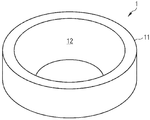
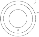
도 1a는 개략적인 사시도로 본 발명에 기술된 하우징의 실시 예를 위한 반사기 파트를 보여준다. 상기 반사기 파트는 도 1b에서는 평면도로 도시되어 있다. 반사기 파트(1)는 링형으로 형성되어 있다. 반사기 파트(1)는 내부면(12)을 포함하는 표면(11)을 갖는다. 내부면(12)은 전자기 방사선에 대하여 반사성으로 형성되어 있다.1A shows a reflector part for an embodiment of a housing described herein in a schematic perspective view. The reflector part is shown in plan view in FIG. 1B. The
방사선을 반사하는 반사기 파트(1)의 특성들을 향상시키기 위해 반사기 파트(1)는 백색 염료가 삽입되어 있는 본 발명에 기술된 제 1 플라스틱 재료로 이루어져 있다.In order to improve the properties of the
반사기 파트(1)는 예를 들어 형상 절삭 또는 사출 성형 공정에 의해 하우징의 나머지 부분과 별도로 제조되어 있다. 반사기 파트(1)는 기계적으로 자력 지지되는 경성의 하우징 컴포넌트이며, 상기 컴포넌트는 본 발명에 기술된 제조 공정에 의해 하우징의 나머지 컴포넌트들과 기계적으로 견고하게 결합되어 있다.The
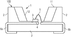
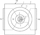
도 2a는 개략적인 단면도로 본 발명에 기술된 하우징(100)을 갖는 본 발명에 기술된 광전자 반도체 컴포넌트의 제 1 실시 예를 보여주고, 도 2b는 이와 관련된 평면도이다.FIG. 2A shows a first embodiment of an optoelectronic semiconductor component described in the present invention having a
하우징(100)은, 예를 들어 도 1a 및 도 1b와 연관하여 더 자세히 설명되어 있는 것과 같이, 반사기 파트(1)를 포함한다. 반사기 파트(1)의 표면(11)은 국부적으로 하우징 재료(2)와 직접 접촉해 있다.The
하우징 재료(2)는 사출 성형 공정에 의해 반사기 파트(1)에 접하여 스플레시(splash)되어 있고, 그 때문에 국부적으로 반사기 파트(1)와 직접 접촉해 있다. 다시 말해, 하우징 재료(2)는 반사기 파트(1)와 결합 수단 없이 결합되어 있다. 본 발명에서는 반사기 파트(1)의 전체 내부면(12)은 하우징 재료(2)를 갖지 않거나 또는 대체적으로 하우징 재료(2)를 갖지 않는다. 대체적으로 하우징 재료(2)를 갖지 않는다는 표현은 예를 들어 반사기 파트(1)의 내부면(12)이 면적비율에 대해 최대 10%, 특히 최대 5%로 하우징 재료(2)에 의해 덮일 수 있다는 것을 의미할 수 있다.The
반사기 파트(1)를 위한 재료는 예를 들어 이 반사기 파트 재료의 용융점이 하우징 재료(2)의 용융점보다 더 낮게 선택된다. 예를 들어 반사기 파트(1)의 용융점은 하우징 재료(2)의 용융점보다 아래에 있는 최소 5℃ 내지 최대 30℃이다. 그럼으로써 압출시, 반사기 파트(1)가 단기간 내에 연화되어 하우징 재료(2)에 우수하게 접착되는 것이 보장될 수 있다.The material for the
하지만, 반사기 파트(1)의 용융점이 하우징 재료(2)의 용융점과 동일하거나 더 높을 수도 있다. 특히 이러한 경우에는 하우징 재료(2) 쪽을 향하는 반사기 파트(1)의 외부면이 주름지거나 기공성(porous)으로 형성되고, 그 결과 하우징 재료(2)가 용융된 상태에서 반사기 파트(1)의 주름들 또는 기공들에 서로 맞물릴 수 있다(interlocking).However, the melting point of the
반사기 파트(1)는 하우징(100) 내에 리세스를 형성하고, 상기 리세스에는 광전자 반도체 소자(3), 예를 들어 방사선 방출 반도체 칩이 배치되어 있다. 반사기 파트(1)의 내부면(12)은 상기 소자(3)를 프레임 형태로 둘러싼다.The
또한, 하우징(100)은 제 1 및 제 2 접속 지점들(6a, 6b)을 포함한다. 반도체 소자(3)는 결합 수단, 예를 들어 도전성 접착제 또는 납땜 물질에 의해 제 1 접속 지점(6a)과 접속되어 있다. 콘택 와이어(5)를 통해서는 반도체 소자(3)가 제 2 접속 지점(6b)과 도전 접속되어 있다. 제 1 및 제 2 접속 지점들(6a, 6b)은 바람직하게 반사기 파트(1)와 동일한 사출 성형 공정으로 하우징 재료(2)에 의해 압출되며 그럼으로써 기계적으로 하우징 재료와 결합된다.The
하우징 재료(2)는 예를 들어 하기 플라스틱들 중 적어도 하나의 플라스틱을 갖는 제 2 플라스틱 재료에 의해 형성되어 있다: 폴리아미드, 폴리페닐렌술피드, 폴리에테르이미드, 폴리페닐술폰.The
상기 제 2 플라스틱 재료 내로 광학 특성들 및 기계적 안정성을 조절하기 위해 카본 블랙, 염료 및/또는 유리섬유와 같은 충전재들이 삽입될 수 있다.Fillers such as carbon black, dyes and / or glass fibers may be inserted into the second plastic material to control optical properties and mechanical stability.
도 2a, 도 2b의 실시 예에서 반사기 파트(1)의 표면(11)은 접속 지점들(6a, 6b)로부터 떨어져서 마주한 자신의 상부면에 하우징 재료(2)를 갖지 않는다.In the embodiment of FIGS. 2A, 2B the
그와는 달리, 도 3의 실시 예에서는 반사기 파트(1)의 이러한 표면도 하우징 재료(2)에 의해 덮여, 상기 하우징 재료와 직접 접촉해 있다. 다시 말해, 상기 실시 예에서는 반사기 파트(1)의 내부면(12) 만이 하우징 재료(2)를 갖지 않는다. 상기 실시 예에서 반사기 파트(1)는 하우징 재료(2)와 기계적으로 특히 우수하게 접착되어 결합되어 있다. 예를 들어 하우징 재료(2)와 직접 접촉해 있는 반사기 파트(1)의 외부면은 주름지거나 그리고/또는 기공성이며, 상기 반사기 파트(1)의 주름들 및/또는 기공들은 적어도 국부적으로 하우징 재료(2)에 의해 채워져 있다.In contrast, in the embodiment of FIG. 3, this surface of the
본 발명은 실시 예들을 참조한 상세한 설명으로 인해 상기 실시 예들에만 한정되지 않는다. 오히려 본 발명은 각각의 새로운 특징 그리고 특징들의 각각의 조합을 포함하며, 상기 특징 또는 상기 조합 자체가 특허 청구 범위 또는 실시 예들에 명시적으로 기재되어 있지 않더라도 특히 각각의 특징 조합은 특허 청구 범위에 포함된 것으로 간주한다. The present invention is not limited to the above embodiments due to the detailed description with reference to the embodiments. Rather, the invention includes each new feature and each combination of features, in particular each feature combination being included in the claims even if the feature or the combination itself is not expressly described in the claims or the examples. To be considered.
본 특허 출원서는 독일 특허 출원서 102009058421.8의 우선권을 주장하며 상기 우선권 서류의 공개 내용은 인용을 통해 본 특허 출원서에 수용된다.This patent application claims the priority of German patent application 102009058421.8 and the disclosure of this priority document is incorporated into this patent application by reference.
Claims (15)
b) 상기 반사기 파트(1)를 하우징 재료(2)에 의해 국부적으로 인케이싱하는 단계를 포함하는 광전자 반도체 컴포넌트용 하우징(100)을 제조하는 방법으로서,
상기 인케이싱 공정은 사출 성형 공정에 의해 이루어지고,
상기 반사기 파트(1)의 내부면(12)은 적어도 국부적으로 하우징 재료(2)를 갖지 않으며,
상기 반사기 파트(1)는 제 1 플라스틱 재료에 의해 형성되어 있고,
상기 하우징 재료(2)는 제 2 플라스틱 재료에 의해 형성되어 있으며,
상기 제 1 플라스틱 재료는 상기 제 2 플라스틱 재료와는 상이하고,
상기 제 1 플라스틱 재료와 상기 제 2 플라스틱 재료는 하기의 재료-특성들 중 적어도 하나의 특성과 관련하여 구별되는: 온도 내성, 전자기 방사선에 대한 내성,
광전자 반도체 컴포넌트용 하우징을 제조하기 위한 방법.a) providing a reflector part 1 having at least one inner surface 12 suitable for reflection of electromagnetic radiation,
b) a method of manufacturing a housing 100 for an optoelectronic semiconductor component comprising locally encasing the reflector part 1 with a housing material 2,
The encasing process is made by an injection molding process,
The inner surface 12 of the reflector part 1 at least locally does not have a housing material 2,
The reflector part 1 is formed of a first plastic material,
The housing material 2 is formed of a second plastic material,
The first plastic material is different from the second plastic material,
The first plastic material and the second plastic material are distinguished with respect to at least one of the following material-characteristics: temperature resistance, resistance to electromagnetic radiation,
A method for manufacturing a housing for an optoelectronic semiconductor component.
상기 반사기 파트(1)를 제공하기 이전에, 상기 반사기 파트(1)가 형상 절삭(shape cutting)에 의해 제조되는,
광전자 반도체 컴포넌트용 하우징을 제조하기 위한 방법.The method of claim 1,
Prior to providing the reflector part 1, the reflector part 1 is produced by shape cutting,
A method for manufacturing a housing for an optoelectronic semiconductor component.
상기 반사기 파트(1)를 제공하기 이전에, 상기 반사기 파트(1)가 사출 성형 공정에 의해 제조되는,
광전자 반도체 컴포넌트용 하우징을 제조하기 위한 방법.The method of claim 1,
Prior to providing the reflector part 1, the reflector part 1 is manufactured by an injection molding process,
A method for manufacturing a housing for an optoelectronic semiconductor component.
상기 반사기 파트(1)를 상기 하우징 재료(2)에 의해 상기 내부면(12)의 적어도 부분들까지 인케이싱하는 경우, 상기 반사기 파트(1)의 전체 표면(11)은 상기 하우징 재료(2)에 의해 덮이는,
광전자 반도체 컴포넌트용 하우징을 제조하기 위한 방법.4. The method according to any one of claims 1 to 3,
When the reflector part 1 is encased by the housing material 2 up to at least parts of the inner surface 12, the entire surface 11 of the reflector part 1 is the housing material 2. Covered by,
A method for manufacturing a housing for an optoelectronic semiconductor component.
적어도 국부적으로 상기 반사기 파트(1)의 표면(11)과 직접 접촉해 있는 하우징 재료(2)를 갖는 광전자 반도체 컴포넌트용 하우징으로서,
반사기 파트(1)와 하우징 재료(2)는 결합 수단 없이 기계적으로 서로 결합되어 있고,
상기 반사기 파트(1)의 내부면(12)은 적어도 국부적으로 또는 완전히 상기 하우징 재료(2)를 갖지 않으며,
상기 반사기 파트(1)는 제 1 플라스틱 재료에 의해 형성되어 있고,
상기 하우징 재료(2)는 제 2 플라스틱 재료에 의해 형성되어 있으며,
상기 제 1 플라스틱 재료는 상기 제 2 플라스틱 재료와는 상이하고,
상기 제 1 플라스틱 재료와 상기 제 2 플라스틱 재료는 하기 재료-특성들 중 적어도 하나의 특성과 관련하여 구별되는: 온도 내성, 전자기 방사선에 대한 내성,
광전자 반도체 컴포넌트용 하우징. Reflector part 1 having at least one inner surface 12 suitable for reflection of electromagnetic radiation,
A housing for an optoelectronic semiconductor component having a housing material 2 that is at least locally in direct contact with the surface 11 of the reflector part 1,
The reflector part 1 and the housing material 2 are mechanically coupled to each other without a coupling means,
The inner surface 12 of the reflector part 1 does not have the housing material 2 at least locally or completely,
The reflector part 1 is formed of a first plastic material,
The housing material 2 is formed of a second plastic material,
The first plastic material is different from the second plastic material,
The first plastic material and the second plastic material are distinguished with respect to at least one of the following material-characteristics: temperature resistance, resistance to electromagnetic radiation,
Housing for optoelectronic semiconductor component.
상기 반사기 파트(1)와 상기 하우징 재료(2)가 사출 성형 공정에 의해 기계적으로 서로 결합된,
광전자 반도체 컴포넌트용 하우징. 6. The method of claim 5,
The reflector part 1 and the housing material 2 are mechanically coupled to each other by an injection molding process,
Housing for optoelectronic semiconductor component.
상기 하우징 재료(2)와 상기 반사기 파트(1)는 자신들의 광학적 특성들과 관련하여 서로 구별되는,
광전자 반도체 컴포넌트용 하우징. The method according to claim 5 or 6,
The housing material 2 and the reflector part 1 are distinguished from each other with respect to their optical properties,
Housing for optoelectronic semiconductor component.
상기 반사기 파트(1)는 UV-방사선 및/또는 가시선 및/또는 적외선에 대하여 적어도 80%의 반사율을 갖는,
광전자 반도체 컴포넌트용 하우징. 8. The method according to any one of claims 5 to 7,
The reflector part 1 has a reflectance of at least 80% with respect to UV-radiation and / or visible and / or infrared rays,
Housing for optoelectronic semiconductor component.
상기 반사기 파트(1)가 제 2 플라스틱 재료 및 백색 염료를 포함하는,
광전자 반도체 컴포넌트용 하우징. 9. The method according to any one of claims 5 to 8,
The reflector part 1 comprises a second plastic material and a white dye,
Housing for optoelectronic semiconductor component.
상기 백색 염료는 하기의 재료들 중 적어도 하나의 재료를 포함하는: 티탄옥사이드, 리토폰, 바륨술페이트, 징크옥사이드, 징크술피드, 지르코늄디옥사이드, 석고가루(gesso),
광전자 반도체 컴포넌트용 하우징. The method of claim 9,
The white dye comprises at least one of the following materials: titanium oxide, lithopone, barium sulfate, zinc oxide, zinc sulfide, zirconium dioxide, gypsum,
Housing for optoelectronic semiconductor component.
상기 제 1 플라스틱 재료가 하기의 재료들 중 적어도 하나의 재료를 포함하는 그룹으로부터 선택된: 폴리에스테르, 플루오르폴리머, 폴리에테르케톤, 폴리에테르이미드, 고온-폴리아미드, 폴리에테르케톤, 액상결정폴리머, 실리콘,
광전자 반도체 컴포넌트용 하우징. The method according to any one of claims 5 to 10,
Wherein said first plastic material is selected from the group comprising at least one of the following materials: polyester, fluoropolymer, polyetherketone, polyetherimide, hot-polyamide, polyetherketone, liquid crystal polymer, silicone ,
Housing for optoelectronic semiconductor component.
상기 제 2 플라스틱 재료가 하기의 재료들 중 적어도 하나의 재료를 포함하는 그룹으로부터 선택된: 폴리아미드, 폴리페닐렌술피드, 폴리에테르이미드, 폴리페닐술폰,
광전자 반도체 컴포넌트용 하우징. The method according to any one of claims 5 to 11,
The second plastic material is selected from the group comprising at least one of the following materials: polyamide, polyphenylene sulfide, polyetherimide, polyphenylsulfone,
Housing for optoelectronic semiconductor component.
상기 제 1 플라스틱 재료가 상기 제 2 플라스틱 재료보다 더 낮은 용융점을 갖는,
광전자 반도체 컴포넌트용 하우징. The method according to any one of claims 5 to 12,
Wherein the first plastic material has a lower melting point than the second plastic material,
Housing for optoelectronic semiconductor component.
상기 하우징 재료(2)와 직접 접촉해 있는 상기 반사기 파트(1)의 외부면은 주름지거나 그리고/또는 기공성이고, 상기 반사기 파트(1)의 주름들 및/또는 기공들은 적어도 국부적으로 상기 하우징 재료(2)에 의해 채워진,
광전자 반도체 컴포넌트용 하우징. The method according to any one of claims 5 to 13,
The outer surface of the reflector part 1 in direct contact with the housing material 2 is corrugated and / or porous, and the corrugations and / or pores of the reflector part 1 are at least locally localized to the housing material. Filled by (2),
Housing for optoelectronic semiconductor component.
적어도 하나의 광전자 소자(3), 특히 방사선 방출 반도체 칩을 갖는 광전자 컴포넌트로서,
상기 적어도 하나의 광전자 반도체 소자(3)는 상기 반사기 파트(1)의 적어도 하나의 내부면에 의해 측면으로 둘러싸인,
광전자 컴포넌트.The housing 100 according to any one of claims 5 to 14,
As an optoelectronic component having at least one optoelectronic device 3, in particular a radiation emitting semiconductor chip,
The at least one optoelectronic semiconductor element 3 is laterally surrounded by at least one inner surface of the reflector part 1,
Optoelectronic components.
Applications Claiming Priority (2)
| Application Number | Priority Date | Filing Date | Title |
|---|---|---|---|
| DE102009058421.8 | 2009-12-16 | ||
| DE102009058421A DE102009058421A1 (en) | 2009-12-16 | 2009-12-16 | Method for producing a housing for an optoelectronic semiconductor component, housing and optoelectronic semiconductor component |
Publications (1)
| Publication Number | Publication Date |
|---|---|
| KR20120106808A true KR20120106808A (en) | 2012-09-26 |
Family
ID=43608617
Family Applications (1)
| Application Number | Title | Priority Date | Filing Date |
|---|---|---|---|
| KR1020127018624A KR20120106808A (en) | 2009-12-16 | 2010-11-17 | Method for producing a housing for an optoelectronic semiconductor component, housing, and optoelectronic semiconductor component |
Country Status (7)
| Country | Link |
|---|---|
| US (1) | US9331255B2 (en) |
| EP (1) | EP2513985A1 (en) |
| JP (1) | JP2013514641A (en) |
| KR (1) | KR20120106808A (en) |
| CN (1) | CN102668144A (en) |
| DE (1) | DE102009058421A1 (en) |
| WO (1) | WO2011082876A1 (en) |
Families Citing this family (15)
| Publication number | Priority date | Publication date | Assignee | Title |
|---|---|---|---|---|
| WO2013073897A2 (en) | 2011-11-17 | 2013-05-23 | 주식회사 루멘스 | Light emitting device package and backlight including same |
| KR101640331B1 (en) * | 2011-11-24 | 2016-07-15 | 크리 후이저우 솔리드 스테이트 라이팅 컴패니 리미티드 | Water resistant led devices and led display including the same |
| TW201432949A (en) * | 2013-02-05 | 2014-08-16 | Lextar Electronics Corp | Lighting module and manufacturing method thereof |
| KR20140141227A (en) * | 2013-05-31 | 2014-12-10 | 제일모직주식회사 | Polyamide-Based Resin Composition Having Excellent Reflectance and Discoloration Resistance |
| WO2015157178A1 (en) * | 2014-04-07 | 2015-10-15 | Crystal Is, Inc. | Ultraviolet light-emitting devices and methods |
| DE102014105839A1 (en) * | 2014-04-25 | 2015-10-29 | Osram Opto Semiconductors Gmbh | Optoelectronic component and method for producing an optoelectronic component |
| JP6671117B2 (en) * | 2014-07-08 | 2020-03-25 | エルジー イノテック カンパニー リミテッド | Light emitting device package |
| KR102252156B1 (en) * | 2014-07-08 | 2021-05-17 | 엘지이노텍 주식회사 | Light emitting device package |
| CN107615499B (en) | 2015-06-01 | 2020-01-24 | 三菱电机株式会社 | Light emitting device, display unit, and video display device |
| KR102562091B1 (en) * | 2016-02-12 | 2023-08-02 | 쑤저우 레킨 세미컨덕터 컴퍼니 리미티드 | Light emitting device package |
| KR102509312B1 (en) * | 2016-02-24 | 2023-03-17 | 쑤저우 레킨 세미컨덕터 컴퍼니 리미티드 | Light emitting device package |
| US10557596B2 (en) * | 2016-02-12 | 2020-02-11 | Lg Innotek Co., Ltd. | Light emitting device package having a black epoxy molding compound (EMC) body and lighting apparatus including the same |
| DE102016103059A1 (en) * | 2016-02-22 | 2017-08-24 | Osram Opto Semiconductors Gmbh | Semiconductor device and method for manufacturing a semiconductor device |
| DE102016105243A1 (en) * | 2016-03-21 | 2017-09-21 | Infineon Technologies Ag | Spatially Selective roughening of encapsulant to promote adhesion with a functional structure |
| CN112816071B (en) * | 2021-01-06 | 2021-12-28 | 国家卫星气象中心(国家空间天气监测预警中心) | Infrared channel radiation stability monitoring method based on cloud top height algorithm |
Family Cites Families (30)
| Publication number | Priority date | Publication date | Assignee | Title |
|---|---|---|---|---|
| DE19829197C2 (en) | 1998-06-30 | 2002-06-20 | Siemens Ag | Component emitting and / or receiving radiation |
| DE19945133C2 (en) | 1999-09-21 | 2002-06-27 | Osram Opto Semiconductors Gmbh | Surface mount housing for detector components with side light sensitivity |
| CN1259732C (en) * | 2000-09-29 | 2006-06-14 | 欧姆龙株式会社 | Optical device for optical element and equipment using the same |
| JP2002374007A (en) * | 2001-06-15 | 2002-12-26 | Toyoda Gosei Co Ltd | Light-emitting apparatus |
| JP4211359B2 (en) * | 2002-03-06 | 2009-01-21 | 日亜化学工業株式会社 | Manufacturing method of semiconductor device |
| JP3912607B2 (en) * | 2002-06-19 | 2007-05-09 | サンケン電気株式会社 | Manufacturing method of semiconductor light emitting device |
| TWI292961B (en) * | 2002-09-05 | 2008-01-21 | Nichia Corp | Semiconductor device and an optical device using the semiconductor device |
| KR101025234B1 (en) * | 2003-02-28 | 2011-04-01 | 오스람 옵토 세미컨덕터스 게엠베하 | Optoelectronic component comprising a housing body which is metallised in a structured manner, method for producing one such component, and method for the structured metallisation of a body containing plastic |
| JP4182783B2 (en) * | 2003-03-14 | 2008-11-19 | 豊田合成株式会社 | LED package |
| DE10323857A1 (en) * | 2003-05-26 | 2005-01-27 | Osram Opto Semiconductors Gmbh | Housing for a laser diode device, laser diode device and method of manufacturing a laser diode device |
| DE10360943A1 (en) * | 2003-12-23 | 2005-07-21 | Engel, Hartmut S. | lighting device |
| JP2005243973A (en) * | 2004-02-26 | 2005-09-08 | Kyocera Corp | Light-emitting device and luminaire |
| DE102004053116A1 (en) * | 2004-11-03 | 2006-05-04 | Tridonic Optoelectronics Gmbh | Light-emitting diode arrangement with color conversion material |
| JP2006186297A (en) * | 2004-12-03 | 2006-07-13 | Toshiba Corp | Semiconductor light emitting device and its manufacturing method |
| KR100580753B1 (en) * | 2004-12-17 | 2006-05-15 | 엘지이노텍 주식회사 | Light emitting device package |
| JP5065888B2 (en) * | 2005-03-24 | 2012-11-07 | 京セラ株式会社 | Light emitting device and lighting device |
| KR100631992B1 (en) * | 2005-07-19 | 2006-10-09 | 삼성전기주식회사 | Light emitting diode package having dual lens structure for laterally emitting light |
| CN101846247B (en) * | 2005-12-22 | 2013-04-17 | 松下电器产业株式会社 | Lighting apparatus with LED |
| JP2007305785A (en) * | 2006-05-11 | 2007-11-22 | Nichia Chem Ind Ltd | Light emitting device |
| WO2007146295A2 (en) * | 2006-06-13 | 2007-12-21 | Powerweb Technologies, Inc. | Led light pod with modular optics and heat dissipation structure |
| US8367945B2 (en) | 2006-08-16 | 2013-02-05 | Cree Huizhou Opto Limited | Apparatus, system and method for use in mounting electronic elements |
| JP4846498B2 (en) * | 2006-09-22 | 2011-12-28 | 株式会社東芝 | Optical semiconductor device and method for manufacturing optical semiconductor device |
| DE102006046678A1 (en) * | 2006-09-29 | 2008-04-03 | Osram Opto Semiconductors Gmbh | Housing for use with semiconductor body of e.g. LED unit, has plastic-base body with plastic components, where one plastic component is made of material differing from that of other component in optical characteristic |
| KR100801621B1 (en) * | 2007-06-05 | 2008-02-11 | 서울반도체 주식회사 | Led package |
| JP2008305940A (en) * | 2007-06-07 | 2008-12-18 | Showa Denko Kk | Display, cap, light-emitting device, and manufacturing methods of same display, cap, and light-emitting device |
| WO2009114783A1 (en) * | 2008-03-13 | 2009-09-17 | Fraen Corporation | Reflective variable spot size lighting devices and systems |
| US20100032702A1 (en) * | 2008-08-11 | 2010-02-11 | E. I. Du Pont De Nemours And Company | Light-Emitting Diode Housing Comprising Fluoropolymer |
| DE102008038748B4 (en) | 2008-08-12 | 2022-08-04 | OSRAM Opto Semiconductors Gesellschaft mit beschränkter Haftung | Surface-mount optoelectronic semiconductor component |
| DE102009033287A1 (en) * | 2009-07-15 | 2011-01-20 | Osram Opto Semiconductors Gmbh | Light-emitting diode and method for producing a light-emitting diode |
| US8585253B2 (en) * | 2009-08-20 | 2013-11-19 | Illumitex, Inc. | System and method for color mixing lens array |
-
2009
- 2009-12-16 DE DE102009058421A patent/DE102009058421A1/en not_active Withdrawn
-
2010
- 2010-11-17 US US13/513,784 patent/US9331255B2/en not_active Expired - Fee Related
- 2010-11-17 CN CN2010800577362A patent/CN102668144A/en active Pending
- 2010-11-17 EP EP10788034A patent/EP2513985A1/en not_active Withdrawn
- 2010-11-17 JP JP2012543566A patent/JP2013514641A/en not_active Withdrawn
- 2010-11-17 WO PCT/EP2010/067705 patent/WO2011082876A1/en active Application Filing
- 2010-11-17 KR KR1020127018624A patent/KR20120106808A/en not_active Application Discontinuation
Also Published As
| Publication number | Publication date |
|---|---|
| DE102009058421A1 (en) | 2011-06-22 |
| WO2011082876A1 (en) | 2011-07-14 |
| JP2013514641A (en) | 2013-04-25 |
| US9331255B2 (en) | 2016-05-03 |
| CN102668144A (en) | 2012-09-12 |
| EP2513985A1 (en) | 2012-10-24 |
| US20120280116A1 (en) | 2012-11-08 |
Similar Documents
| Publication | Publication Date | Title |
|---|---|---|
| KR20120106808A (en) | Method for producing a housing for an optoelectronic semiconductor component, housing, and optoelectronic semiconductor component | |
| US9006773B2 (en) | Housing for an optoelectronic component and method for producing a housing | |
| EP2215667B1 (en) | Method for fabricating an led package | |
| KR100927077B1 (en) | Optical semiconductor device and manufacturing method thereof | |
| US7378647B2 (en) | Lens-equipped light-emitting diode device having an integrally molded lens unit being laminated on a sealing portion | |
| US7631986B2 (en) | Lighting device package | |
| KR100665117B1 (en) | Led housing and fabrication method thereof | |
| KR101444479B1 (en) | Housing for an optoelectronic component, optoelectronic component and method for producing a housing for an optoelectronic component | |
| KR101454932B1 (en) | Optical element, production method therefor, and composite component provided with an optical element | |
| US20110062470A1 (en) | Reduced angular emission cone illumination leds | |
| CN1881638B (en) | Light source with improved life | |
| JP2002368281A (en) | Method of manufacturing light-emitting diode | |
| CN101044637A (en) | Device for an optoelectronic component and module with an optoelectronic component and a device | |
| KR20080003768A (en) | Optical element, optoelectronic component comprising said element, and the production thereof | |
| JP2002543594A (en) | LED light source with lens | |
| JP5685249B2 (en) | Light emitting diode and method for manufacturing light emitting diode | |
| JP5085665B2 (en) | Light emitting diode package structure and method of manufacturing the same | |
| US8610159B2 (en) | Optical device with through-hole cavity | |
| KR101334315B1 (en) | Light emitting diode lamp and method of fabricating the same | |
| US20070228402A1 (en) | SMT LED with high light output for high power applications | |
| US20150070890A1 (en) | Light source board unit | |
| JP2004319591A (en) | Semiconductor light emitting device and its manufacturing method | |
| JP2013538461A (en) | Manufacturing method of packaged light emitting diode |
Legal Events
| Date | Code | Title | Description |
|---|---|---|---|
| WITN | Application deemed withdrawn, e.g. because no request for examination was filed or no examination fee was paid |