JP2013514641A - Optoelectronic semiconductor component housing manufacturing method, housing, and optoelectronic semiconductor component - Google Patents
Optoelectronic semiconductor component housing manufacturing method, housing, and optoelectronic semiconductor component Download PDFInfo
- Publication number
- JP2013514641A JP2013514641A JP2012543566A JP2012543566A JP2013514641A JP 2013514641 A JP2013514641 A JP 2013514641A JP 2012543566 A JP2012543566 A JP 2012543566A JP 2012543566 A JP2012543566 A JP 2012543566A JP 2013514641 A JP2013514641 A JP 2013514641A
- Authority
- JP
- Japan
- Prior art keywords
- reflector
- housing
- plastic material
- inner region
- electromagnetic radiation
- Prior art date
- Legal status (The legal status is an assumption and is not a legal conclusion. Google has not performed a legal analysis and makes no representation as to the accuracy of the status listed.)
- Withdrawn
Links
Images


Classifications
-
- H—ELECTRICITY
- H01—ELECTRIC ELEMENTS
- H01L—SEMICONDUCTOR DEVICES NOT COVERED BY CLASS H10
- H01L33/00—Semiconductor devices with at least one potential-jump barrier or surface barrier specially adapted for light emission; Processes or apparatus specially adapted for the manufacture or treatment thereof or of parts thereof; Details thereof
- H01L33/48—Semiconductor devices with at least one potential-jump barrier or surface barrier specially adapted for light emission; Processes or apparatus specially adapted for the manufacture or treatment thereof or of parts thereof; Details thereof characterised by the semiconductor body packages
- H01L33/483—Containers
- H01L33/486—Containers adapted for surface mounting
-
- H—ELECTRICITY
- H01—ELECTRIC ELEMENTS
- H01L—SEMICONDUCTOR DEVICES NOT COVERED BY CLASS H10
- H01L33/00—Semiconductor devices with at least one potential-jump barrier or surface barrier specially adapted for light emission; Processes or apparatus specially adapted for the manufacture or treatment thereof or of parts thereof; Details thereof
- H01L33/48—Semiconductor devices with at least one potential-jump barrier or surface barrier specially adapted for light emission; Processes or apparatus specially adapted for the manufacture or treatment thereof or of parts thereof; Details thereof characterised by the semiconductor body packages
- H01L33/58—Optical field-shaping elements
- H01L33/60—Reflective elements
-
- H—ELECTRICITY
- H01—ELECTRIC ELEMENTS
- H01L—SEMICONDUCTOR DEVICES NOT COVERED BY CLASS H10
- H01L2224/00—Indexing scheme for arrangements for connecting or disconnecting semiconductor or solid-state bodies and methods related thereto as covered by H01L24/00
- H01L2224/01—Means for bonding being attached to, or being formed on, the surface to be connected, e.g. chip-to-package, die-attach, "first-level" interconnects; Manufacturing methods related thereto
- H01L2224/26—Layer connectors, e.g. plate connectors, solder or adhesive layers; Manufacturing methods related thereto
- H01L2224/31—Structure, shape, material or disposition of the layer connectors after the connecting process
- H01L2224/32—Structure, shape, material or disposition of the layer connectors after the connecting process of an individual layer connector
- H01L2224/321—Disposition
- H01L2224/32151—Disposition the layer connector connecting between a semiconductor or solid-state body and an item not being a semiconductor or solid-state body, e.g. chip-to-substrate, chip-to-passive
- H01L2224/32221—Disposition the layer connector connecting between a semiconductor or solid-state body and an item not being a semiconductor or solid-state body, e.g. chip-to-substrate, chip-to-passive the body and the item being stacked
- H01L2224/32245—Disposition the layer connector connecting between a semiconductor or solid-state body and an item not being a semiconductor or solid-state body, e.g. chip-to-substrate, chip-to-passive the body and the item being stacked the item being metallic
-
- H—ELECTRICITY
- H01—ELECTRIC ELEMENTS
- H01L—SEMICONDUCTOR DEVICES NOT COVERED BY CLASS H10
- H01L2224/00—Indexing scheme for arrangements for connecting or disconnecting semiconductor or solid-state bodies and methods related thereto as covered by H01L24/00
- H01L2224/01—Means for bonding being attached to, or being formed on, the surface to be connected, e.g. chip-to-package, die-attach, "first-level" interconnects; Manufacturing methods related thereto
- H01L2224/42—Wire connectors; Manufacturing methods related thereto
- H01L2224/47—Structure, shape, material or disposition of the wire connectors after the connecting process
- H01L2224/48—Structure, shape, material or disposition of the wire connectors after the connecting process of an individual wire connector
- H01L2224/4805—Shape
- H01L2224/4809—Loop shape
- H01L2224/48091—Arched
-
- H—ELECTRICITY
- H01—ELECTRIC ELEMENTS
- H01L—SEMICONDUCTOR DEVICES NOT COVERED BY CLASS H10
- H01L2224/00—Indexing scheme for arrangements for connecting or disconnecting semiconductor or solid-state bodies and methods related thereto as covered by H01L24/00
- H01L2224/01—Means for bonding being attached to, or being formed on, the surface to be connected, e.g. chip-to-package, die-attach, "first-level" interconnects; Manufacturing methods related thereto
- H01L2224/42—Wire connectors; Manufacturing methods related thereto
- H01L2224/47—Structure, shape, material or disposition of the wire connectors after the connecting process
- H01L2224/48—Structure, shape, material or disposition of the wire connectors after the connecting process of an individual wire connector
- H01L2224/481—Disposition
- H01L2224/48151—Connecting between a semiconductor or solid-state body and an item not being a semiconductor or solid-state body, e.g. chip-to-substrate, chip-to-passive
- H01L2224/48221—Connecting between a semiconductor or solid-state body and an item not being a semiconductor or solid-state body, e.g. chip-to-substrate, chip-to-passive the body and the item being stacked
- H01L2224/48245—Connecting between a semiconductor or solid-state body and an item not being a semiconductor or solid-state body, e.g. chip-to-substrate, chip-to-passive the body and the item being stacked the item being metallic
- H01L2224/48247—Connecting between a semiconductor or solid-state body and an item not being a semiconductor or solid-state body, e.g. chip-to-substrate, chip-to-passive the body and the item being stacked the item being metallic connecting the wire to a bond pad of the item
-
- H—ELECTRICITY
- H01—ELECTRIC ELEMENTS
- H01L—SEMICONDUCTOR DEVICES NOT COVERED BY CLASS H10
- H01L2224/00—Indexing scheme for arrangements for connecting or disconnecting semiconductor or solid-state bodies and methods related thereto as covered by H01L24/00
- H01L2224/73—Means for bonding being of different types provided for in two or more of groups H01L2224/10, H01L2224/18, H01L2224/26, H01L2224/34, H01L2224/42, H01L2224/50, H01L2224/63, H01L2224/71
- H01L2224/732—Location after the connecting process
- H01L2224/73251—Location after the connecting process on different surfaces
- H01L2224/73265—Layer and wire connectors
-
- H—ELECTRICITY
- H01—ELECTRIC ELEMENTS
- H01L—SEMICONDUCTOR DEVICES NOT COVERED BY CLASS H10
- H01L24/00—Arrangements for connecting or disconnecting semiconductor or solid-state bodies; Methods or apparatus related thereto
- H01L24/73—Means for bonding being of different types provided for in two or more of groups H01L24/10, H01L24/18, H01L24/26, H01L24/34, H01L24/42, H01L24/50, H01L24/63, H01L24/71
Abstract
本発明は、オプトエレクトロニクス半導体部品(3)のハウジング(100)の製造方法に関し、あらかじめ作製される反射体(1)が、部分的にハウジング材(2)によって包囲されている。本発明は、さらに、ハウジング(100)およびオプトエレクトロニクス半導体部品に関する。The present invention relates to a method for manufacturing a housing (100) of an optoelectronic semiconductor component (3), in which a reflector (1) produced in advance is partially surrounded by a housing material (2). The invention further relates to a housing (100) and an optoelectronic semiconductor component.
Description
特許文献1には、オプトエレクトロニクス半導体デバイスのハウジングが記載されている。
本発明の目的は、オプトエレクトロニクス半導体デバイスのハウジングの製造方法であって、経時劣化に対する安定性が特に高い、オプトエレクトロニクス半導体デバイスのハウジングが得られる製造方法、を開示することである。 An object of the present invention is to disclose a method for manufacturing a housing for an optoelectronic semiconductor device, which can provide a housing for an optoelectronic semiconductor device that is particularly stable against deterioration over time.
オプトエレクトロニクス半導体デバイスのハウジングの製造方法を開示する。オプトエレクトロニクス半導体デバイスは、例えば、発光ダイオード、半導体レーザ、または光検出器である。 A method of manufacturing a housing for an optoelectronic semiconductor device is disclosed. The optoelectronic semiconductor device is, for example, a light emitting diode, a semiconductor laser, or a photodetector.
本方法の少なくとも一実施形態によると、この方法は、ハウジングの反射体を設ける方法ステップを含んでいる。すなわち、反射体はあらかじめ作製され、ハウジングの他の要素と一緒には作製されない。 According to at least one embodiment of the method, the method includes a method step of providing a reflector of the housing. That is, the reflector is pre-made and not made with the other elements of the housing.
反射体は、半導体デバイスにおいて生成される電磁放射、または半導体デバイスが受け取る電磁放射を反射する目的で設けられる。すなわち、半導体デバイスの動作時、反射体は、自身の表面に入射する電磁放射を反射する。この目的のため、反射体は、電磁放射を反射するのに適している少なくとも1つの内側領域を有する。この場合、電磁放射は、例えば、紫外線のスペクトル領域から赤外線のスペクトル領域までの波長を有する電磁放射である。反射体は、例えば断面が環状であるように形成される。この場合、「環状であるように」とは、断面が円形の環であるように反射体を具体化しなければならないことを意味するのではなく、反射体は、円、楕円、または方形の基本形状を有することが可能である。完成したオプトエレクトロニクス半導体デバイスにおいて、反射体は、例えば、半導体デバイスのオプトエレクトロニクス半導体部品(例えば発光ダイオードチップ)を枠状に(frame-like manner)囲んでいる。 The reflector is provided for the purpose of reflecting electromagnetic radiation generated in the semiconductor device or received by the semiconductor device. That is, during operation of the semiconductor device, the reflector reflects electromagnetic radiation incident on its surface. For this purpose, the reflector has at least one inner region that is suitable for reflecting electromagnetic radiation. In this case, the electromagnetic radiation is, for example, electromagnetic radiation having a wavelength from the ultraviolet spectral region to the infrared spectral region. The reflector is formed so that, for example, the cross section is annular. In this case, “as annular” does not mean that the reflector must be embodied such that the cross-section is a circular ring, but the reflector is the basis of a circle, ellipse, or rectangle. It is possible to have a shape. In the completed optoelectronic semiconductor device, the reflector surrounds, for example, an optoelectronic semiconductor component (eg a light emitting diode chip) of the semiconductor device in a frame-like manner.
反射体は、環状の反射体の開口部に面している少なくとも1つの内側領域を有する。完成したオプトエレクトロニクス半導体デバイスにおいて、この少なくとも1つの内側領域は、例えば、半導体デバイスのオプトエレクトロニクス半導体部品(例えば発光ダイオードチップ)に面している。 The reflector has at least one inner region facing the opening of the annular reflector. In the completed optoelectronic semiconductor device, this at least one inner region faces, for example, an optoelectronic semiconductor component (eg a light emitting diode chip) of the semiconductor device.
本方法の少なくとも一実施形態によると、この方法は、反射体をハウジング材(housing material)によって包囲する方法ステップを含んでいる。この場合、例えば、反射体の少なくとも1つの内側領域には、一部分または全体にわたりハウジング材が存在しないように、反射体の一部分のみ包囲されることが好ましい。包囲ステップ時、ハウジング材を反射体の一部分に直接接触させ、反射体とハウジング材との間に機械的に固着した結合を形成する。これにより、反射体とハウジング材は、破壊しない限りは分離することができず、すなわち、反射体とハウジング材の間の結合を再び分離するためには、一方または両方の要素を破壊する必要がある。 According to at least one embodiment of the method, the method includes a method step of enclosing the reflector with a housing material. In this case, for example, it is preferable that at least one inner region of the reflector surrounds only a part of the reflector so that there is no housing material partly or entirely. During the enclosing step, the housing material is brought into direct contact with a portion of the reflector to form a mechanically bonded bond between the reflector and the housing material. Thus, the reflector and the housing material cannot be separated unless destroyed, i.e. one or both elements need to be destroyed in order to re-separate the bond between the reflector and the housing material. is there.
この場合、反射体は、包囲ステップの前に形成する。すなわち具体的には、反射体は、あらかじめ作製される、ハウジングの要素であり、上流の製造ステップにおいて個別に作製される。したがって、反射体は、機械的に安定した自立性の、ハウジングの要素である。 In this case, the reflector is formed before the surrounding step. That is, specifically, the reflector is a prefabricated element of the housing that is individually fabricated in an upstream manufacturing step. Thus, the reflector is a mechanically stable and self-supporting housing element.
これに代えて、反射体が膜の形で存在していることも可能であり、この膜は、ハウジング材からなるハウジング基体を作製した後、ハウジング基体の上に圧着される。 Alternatively, the reflector may be present in the form of a film, which is pressed onto the housing base after making a housing base made of housing material.
本方法の少なくとも一実施形態によると、ハウジング材による反射体の包囲体を、射出成形法によって作製する。すなわち、ハウジングの残りの要素とは個別に作製された反射体を射出成形金型の中に挿入し、射出成形によってハウジング材を用いて包囲する。この場合、反射体の内側領域には、少なくとも部分的にハウジング材が存在しないことが好ましい。 According to at least one embodiment of the method, the enclosure of the reflector with the housing material is produced by an injection molding method. That is, a reflector, which is manufactured separately from the remaining elements of the housing, is inserted into an injection mold and surrounded by a housing material by injection molding. In this case, it is preferable that the housing material does not exist at least partially in the inner region of the reflector.
本方法の少なくとも一実施形態によると、反射体は、第1のプラスチック材料によって形成され、ハウジング材は、第2のプラスチック材料によって形成される。この場合、反射体が第1のプラスチック材料からなる、あるいは、第1のプラスチック材料が、さらなる混合材および充填材のためのマトリックス材料の役割を果たすことが可能である。ハウジング材も、第2のプラスチック材料からなる、または、さらなる混合材および充填材のためのマトリックス材料の役割を果たすことができる。この場合、第1のプラスチック材料と第2のプラスチック材料は互いに異なり、好ましくは、熱的安定性および電磁放射に対する耐性、の少なくとも一方の材料特性に関して、第1のプラスチック材料と第2のプラスチック材料は互いに異なる。 According to at least one embodiment of the method, the reflector is formed of a first plastic material and the housing material is formed of a second plastic material. In this case, the reflector can consist of a first plastic material, or the first plastic material can serve as a matrix material for further mixing and filling materials. The housing material can also consist of a second plastic material or act as a matrix material for further mixing and filling materials. In this case, the first plastic material and the second plastic material are different from each other, and preferably the first plastic material and the second plastic material with respect to the material properties of at least one of thermal stability and resistance to electromagnetic radiation. Are different from each other.
この場合、熱的安定性とは、特に以下を意味するものと理解されたい。すなわち、熱的安定性の高いプラスチック材料は、特に、変色、変形、または破壊が始まる限界温度が、熱的安定性の低いプラスチック材料よりも高い。これに代えて、またはこれに加えて、熱的安定性の高いプラスチック材料は、特定の温度において、変形、変色、または破壊に対して、熱的安定性の低いプラスチック材料よりも長い時間にわたり耐えることができる。 In this case, thermal stability should be understood to mean in particular: That is, a plastic material having high thermal stability has a higher limit temperature at which discoloration, deformation, or destruction starts, in particular, than a plastic material having low thermal stability. Alternatively or in addition, a highly thermally stable plastic material will withstand a longer time than a less thermally stable plastic material at a particular temperature against deformation, discoloration, or failure. be able to.
電磁放射に対する耐性とは、特に以下を意味するものと理解されたい。すなわち、2種類のプラスチック材料が同じ条件で電磁放射による照射にさらされた場合、電磁放射に対する耐性の高い材料は、電磁放射に対する耐性の低いプラスチック材料よりも時間的に後から変形または変色する。電磁放射とは、例えば、紫外線または青色光の波長域の電磁放射である。特に、電磁放射に対する耐性の高いプラスチック材料の変色は、電磁放射に対する耐性の低い材料と比較して、時間的に遅れて発生する。 Resistance to electromagnetic radiation is to be understood in particular as meaning: That is, when two types of plastic material are exposed to irradiation with electromagnetic radiation under the same conditions, a material that is more resistant to electromagnetic radiation will deform or discolor later in time than a plastic material that is less resistant to electromagnetic radiation. The electromagnetic radiation is, for example, electromagnetic radiation in the wavelength range of ultraviolet light or blue light. In particular, discoloration of plastic materials that are highly resistant to electromagnetic radiation occurs later in time than materials that are less resistant to electromagnetic radiation.
本方法の少なくとも一実施形態によると、この方法は、以下のステップを含んでいる。
A:電磁放射を反射するようにされている少なくとも1つの内側領域を有する反射体、を形成するステップ
B:反射体を部分的にハウジング材によって包囲する包囲ステップ
この場合、包囲ステップは、射出成形法によって実施される。反射体の内側領域には、少なくとも部分的にハウジング材が存在しておらず、反射体は第1のプラスチック材料によって形成され、ハウジング材は第2のプラスチック材料によって形成される。第1のプラスチック材料は第2のプラスチック材料とは異なり、熱的安定性および電磁放射に対する耐性、の少なくとも一方の材料特性に関して、第1のプラスチック材料と第2のプラスチック材料は互いに異なる。
According to at least one embodiment of the method, the method includes the following steps.
A: forming a reflector having at least one inner region adapted to reflect electromagnetic radiation, step B: an enclosing step in which the reflector is partly surrounded by a housing material. Implemented by law. In the inner region of the reflector, there is at least partly no housing material, the reflector is made of a first plastic material and the housing material is made of a second plastic material. The first plastic material is different from the second plastic material, and the first plastic material and the second plastic material are different from each other with respect to at least one material property of thermal stability and resistance to electromagnetic radiation.
この場合、本方法は、特に以下の洞察に基づいている。すなわち、費用効果の高い基本物質は、オプトエレクトロニクス半導体デバイスにおいて、熱や電磁放射によって材料にストレスがかかる結果として、しばしば経時劣化が生じる。特に、ハウジングの光学要素(例えば反射体)に経時劣化が生じると、それによってオプトエレクトロニクス半導体デバイスの寿命が大幅に短くなることがある。この実施形態の場合、反射体およびハウジング材が互いに個別に作製され、その結果として、ハウジングの要素の材料の選択が単純化され、ハウジング全体を単独で形成するには高価すぎるプラスチック材料や、熱的安定性もしくは電磁放射に対する耐性またはその両方に関する要件が満たされないプラスチック材料を、互いに組み合わせることが可能である。 In this case, the method is based in particular on the following insights. That is, basic materials that are cost effective often degrade over time as a result of stressing the material by heat or electromagnetic radiation in optoelectronic semiconductor devices. In particular, the aging of optical elements (eg, reflectors) in the housing can significantly shorten the lifetime of the optoelectronic semiconductor device. In this embodiment, the reflector and housing material are made separately from each other, resulting in simplified housing material selection, plastic materials that are too expensive to form the entire housing alone, and heat Plastic materials that do not meet the requirements for mechanical stability and / or resistance to electromagnetic radiation can be combined with each other.
さらには、オプトエレクトロニクス半導体デバイスのハウジングを開示する。このハウジングは、本明細書に記載されている方法によって製造することができる。すなわち、本方法に関して開示されている特徴のすべては、ハウジングにもあてはまり、この逆も同様である。 Furthermore, an optoelectronic semiconductor device housing is disclosed. This housing can be manufactured by the methods described herein. That is, all of the features disclosed for the method apply to the housing and vice versa.
本ハウジングの少なくとも一実施形態によると、ハウジングは、電磁放射を反射するのに適している少なくとも1つの内側領域を有する反射体、を備えている。さらには、ハウジングは、ハウジング材を備えており、このハウジング材は、反射体の表面に少なくとも部分的に直接接触しており、反射体およびハウジング材は、結合手段を使用せずに互いに機械的に結合されている。すなわち、ハウジング材は、接着剤や巨視的な機械的結合(例えば圧入)によって反射体に結合されているのではなく、ハウジング材が反射体の表面に直接接触しており、反射体の材料との強い結合を形成している。 According to at least one embodiment of the housing, the housing comprises a reflector having at least one inner region that is suitable for reflecting electromagnetic radiation. Furthermore, the housing comprises a housing material that is at least partly in direct contact with the surface of the reflector, the reflector and the housing material being mechanically connected to each other without the use of coupling means. Is bound to. That is, the housing material is not bonded to the reflector by an adhesive or macroscopic mechanical coupling (for example, press fitting), but the housing material is in direct contact with the surface of the reflector, Forming a strong bond.
この場合、一例として射出成形法によって、ハウジング材を反射体に機械的に結合することができる。「射出成形法」は、本デバイスに関連する特徴であり、なぜなら、射出成形法による結合は、この方法の一般的な痕跡(例えば成形シームや射出成形ノズルの分離)によって、完成したデバイスにおいて他の結合技術とは区別されるためである。すなわち、本デバイスは、射出成形法の痕跡を有する。 In this case, the housing material can be mechanically coupled to the reflector by an injection molding method as an example. “Injection molding” is a feature associated with this device, because the coupling by injection molding is otherwise in the finished device due to the general traces of this method (eg separation of molding seams and injection molding nozzles). This is because it is distinguished from the combination technique. That is, the device has a trace of an injection molding process.
本ハウジングの少なくとも一実施形態によると、反射体の内側領域には、この場合、少なくとも部分的に、ハウジング材が存在しない。反射体の内側領域は、光学的にアクティブな、反射体の要素であり、自身に入射する電磁放射を反射する。一例として、反射体の内側領域全体にわたり、ハウジング材が存在しないようにすることが可能である。 According to at least one embodiment of the housing, the inner region of the reflector is in this case at least partly free of housing material. The inner region of the reflector is an optically active reflector element that reflects electromagnetic radiation incident on it. As an example, it is possible that there is no housing material over the entire inner region of the reflector.
本ハウジングの少なくとも一実施形態によると、反射体が第1のプラスチック材料によって形成されており、ハウジング材が第2のプラスチック材料によって形成されている。第1のプラスチック材料は第2のプラスチック材料とは異なり、熱的安定性および電磁放射に対する耐性、の少なくとも一方の材料特性に関して、第1のプラスチック材料と第2のプラスチック材料は互いに異なる。 According to at least one embodiment of the housing, the reflector is made of a first plastic material and the housing material is made of a second plastic material. The first plastic material is different from the second plastic material, and the first plastic material and the second plastic material are different from each other with respect to at least one material property of thermal stability and resistance to electromagnetic radiation.
オプトエレクトロニクス半導体デバイスのハウジングの少なくとも一実施形態によると、ハウジングは、電磁放射を反射するのに適している少なくとも1つの内側領域を有する反射体を備えており、さらに、ハウジングは、反射体の表面に少なくとも部分的に直接接触しているハウジング材、を備えている。この場合、反射体およびハウジング材は、結合手段を使用せずに互いに機械的に結合されており、反射体の内側領域には、少なくとも部分的にハウジング材が存在していない。反射体が第1のプラスチック材料によって形成されており、ハウジング材が第2のプラスチック材料によって形成されており、熱的安定性および電磁放射に対する耐性、の少なくとも一方の材料特性に関して、第1のプラスチック材料と第2のプラスチック材料は互いに異なる。 According to at least one embodiment of the optoelectronic semiconductor device housing, the housing comprises a reflector having at least one inner region suitable for reflecting electromagnetic radiation, and the housing further comprises a surface of the reflector. A housing material that is at least partially in direct contact. In this case, the reflector and the housing material are mechanically coupled to each other without using coupling means, and the housing material is at least partially absent in the inner region of the reflector. The reflector is made of a first plastic material, the housing material is made of a second plastic material, and the first plastic is related to at least one material property of thermal stability and resistance to electromagnetic radiation. The material and the second plastic material are different from each other.
以下では、ハウジングおよびその製造方法の実施形態について説明する。これらの実施形態は、製造方法およびハウジングの両方に関連する。 Below, embodiment of a housing and its manufacturing method is described. These embodiments relate to both the manufacturing method and the housing.
少なくとも一実施形態によると、ハウジングの上面において、ハウジング材が反射体と同じ高さにある、またはハウジングの上面において、ハウジング材が反射体よりも突き出している。特に、反射体はハウジング材よりも突き出していない。 According to at least one embodiment, at the top surface of the housing, the housing material is flush with the reflector, or at the top surface of the housing, the housing material projects beyond the reflector. In particular, the reflector does not protrude beyond the housing material.
少なくとも一実施形態によると、反射体は、射出成形法のみによって、ハウジング材に機械的に結合されている。この場合、反射体とハウジング材は、互いに直接隣接している。 According to at least one embodiment, the reflector is mechanically coupled to the housing material by injection molding only. In this case, the reflector and the housing material are directly adjacent to each other.
特に、反射体がハウジング材のみに直接接触していることが可能である。この場合、反射体は、ハウジングの他の要素(例えばベースプレートや接続領域)には接触していない。このようにすることで、ハウジング材と反射体とが、特に大きい領域を介して互いに接触することが可能である。 In particular, it is possible for the reflector to be in direct contact only with the housing material. In this case, the reflector is not in contact with other elements of the housing (e.g. base plate or connection area). In this way, the housing material and the reflector can contact each other through a particularly large area.
少なくとも一実施形態によると、反射体を設けるステップの前に、反射体を、機械加工によって作製する。この場合、機械加工または切削加工(chipping)は、材料を所望の形に形成され、余分な材料を切り屑の形で除去する方法を意味する。この場合、機械加工も、反射体に関連する特徴であり、完成したデバイスにおいて他の製造方法(例えば射出成形)とは区別することができる。第1のプラスチック材料がフルオロポリマー(例えばPTFE(ポリテトラフルオロエチレン))である反射体は、機械加工に特に適している。 According to at least one embodiment, prior to the step of providing the reflector, the reflector is made by machining. In this case, machining or chipping means a method in which the material is formed into the desired shape and excess material is removed in the form of chips. In this case, machining is also a feature associated with the reflector and can be distinguished from other manufacturing methods (eg, injection molding) in the finished device. A reflector in which the first plastic material is a fluoropolymer (eg PTFE (polytetrafluoroethylene)) is particularly suitable for machining.
これに代えて、反射体を膜剥離法(film peeling)によって製造することが可能である。これは、反射体が膜である場合である。 Alternatively, the reflector can be manufactured by film peeling. This is the case when the reflector is a film.
少なくとも一実施形態によると、反射体を設ける前に、射出成形法によって反射体を作製する。射出成形法に特に適している第1の材料は、以下の材料、すなわち、ポリブチレンテレフタレート(PBT)、ポリエチレンテレフタレート(PET)、ポリシクロへキシレン・ジメチレン・テレフタレート(PCT)、ポリエーテルイミド(PEI)、液晶ポリマー(LCP)、高温ポリアミド(HT−PA)、ポリエーテルケトン(PEEK)、シリコーン、のうちの少なくとも1種類を含んでいる材料、またはこれらのうちの1種類からなる材料である。 According to at least one embodiment, the reflector is made by injection molding before providing the reflector. The first materials that are particularly suitable for the injection molding process are the following materials: polybutylene terephthalate (PBT), polyethylene terephthalate (PET), polycyclohexylene dimethylene terephthalate (PCT), polyetherimide (PEI). , A material containing at least one of liquid crystal polymer (LCP), high temperature polyamide (HT-PA), polyetherketone (PEEK), and silicone, or a material composed of one of these.
すなわち、第1の実施形態によると、第1のプラスチック材料は、以下の材料、すなわち、ポリエステル、フルオロポリマー、ポリエーテルケトン、ポリエーテルイミド、高温ポリアミド、ポリエーテルケトン、液晶ポリマー、シリコーン、のうちの少なくとも1種類からなる群、から選択される。 That is, according to the first embodiment, the first plastic material is one of the following materials: polyester, fluoropolymer, polyetherketone, polyetherimide, high temperature polyamide, polyetherketone, liquid crystal polymer, silicone. Selected from the group consisting of at least one of the following:
少なくとも一実施形態によると、第2のプラスチック材料は、以下の材料、すなわち、ポリアミド、ポリフェニレンサルファイド、ポリエーテルイミド、ポリフェニルスルホン、のうちの少なくとも1種類からなる群、から選択される。 According to at least one embodiment, the second plastic material is selected from the group consisting of at least one of the following materials: polyamide, polyphenylene sulfide, polyetherimide, polyphenylsulfone.
この場合、第1のプラスチック材料は、特に、電磁放射に対する高い耐性によって区別される。この場合、特に、第1のプラスチック材料が第2のプラスチック材料よりも電磁放射に対する耐性が高い。 In this case, the first plastic material is distinguished by a particularly high resistance to electromagnetic radiation. In this case, in particular, the first plastic material is more resistant to electromagnetic radiation than the second plastic material.
この場合、熱的安定性についても、第1のプラスチック材料が第2のプラスチック材料より高いようにすることができる。しかしながら、例えば、はんだ付けによって実装されるようにオプトエレクトロニクスデバイスを製造する場合、第2のプラスチック材料が第1のプラスチック材料よりも高い熱的安定性を持つことができるように、ハウジング材を形成する第2のプラスチック材料には、熱的安定性が特に高い材料を選択することが好ましい。 In this case, the first plastic material can be higher than the second plastic material in terms of thermal stability. However, for example, when manufacturing an optoelectronic device to be mounted by soldering, the housing material is formed so that the second plastic material can have a higher thermal stability than the first plastic material. For the second plastic material, it is preferable to select a material with particularly high thermal stability.
少なくとも一実施形態によると、内側領域の少なくとも一部分を除いて反射体をハウジング材によって包囲するとき、反射体の表面全体をハウジング材によって覆う。すなわち、反射体とハウジング材との間の結合領域は、反射体の光学特性にマイナスに影響しない範囲で、特に大きく選択されることが好ましい。これによって、反射体とハウジング材との間の特に良好な接着が可能になる。 According to at least one embodiment, when the reflector is surrounded by the housing material except for at least a portion of the inner region, the entire surface of the reflector is covered by the housing material. That is, it is preferable that the coupling region between the reflector and the housing material is selected to be particularly large as long as it does not negatively affect the optical characteristics of the reflector. This allows a particularly good adhesion between the reflector and the housing material.
さらに、反射体は、ハウジング材から反射体が剥離することを阻止するための、少なくとも1つの機械的固着構造(例えばアンダーカット)を有することができる。 Further, the reflector can have at least one mechanical anchoring structure (eg, undercut) to prevent the reflector from peeling from the housing material.
少なくとも一実施形態によると、ハウジング材と反射体は、光学特性に関して異なる。一例として、反射体は、紫外線から赤外線までのスペクトル領域の電磁放射に対して反射性であるように具体化されている。この場合、反射体は、このスペクトル範囲の少なくとも1つの波長に対して、少なくとも80%、好ましくは少なくとも90%の反射率を有することができる。これと対照的に、ハウジング材は、放射に対して不透明(例えば有色)、放射を吸収する、黒色、または反射性の程度が反射体よりも小さいように具体化することができる。この場合、反射体およびハウジング材の光学特性は、それぞれ、第1のプラスチック材料および第2のプラスチック材料の中の対応する混合材によって達成することができる。 According to at least one embodiment, the housing material and the reflector are different with respect to optical properties. As an example, the reflector is embodied to be reflective to electromagnetic radiation in the spectral range from ultraviolet to infrared. In this case, the reflector can have a reflectivity of at least 80%, preferably at least 90%, for at least one wavelength in this spectral range. In contrast, the housing material can be embodied such that it is opaque (eg, colored) to radiation, absorbs radiation, is black, or is less reflective than a reflector. In this case, the optical properties of the reflector and the housing material can be achieved by corresponding mixing materials in the first plastic material and the second plastic material, respectively.
少なくとも一実施形態によると、反射体は、第1のプラスチック材料と、このプラスチック材料の中に導入されている白色顔料とを備えている。白色顔料は、例えば、以下の材料、すなわち、酸化チタン、リトポン、硫酸バリウム、酸化亜鉛、硫化亜鉛、二酸化ジルコニウム、白亜、のうちの少なくとも1種類である。白色顔料に加えて、第1のプラスチック材料は、反射体の機械的な安定性を高めるさらなる充填材(例えばガラス繊維)を含んでいることができる。 According to at least one embodiment, the reflector comprises a first plastic material and a white pigment introduced into the plastic material. The white pigment is, for example, at least one of the following materials: titanium oxide, lithopone, barium sulfate, zinc oxide, zinc sulfide, zirconium dioxide, chalk. In addition to the white pigment, the first plastic material can include additional fillers (eg, glass fibers) that increase the mechanical stability of the reflector.
したがって全体として、ハウジングの要素の機械的特性、光学特性、および光化学特性が、それぞれの使用条件に合わせて単純な方法で設定されるハウジングを実現することが可能である。 Therefore, as a whole, it is possible to realize a housing in which the mechanical properties, optical properties and photochemical properties of the elements of the housing are set in a simple manner according to the respective use conditions.
さらには、オプトエレクトロニクスデバイスを開示する。このオプトエレクトロニクスデバイスは、本明細書に記載されているハウジングを備えている。すなわち、ハウジングに関して開示されている特徴のすべては、オプトエレクトロニクスデバイスにもあてはまる。さらに、このオプトエレクトロニクスデバイスは、少なくとも1個のオプトエレクトロニクス部品(例えば放射放出半導体チップ)を備えている。放射放出半導体チップは、例えば、発光ダイオードチップまたはレーザダイオードチップとすることができる。 Furthermore, an optoelectronic device is disclosed. The optoelectronic device includes a housing as described herein. That is, all of the features disclosed for the housing also apply to optoelectronic devices. Furthermore, the optoelectronic device comprises at least one optoelectronic component (for example a radiation emitting semiconductor chip). The radiation emitting semiconductor chip can be, for example, a light emitting diode chip or a laser diode chip.
この場合、少なくとも1個のオプトエレクトロニクス部品が、反射体の少なくとも1つの内側領域によって横方向に囲まれているように、ハウジングの中に導入されている。すなわち、反射体を貫く開口部(cutout)がハウジングに形成されており、この開口部の横方向の境界は、反射体の少なくとも1つの内側領域が形成している。この開口部の中にオプトエレクトロニクス部品が挿入されている。動作時にオプトエレクトロニクス部品によって生成される電磁放射は、反射体の少なくとも1つの内側領域に入射し、内側領域から、特定の方向に、または拡散的に(内側領域の実施形態によって決まる)、反射される。 In this case, at least one optoelectronic component is introduced into the housing such that it is laterally surrounded by at least one inner region of the reflector. That is, an opening through the reflector is formed in the housing, and the lateral boundary of the opening is formed by at least one inner region of the reflector. An optoelectronic component is inserted into the opening. Electromagnetic radiation generated by the optoelectronic component during operation is incident on at least one inner region of the reflector and is reflected from the inner region in a specific direction or diffusely (depending on the embodiment of the inner region). The
以下では、本発明の方法、本発明のハウジング、および本発明のデバイスについて、例示的な実施形態および添付の図面に基づいてさらに詳しく説明する。 In the following, the method of the present invention, the housing of the present invention, and the device of the present invention will be described in more detail based on exemplary embodiments and the accompanying drawings.
図面において、同じ要素、同じタイプの要素、または同じ機能の要素には、同じ参照数字を付してある。図面と、図面に示した要素のサイズの互いの関係は、正しい縮尺ではないものとみなされたい。むしろ、便宜上、または深く理解できるようにする目的で、個々の要素を誇張した大きさで示してある。 In the drawings, the same reference numeral is assigned to the same element, the same type of element, or the same function element. The relationship between the drawings and the size of the elements shown in the drawings should not be considered to be true scale. Rather, the individual elements are shown in exaggerated sizes for the sake of convenience or to provide a deeper understanding.
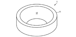
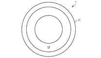
図1Aは、本発明のハウジングの例示的な実施形態の反射体を、概略的な斜視図として示している。図1Bは、この反射体を平面図として示している。反射体1は、環状に具体化されている。反射体1は、内側領域12を取り囲む表面11を有する。内側領域12は、電磁放射に対して反射性であるように具体化されている。
FIG. 1A shows the reflector of an exemplary embodiment of the housing of the present invention as a schematic perspective view. FIG. 1B shows this reflector as a plan view. The
反射体1は、本明細書に記載されている第1のプラスチック材料から形成されており、反射体1の放射反射特性を向上する目的で、このプラスチック材料には白色顔料が導入されている。
The
反射体1は、例えば、機械加工によって、または射出成形法によって、ハウジングの残りの要素とは個別に作製される。反射体1は、機械的に自立性であり堅い、ハウジングの要素であり、本明細書に記載されている製造方法によって、ハウジングの残りの要素に機械的にしっかりと結合されている。
The
図2Aは、本発明のハウジング100を備えた、本発明のオプトエレクトロニクス半導体デバイスの第1の例示的な実施形態を、概略的な断面図として示しており、図2Bは、対応する平面図を示している。
FIG. 2A shows a first exemplary embodiment of an optoelectronic semiconductor device of the present invention with a
ハウジング100は、図1Aおよび図1Bを参照しながら説明した反射体1を備えている。反射体1は、その表面11において、部分的にハウジング材2に直接接触している。
The
ハウジング材2は、射出成形法によって反射体1の上に射出成形されており、したがって、部分的に反射体1に直接接触している。すなわち、ハウジング材2は、結合手段を使用せずに反射体1に結合されている。この実施形態の場合、反射体1の内側領域12の全体にわたり、ハウジング材2が存在しない、または実質的に存在しない。ハウジング材2が実質的に存在しないとは、例えば、反射体1の内側領域12のうち面積比率で最大で10%、特に、最大で5%が、ハウジング材2によって覆われていることを意味する。
The
反射体1の材料は、例えば、その融点がハウジング材2の融点よりも低いように選択する。一例として、反射体1の融点は、ハウジング材2の融点よりも、少なくとも5℃、最大で30℃低い。これによって、射出成形による封止工程時に、反射体1が瞬間的に柔らかくなってハウジング材2に良好に接着するようにすることができる。
The material of the
しかしながら、反射体1の融点が、ハウジング材2の融点よりも高い、または等しいことも可能である。この場合、特に、ハウジング材2に面している反射体1の外側領域が粗面または多孔面として具体化され、したがって、溶融状態のハウジング材2を、反射体1の粗面または微細孔に入り込ませることができる。
However, the melting point of the
反射体1は、ハウジング100における開口部を形成しており、オプトエレクトロニクス半導体部品3(例えば放射放出半導体チップ)がこの開口部の中に配置されている。反射体1の内側領域12は、部品3を枠状に囲んでいる。
The
ハウジング100は、さらに、第1の接続領域6aおよび第2の接続領域6bを備えている。半導体部品3は、結合手段(例えば導電性接着剤またははんだ材料)によって第1の接続領域6aに結合されている。半導体部品3は、コンタクトワイヤ5によって第2の接続領域6bに導電接続されている。第1の接続領域6aおよび第2の接続領域6bは、反射体1と同じ射出成形工程における射出成形により、ハウジング材2によって包囲され、これによってハウジング材2に機械的に結合されることが好ましい。
The
ハウジング材2は第2のプラスチック材料によって形成されており、第2のプラスチック材料は、例えば、以下の材料、すなわち、ポリアミド、ポリフェニレンサルファイド、ポリエーテルイミド、ポリフェニルスルホン、のうちの少なくとも1種類を含んでいる。
The
光学特性および機械的安定性を設定するための充填材(例えばカーボンブラック、顔料、ガラス繊維の少なくとも1種類)を、第2のプラスチック材料の中に導入することができる。 A filler (eg, at least one of carbon black, pigment, glass fiber) for setting optical properties and mechanical stability can be introduced into the second plastic material.
図2Aおよび図2Bの例示的な実施形態においては、反射体1の表面11のうち、接続領域6a,6bとは反対側の上面には、ハウジング材2が存在しない。
In the exemplary embodiment of FIGS. 2A and 2B, the
これとは異なり、図3の例示的な実施形態においては、反射体1の上面がハウジング材2によって覆われており、ハウジング材に直接接触している。すなわち、この例示的な実施形態においては、ハウジング材2が存在しないのは、反射体1の内側領域12のみである。この例示的な実施形態においては、反射体1は、ハウジング材2に、特に良好な接着状態で機械的に結合されている。ハウジング材2に直接接触している反射体1の外側領域は、一例として、粗面化されている、もしくは多孔性である、またはその両方であり、反射体1の粗面もしくは微細孔またはその両方には、少なくとも部分的にハウジング材2が入り込んでいる。
In contrast, in the exemplary embodiment of FIG. 3, the top surface of the
ここまで、本発明について例示的な実施形態に基づいて説明してきたが、本発明はこれらの実施形態に限定されない。本発明は、任意の新規の特徴および特徴の任意の組合せを包含しており、特に、請求項における特徴の任意の組合せを含んでいる。これらの特徴または特徴の組合せは、それ自体が請求項あるいは例示的な実施形態に明示的に記載されていない場合であっても、本発明に含まれる。 So far, the present invention has been described based on exemplary embodiments, but the present invention is not limited to these embodiments. The invention encompasses any novel feature and any combination of features, particularly any combination of features in the claims. These features or combinations of features are included in the present invention even if they are not expressly recited in the claims or in the exemplary embodiments.
関連出願
本特許出願は、独国特許出願第102009058421.8号の優先権を主張し、この文書の開示内容は参照によって本出願に組み込まれている。
RELATED APPLICATION This patent application claims the priority of German patent application No. 10202588421.8, the disclosure content of which is incorporated into this application by reference.
Claims (15)
a) 電磁放射を反射するのに適している少なくとも1つの内側領域(12)を有する反射体(1)、を設けるステップと、
b) 前記反射体(1)を部分的にハウジング材(2)によって包囲する包囲ステップと、
を含んでおり、
− 前記包囲ステップが、射出成形法によって実施され、
− 前記反射体(1)の前記内側領域(12)には、少なくとも部分的に前記ハウジング材(2)が存在しておらず、
− 前記反射体(1)が第1のプラスチック材料によって形成され、
− 前記ハウジング材(2)が第2のプラスチック材料によって形成され、
− 前記第1のプラスチック材料が前記第2のプラスチック材料とは異なり、
− 熱的安定性および電磁放射に対する耐性、の少なくとも一方の材料特性に関して、前記第1のプラスチック材料と前記第2のプラスチック材料とが互いに異なる、
方法。 A method for manufacturing an optoelectronic semiconductor device housing (100) comprising:
a) providing a reflector (1) having at least one inner region (12) suitable for reflecting electromagnetic radiation;
b) an enclosing step of partially enclosing the reflector (1) by a housing material (2);
Contains
-The surrounding step is carried out by an injection molding method;
The housing material (2) is not present at least partially in the inner region (12) of the reflector (1);
The reflector (1) is formed of a first plastic material;
The housing material (2) is formed by a second plastic material;
The first plastic material is different from the second plastic material;
The first plastic material and the second plastic material are different from each other with respect to at least one material property of thermal stability and resistance to electromagnetic radiation;
Method.
請求項1に記載の方法。 -Before the step of providing the reflector (1), the reflector (1) is made by machining;
The method of claim 1.
請求項1に記載の方法。 -Before the step of providing the reflector (1), the reflector (1) is made by injection molding;
The method of claim 1.
請求項1から請求項3のいずれかに記載の方法。 When the reflector (1) is surrounded by the housing material (2) except at least a part of the inner region (12), the entire surface (11) of the reflector (1) is the housing material (2); Covered by the
4. A method according to any one of claims 1 to 3.
− 電磁放射を反射するのに適している少なくとも1つの内側領域(12)を有する反射体(1)と、
− 前記反射体(1)の前記表面(11)に少なくとも部分的に直接接触しているハウジング材(2)と、
を備えており、
− 前記反射体(1)と前記ハウジング材(2)が、結合手段を使用せずに互いに機械的に結合されており、
− 前記反射体(1)の前記内側領域(12)には、少なくとも一部分または全体にわたり、ハウジング材(2)が存在しておらず、
− 前記反射体(1)が第1のプラスチック材料によって形成されており、
− 前記ハウジング材(2)が第2のプラスチック材料によって形成されており、
− 前記第1のプラスチック材料が前記第2のプラスチック材料とは異なり、
− 熱的安定性および電磁放射に対する耐性、の少なくとも一方の材料特性に関して、前記第1のプラスチック材料と前記第2のプラスチック材料とが互いに異なる、
ハウジング。 Optoelectronic semiconductor device housing,
A reflector (1) having at least one inner region (12) suitable for reflecting electromagnetic radiation;
A housing material (2) that is at least partly in direct contact with the surface (11) of the reflector (1);
With
The reflector (1) and the housing material (2) are mechanically coupled to each other without the use of coupling means;
The housing region (2) is not present at least partially or entirely in the inner region (12) of the reflector (1);
The reflector (1) is made of a first plastic material;
The housing material (2) is formed of a second plastic material;
The first plastic material is different from the second plastic material;
The first plastic material and the second plastic material are different from each other with respect to at least one material property of thermal stability and resistance to electromagnetic radiation;
housing.
請求項5に記載のハウジング。 The reflector (1) and the housing material (2) are mechanically coupled to each other by injection molding;
The housing according to claim 5.
請求項5または請求項6に記載のハウジング。 The housing material (2) and the reflector (1) are different from each other in terms of optical properties;
The housing according to claim 5 or 6.
請求項5から請求項7のいずれかに記載のハウジング。 The reflector (1) has a reflectivity of at least 80% for at least one of ultraviolet radiation, visible radiation, infrared radiation;
The housing according to any one of claims 5 to 7.
請求項5から請求項8のいずれかに記載のハウジング。 The reflector (1) comprises a second plastic material and a white pigment;
The housing according to any one of claims 5 to 8.
請求項9に記載のハウジング。 The white pigment comprises at least one of the following materials: titanium dioxide, lithopone, barium sulfate, zinc oxide, zinc sulfide, zirconium dioxide, chalk;
The housing according to claim 9.
請求項5から請求項10のいずれかに記載のハウジング。 The first plastic material is a group consisting of at least one of the following materials: polyester, fluoropolymer, polyetherketone, polyetherimide, high temperature polyamide, polyetherketone, liquid crystal polymer, silicone; Selected from the
The housing according to any one of claims 5 to 10.
請求項5から請求項11のいずれかに記載のハウジング。 The second plastic material is selected from the group consisting of at least one of the following materials: polyamide, polyphenylene sulfide, polyetherimide, polyphenylsulfone,
The housing according to any one of claims 5 to 11.
請求項5から請求項12のいずれかに記載のハウジング。 The first plastic material has a lower melting point than the second plastic material;
The housing according to any one of claims 5 to 12.
請求項5から請求項13のいずれかに記載のハウジング。 The outer region of the reflector (1) that is in direct contact with the housing material (2) is roughened or perforated, or both, of the reflector (1) The housing material (2) enters at least partially in the rough surface or the fine hole,
The housing according to any one of claims 5 to 13.
− 請求項5から請求項14のいずれかに記載のハウジング(100)と、
− 少なくとも1個のオプトエレクトロニクス部品(3)、特に、放射放出半導体チップと、
を備えており、
− 前記少なくとも1個のオプトエレクトロニクス部品(3)が、前記反射体の前記少なくとも1つの内側領域によって横方向に囲まれている、
オプトエレクトロニクスデバイス。
An optoelectronic device,
A housing (100) according to any of claims 5 to 14,
At least one optoelectronic component (3), in particular a radiation-emitting semiconductor chip;
With
The at least one optoelectronic component (3) is laterally surrounded by the at least one inner region of the reflector;
Optoelectronic devices.
Applications Claiming Priority (3)
| Application Number | Priority Date | Filing Date | Title |
|---|---|---|---|
| DE102009058421.8 | 2009-12-16 | ||
| DE102009058421A DE102009058421A1 (en) | 2009-12-16 | 2009-12-16 | Method for producing a housing for an optoelectronic semiconductor component, housing and optoelectronic semiconductor component |
| PCT/EP2010/067705 WO2011082876A1 (en) | 2009-12-16 | 2010-11-17 | Method for producing a housing for an optoelectronic semiconductor component, housing, and optoelectronic semiconductor component |
Publications (2)
| Publication Number | Publication Date |
|---|---|
| JP2013514641A true JP2013514641A (en) | 2013-04-25 |
| JP2013514641A5 JP2013514641A5 (en) | 2013-12-12 |
Family
ID=43608617
Family Applications (1)
| Application Number | Title | Priority Date | Filing Date |
|---|---|---|---|
| JP2012543566A Withdrawn JP2013514641A (en) | 2009-12-16 | 2010-11-17 | Optoelectronic semiconductor component housing manufacturing method, housing, and optoelectronic semiconductor component |
Country Status (7)
| Country | Link |
|---|---|
| US (1) | US9331255B2 (en) |
| EP (1) | EP2513985A1 (en) |
| JP (1) | JP2013514641A (en) |
| KR (1) | KR20120106808A (en) |
| CN (1) | CN102668144A (en) |
| DE (1) | DE102009058421A1 (en) |
| WO (1) | WO2011082876A1 (en) |
Cited By (6)
| Publication number | Priority date | Publication date | Assignee | Title |
|---|---|---|---|---|
| JP2016019001A (en) * | 2014-07-08 | 2016-02-01 | エルジー イノテック カンパニー リミテッド | Light emitting element package |
| JP2016019000A (en) * | 2014-07-08 | 2016-02-01 | エルジー イノテック カンパニー リミテッド | Light emitting element package |
| KR20170094859A (en) * | 2016-02-12 | 2017-08-22 | 엘지이노텍 주식회사 | Light emitting device package and lighting apparatus including the package |
| JPWO2016194120A1 (en) * | 2015-06-01 | 2017-08-24 | 三菱電機株式会社 | Light emitting device, display unit, and video display device |
| KR20170099557A (en) * | 2016-02-24 | 2017-09-01 | 엘지이노텍 주식회사 | Light emitting device package and lighting apparatus including the package |
| CN108633317A (en) * | 2016-02-12 | 2018-10-09 | Lg 伊诺特有限公司 | Light emitting device package and lighting apparatus including the light emitting device package |
Families Citing this family (9)
| Publication number | Priority date | Publication date | Assignee | Title |
|---|---|---|---|---|
| WO2013073897A2 (en) | 2011-11-17 | 2013-05-23 | 주식회사 루멘스 | Light emitting device package and backlight including same |
| KR101640331B1 (en) * | 2011-11-24 | 2016-07-15 | 크리 후이저우 솔리드 스테이트 라이팅 컴패니 리미티드 | Water resistant led devices and led display including the same |
| TW201432949A (en) * | 2013-02-05 | 2014-08-16 | Lextar Electronics Corp | Lighting module and manufacturing method thereof |
| KR20140141227A (en) * | 2013-05-31 | 2014-12-10 | 제일모직주식회사 | Polyamide-Based Resin Composition Having Excellent Reflectance and Discoloration Resistance |
| WO2015157178A1 (en) * | 2014-04-07 | 2015-10-15 | Crystal Is, Inc. | Ultraviolet light-emitting devices and methods |
| DE102014105839A1 (en) * | 2014-04-25 | 2015-10-29 | Osram Opto Semiconductors Gmbh | Optoelectronic component and method for producing an optoelectronic component |
| DE102016103059A1 (en) * | 2016-02-22 | 2017-08-24 | Osram Opto Semiconductors Gmbh | Semiconductor device and method for manufacturing a semiconductor device |
| DE102016105243A1 (en) * | 2016-03-21 | 2017-09-21 | Infineon Technologies Ag | Spatially Selective roughening of encapsulant to promote adhesion with a functional structure |
| CN112816071B (en) * | 2021-01-06 | 2021-12-28 | 国家卫星气象中心(国家空间天气监测预警中心) | Infrared channel radiation stability monitoring method based on cloud top height algorithm |
Family Cites Families (30)
| Publication number | Priority date | Publication date | Assignee | Title |
|---|---|---|---|---|
| DE19829197C2 (en) | 1998-06-30 | 2002-06-20 | Siemens Ag | Component emitting and / or receiving radiation |
| DE19945133C2 (en) | 1999-09-21 | 2002-06-27 | Osram Opto Semiconductors Gmbh | Surface mount housing for detector components with side light sensitivity |
| CN1259732C (en) * | 2000-09-29 | 2006-06-14 | 欧姆龙株式会社 | Optical device for optical element and equipment using the same |
| JP2002374007A (en) * | 2001-06-15 | 2002-12-26 | Toyoda Gosei Co Ltd | Light-emitting apparatus |
| JP4211359B2 (en) * | 2002-03-06 | 2009-01-21 | 日亜化学工業株式会社 | Manufacturing method of semiconductor device |
| JP3912607B2 (en) * | 2002-06-19 | 2007-05-09 | サンケン電気株式会社 | Manufacturing method of semiconductor light emitting device |
| TWI292961B (en) * | 2002-09-05 | 2008-01-21 | Nichia Corp | Semiconductor device and an optical device using the semiconductor device |
| KR101025234B1 (en) * | 2003-02-28 | 2011-04-01 | 오스람 옵토 세미컨덕터스 게엠베하 | Optoelectronic component comprising a housing body which is metallised in a structured manner, method for producing one such component, and method for the structured metallisation of a body containing plastic |
| JP4182783B2 (en) * | 2003-03-14 | 2008-11-19 | 豊田合成株式会社 | LED package |
| DE10323857A1 (en) * | 2003-05-26 | 2005-01-27 | Osram Opto Semiconductors Gmbh | Housing for a laser diode device, laser diode device and method of manufacturing a laser diode device |
| DE10360943A1 (en) * | 2003-12-23 | 2005-07-21 | Engel, Hartmut S. | lighting device |
| JP2005243973A (en) * | 2004-02-26 | 2005-09-08 | Kyocera Corp | Light-emitting device and luminaire |
| DE102004053116A1 (en) * | 2004-11-03 | 2006-05-04 | Tridonic Optoelectronics Gmbh | Light-emitting diode arrangement with color conversion material |
| JP2006186297A (en) * | 2004-12-03 | 2006-07-13 | Toshiba Corp | Semiconductor light emitting device and its manufacturing method |
| KR100580753B1 (en) * | 2004-12-17 | 2006-05-15 | 엘지이노텍 주식회사 | Light emitting device package |
| JP5065888B2 (en) * | 2005-03-24 | 2012-11-07 | 京セラ株式会社 | Light emitting device and lighting device |
| KR100631992B1 (en) * | 2005-07-19 | 2006-10-09 | 삼성전기주식회사 | Light emitting diode package having dual lens structure for laterally emitting light |
| CN101846247B (en) * | 2005-12-22 | 2013-04-17 | 松下电器产业株式会社 | Lighting apparatus with LED |
| JP2007305785A (en) * | 2006-05-11 | 2007-11-22 | Nichia Chem Ind Ltd | Light emitting device |
| WO2007146295A2 (en) * | 2006-06-13 | 2007-12-21 | Powerweb Technologies, Inc. | Led light pod with modular optics and heat dissipation structure |
| US8367945B2 (en) | 2006-08-16 | 2013-02-05 | Cree Huizhou Opto Limited | Apparatus, system and method for use in mounting electronic elements |
| JP4846498B2 (en) * | 2006-09-22 | 2011-12-28 | 株式会社東芝 | Optical semiconductor device and method for manufacturing optical semiconductor device |
| DE102006046678A1 (en) * | 2006-09-29 | 2008-04-03 | Osram Opto Semiconductors Gmbh | Housing for use with semiconductor body of e.g. LED unit, has plastic-base body with plastic components, where one plastic component is made of material differing from that of other component in optical characteristic |
| KR100801621B1 (en) * | 2007-06-05 | 2008-02-11 | 서울반도체 주식회사 | Led package |
| JP2008305940A (en) * | 2007-06-07 | 2008-12-18 | Showa Denko Kk | Display, cap, light-emitting device, and manufacturing methods of same display, cap, and light-emitting device |
| WO2009114783A1 (en) * | 2008-03-13 | 2009-09-17 | Fraen Corporation | Reflective variable spot size lighting devices and systems |
| US20100032702A1 (en) * | 2008-08-11 | 2010-02-11 | E. I. Du Pont De Nemours And Company | Light-Emitting Diode Housing Comprising Fluoropolymer |
| DE102008038748B4 (en) | 2008-08-12 | 2022-08-04 | OSRAM Opto Semiconductors Gesellschaft mit beschränkter Haftung | Surface-mount optoelectronic semiconductor component |
| DE102009033287A1 (en) * | 2009-07-15 | 2011-01-20 | Osram Opto Semiconductors Gmbh | Light-emitting diode and method for producing a light-emitting diode |
| US8585253B2 (en) * | 2009-08-20 | 2013-11-19 | Illumitex, Inc. | System and method for color mixing lens array |
-
2009
- 2009-12-16 DE DE102009058421A patent/DE102009058421A1/en not_active Withdrawn
-
2010
- 2010-11-17 US US13/513,784 patent/US9331255B2/en not_active Expired - Fee Related
- 2010-11-17 CN CN2010800577362A patent/CN102668144A/en active Pending
- 2010-11-17 EP EP10788034A patent/EP2513985A1/en not_active Withdrawn
- 2010-11-17 JP JP2012543566A patent/JP2013514641A/en not_active Withdrawn
- 2010-11-17 WO PCT/EP2010/067705 patent/WO2011082876A1/en active Application Filing
- 2010-11-17 KR KR1020127018624A patent/KR20120106808A/en not_active Application Discontinuation
Cited By (10)
| Publication number | Priority date | Publication date | Assignee | Title |
|---|---|---|---|---|
| JP2016019001A (en) * | 2014-07-08 | 2016-02-01 | エルジー イノテック カンパニー リミテッド | Light emitting element package |
| JP2016019000A (en) * | 2014-07-08 | 2016-02-01 | エルジー イノテック カンパニー リミテッド | Light emitting element package |
| JPWO2016194120A1 (en) * | 2015-06-01 | 2017-08-24 | 三菱電機株式会社 | Light emitting device, display unit, and video display device |
| US10256383B2 (en) | 2015-06-01 | 2019-04-09 | Mitsubishi Electric Corporation | Light emitting device with dark area and greater reflectance light area, display unit, and image display device |
| KR20170094859A (en) * | 2016-02-12 | 2017-08-22 | 엘지이노텍 주식회사 | Light emitting device package and lighting apparatus including the package |
| CN108633317A (en) * | 2016-02-12 | 2018-10-09 | Lg 伊诺特有限公司 | Light emitting device package and lighting apparatus including the light emitting device package |
| JP2019505097A (en) * | 2016-02-12 | 2019-02-21 | エルジー イノテック カンパニー リミテッド | Light emitting device package and lighting device including the same |
| KR102562091B1 (en) | 2016-02-12 | 2023-08-02 | 쑤저우 레킨 세미컨덕터 컴퍼니 리미티드 | Light emitting device package |
| KR20170099557A (en) * | 2016-02-24 | 2017-09-01 | 엘지이노텍 주식회사 | Light emitting device package and lighting apparatus including the package |
| KR102509312B1 (en) * | 2016-02-24 | 2023-03-17 | 쑤저우 레킨 세미컨덕터 컴퍼니 리미티드 | Light emitting device package |
Also Published As
| Publication number | Publication date |
|---|---|
| DE102009058421A1 (en) | 2011-06-22 |
| WO2011082876A1 (en) | 2011-07-14 |
| US9331255B2 (en) | 2016-05-03 |
| KR20120106808A (en) | 2012-09-26 |
| CN102668144A (en) | 2012-09-12 |
| EP2513985A1 (en) | 2012-10-24 |
| US20120280116A1 (en) | 2012-11-08 |
Similar Documents
| Publication | Publication Date | Title |
|---|---|---|
| JP2013514641A (en) | Optoelectronic semiconductor component housing manufacturing method, housing, and optoelectronic semiconductor component | |
| KR101403168B1 (en) | Optical element for a light-emitting diode, light-emitting diode, led arrangement and method for producing an led arrangement | |
| RU2488195C2 (en) | Assembly of light-emitting diode (led) lead-frame unit, led group using this lead-frame and method for manufacturing of led group | |
| EP2215667B1 (en) | Method for fabricating an led package | |
| US20110062470A1 (en) | Reduced angular emission cone illumination leds | |
| TWI440227B (en) | Housing, optoelectronic component and method for producing a housing | |
| KR101454932B1 (en) | Optical element, production method therefor, and composite component provided with an optical element | |
| US9837392B2 (en) | LED lighting apparatus | |
| EP1801893A2 (en) | Lens-equipped light-emitting diode device and method of manufacturing the same | |
| JP5436677B2 (en) | Potted photoelectric module having a plurality of semiconductor elements, and method for manufacturing photoelectric module | |
| JP2007311445A (en) | Semiconductor light-emitting device, and manufacturing method thereof | |
| KR20090031446A (en) | Lighting device package | |
| KR20090075806A (en) | Housing for an optoelectronic component, optoelectronic component and method for producing a housing for an optoelectronic component | |
| KR20150092423A (en) | Light emitting device package | |
| KR101896682B1 (en) | Light emitting device and lighting apparatus having thereof | |
| JP7007591B2 (en) | Luminous module | |
| JP2015176946A (en) | Led light emitting device | |
| JP6928289B2 (en) | Luminous module | |
| KR101861232B1 (en) | Light emitting module | |
| JP2007311674A (en) | Semiconductor light-emitting device | |
| KR102432222B1 (en) | Optical plate, lighting device, and lighting module | |
| KR101334315B1 (en) | Light emitting diode lamp and method of fabricating the same | |
| JP2008235719A (en) | Illumination apparatus | |
| KR101334314B1 (en) | Light emitting diode lamp and method of fabricating the same | |
| US7977692B2 (en) | SMT LED with high light output for high power applications |
Legal Events
| Date | Code | Title | Description |
|---|---|---|---|
| A521 | Written amendment |
Free format text: JAPANESE INTERMEDIATE CODE: A523 Effective date: 20131023 |
|
| A621 | Written request for application examination |
Free format text: JAPANESE INTERMEDIATE CODE: A621 Effective date: 20131023 |
|
| A761 | Written withdrawal of application |
Free format text: JAPANESE INTERMEDIATE CODE: A761 Effective date: 20140310 |