EP2782102A1 - Elektrodenpastenzusammensetzung, solarzellenelement und solarzelle - Google Patents
Elektrodenpastenzusammensetzung, solarzellenelement und solarzelle Download PDFInfo
- Publication number
- EP2782102A1 EP2782102A1 EP12849394.7A EP12849394A EP2782102A1 EP 2782102 A1 EP2782102 A1 EP 2782102A1 EP 12849394 A EP12849394 A EP 12849394A EP 2782102 A1 EP2782102 A1 EP 2782102A1
- Authority
- EP
- European Patent Office
- Prior art keywords
- particle
- electrode
- mass
- paste composition
- tin
- Prior art date
- Legal status (The legal status is an assumption and is not a legal conclusion. Google has not performed a legal analysis and makes no representation as to the accuracy of the status listed.)
- Withdrawn
Links
Images


Classifications
-
- H—ELECTRICITY
- H01—ELECTRIC ELEMENTS
- H01B—CABLES; CONDUCTORS; INSULATORS; SELECTION OF MATERIALS FOR THEIR CONDUCTIVE, INSULATING OR DIELECTRIC PROPERTIES
- H01B1/00—Conductors or conductive bodies characterised by the conductive materials; Selection of materials as conductors
- H01B1/20—Conductive material dispersed in non-conductive organic material
- H01B1/22—Conductive material dispersed in non-conductive organic material the conductive material comprising metals or alloys
-
- H—ELECTRICITY
- H10—SEMICONDUCTOR DEVICES; ELECTRIC SOLID-STATE DEVICES NOT OTHERWISE PROVIDED FOR
- H10K—ORGANIC ELECTRIC SOLID-STATE DEVICES
- H10K10/00—Organic devices specially adapted for rectifying, amplifying, oscillating or switching; Organic capacitors or resistors having potential barriers
- H10K10/80—Constructional details
- H10K10/82—Electrodes
-
- C—CHEMISTRY; METALLURGY
- C03—GLASS; MINERAL OR SLAG WOOL
- C03C—CHEMICAL COMPOSITION OF GLASSES, GLAZES OR VITREOUS ENAMELS; SURFACE TREATMENT OF GLASS; SURFACE TREATMENT OF FIBRES OR FILAMENTS MADE FROM GLASS, MINERALS OR SLAGS; JOINING GLASS TO GLASS OR OTHER MATERIALS
- C03C8/00—Enamels; Glazes; Fusion seal compositions being frit compositions having non-frit additions
- C03C8/14—Glass frit mixtures having non-frit additions, e.g. opacifiers, colorants, mill-additions
- C03C8/18—Glass frit mixtures having non-frit additions, e.g. opacifiers, colorants, mill-additions containing free metals
-
- C—CHEMISTRY; METALLURGY
- C22—METALLURGY; FERROUS OR NON-FERROUS ALLOYS; TREATMENT OF ALLOYS OR NON-FERROUS METALS
- C22C—ALLOYS
- C22C12/00—Alloys based on antimony or bismuth
-
- C—CHEMISTRY; METALLURGY
- C22—METALLURGY; FERROUS OR NON-FERROUS ALLOYS; TREATMENT OF ALLOYS OR NON-FERROUS METALS
- C22C—ALLOYS
- C22C13/00—Alloys based on tin
-
- C—CHEMISTRY; METALLURGY
- C22—METALLURGY; FERROUS OR NON-FERROUS ALLOYS; TREATMENT OF ALLOYS OR NON-FERROUS METALS
- C22C—ALLOYS
- C22C13/00—Alloys based on tin
- C22C13/02—Alloys based on tin with antimony or bismuth as the next major constituent
-
- C—CHEMISTRY; METALLURGY
- C22—METALLURGY; FERROUS OR NON-FERROUS ALLOYS; TREATMENT OF ALLOYS OR NON-FERROUS METALS
- C22C—ALLOYS
- C22C19/00—Alloys based on nickel or cobalt
-
- C—CHEMISTRY; METALLURGY
- C22—METALLURGY; FERROUS OR NON-FERROUS ALLOYS; TREATMENT OF ALLOYS OR NON-FERROUS METALS
- C22C—ALLOYS
- C22C19/00—Alloys based on nickel or cobalt
- C22C19/03—Alloys based on nickel or cobalt based on nickel
-
- C—CHEMISTRY; METALLURGY
- C22—METALLURGY; FERROUS OR NON-FERROUS ALLOYS; TREATMENT OF ALLOYS OR NON-FERROUS METALS
- C22C—ALLOYS
- C22C19/00—Alloys based on nickel or cobalt
- C22C19/03—Alloys based on nickel or cobalt based on nickel
- C22C19/05—Alloys based on nickel or cobalt based on nickel with chromium
- C22C19/058—Alloys based on nickel or cobalt based on nickel with chromium without Mo and W
-
- C—CHEMISTRY; METALLURGY
- C22—METALLURGY; FERROUS OR NON-FERROUS ALLOYS; TREATMENT OF ALLOYS OR NON-FERROUS METALS
- C22C—ALLOYS
- C22C38/00—Ferrous alloys, e.g. steel alloys
- C22C38/08—Ferrous alloys, e.g. steel alloys containing nickel
-
- C—CHEMISTRY; METALLURGY
- C22—METALLURGY; FERROUS OR NON-FERROUS ALLOYS; TREATMENT OF ALLOYS OR NON-FERROUS METALS
- C22C—ALLOYS
- C22C9/00—Alloys based on copper
-
- C—CHEMISTRY; METALLURGY
- C22—METALLURGY; FERROUS OR NON-FERROUS ALLOYS; TREATMENT OF ALLOYS OR NON-FERROUS METALS
- C22C—ALLOYS
- C22C9/00—Alloys based on copper
- C22C9/06—Alloys based on copper with nickel or cobalt as the next major constituent
-
- H—ELECTRICITY
- H10—SEMICONDUCTOR DEVICES; ELECTRIC SOLID-STATE DEVICES NOT OTHERWISE PROVIDED FOR
- H10F—INORGANIC SEMICONDUCTOR DEVICES SENSITIVE TO INFRARED RADIATION, LIGHT, ELECTROMAGNETIC RADIATION OF SHORTER WAVELENGTH OR CORPUSCULAR RADIATION
- H10F10/00—Individual photovoltaic cells, e.g. solar cells
- H10F10/10—Individual photovoltaic cells, e.g. solar cells having potential barriers
- H10F10/14—Photovoltaic cells having only PN homojunction potential barriers
- H10F10/146—Back-junction photovoltaic cells, e.g. having interdigitated base-emitter regions on the back side
-
- H—ELECTRICITY
- H10—SEMICONDUCTOR DEVICES; ELECTRIC SOLID-STATE DEVICES NOT OTHERWISE PROVIDED FOR
- H10F—INORGANIC SEMICONDUCTOR DEVICES SENSITIVE TO INFRARED RADIATION, LIGHT, ELECTROMAGNETIC RADIATION OF SHORTER WAVELENGTH OR CORPUSCULAR RADIATION
- H10F77/00—Constructional details of devices covered by this subclass
- H10F77/20—Electrodes
- H10F77/206—Electrodes for devices having potential barriers
- H10F77/211—Electrodes for devices having potential barriers for photovoltaic cells
- H10F77/219—Arrangements for electrodes of back-contact photovoltaic cells
- H10F77/223—Arrangements for electrodes of back-contact photovoltaic cells for metallisation wrap-through [MWT] photovoltaic cells
-
- H—ELECTRICITY
- H10—SEMICONDUCTOR DEVICES; ELECTRIC SOLID-STATE DEVICES NOT OTHERWISE PROVIDED FOR
- H10F—INORGANIC SEMICONDUCTOR DEVICES SENSITIVE TO INFRARED RADIATION, LIGHT, ELECTROMAGNETIC RADIATION OF SHORTER WAVELENGTH OR CORPUSCULAR RADIATION
- H10F77/00—Constructional details of devices covered by this subclass
- H10F77/20—Electrodes
- H10F77/206—Electrodes for devices having potential barriers
- H10F77/211—Electrodes for devices having potential barriers for photovoltaic cells
- H10F77/219—Arrangements for electrodes of back-contact photovoltaic cells
- H10F77/227—Arrangements for electrodes of back-contact photovoltaic cells for emitter wrap-through [EWT] photovoltaic cells, e.g. interdigitated emitter-base back-contacts
-
- Y—GENERAL TAGGING OF NEW TECHNOLOGICAL DEVELOPMENTS; GENERAL TAGGING OF CROSS-SECTIONAL TECHNOLOGIES SPANNING OVER SEVERAL SECTIONS OF THE IPC; TECHNICAL SUBJECTS COVERED BY FORMER USPC CROSS-REFERENCE ART COLLECTIONS [XRACs] AND DIGESTS
- Y02—TECHNOLOGIES OR APPLICATIONS FOR MITIGATION OR ADAPTATION AGAINST CLIMATE CHANGE
- Y02E—REDUCTION OF GREENHOUSE GAS [GHG] EMISSIONS, RELATED TO ENERGY GENERATION, TRANSMISSION OR DISTRIBUTION
- Y02E10/00—Energy generation through renewable energy sources
- Y02E10/50—Photovoltaic [PV] energy
- Y02E10/547—Monocrystalline silicon PV cells
Definitions
- the present invention relates to a paste composition for an electrode, a photovoltaic cell element, and a photovoltaic cell.
- electrodes are formed on a light receiving surface and a back surface of a silicon based photovoltaic cell.
- the electrodes In order to output efficiently the electrical energy converted in a photovoltaic cell from incident light, it is necessary that the electrodes have sufficiently low volume resistivity and form a favorable ohmic contact with the silicon substrate.
- an electrode on the light receiving surface to have a thin electrode width and a high electrode aspect ratio, in order to limit the incidence loss of sunlight to the minimum.
- An electrode used on a light receiving surface of a photovoltaic cell is usually formed as follows. Namely, a texture (asperity) is formed on the light receiving surface side of a p-type silicon substrate; then by diffusing thermally phosphorus or the like at a high temperature to form an n-type silicon layer, on which a conductive composition is provided by screen printing or the like, followed by sintering in the atmosphere at 800°C to 900°C to form a light receiving surface electrode.
- the conductive composition for forming a light receiving surface electrode contains a conductive metal powder, a glass particle, various additives, and the like.
- the conductive metal powder usually a silver powder is used.
- the reasons thereof include: the volume resistivity of a silver particle is as low as 1.6 ⁇ 10 -6 ⁇ cm; a silver particle can be sintered under the sintering condition mentioned above through auto-reduction; a favorable ohmic contact with a silicon substrate can be established; and the wettability of a solder material to an electrode made of a silver particle is superior, so that wiring materials such as a tab wire connecting electrically photovoltaic cell elements each other in forming a module system encapsulating photovoltaic cell elements with a glass substrate or the like can be well bonded.
- a conductive composition containing a silver particle exhibits favorable characteristics as an electrode for a photovoltaic cell.
- silver is a noble metal and the base metal itself is expensive, and in perspective of a resource issue, a proposal of a conductive composition replacing a silver-containing conductive composition has been desired.
- Examples of a promising material replacing silver include a copper, which is utilized as a semiconductor wiring material. Copper is abundant in terms of resources and the cost of the base metal is approx. hundredth as low as silver. However, copper is a material that easily oxidizes at a high temperature of 200°C or higher in the atmosphere and consequently it is difficult to form an electrode according to the above described process.
- a copper particle which is hard to be oxidized by a high temperature sintering through imparting oxidation resistance to copper by means of various techniques (For example, see Japanese Patent Laid-Open (JP-A) No. 2005-314755 and JP-A No. 2004-217952 ).
- the oxidation resistance of the copper particles is limited to 300°C at most and at a temperature as high as 800°C to 900°C substantially all of them are oxidized, and consequently they have been not yet commercialized as a photovoltaic cell electrode. Further, since additives and the like added for imparting oxidation resistance disturb sintering of copper particles during sintering, there is consequently a problem that an electrode with such low volume resistivity as silver cannot be obtained.
- the formed Cu 3 Si may occasionally reach the depth of several ⁇ m from the interface and sometimes cause a crack on the silicon substrate side. Further, in some cases it may penetrate through an n-type silicon layer formed previously on the silicon substrate and deteriorate the semiconductor performance (pn-junction property) of the photovoltaic cell. Further, the formed Cu 3 Si may lift up an electrode made of copper, which may result in the inhibition of the adhesion with the silicon substrate and a decrease in the mechanical strength of the electrode.
- the present invention was made in view of the problems with an object to provide a paste composition for an electrode, which can form an electrode with low resistivity, and further form a copper-containing electrode having a favorable ohmic contact with the silicon substrate, as well as a photovoltaic cell element and a photovoltaic cell having an electrode formed with the paste composition for an electrode.
- the inventors of the present invention studied intensively to complete the present invention. More particularly, the present invention is as follows.
- a paste composition for an electrode which is capable of forming an electrode with low resistivity, and further forming a copper-containing electrode having a favorable ohmic contact with the silicon substrate, as well as a photovoltaic cell element and a photovoltaic cell having an electrode formed with the paste composition for an electrode can be provided.
- step encompasses not only an independent step but also a step in which the anticipated effect of this step is achieved, even if the step cannot be clearly distinguished from another step.
- a numerical value range indicated by use of the term “to” as used herein refers to a range including the numerical values described before and after “to” as the minimum and maximum values, respectively. Unless specifically indicated, in a case in which each ingredient of a composition includes plural materials, the content of each ingredient of the composition denotes the total amount of the plural materials included in the composition.
- a paste composition for an electrode according to the present invention contains at least one phosphorus-containing copper alloy particle, at least one tin-containing particle, at least one nickel-containing particle, at least one glass particle, at least one solvent, and at least one resin.
- a Cu-Sn alloy phase and a Sn-P-O glass phase are formed by a reaction between the phosphorus-containing copper alloy particle and tin-containing particle.
- an electrode with low volume resistivity can be formed.
- the paste composition for an electrode further contains nickel-containing particle. As the result, it is considered that the Cu-Sn alloy phase and the nickel-containing particle further react with each other to form a Cu-Sn-Ni alloy phase.
- the Cu-Sn-Ni alloy phase is also formed at a relatively high temperature as high as 800°C, it is considered that an electrode with volume resistivity can be formed, while maintaining the oxidation resistance even in a sintering process at a higher temperature.
- use of the paste composition for an electrode can respond to a variety of conditions such as sintering an electrode at a low temperature to a high temperature. Accordingly, the paste composition for an electrode can be widely used as an electrode material for photovoltaic cells with the below-mentioned various structures.
- the above Cu-Sn-Ni alloy phase forms a compact bulk in the electrode between Cu-Sn-Ni alloy phases or together with a Cu-Sn alloy phase which is further formed corresponding to a sintering condition, which functions as a conductive layer to form an electrode with low resistivity. It is thought that coexistence of the Cu-Sn alloy phase and the Cu-Sn-Ni alloy phase in the electrode does not decrease functions (for example, low volume resistivity).
- a compact bulk herein means a three-dimensional continuous structure constituted by massive Cu-Sn alloy phases and Cu-Sn-Ni alloy phases contacting each other compactly.
- an electrode is formed using a paste composition for an electrode on a substrate containing silicon (hereinafter also referred to simply as "silicon substrate")
- a paste composition for an electrode on a substrate containing silicon hereinafter also referred to simply as "silicon substrate”
- silicon substrate a substrate containing silicon
- a phosphorus-containing copper alloy particle, a tin-containing particle and a nickel-containing particle react with each other in a sintering process to form an electrode composed of a Cu-Sn-Ni alloy phase, a Sn-P-O glass phase and Cu-Sn alloy phase formed corresponding to a sintering condition.
- the Sn-P-O glass phase is formed between the Cu-Sn-Ni alloy phase and the silicon substrate or between the Cu-Sn-Ni alloy phase and the Cu-Sn alloy phase and the silicon substrate, which is believed to improve the adhesion of the Cu-Sn alloy phase and the Cu-Sn-Ni alloy phase to the silicon substrate. Further, it is so conceivable that a favorable ohmic contact between an electrode formed by sintering and a silicon substrate can be established by the Sn-P-O glass phase functioning as a barrier layer prohibiting interdiffusion of copper and silicon.
- a phosphorus-containing copper alloy particle by combining a phosphorus-containing copper alloy particle with a tin-containing particle and a nickel-containing particle in the paste composition for an electrode, and firstly utilizing the reducing property of a phosphorus atom in a phosphorus-containing copper alloy particle with respect to an oxidized copper, an electrode having superior oxidation resistance and low volume resistivity is formed.
- a reaction between the phosphorus-containing copper alloy particle and the tin-containing particle and the nickel-containing particle while maintaining the volume resistivity low, a conductive layer composed of a Cu-Sn-Ni alloy phase and a Cu-Sn alloy phase formed corresponding to a sintering condition, and an Sn-P-O glass phase are formed.
- the Sn-P-O glass phase functioning as a barrier layer that prevents the interdiffusion of copper and silicon, the formation of a reactant phase between the electrode and the silicon substrate is suppressed, and a favorable ohmic contact with the copper electrode can be established. It is conceivable that the above two characteristic mechanisms can be exercised in a series of sintering processes.
- Such an effect can be generally exerted when an electrode is formed with a paste composition for an electrode according to the present invention on a substrate containing silicon, and there is no particular restriction on a type of a substrate containing silicon.
- a substrate containing silicon include a silicon substrate for constituting a photovoltaic cell and a silicon substrate for producing a semiconductor device other than a photovoltaic cell.
- the paste composition for an electrode contains at least one phosphorus-containing copper alloy particle.
- a brazing material called copper phosphorus brazing (phosphorous concentration: approximately 7% by mass or less) is known.
- the copper phosphorus brazing is used as a copper-to-copper bonding agent, but by using the phosphorous-containing copper alloy particles in the paste composition for an electrode according to the present invention, and utilizing the reduction property of phosphorous with respect to a copper oxide, an electrode having an excellent oxidation resistance and a low volume resistivity can be formed. Furthermore, it becomes possible to sinter the electrode at a low temperature, and as a result, an effect of reducing a process cost can be attained.
- the content of phosphorous included in the phosphorous-containing copper alloy particle is preferably from 6% by mass to 8% by mass, more preferably from 6.3% by mass to 7.8% by mass, and even more preferably from 6.5% by mass to 7.5% by mass.
- the content of phosphorous included in the phosphorous-containing copper alloy is preferably from 6% by mass to 8% by mass, more preferably from 6.3% by mass to 7.8% by mass, and even more preferably from 6.5% by mass to 7.5% by mass.
- the content of phosphorous included in the phosphorous-containing copper alloy can be measured by using a high frequency inductively-coupled plasma atomic emission spectrometer (ICP-AES).
- ICP-AES inductively-coupled plasma atomic emission spectrometer
- the phosphorous-containing copper alloy particle is an alloy including copper and phosphorous and it may further contain other atoms.
- other atoms include Ag, Mn, Sb, Si, K, Na, Li, Ba, Sr, Ca, Mg, Be, Zn, Pb, Cd, Tl, V, Sn, Al, Zr, W, Mo, Ti, Co, Ni, and Au.
- the content of other atoms included in the phosphorous-containing copper alloy particle can be set to, for example, 3% by mass or less in the phosphorous-containing copper alloy particle, and from the perspectives of the oxidation resistance and low volume resistivity, it is preferably 1% by mass or less.
- the phosphorous-containing copper alloy particle may be used singly or in combination of two or more kinds thereof.
- the average particle diameter of the phosphorous-containing copper alloy particle is not particularly limited, and it is preferably from 0.4 ⁇ m to 10 ⁇ m, and more preferably from 1 ⁇ m to 7 ⁇ m in terms of an average particle diameter when the cumulative weight is 50% (hereinafter abbreviated as "D50%" in some cases).
- D50% average particle diameter when the cumulative weight is 50%
- the average particle diameter of the phosphorous-containing copper alloy particle is measured using a MICROTRACK particle distribution analyzer (manufactured by Nikkiso Co., Ltd., MT3300).
- the shape of the phosphorous-containing copper alloy particle is not particularly limited, and it may be any one of an approximately spherical shape, a flat shape, a block shape, a plate shape, a scale-like shape, or the like. From the perspectives of the oxidation resistance and the low volume resistivity, the shape of the phosphorous-containing copper alloy particle is preferably an approximately spherical shape, a flat shape, or a plate shape.
- the content of the phosphorous-containing copper alloy particle in the paste composition for an electrode is not limited. From the perspective of low volume resistivity, the content of the phosphorous-containing copper alloy particle in the paste composition for an electrode is preferably from 15% by mass to 75% by mass, more preferably from 18% by mass to 70% by mass, and even more preferably from 20% by mass to 65% by mass.
- the content of the phosphorous-containing copper alloy particle in the paste composition for an electrode can be measured by using a high frequency inductively-coupled plasma atomic emission spectrometer (ICP-AES) or a high frequency inductively-coupled plasma mass spectrometer (ICP-MS).
- ICP-AES high frequency inductively-coupled plasma atomic emission spectrometer
- ICP-MS high frequency inductively-coupled plasma mass spectrometer
- a phosphorous-containing copper alloy can be prepared by a generally used method. Further, the phosphorous-containing copper alloy particle can be prepared by a general method for preparing metal powders using a phosphorous-containing copper alloy that is prepared so as to give a desired phosphorous content, and it can be prepared by, for example, a general method using a water atomization method. The water atomization method is described in Handbook of Metal (MARUZEN CO., LTD. Publishing Dept. ) or the like.
- a desired phosphorous-containing copper alloy particle can be prepared by dissolving a phosphorous-containing copper alloy, forming a powder by nozzle spray, drying the obtained powders, and classifying them. Further, a phosphorous-containing copper alloy particle having a desired particle diameter can be prepared by appropriately selecting the classification condition.
- the paste composition for an electrode contains at least one tin-containing particle.
- a tin-containing particle By containing a tin-containing particle, an electrode having low volume resistivity can be formed in a sintering process described below.
- the tin-containing particle is a particle containing tin.
- it is preferably at least one selected from the group consisting of tin particles and tin alloy particles, and preferably at least one selected from the group consisting of tin particles and tin alloy particles having a tin content of 1% by mass or more.
- the purity of tin in a tin particle may be 95% by mass or more, is preferably 97% by mass or more, and more preferably 99% by mass or more.
- an alloy for a tin alloy particle is an alloy particle containing tin.
- a tin alloy particle with the tin content of 1% by mass or more is preferable, a tin alloy particle with the tin content of 3% by mass or more is more preferable, a tin alloy particle with the tin content of 5% by mass or more is further preferable, and a tin alloy particle with the tin content of 10% by mass or more is especially preferable.
- the content of the tin in the tin-containing particle can be measured by using an X-ray fluorescence (XRF) spectrometer, for example, Type MESA-500W manufactured by HORIBA, Ltd.
- XRF X-ray fluorescence
- Examples of a tin alloy particle include an Sn-Ag alloy, an Sn-Cu alloy, an Sn-Ag-Cu alloy, an Sn-Ag-Sb alloy, an Sn-Ag-Sb-Zn alloy, an Sn-Ag-Cu-Zn alloy, an Sn-Ag-Cu-Sb alloy, an Sn-Ag-Bi alloy, an Sn-Bi alloy, an Sn-Ag-Cu-Bi alloy, an Sn-Ag-In-Bi alloy, an Sn-Sb alloy, an Sn-Bi-Cu alloy, an Sn-Bi-Cu-Zn alloy, an Sn-Bi-Zn alloy, an Sn-Bi-Sb-Zn alloy, an Sn-Zn alloy, an Sn-In alloy, an Sn-Zn-In alloy, and an Sn-Pb alloy.
- tin alloy particles specifically tin alloy particles of Sn-3.5Ag, Sn-0.7Cu, Sn-3.2Ag-0.5Cu, Sn-4Ag-0.5Cu, Sn-2.5Ag-0.8Cu-0.5Sb, Sn-2Ag-7.5Bi, Sn-3Ag-5Bi, Sn-58Bi, Sn-3.5Ag-3In-0.5Bi, Sn-3Bi-8Zn, Sn-9Zn, Sn-52In, Sn-40Pb or the like have the melting points same as Sn (232°C) or even lower.
- the tin alloy particles can be used favorably, because they melt at an early stage of sintering to cover the surface of a phosphorus-containing copper alloy particle and can react homogeneously with the phosphorus-containing copper alloy particle.
- Sn-AX-BY-CZ means a tin alloy particle contains A% by mass of element X, B% by mass of element Y, and C% by mass of element Z.
- the tin-containing particles may be used singly or used in a combination of 2 or more.
- the tin-containing particle may further contain another atom which may unavoidably mix therein.
- an unavoidably mixing atom include Ag, Mn, Sb, Si, K, Na, Li, Ba, Sr, Ca, Mg, Be, Zn, Pb, Cd, Tl, V, Al, Zr, W, Mo, Ti, Co, Ni, and Au.
- the content of another atom in the tin-containing particle may be for example 3% by mass or less of the tin-containing particle, and from perspectives of the melting point and the reactivity with a phosphorus-containing copper alloy particle it is preferably 1% by mass or less.
- the average particle diameter of the tin-containing particle and D50% of the tin-containing particles is preferably 0.5 ⁇ m to 20 ⁇ m, more preferably 1 ⁇ m to 15 ⁇ m, and further preferably 5 ⁇ m to 15 ⁇ m.
- the oxidation resistance of a tin-containing particle itself can be improved.
- the contact area in an electrode with a phosphorus-containing copper alloy particle and a nickel-containing particle is increased to promote effectively a reaction during sintering.
- the shape of the tin-containing particle may be any of an approximately spherical shape, a flat shape, a block shape, a plate shape, a scale-like shape, or the like. From the perspectives of oxidation resistance and low volume resistivity, it is preferably an approximately spherical shape, a flat shape, or a plate shape.
- the content of a tin-containing particle in the paste composition for an electrode according to the present invention is preferably from 5% by mass to 70% by mass, more preferably from 7% by mass to 65% by mass, further preferably from 9% by mass to 60% by mass and particularly preferably from 9% by mass to 45% by mass.
- a tin-containing particle When the content of a tin-containing particle is 5% by mass or more, the reaction with a phosphorus-containing copper alloy particle and a nickel-containing particle can be progressed more homogeneously. Further, when a tin-containing particle is set at 70% by mass or less, a sufficient volume of Cu-Sn alloy phase and Cu-Sn-Ni alloy phase can be formed to lower the volume resistivity of an electrode.
- the content of the tin-containing particle in the paste composition for an electrode can be measured by using a high frequency inductively-coupled plasma atomic emission spectrometer (ICP-AES) or a high frequency inductively-coupled plasma mass spectrometer (ICP-MS).
- ICP-AES high frequency inductively-coupled plasma atomic emission spectrometer
- ICP-MS high frequency inductively-coupled plasma mass spectrometer
- the paste composition for an electrode according to the present invention contains at least one nickel-containing particle.
- a nickel-containing particle in addition to the phosphorus-containing copper alloy particle and nickel-containing particle, oxidation resistance can be exhibited at higher temperature in a sintering process.
- the nickel-containing particle is a particle containing nickel.
- it is preferably at least one selected from the group consisting of nickel particles and nickel alloy particles, and preferably at least one selected from the group consisting of nickel particles and nickel alloy particles having a nickel content of 1% by mass or more.
- the purity of nickel in a nickel particle may be 95% by mass or more, is preferably 97% by mass or more, and more preferably 99% by mass or more.
- an alloy for a nickel alloy particle is an alloy particle containing nickel.
- a nickel alloy particle with the nickel content of 1% by mass or more is preferable, a nickel alloy particle with the nickel content of 3% by mass or more is more preferable, a nickel alloy particle with the nickel content of 5% by mass or more is further preferable, and a nickel alloy particle with the nickel content of 10% by mass or more is especially preferable.
- the content of the nickel in the nickel-containing particle can be measured by using an X-ray fluorescence (XRF) spectrometer, for example, Type MESA-500W manufactured by HORIBA, Ltd.
- XRF X-ray fluorescence
- Examples of a nickel alloy particle include a Ni-Fe alloy, a Ni-Cu alloy, a Ni-Cu-Zn alloy, a Ni-Cr alloy, a Ni-Cr-Ag alloy.
- the nickel alloy particles such as Ni-58Fe, Ni-75Cu, Ni-6Cu-20Zn can be used favorably, because they can react homogeneously with the phosphorus-containing copper alloy particle and tin-containing particle.
- Ni-AX-BY-CZ means a nickel alloy particle contains A% by mass of element X, B% by mass of element Y, and C% by mass of element Z.
- the nickel-containing particles may be used singly or used in a combination of 2 or more.
- the nickel-containing particle may further contain another atom which may unavoidably mix therein.
- an unavoidably mixing atom include Ag, Mn, Sb, Si, K, Na, Li, Ba, Sr, Ca, Mg, Be, Zn, Pb, Cd, Tl, V, Al, Zr, W, Mo, Ti, Co, Sn, and Au.
- the content of another atom in the nickel-containing particle may be for example 3% by mass or less of the nickel-containing particle, and from perspectives of the melting point and the reactivity with a phosphorus-containing copper alloy particle and tin-containing particle it is preferably 1% by mass or less.
- the average particle diameter of the nickel-containing particle and D50% of the nickel-containing particles is preferably 0.5 ⁇ m to 20 ⁇ m, more preferably 1 ⁇ m to 15 ⁇ m, and further preferably 5 ⁇ m to 15 ⁇ m.
- the oxidation resistance of a nickel-containing particle itself can be improved.
- the contact area in an electrode with a phosphorus-containing copper alloy particle and a tin-containing particle can be increased to promote more effectively a reaction with the phosphorus-containing copper alloy particle and the tin-containing particle.
- the shape of the nickel-containing particle may be any of an approximately spherical shape, a flat shape, a block shape, a plate shape, a scale shape, or the like. From the perspectives of oxidation resistance and low volume resistivity, it is preferably approximately a spherical shape, a flat shape, or a plate shape.
- the content of a nickel-containing particle in the paste composition for an electrode according to the present invention is preferably from 10% by mass to 60% by mass, more preferably from 12% by mass to 55% by mass, further preferably from 15% by mass to 50% by mass and particularly preferably from 15% by mass to 35% by mass.
- a nickel-containing particle When the content of a nickel-containing particle is 10% by mass or more, the formation of Cu-Sn-Ni alloy phase can be progressed more homogeneously. Further, when a nickel-containing particle is set at 70% by mass or less, a sufficient volume of Cu-Sn-Ni alloy phase can be formed to lower volume resistivity of an electrode.
- the content of the nickel-containing particle in the paste composition for an electrode can be measured by using a high frequency inductively-coupled plasma atomic emission spectrometer (ICP-AES) or a high frequency inductively-coupled plasma mass spectrometer (ICP-MS).
- ICP-AES high frequency inductively-coupled plasma atomic emission spectrometer
- ICP-MS high frequency inductively-coupled plasma mass spectrometer
- the content ratio of the tin-containing particle and the nickel-containing particle in the paste composition for an electrode there is no particular restriction on the content ratio of the tin-containing particle and the nickel-containing particle in the paste composition for an electrode.
- the mass ratio of the nickel-containing particle to the tin-containing particle is preferably 0.3 to 4.0 and more preferably 0.4 to 3.0.
- the mass ratio of the total amount of the tin particle-containing particle and the nickel-containing particle to the phosphate-containing copper alloy particle is preferably 0.4 to 1.8, and more preferably 0.6 to 1.4.
- the ratio of the average particle diameter (D50%) of the tin-containing particle and the average particle diameter (D50%) of the nickel-containing particle in the paste composition for an electrode is preferably 0.05 to 20, and more preferably 0.5 to 10.
- the ratio of the average particle diameter (D50%) of the phosphate-containing copper alloy and the average particle diameter (D50%) of the tin-containing particle in the paste composition for an electrode is preferably 0.03 to 30, and more preferably 0.1 to 10.
- the ratio of the average particle diameter (D50%) of the phosphate-containing copper alloy and the average particle diameter (D50%) of the nickel-containing particle in the paste composition for an electrode is preferably 0.02 to 20, and more preferably 0.1 to 10.
- the paste composition for an electrode according to the present invention contains at least one of glass particle. Since the paste composition for an electrode contains a glass particle, the adhesiveness of an electrode portion with a substrate is increased during sintering. In addition, especially in the formation of an electrode at the light receiving side of a photovoltaic cell, a silicon nitride film which is an anti-reflection film is removed by a so-called fire-through during sintering, and an ohmic contact between the electrode and the silicon substrate is formed.
- a glass particle containing glass having a glass softening point of 650°C or lower and a crystallization initiation temperature of higher than 650°C is preferred.
- the glass softening point is measured by a conventional method using a Thermo Mechanical Analyzer (TMA), for example Type TMA-60 manufactured by SHIMADZU CORPORATION
- TMA Thermo Mechanical Analyzer
- TG/DTA Thermo Gravimetry/Differential Thermal Analyzer
- an intersection point is obtained between two tangent lines from two different tangent points.
- a temperature corresponding to the intersection point is identified as the glass softening point.
- an exothermic peak is identified from an analysis curve of the TG-DTA, and an intersection point is obtained between a tangent line from a tangent point before the exothermic region of the analysis curve and a tangent line from a tangent point between starting point of exothermic region and the exothermic peak of the analysis curve.
- a temperature corresponding to the intersection point is identified as the crystallization initiation temperature.
- any known glass particles in the related art may be used without any particular limitation, provided that the glass particles softened or melted at an electrode-forming temperature to contact with the silicon nitride, thereby oxidizing the silicon nitride and incorporating the oxidized silicon dioxide thereof to remove antireflective film.
- the glass particles generally included in a paste composition for an electrode may be constituted with lead-containing glass, at which silicon dioxide can be efficiently incorporated.
- lead-containing glass examples include those described in Japanese Patent No. 03050064 and the like, which can be suitably used in the present invention.
- lead-free glass which does not substantially contain lead.
- the lead-free glass include lead-free glass described in Paragraphs 0024 to 0025 of JP-A No. 2006-313744 , and lead-free glass described in JP-A No. 2009-188281 and the like, and it is also preferable to appropriately select one from the lead-free glass as above and apply it in the present invention.
- the paste composition for an electrode is used as, for example, an rear surface extraction electrode, a through hole electrode in a back-contact type photovoltaic cell element, and a rear surface electrode except for an electrode of light receiving surface of a photovoltaic cell, a glass particle which does not contain an ingredient required for fire-through such as lead can be used.
- glass component constituting the glass particles used in the paste composition for an electrode examples include silicon dioxide (SiO 2 ), phosphorous oxide (P 2 O 5 ), aluminum oxide (Al 2 O 3 ), boron oxide (B 2 O 3 ), vanadium oxide (V 2 O 5 ), potassium oxide (K 2 O), bismuth oxide (Bi 2 O 3 ), sodium oxide (Na 2 O), lithium oxide (Li 2 O), barium oxide (BaO), strontium oxide (SrO), calcium oxide (CaO), magnesium oxide (MgO), beryllium oxide (BeO), zinc oxide (ZnO), lead oxide (PbO), cadmium oxide (CdO), tin oxide (SnO), zirconium oxide (ZrO 2 ), tungsten oxide (WO 3 ), molybdenum oxide (MoO 3 ), lanthanum oxide (La 2 O 3 ), niobium oxide (Nb 2 O 5 ), tantalum oxide (Ta 2 O 5 ), yttt
- a glass particle containing at least one glass component selected from the group consisting of SiO 2 , P 2 O 5 , Al 2 O 3 , B 2 O 3 , V 2 O 5 , Bi 2 O 3 , ZnO, and PbO is preferably used, and a glass particle containing at least one glass component selected from the group consisting of SiO 2 , Al 2 O 3 , B 2 O 3 , Bi 2 O 3 , and PbO is more preferably used. With such a glass particle, the softening point can be lowered more effectively.
- a glass particle containing phosphorus pentoxide (phosphate glass, P 2 O 5 based glass particle) is preferable, and a glass particle containing vanadium pentoxide in addition to phosphorus pentoxide (P 2 O 5 -V 2 O 5 based glass particle) is more preferable.
- a glass particle containing vanadium pentoxide in addition to phosphorus pentoxide
- the oxidation resistance improves further, and the resistivity of an electrode decreases further.
- the above is apparently attributable to decrease in the glass softening point by containing additionally, for example, vanadium pentoxide.
- the content of vanadium pentoxide based on the total mass of the glass is preferably 1% by mass or more, and more preferably 1% by mass to 70% by mass.
- the average particle diameter of a glass particle according to the present invention is preferably from 0.5 ⁇ m to 10 ⁇ m, and more preferably from 0.8 ⁇ m to 8 ⁇ m.
- the average particle diameter at an accumulated weight of 50% is preferably from 0.5 ⁇ m to 10 ⁇ m, and more preferably from 0.8 ⁇ m to 8 ⁇ m.
- the workability in producing a paste composition for an electrode is improved.
- the particle can be dispersed homogeneously in a paste composition for an electrode, and fire-through can efficiently take place in a sintering process, and further the adhesiveness to a silicon substrate is improved.
- the shape of the glass particle may be any of an approximately spherical shape, a flat shape, a block shape, a plate shape, a scale shape, or the like. From the perspective of oxidation resistance and low volume resistivity, it is preferably an approximately spherical shape, a flat shape, or a plate shape.
- the content of the glass particle based on the total mass of a paste composition for an electrode is preferably 0.1% by mass to 10% by mass, more preferably 0.5% by mass to 8% by mass, and further preferably 1% by mass to 8% by mass.
- oxidation resistance, lower electrode volume resistivity, and lower contact resistivity can be attained more effectively, and the reaction between the phosphorus-containing copper alloy particle and, the tin-containing particle and nickel-containing particle can be promoted.
- the content of the glass particle in the paste composition for an electrode can be measured by using a high frequency inductively-coupled plasma atomic emission spectrometer (ICP-AES) or a high frequency inductively-coupled plasma mass spectrometer (ICP-MS).
- ICP-AES high frequency inductively-coupled plasma atomic emission spectrometer
- ICP-MS high frequency inductively-coupled plasma mass spectrometer
- the ratio of the content of the glass particle to the total content of a phosphorus-containing copper alloy particle, a tin-containing particle, a nickel-containing particle and a silver particle, which may be contained as needed in a paste composition for an electrode is preferably from 0.01 to 0.15%, and more preferably 0.03 to 0.12.
- oxidation resistance, lower electrode volume resistivity, and lower contact resistivity can be attained more effectively, and the reaction between the phosphorus-containing copper alloy particle and, the tin-containing particle and nickel-containing particle can be promoted.
- the ratio of the average particle diameter (D50%) of the glass particle to the average particle diameter (D50%) of a phosphorus-containing copper alloy particle in a paste composition for an electrode is preferably from 0.05 to 100, and more preferably 0.1 to 20.
- the glass particle is contained in such range, oxidation resistance, lower electrode volume resistivity, and lower contact resistivity can be attained more effectively, and the reaction between the phosphorus-containing copper alloy particle and, the tin-containing particle and nickel-containing particle can be promoted.
- the paste composition for an electrode according to the present invention contains at least one solvent and at least one resin, thereby enabling adjustment of the liquid physical properties (for example, viscosity and surface tension) of the paste composition for an electrode according to the present invention in accordance with the application method of the paste composition to a silicon substrate or the like.
- the solvent is not particularly limited.
- the solvent include hydrocarbon-based solvents such as hexane, cyclohexane, and toluene; chlorinated hydrocarbon-based solvents such as dichloroethylene, dichloroethane, and dichlorobenzene; cyclic ether-based solvents such as tetrahydrofuran, furan, tetrahydropyran, pyran, dioxane, 1,3-dioxolane, and trioxane; amide-based solvents such as N,N-dimethylformamide and N,N-dimethylacetamide; sulfoxide-based solvents such as dimethylsulfoxide and diethylsulfoxide; ketone-based solvents such as acetone, methyl ethyl ketone, diethyl ketone, and cyclohexanone; alcohol-based compounds such as ethanol, 2-propanol, 1-butanol, and diacetone alcohol;
- the solvent in the present invention from the perspectives of applicability and printability when forming the paste composition for an electrode on a silicon substrate, at least one selected from the group consisting of polyhydric alcohol ester-based solvents, terpene-based solvents, and polyhydric alcohol ether-based solvents is preferred, and at least one selected from the group consisting of polyhydric alcohol ester-based solvents and terpene-based solvents is more preferred.
- the solvents may be used singly or in combination of two or more kinds thereof.
- the resin a resin that is generally used in the art can be used without any limitation as long as it is a resin that is thermally decomposable by sintering.
- the resin may be a natural polymer compound or a synthetic polymer compound.
- Specific examples of the resin include cellulose-based resins such as methyl cellulose, ethyl cellulose, carboxymethyl cellulose, and nitrocellulose; polyvinyl alcohols; polyvinyl pyrrolidones; acryl resins; vinyl acetate-acrylic ester copolymers; butyral resins such as polyvinyl butyral; alkyd resins such as phenol-modified alkyd resins and castor oil fatty acid-modified alkyd resins; epoxy resins; phenol resins; and rosin ester resins.
- the resin in the present invention from the perspective of the loss at a time of sintering, at least one selected from the group consisting of cellulose-based resins and acryl resins is preferred, and at least one selected from cellulose-based resins is more preferred.
- the resins may be used singly or in combination of two or more kinds thereof.
- the weight-average molecular weight of the resin is preferably from 5,000 or more to 500,000 or less, and more preferably from 10,000 or more to 300,000 or less.
- the weight-average molecular weight of the resin is 5, 000 or more, increase in the viscosity of a paste composition for an electrode can be suppressed. This is apparently attributable to, for example, mutual aggregation of particles due to insufficient steric repulsion when the resin is adsorbed on a phosphorus-containing copper alloy particle, a tin-containing particle, and a nickel-containing particle.
- the weight-average molecular weight of the resin is 500,000 or less, mutual aggregation of the resins in a solvent is suppressed and increase in the viscosity of a paste composition for an electrode can be suppressed.
- the weight-average molecular weight of the resin is 500,000 or less, increase in the combustion temperature of the resin can be suppressed, and when a paste composition for an electrode is subjected to sintering, appearance of a residual foreign material due to incomplete combustion of the resin can be suppressed, to form an electrode having lower volume resistivity.
- the contents of the solvent and the resin in a paste composition for an electrode according to the present invention can be selected appropriately depending on a desired liquid property and the kinds of the solvent and the resin to be used.
- the total content of the solvent and the resin is preferably from 3% by mass to 29.9% by mass, more preferably from 5% by mass to 25% by mass, and further preferably from 7% by mass to 20% by mass, with respect to the total mass of a paste composition for an electrode.
- the application property in applying a paste composition for an electrode to a silicon substrate becomes favorable, and an electrode having a desired width and height can be formed easier.
- the total content of a phosphorus-containing copper alloy particle, a tin-containing particle, and a nickel-containing particle is from 70% by mass to 94% by mass
- the content of a glass particle is from 0.1% by mass to 10% by mass
- the total content of a solvent and a resin is from 3% by mass to 29.9% by mass
- more preferably the total content of a phosphorus-containing copper alloy particle, a tin-containing particle, and a nickel-containing particle is from 74% by mass to 88% by mass
- the content of a glass particle is from 0.5% by mass to 8% by mass
- the total content of a solvent and a resin is from 7% by mass to 20% by mass
- the total content of a phosphorus-containing copper alloy particle, a tin-containing particle, and a nickel-containing particle is from 74% by mass to 88% by mass
- the paste composition for an electrode further contain a silver particle.
- a silver particle By containing a silver particle, the oxidation resistance increases and volume resistivity of an electrode to be formed decreases. Further by separation of an Ag particle in a Sn-P-O glass phase generated by a reaction between the phosphorus-containing copper alloy particle and the tin-containing particle, the ohmic contact between a Cu-Sn-Ni alloy phase and Cu-Sn alloy phase in an electrode layer and a silicon substrate improves further. Additionally, when assembled to a photovoltaic cell module, an effect of improving the solder wetting property can be obtained.
- Silver that constitutes the silver particle may further contain other atoms which are inevitably incorporated.
- other atoms which are inevitably incorporated include Sb, Si, K, Na, Li, Ba, Sr, Ca, Mg, Be, Zn, Pb, Cd, Tl, V, Sn, Al, Zr, W, Mo, Ti, Co, Ni, and Au.
- the content of other atoms in the silver particle may be, for example, 3% by mass or less of the silver particle, and from the perspectives of the melting point and decrease in electrode volume resistivity it is preferably 1% by mass or less.
- the average particle diameter of a silver particle according to the present invention is preferably from 0.4 ⁇ m to 10 ⁇ m, and more preferably from 1 ⁇ m to 7 ⁇ m.
- the oxidation resistance is improved more effectively.
- the contact area between a silver particle and a phosphorus-containing copper alloy particle, tin-containing particle and nickel-containing particle in an electrode can be larger, and the resistivity decreases more effectively.
- the shape of the silver particle may be any of an approximately spherical shape, a flat shape, a block shape, a plate shape, a scale shape, or the like. From the perspectives of oxidation resistance and low volume resistivity, however, it is preferably an approximately spherical shape, a flat shape, or a plate shape.
- the content of a silver particle is preferably from 0.1 % by mass to 10% by mass, and more preferably from 0.5% by mass to 8% by mass, with respect to the total content of the phosphorus-containing copper alloy particle, the tin-containing particle, the nickel-containing particle, and the silver particle as 100% by mass.
- the content of the silver particle can be measured by using an X-ray fluorescence (XRF) spectrometer, for example, Type MESA-500W manufactured by HORIBA, Ltd.
- XRF X-ray fluorescence
- the total content of a phosphorus-containing copper alloy particle, a tin-containing particle, a nickel-containing particle and a silver particle in the paste composition for an electrode is preferably from 70% by mass to 94% by mass, and more preferably from 74% by mass to 88% by mass.
- the total content of a phosphorus-containing copper alloy particle, a tin-containing particle, a nickel-containing particle, and a silver particle is 70% by mass or more, a favorable viscosity for applying a paste composition for an electrode can be obtained easily.
- the paste composition for an electrode according to the present invention contains a silver particle additionally, from the perspectives of oxidation resistance and low volume resistivity of an electrode, preferably the total content of a phosphorus-containing copper alloy particle, a tin-containing particle, a nickel-containing particle, and a silver particle is from 70% by mass to 94% by mass, the content of a glass particle is from 0.1 % by mass to 10% by mass, and the total content of a solvent and a resin is from 3% by mass to 29.9% by mass; more preferably the total content of a phosphorus-containing copper alloy particle, a tin-containing particle, a nickel-containing particle, and a silver particle is from 74% by mass to 88% by mass, the content of a glass particle is from 0.5% by mass to 8% by mass, and the total content of a solvent and a resin is from 7% by mass to 20% by mass; and further preferably the total content of a phosphorus-containing copper alloy particle, a tin-containing particle, a nickel-
- the paste composition for an electrode may further contain at least one flux.
- a flux By containing a flux, an oxidized film formed on a surface of a phosphorus-containing copper alloy particle can be removed and a reducing reaction of a phosphorus-containing copper alloy particle during sintering can be promoted. Further, melting of a tin-containing particle during sintering is also promoted to promote a reaction with a phosphorus-containing copper alloy particle, resulting in improvement of the oxidation resistance to lower the volume resistivity of a formed electrode. Additionally, an effect of enhancing the adhesion between an electrode material and a silicon substrate can be obtained.
- the flux is not particularly limited as long as it can remove an oxide film formed on the surface of the phosphorus-containing copper alloy particle and can accelerate the melting of the tin-containing particle.
- Specific preferable examples of the flux include fatty acids, boric acid compounds, fluoride compounds, and fluoroborate compounds.
- More specific examples thereof include lauric acid, myristic acid, palmitic acid, stearic acid, sorbic acid, stearol acid, propionic acid, boron oxide, potassium borate, sodium borate, lithium borate, potassium fluoroborate, sodium fluoroborate, lithium fluoroborate, acidic potassium fluoride, acidic sodium fluoride, acidic lithium fluoride, potassium fluoride, sodium fluoride, and lithium fluoride.
- the flux include potassium borate and potassium fluoroborate.
- these fluxes can be respectively used singly or in combination of two or more kinds thereof.
- the content of the flux in the paste composition for an electrode is preferably from 0.1% by mass to 5% by mass, more preferably from 0.3% by mass to 4% by mass, even more preferably from 0.5% by mass to 3.5% by mass, particularly preferably from 0.7% by mass to 3% by mass, and extremely preferably from 1% by mass to 2.5% by mass, based on the total mass of the paste composition for an electrode, from the perspective of effectively exhibiting the oxidation resistance of the phosphorous-containing copper alloy particle to promote the melting of the tin-containing particle and from the perspective of reducing the porosity of a portion from which the flux is removed at a time of completion of the sintering of the electrode material.
- the paste composition for an electrode according to the present invention may further contain, in addition to the above-described components, other components generally used in the art, if necessary.
- other components include a plasticizer, a dispersant, a surfactant, an inorganic binder, a metal oxide, a ceramic, and an organic metal compound.
- the method for preparing the paste composition for an electrode according to the present invention is not particularly limited.
- the paste composition for an electrode according to the present invention may be prepared by dispersing and mixing the phosphorous-containing copper alloy particle, the tin-containing particle, the nickel-containing particle, the glass particle, the solvent, the resin, and the silver particle to be added as necessary, and the like, using a method that is generally used for dispersing or mixing.
- a method for dispersing or mixing is not particularly limited, and the method may be selected appropriately from methods that are generally used for dispersing or mixing.
- the paste composition for an electrode can be applied to a region in which the electrode is to be formed, dried, and then sintered to form the electrode in a desired region.
- an electrode having low volume resistivity can be formed even with a sintering treatment in the presence of oxygen (for example, in the atmosphere).
- the paste composition for an electrode when an electrode for a photovoltaic cell is formed using the paste composition for an electrode, the paste composition for an electrode can be applied onto a silicon substrate to have a desired shape, dried, and then sintered to form an electrode for a photovoltaic cell having a low resistivity in a desired shape. Further, by using the paste composition for an electrode, an electrode having a low resistivity can be formed even with a sintering treatment in the presence of oxygen (for example, in the atmosphere). Furthermore, the electrode formed on the silicon substrate can have an excellent adhesiveness with the silicon substrate, and form a favorable ohmic contact.
- Examples of the method for applying the paste composition for an electrode include screen printing, an ink-jet method, and a dispenser method, and from the perspective of the productivity, application by screen printing is preferred.
- the paste composition for an electrode In a case in which the paste composition for an electrode is applied by screen printing, it is preferable that the paste composition for an electrode have a viscosity in the range from 20 Pa ⁇ s to 1000 Pa ⁇ s.
- the viscosity of the paste composition for an electrode is measured using a Brookfield HBT viscometer at 25°C.
- the amount of the paste composition for an electrode to be applied can be appropriately selected according to the size of the electrode to be formed or the like.
- the amount of the paste composition for an electrode to be applied can be from 2 g/m 2 to 10 g/m 2 , and preferably from 4 g/m 2 to 8 g/m 2 .
- heat treatment condition when forming an electrode using the paste composition for an electrode according to the present invention, heat treatment conditions generally used in the art can be applied.
- the heat treatment temperature is from 800°C to 900°C, but when using the paste composition for an electrode according to the present invention, a heat treatment condition can be applied in a wide range from a lower temperature heat treatment condition to a generally used heat treatment condition, and for example, an electrode having favorable characteristics can be formed at a wide range of heat treatment temperature of from 450°C to 900°C.
- the heat treatment time can be appropriately selected according to the heat treatment temperature and the like, and it may be, for example, 1 second to 20 seconds.
- an apparatus that is able to increase the temperature to the above described temperature may be used appropriately.
- examples thereof include an infrared heating oven, and a tunnel oven.
- an infrared heating oven electrical energy is input directly to a heated material in a form of an electromagnetic wave and converted to thermal energy, and therefore the efficiency is high, and rapid heating in a short time period is possible. Further, since there is no combustion product, and it is noncontact heating, contamination of a produced electrode can be prevented.
- a tunnel oven since a sample is conveyed automatically and continuously from an inlet to an outlet to undergo sintering, homogeneous sintering is possible by segmentation of the oven and control of the conveying speed. From the perspective of the electricity generation performance of a photovoltaic cell element, heat treatment using a tunnel oven is favorable.
- a photovoltaic cell element according to the present invention at least includes: a silicon substrate having a pn-junction; and an electrode which is a sintered product of the paste composition for an electrode applied on to the silicon substrate.
- photovoltaic cell element means herein an element having a silicon substrate having a pn-junction and an electrode formed on the silicon substrate.
- photovoltaic cell means an assembly constituted, according to need, by connecting by means of a wiring material plural photovoltaic cell elements, whose electrodes are provided with the wiring material, and encapsulated by an encapsulation resin.
- Figure 1 show a cross-sectional view, schematic views of a light receiving surface and a back surface of an example of a typical photovoltaic cell element.
- n + diffusion layer 2 in the vicinity of the surface of one side of the semiconductor substrate 1 an n + diffusion layer 2 is formed, and on the n + diffusion layer 2 a power output electrode 4 and an antireflection coating 3 are formed.
- a p + diffusion layer 7 is formed, and on the p + diffusion layer 7 a back surface power output electrode 6 and a back surface collecting electrode 5 are formed.
- a semiconductor substrate 1 of a photovoltaic cell element a monocrystalline or polycrystalline silicon, or the like is usually utilized.
- the semiconductor substrate 1 contains boron or the like constituting a p-type semiconductor.
- asperity also called as "texture", not illustrated
- etching solution composed of NaOH and IPA (isopropyl alcohol) to suppress reflection of the sunlight.
- phosphorus or the like is doped to provide an n + diffusion layer 2 with the thickness of a sub-micron scale, and at a boundary with a p-type bulk, a pn-junction region is formed.
- an antireflection coating 3 made of silicon nitride or the like is provided on the n + diffusion layer 2 with the film thickness of approximately 90 nm by means of PECVD or the like.
- a light receiving surface electrode 4 and a back surface power output electrode 6 are formed with the paste composition for an electrode.
- a back surface collecting electrode 5 is formed with an aluminum electrode paste composition containing a glass powder.
- the paste compositions are coated by screen printing or the like in desired patterns, dried and sintered simultaneously in the atmosphere at approximately 450°C to 900°C, to thereby form the electrodes.
- an electrode superior in resistivity and contact resistivity can be formed even by sintering at a relatively low temperature.
- a glass particle contained in the paste composition for an electrode forming the light receiving surface electrode 4 reacts with (fire-through) the antireflection layer 3 to establish an electrical connection (ohmic contact) between the light receiving surface electrode 4 and the n + diffusion layer 2.
- oxidization of the copper can be suppressed even though copper is contained as a conductive metal, and a light receiving surface electrode 4 with low resistivity can be formed at a high productivity.
- a formed electrode preferably contains a Cu-Sn-Ni alloy phase and, as necessary, a Cu-Sn alloy phase and an Sn-P-O glass phase, and it is more preferably that the Sn-P-O glass phase is provided between the Cu-Sn alloy phase or the Cu-Sn-Ni alloy phase and a silicon substrate (not illustrated).
- a reaction between copper and a silicon substrate is suppressed and an electrode having low volume resistivity and superior adhesiveness can be formed.
- aluminum in the aluminum electrode paste composition forming a back surface collecting electrode 5 diffuses into the back surface of the semiconductor substrate 1 during sintering to form a p + diffusion layer 7, thereby establishing an ohmic contact between the semiconductor substrate 1 and the back surface collecting electrode 5 and the back surface power output electrode 6.
- a method including: firstly printing an aluminum electrode paste composition that forms a back surface collecting electrode 5, followed by drying and sintering in the atmosphere at approximately 750°C to 900°C, to thereby form a back surface collecting electrode 5; and then printing the paste composition for an electrode according to the present invention on each of the light receiving surface side and the back surface side, followed by drying and then sintering in the atmosphere at approximately 450°C to 650°C, to thereby form a light receiving surface electrode 4 and a back surface power output electrode 6.
- This method is effective for the following case, for example. Namely, when a sintering temperature is 650°C or less for sintering an aluminum electrode paste to form a back surface collecting electrode 5, sintering of the aluminum particle and diffusion amount of aluminum into a semiconductor substrate 1 may be insufficient depending on the composition of the aluminum paste, which may cause insufficient formation of a p + diffusion layer. In such a situation, an adequate ohmic contact cannot be established on the back surface between a semiconductor substrate 1 and a back surface collecting electrode 5 and a back surface power output electrode 6, and the electricity generation performance of a photovoltaic cell element may be lowered.
- a back surface collecting electrode 5 is firstly formed at a sintering temperature optimal to the aluminum electrode paste composition (for example, 750°C to 900°C), and then the paste composition for an electrode is printed, dried, and sintered at a relatively low temperature (450°C to 650°C) to form a light receiving surface electrode 4 and a back surface power output electrode 6.
- a sintering temperature optimal to the aluminum electrode paste composition for example, 750°C to 900°C
- the paste composition for an electrode is printed, dried, and sintered at a relatively low temperature (450°C to 650°C) to form a light receiving surface electrode 4 and a back surface power output electrode 6.
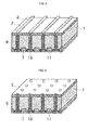
- FIG 4 a schematic plan view of the back surface side electrode structure common to a so-called back-contact type photovoltaic cell element as another embodiment of the present invention is shown in Figure 4 , and perspective views showing outlined structures of photovoltaic cell elements, which are different embodiments of a back-contact type photovoltaic cell element, in Figure 5, Figure 6 and Figure 7 respectively.
- Figure 5, Figure 6 and Figure 7 are perspective views along the AA cross-section in Figure 4 .
- a photovoltaic cell element having a structure shown in the perspective view of Figure 5
- through-holes are formed through the semiconductor substrate 1 penetrating both the light receiving surface side and the back surface side by laser drilling, etching, or the like.
- a texture (not illustrated) that enhances the light incidence efficiency is formed.
- an n + diffusion layer 2 is formed by means of an n type diffusion treatment and an antireflection film (not illustrated) is formed on the n + diffusion layer 2. They can be formed by the same process as for a conventional crystalline silicon type photovoltaic cell element.
- the paste composition for an electrode according to the present invention is filled by means of a printing method or an ink jet method, and on the light receiving surface side, similarly the paste composition for an electrode according to the present invention is printed in a grid form, to form a composition layer constituting a through-hole electrode 9 and a light receiving surface collecting electrode 8.
- pastes for filling and for printing pastes having different compositions in terms of viscosity or the like which are optimized to the respective processes are preferably utilized, but both filling and printing may be carried out using a paste having a single composition.
- an n + diffusion layer 2 and a p + diffusion layer 7 are formed on the back surface side.
- boron (B) or aluminum (Al) is used as an impurity element forming a p + diffusion layer 7.
- the p + diffusion layer 7 may be formed for example by exercising a thermal diffusing treatment using boron as a diffusion source in a production process of a photovoltaic cell element before forming the antireflection coating; or in a case in which aluminum is used, it may be formed by printing and sintering an aluminum paste on the opposite surface side in the printing process.
- back surface electrodes 10 and 11 are formed by printing the paste composition for an electrode according to the present invention in a stripe form on an n + diffusion layer 2 and a p + diffusion layer 7 respectively.
- back surface electrodes may be formed in such a manner that the paste composition for an electrode is used only on the n + diffusion layer 2 side.
- a light receiving surface collecting electrode 8, a through-hole electrode 9, and back surface electrodes 10, 11 are formed.
- the aluminum paste is printed and sintered to form either of the back surface electrodes in advance, and then the paste composition for an electrode may be printed or filled and sintered to form a light receiving surface collecting electrode 8, a through-hole electrode 9, and the other back surface electrode.
- a photovoltaic cell element having a structure shown in a perspective view of Figure 6 can be produced in the same manner as the photovoltaic cell element having a structure shown in a perspective view of Figure 5 , except that a light receiving surface collecting electrode is not formed.
- the paste composition for an electrode according to the present invention can be used for a through-hole electrode 9 and back surface electrodes 10, 11.
- a photovoltaic cell element having a structure shown in a perspective view of Figure 7 can be formed in the same manner as the photovoltaic cell element having a structure shown in a perspective view of Figure 5 , except that an n-type silicon substrate is used as a basic semiconductor substrate, and a through-hole is not formed.
- the paste composition for an electrode according to the present invention can be used for back surface electrodes 10, 11.
- the application of the paste composition for an electrode is not limited to a photovoltaic cell electrode as described above, and it may be favorably applied also to electrode wiring and shield wiring for a plasma display, a ceramic capacitor, an antenna circuit, various sensor circuits, a heat radiating material for a semiconductor device, etc. Among them, it can be used favorably especially for forming an electrode on a substrate containing silicon.
- a photovoltaic cell according to the present invention is constituted by including: at least one photovoltaic cell element mentioned above; and a wiring material is provided on an electrode of the photovoltaic cell element.
- the photovoltaic cell may be also constituted by including plural photovoltaic cell elements connected by means of a wiring material, and may be encapsulated using an encapsulation material. There is no particular restriction on the wiring material and the encapsulation material, and any one may be selected from those used commonly in the art.
- a phosphorus-containing copper alloy containing 7% by mass of phosphorus was prepared according to a conventional method, dissolved and pulverized by a water atomization process, followed by dying and classification. The classified powders were blended, and subjected to deoxigenation and dehydration treatments, thereby producing a phosphorus-containing copper alloy particle containing 7% by mass of phosphorus.
- the average particle diameter (D50%) of the phosphorus-containing copper alloy particle was 5.0 ⁇ m and the shape thereof was approximately spherical.
- the shape of the phosphorus-containing copper alloy particle was judged by observation with a scanning electron microscope (TM-1000, manufactured by Hitachi High-Technologies Corporation).
- the average particle diameter of the phosphorus-containing copper alloy particle was calculated with a laser diffraction average particle diameter analyzer (measurement wave length: 632 nm, LS 13 320, manufactured by Beckman Coulter, Inc.).
- a glass composed of silicon dioxide (SiO 2 ) 3 parts, lead oxide (PbO) 60 parts, boron oxide (B 2 O 3 ) 18 parts, bismuth oxide (Bi 2 O 3 ) 5 parts, aluminum oxide (Al 2 O 3 ) 5 parts, and zinc oxide (ZnO) 9 parts was prepared.
- the obtained glass G01 had a softening point of 420°C, and a crystallization temperature thereof was higher than 650°C.
- a glass G01 particle with an average particle diameter (D50%) of 2.5 ⁇ m was produced.
- the shape thereof was approximately spherical.
- the glass particle shape was judged by observation with a scanning electron microscope (TM-1000, manufactured by Hitachi High-Technologies Corporation).
- the average particle diameter of the glass particle was calculated by using a laser diffraction average particle diameter analyzer (measurement wave length: 632 nm, LS 13 320, manufactured by Beckman Coulter, Inc.).
- the softening point of the glass particle was determined by a differential thermal (DTA) curve obtained by using DTG-60H TG/DTA Simultaneous Measuring Instrument (manufactured by Shimadzu Corporation).
- a tin particle Sn; average particle diameter (D50%) of 5.0 ⁇ m; purity of 99.9%
- Ni average particle diameter (D50%) of 5.0 ⁇ m; purity of 99.9%) 22.8 parts
- the glass G01 particle 7.8 parts, diethylene glycol monobutyl ether (BC) 11.7 parts and ethyl polyacrylate (EPA) 2.2 parts were blended,
- a p-type semiconductor substrate with a thickness of 190 ⁇ m, which had an n + diffusion layer, a texture and an antireflection coating (silicon nitride film) formed on the light receiving surface thereof was prepared, and a specimen in a size of 125 mm ⁇ 125 mm was cut out therefrom.
- the paste composition 1 for an electrode obtained as above was printed by a screen printing method to form an electrode pattern as shown in Figure 2 .
- the electrode pattern was constituted of 150 ⁇ m-wide finger lines and 1.5 mm-wide bus bars, and the printing conditions (screen mesh size, printing speed, and printing pressure) were adjusted appropriately to obtain a layer thickness after sintering of 20 ⁇ m.
- the specimen was then placed in an oven heated to 150°C for 15 minutes to evaporate off the solvent.
- the paste composition 1 for an electrode and an aluminum electrode paste were printed similarly as above by a screen printing method, thereby forming an electrode pattern as shown in Figure 3 .
- the pattern of the back surface power output electrode formed from the paste composition 1 for an electrode was of 123 mm ⁇ 5 mm, and printed at 2 places in total.
- the printing conditions (screen mesh size, printing speed, and printing pressure) were adjusted appropriately to obtain a layer thickness of the back surface power output electrode after sintering of 20 ⁇ m.
- the aluminum electrode paste was printed on the entire surface except the back surface power output electrode, to thereby form a back surface collecting electrode pattern.
- the printing conditions of the aluminum electrode paste were adjusted appropriately to obtain a layer thickness of the back surface collecting electrode after sintering of 30 ⁇ m.
- the specimen was placed in an oven heated to 150°C for 15 minutes to evaporate off the solvent.
- a heat treatment was conducted using a tunnel oven (1-line W/B conveyor tunnel furnace, by Noritake Co., Limited) in the atmosphere for the retention time of 10 seconds with a maximum sintering temperature of 800°C, thereby producing a photovoltaic cell element 1 having desired electrodes.
- a photovoltaic cell element 2 was produced in the same manner as Example 1, except that the sintering condition for forming electrodes was changed from 10 seconds with a maximum temperature of 800°C in Example 1 to 8 seconds with a maximum temperature of 850°C.
- a photovoltaic cell element 3 was produced using a paste composition 3 for an electrode in the same manner as Example 1, except that the phosphorus content of the phosphorus-containing copper alloy particle was changed from 7% by mass in Example 1 to 6% by mass.
- a photovoltaic cell element 4 was produced using a paste composition 4 for an electrode in the same manner as Example 1, except that the phosphorus content of the phosphorus-containing copper alloy particle was changed from 7% by mass in Example 1 to 8% by mass.
- a photovoltaic cell element 5 was produced using a paste composition 5 for an electrode in the same manner as Example 1, except that the sintering condition for forming electrodes was changed from 10 seconds with a maximum temperature of 800°C in Example 1 to 8 seconds with a maximum temperature of 850°C.
- a photovoltaic cell element 6 was produced using a paste composition 6 for an electrode in the same manner as Example 1, except that the average particle diameter (D50%) of the phosphorus-containing copper alloy particle was changed from 5.0 ⁇ m in Example 1 to 1.5 ⁇ m.
- a photovoltaic cell element 7 was produced using a paste composition 7 for an electrode in the same manner as Example 1, except that the contents of the phosphorus-containing copper alloy particle, the tin-containing particle and the nickel-containing particle in Example 1 were changed to the content of the phosphorus-containing copper alloy particle of 36.5 parts, the content of the tin-containing particle of 25.4 parts, and the content of the nickel-containing particle of 16.4 parts.
- a photovoltaic cell element 8 was produced using a paste composition 8 for an electrode in the same manner as Example 1, except that the contents of the phosphorus-containing copper alloy particle, the tin-containing particle and the nickel-containing particle in Example 1 were changed to the contents of the phosphorus-containing copper alloy particle of 46.5 parts, the content of the tin-containing particle of 9.4 parts, and the content of the nickel-containing particle of 22.4 parts.
- a photovoltaic cell element 9 was produced using a paste composition 9 for an electrode in the same manner as Example 1, except that as the tin-containing particle, a tin alloy particle composed of Sn-4Ag-0.5Cu (Sn alloy containing 4% by mass of Ag and 0.5% by mass of Cu) was used instead of the tin particle (Sn) used in Example 1, and the average particle diameter (D50%) thereof was 8.0 ⁇ m.
- a tin alloy particle composed of Sn-4Ag-0.5Cu Sn alloy containing 4% by mass of Ag and 0.5% by mass of Cu
- a photovoltaic cell element 10 was produced using a paste composition 10 for an electrode in the same manner as Example 1, except that as the nickel-containing particle, a nickel alloy particle composed of Ni-60Cu (Ni alloy containing 60% by mass of Cu) was used instead of the nickel particle (Ni) used in Example 1, and the average particle diameter (D50%) thereof was 7.0 ⁇ m.
- a nickel alloy particle composed of Ni-60Cu Ni alloy containing 60% by mass of Cu
- a photovoltaic cell element 11 was produced using a paste composition 11 for an electrode in the same manner as Example 1, except that the average particle diameter (D50%) of the nickel-containing particle (Ni) was changed from 5.0 ⁇ m in Example 1 to 10.0 ⁇ m.
- a silver particle (Ag; average particle diameter (D50%) 3.0 ⁇ m; purity 99.5%) was added. More specifically, a photovoltaic cell element 12 was produced using a paste composition 12 for an electrode in the same manner as Example 1, except that the contents of the respective ingredients were changed to 32.3 parts for the phosphorus-containing copper alloy particle, 21.8 parts for the tin particle, 20.2 parts for the nickel particle, 4.0 parts for the silver particle, 7.8 parts for the glass G01 particle, 11.7 parts for diethylene glycol monobutyl ether (BC), and 2.2 parts for ethyl polyacrylate (EPA).
- BC diethylene glycol monobutyl ether
- EPA ethyl polyacrylate
- Example 1 The content of the glass G01 particle used in Example 1 was changed. More specifically, a photovoltaic cell element 13 was produced using a paste composition 13 for an electrode in the same manner as Example 1, except that the contents of the respective ingredients were changed to 34.3 parts for the phosphorus-containing copper alloy particle, 23.7 parts for the tin particle, 23.2 parts for the nickel particle, 4.9 parts for the glass G01 particle, 11.7 parts for diethylene glycol monobutyl ether (BC), and 2.2 parts for ethyl polyacrylate (EPA).
- BC diethylene glycol monobutyl ether
- EPA ethyl polyacrylate
- a photovoltaic cell element 14 was produced using a paste composition 14 for an electrode in the same manner as Example 1, except that the composition of the glass particle was changed from the glass G01 used in Example 1 to a glass G02 described below.
- the glass G02 was prepared to have a composition of vanadium oxide (V 2 O 5 ) 45 parts, phosphorus oxide (P 2 O 5 ) 24.2 parts, barium oxide (BaO) 20.8 parts, antimony oxide (Sb 2 O 3 ) 5 parts, and tungsten oxide (WO 3 ) 5 parts.
- the softening point of the glass G02 was 492°C, and the crystallization initiation temperature thereof was higher than 650°C.
- G02 particle with an average particle diameter (D50%) of 2.5 ⁇ m was prepared.
- the shape thereof was approximately spherical.
- Example 1 The solvent used in Example 1 was changed from diethylene glycol monobutyl ether to terpineol (Ter) and the resin was changed from polyacrylate to ethyl cellulose (EC), respectively. More specifically, a photovoltaic cell element 15 was produced using a paste composition 15 for an electrode in the same manner as Example 1, except that the contents of the respective ingredients were changed to 33.3 parts for the phosphorus-containing copper alloy particle, 22.8 parts for the tin particle, 22.2 parts for the nickel particle, 7.8 parts for the glass G01 particle, 13.5 parts for terpineol (Ter) and 0.4 parts for ethyl cellulose (EC).
- Paste compositions 16 to 20 for an electrode were prepared in the same manner as Example 1, except that the phosphorus content, average particle diameter (D50%) and content of the phosphorus-containing copper alloy particle, the composition, average particle diameter (D50%) and content of the tin-containing particle, the composition, average particle diameter (D50%) and content of the nickel-containing particle, the content of the silver particle, the type and content of the glass particle, the type and content of the solvent, and the type and content of the resin used in Example 1 were changed as shown in Table 1 and Table 2.
- photovoltaic cell elements 16 to 20 provided with desired electrodes were produced in the same manner as Example 1, respectively, except that the respective obtained paste compositions 16 to 20 for an electrode were used, and the temperature and treatment time of the heat treatment were changed as shown in Table 1 and Table 2.
- a p-type semiconductor substrate having a thickness of 190 ⁇ m and having an n + diffusion layer, a texture and an antireflection coating (silicon nitride film) formed on the light receiving surface thereof was prepared, and a specimen in a size of 125 mm ⁇ 125 mm was cut out therefrom. Then, on the back surface, an aluminum electrode paste was printed to form a back surface collecting electrode pattern. The back surface collecting electrode pattern was printed on the entire surface except the back surface power output electrode as shown in Figure 3 . The printing conditions of the aluminum electrode paste were adjusted appropriately to obtain a layer thickness of the back surface collecting electrode after sintering of 30 ⁇ m. The specimen was placed in an oven heated to 150°C for 15 minutes to evaporate off the solvent.
- a heat treatment was conducted using a tunnel oven (1-line W/B conveyor tunnel furnace, by Noritake Co., Limited) in the atmosphere for the retention time of 10 seconds with a maximum sintering temperature of 800°C, thereby producing a back surface collecting electrode and a p + diffusion layer.
- the paste composition 1 for an electrode obtained as above was printed to form electrode patterns as shown in Figure 2 and Figure 3 .
- the electrode pattern on the light receiving surface was constituted of 150 ⁇ m-wide finger lines and 1.5 mm-wide bus bars, and the printing conditions (screen mesh size, printing speed, and printing pressure) were adjusted appropriately to obtain the layer thickness after sintering of 20 ⁇ m.
- the pattern of the back surface electrode was constituted of 123 mm ⁇ 5 mm and printed at total 2 places with a layer thickness of 20 ⁇ m. The specimen was placed in an oven heated to 150°C for 15 minutes to evaporate off the solvent.
- the specimen was subjected to a heat treatment (sintering) using a tunnel oven (1-line W/B conveyor tunnel furnace, by Noritake Co., Limited) in the atmosphere for the retention time of 10 seconds with a maximum sintering temperature of 650°C, thereby producing a photovoltaic cell element 21 provided with desired electrodes.
- a heat treatment sintering
- a tunnel oven (1-line W/B conveyor tunnel furnace, by Noritake Co., Limited
- a photovoltaic cell element 22 was produced in the same manner as Example 21, except that the paste composition 3 for an electrode obtained as above was used for forming the light receiving surface electrode and the back surface power output electrode.
- a photovoltaic cell element 23 was produced in the same manner as Example 21, except that the paste composition 9 for an electrode obtained as above was used for forming the light receiving surface electrode and the back surface power output electrode, and that the sintering condition for forming the electrodes was changed from 10 seconds with a maximum temperature of 650°C to 10 seconds with a maximum temperature of 620°C.
- a photovoltaic cell element 24 having a structure as shown in Figure 5 was produced.
- a specific production method will be described below. Firstly, through-holes with diameters of 100 ⁇ m were formed in the p-type silicon substrate, which penetrated both the light receiving surface side and the back surface side, using a laser drill. Then, on the light receiving surface side, a texture, an n + diffusion layer, and an antireflection coating were formed successively. In this regard, the n + diffusion layer was also formed in the through-holes, and on a part of the back surface respectively. Then, the paste composition 1 for an electrode was filled in the preformed through-holes by an ink jet method and additionally printed on the light receiving surface side in a grid form.
- a pattern as shown in Figure 4 was printed in a stripe form using the paste composition 1 for an electrode, so that the paste composition for an electrode layer was printed below the through-holes.
- An aluminum electrode paste was printed on the region other than the layer formed from the paste composition for an electrode, thereby forming an aluminum electrode paste layer.
- the specimen was subjected to a heat treatment using a tunnel oven (1-line W/B conveyor tunnel furnace, by Noritake Co., Limited) in the atmosphere for the retention time of 10 seconds with a maximum sintering temperature of 800°C, thereby producing a photovoltaic cell element 24 provided with desired electrodes.
- a p + diffusion layer was formed by the diffusion of Al into the p-type silicon substrate by sintering.
- a photovoltaic cell element 25 was produced in the same manner as Example 24, except that the paste composition 1 for an electrode used in Example 24 was changed to the paste composition 16 for an electrode obtained as above to form the light receiving surface collecting electrode, the through-hole electrode, and the back surface electrode.
- a photovoltaic cell element 26 was produced in the same manner as Example 24, except that the sintering condition for forming electrodes was changed from 10 seconds with a maximum temperature of 800°C to 8 seconds with a maximum temperature of 850°C.
- a photovoltaic cell element 27 was produced in the same manner as Example 24, except that the paste composition 1 for an electrode used in Example 24 was changed to the paste composition 9 for an electrode obtained as above to form the light receiving surface collecting electrode, the through-hole electrode, and the back surface electrode.
- a paste composition 28 for an electrode was prepared in the same manner as Example 1, except that the glass particle was changed from the glass G01 particle used in Example 1 to a glass G03 particle.
- the glass G03 was prepared to have a composition of silicon dioxide (SiO 2 ) 13 parts, boron oxide (B 2 O 3 ) 58 parts, zinc oxide (ZnO) 38 parts, aluminum oxide (Al 2 O 3 ) 12 parts, and barium oxide (BaO) 12 parts.
- the softening point of the obtained glass G03 was 583°C, and the crystallization temperature thereof was higher than 650°C.
- the glass G03 particle with an average particle diameter (D50%) of 2.5 ⁇ m was obtained.
- the shape thereof was approximately spherical.
- a photovoltaic cell element 28 having a structure as shown in Figure 6 was produced.
- the production method was the same as Examples 24 to 27 except that the light receiving surface electrode was not formed.
- the retention time was 10 seconds with a maximum temperature of 800°C.
- a photovoltaic cell element 29 was produced in the same manner as Example 28, except that the sintering condition for forming an electrode was changed from 10 seconds with a maximum temperature of 800°C to 8 seconds with a maximum temperature of 850°C.
- a photovoltaic cell element 30 having a structure as shown in Figure 7 was produced.
- the production method was the same as Example 24 except that an n-type silicon substrate was used as a basic substrate, and that the light receiving surface electrode, the through-holes and the through-hole electrode were not formed.
- the retention time was 10 seconds with a maximum temperature of 800°C.
- a paste composition 31 for an electrode was prepared in the same manner as Example 5, except that the glass particle was changed from the glass G01 particle used in Example 9 to the glass G03 particle. Using this, a photovoltaic cell element 31 having a structure as shown in Figure 7 was produced in the same manner as Example 30.
- a paste composition 32 for an electrode was prepared in the same manner as Example 16, except that the glass particle was changed from the glass G01 particle used in Example 12 to the glass G03 particle. Using this, a photovoltaic cell element 32 having a structure as shown in Figure 7 was produced in the same manner as Example 30.
- a paste composition C1 for an electrode was prepared in the same manner as Example 1, except that the phosphorus-containing copper alloy particle, the tin-containing particle and the nickel-containing particle used in the preparation of the paste composition for an electrode in Example 1 were not used, and that the respective ingredients were changed to have the composition as shown in Table 1 and Table 2.
- a photovoltaic cell element C1 was produced in the same manner as Example 1 except that the paste composition C1 for an electrode not containing the phosphorus-containing copper alloy particle, the tin-containing particle and the nickel-containing particle was used.
- Paste compositions C2 to C4 for an electrode having the compositions shown in Table 1 and Table 2 were prepared except that a phosphorus-containing copper alloy particle having a different phosphorus content was used, and that no tin-containing particle and no nickel-containing particle were used in the preparation of the paste composition for an electrode in Example 1.
- Photovoltaic cell elements C2 to C4 were produced in the same manner as in Comparative Example 1 respectively, except that the respective paste compositions C2 to C4 for an electrode were used.
- a paste composition C5 for an electrode was prepared in the same manner as Example 1, except that a copper particle (purity 99.5%; average particle diameter (D50%) 5.0 ⁇ m; content 33.3 parts) was used instead of the phosphorus-containing copper alloy particle used in the preparation of the paste composition for an electrode in Example 1, and the compositions of the respective ingredients were changed as shown in Table 1 and Table 2.
- a photovoltaic cell element C5 was produced in the same manner as in Comparative Example 1, except that the paste composition C5 for an electrode was used.
- a photovoltaic cell element C6 was produced in the same manner as Example 24, except that the paste composition 1 for an electrode used in Example 24 was changed to the paste composition C1 for an electrode obtained as above to form a light receiving surface collecting electrode, a through-hole electrode, and a back surface electrode were formed.
- a photovoltaic cell element C7 was produced in the same manner as Example 28, except that the paste composition 28 for an electrode used in Example 28 was changed to the paste composition C1 for an electrode obtained as above.
- a photovoltaic cell element C8 was produced in the same manner as Example 30, except that the paste composition 28 for an electrode used in Example 30 was changed to the paste composition C1 for an electrode obtained as above.
- a cross-section of a light-receiving surface electrode formed by baking the prepared paste composition for an electrode was observed by a scanning electron microscope Miniscope TM-1000 (by Hitachi, Ltd.) with the acceleration voltage of 15 kV, to examine existence or nonexistence of a Cu-Sn alloy phase, a Cu-Sn-Ni alloy phase, and an Sn-P-O glass phase in an electrode, as well as a formed location of a Sn-P-O glass phase.
- Table 3 Examples Electricity generation performance as photovoltaic cell Observation result of electrode cross-section structure Jsc (relative value) short circuit current Voc (relative value) open-circuit voltage F.F.
- Comparative Examples 3 to 5 the electricity generation performance deteriorated compared to Comparative Example 1. The above was apparently caused by the following.
- Comparative Example 4 since a tin-containing particle was not included, interdiffusion of a silicon substrate and copper took place during baking and the pn-junction quality in the substrate seemingly deteriorated.
- Comparative Example 5 since a phosphorus-containing copper alloy particle was not used and pure copper (phosphorus content was 0% by mass) was used, the copper particle was oxidized during baking before reacting with a tin-containing particle and therefore a Cu-Sn alloy phase was not formed, and seemingly the electrode resistivity increased.
- the electricity generation performances of the photovoltaic cell elements produced in Examples 1 to 23 were more or less same as the found value for the photovoltaic cell element according to Comparative Example 1.
- the photovoltaic cell elements 21 to 23 although paste compositions for an electrode were baked at a relatively low temperature (620°C to 650°C), high electricity generation performances were exhibited.
- a Cu-Sn-Ni alloy phase or both of a Cu-Sn-Ni alloy phase and a Cu-Sn, and an Sn-P-O glass phase were present and the Sn-P-O glass phase was formed between the Cu-Sn alloy phase and the Cu-Sn-Ni alloy phase and the silicon substrate.
- the electricity generation performances of the photovoltaic cell elements produced in Examples 24 to 27 were more or less same as the photovoltaic cell element according to Comparative Example 6.
- a Cu-Sn-Ni alloy phase and an Sn-P-O glass phase were present and the Sn-P-O glass phase was formed between the Cu-Sn-Ni alloy phase and the silicon substrate.
- the electricity generation performances of the photovoltaic cell elements produced in Examples 28 to 29 were more or less same as the photovoltaic cell element according to Comparative Example 7.
- a Cu-Sn-Ni alloy phase and an Sn-P-O glass phase were present and the Sn-P-O glass phase was formed between the Cu-Sn-Ni alloy phase and the silicon substrate.
- the electricity generation performances of the photovoltaic cell elements produced in Examples 30 to 32 were more or less same as the photovoltaic cell element according to Comparative Example 8.
- a Cu-Sn-Ni alloy phase and an Sn-P-O glass phase were present and the Sn-P-O glass phase was formed between the Cu-Sn-Ni alloy phase and the silicon substrate.
Landscapes
- Chemical & Material Sciences (AREA)
- Engineering & Computer Science (AREA)
- Materials Engineering (AREA)
- Organic Chemistry (AREA)
- Mechanical Engineering (AREA)
- Metallurgy (AREA)
- Spectroscopy & Molecular Physics (AREA)
- Dispersion Chemistry (AREA)
- Physics & Mathematics (AREA)
- Life Sciences & Earth Sciences (AREA)
- Chemical Kinetics & Catalysis (AREA)
- General Chemical & Material Sciences (AREA)
- Geochemistry & Mineralogy (AREA)
- Conductive Materials (AREA)
- Photovoltaic Devices (AREA)
- Sustainable Energy (AREA)
- Sustainable Development (AREA)
- Powder Metallurgy (AREA)
- Electrodes Of Semiconductors (AREA)
Applications Claiming Priority (2)
| Application Number | Priority Date | Filing Date | Title |
|---|---|---|---|
| JP2011249120 | 2011-11-14 | ||
| PCT/JP2012/079157 WO2013073478A1 (ja) | 2011-11-14 | 2012-11-09 | 電極用ペースト組成物、太陽電池素子及び太陽電池 |
Publications (2)
| Publication Number | Publication Date |
|---|---|
| EP2782102A1 true EP2782102A1 (de) | 2014-09-24 |
| EP2782102A4 EP2782102A4 (de) | 2015-07-15 |
Family
ID=48429538
Family Applications (1)
| Application Number | Title | Priority Date | Filing Date |
|---|---|---|---|
| EP12849394.7A Withdrawn EP2782102A4 (de) | 2011-11-14 | 2012-11-09 | Elektrodenpastenzusammensetzung, solarzellenelement und solarzelle |
Country Status (6)
| Country | Link |
|---|---|
| EP (1) | EP2782102A4 (de) |
| JP (2) | JP5811186B2 (de) |
| KR (2) | KR20150125956A (de) |
| CN (1) | CN103930950A (de) |
| TW (1) | TW201324539A (de) |
| WO (1) | WO2013073478A1 (de) |
Cited By (2)
| Publication number | Priority date | Publication date | Assignee | Title |
|---|---|---|---|---|
| EP3614399A1 (de) | 2018-08-23 | 2020-02-26 | Centrum Badan i Rozwoju Technologii dla Przemyslu S.A. | Verfahren zur herstellung von modifizierten elektrisch leitfähigen kupferpartikeln und daraus hergestellte modifizierte elektrisch leitfähige kupferpartikel |
| EP3805666A4 (de) * | 2018-06-04 | 2022-02-23 | Csic Pride (Nanjing) Cryogenic Technology Co., Ltd. | Kältespeichermaterial und kryogener kühlschrank vom kältespeichertyp mit verwendung davon |
Families Citing this family (11)
| Publication number | Priority date | Publication date | Assignee | Title |
|---|---|---|---|---|
| TWI480357B (zh) | 2013-12-17 | 2015-04-11 | 財團法人工業技術研究院 | 導電膠組成物與電極的形成方法 |
| TWI634668B (zh) * | 2013-12-19 | 2018-09-01 | 日商日立化成股份有限公司 | 太陽電池以及太陽電池模組 |
| WO2015092901A1 (ja) * | 2013-12-19 | 2015-06-25 | 日立化成株式会社 | 電極接続セット、太陽電池の製造方法、太陽電池及び太陽電池モジュール |
| WO2015092900A1 (ja) * | 2013-12-19 | 2015-06-25 | 日立化成株式会社 | 太陽電池及び太陽電池モジュール |
| JP2015164171A (ja) * | 2014-01-31 | 2015-09-10 | 日立化成株式会社 | 太陽電池、太陽電池モジュール、電極付部品、半導体装置及び電子部品 |
| CN105934830B (zh) * | 2014-01-31 | 2018-09-11 | 日立化成株式会社 | 电极形成用组合物、电极、太阳能电池元件及其制造方法以及太阳能电池 |
| JP6464669B2 (ja) * | 2014-02-12 | 2019-02-06 | 日立化成株式会社 | 電極形成用組成物、電極、太陽電池素子並びに太陽電池及びその製造方法 |
| JP6617427B2 (ja) * | 2015-03-30 | 2019-12-11 | 日立化成株式会社 | 電極形成用組成物、電極、太陽電池素子及びその製造方法並びに太陽電池 |
| WO2017163498A1 (ja) * | 2016-03-23 | 2017-09-28 | 三菱電機株式会社 | 太陽電池、および、太陽電池の製造方法 |
| CN109970347A (zh) * | 2019-04-29 | 2019-07-05 | 齐鲁工业大学 | 一种提高锂离子电池性能的TeO2-V2O5-CuO微晶玻璃负极材料 |
| CN118136305B (zh) * | 2024-02-29 | 2024-11-08 | 佛山市中科兴新材料有限公司 | 一种导电浆料及其应用 |
Family Cites Families (15)
| Publication number | Priority date | Publication date | Assignee | Title |
|---|---|---|---|---|
| JPS63118466A (ja) | 1986-11-04 | 1988-05-23 | 富士変速機株式会社 | 横行格納台車の横行駆動装置 |
| JP4244466B2 (ja) * | 1999-10-13 | 2009-03-25 | 株式会社村田製作所 | 導電性ペーストおよびそれを用いた半導体セラミック電子部品 |
| JP2004217952A (ja) | 2003-01-09 | 2004-08-05 | Mitsui Mining & Smelting Co Ltd | 表面処理銅粉並びにその表面処理銅粉の製造方法及びその表面処理銅粉を用いた導電性ペースト |
| JP4868716B2 (ja) | 2004-04-28 | 2012-02-01 | 三井金属鉱業株式会社 | フレーク銅粉及び導電性ペースト |
| US7494607B2 (en) | 2005-04-14 | 2009-02-24 | E.I. Du Pont De Nemours And Company | Electroconductive thick film composition(s), electrode(s), and semiconductor device(s) formed therefrom |
| US8575474B2 (en) * | 2006-03-20 | 2013-11-05 | Heracus Precious Metals North America Conshohocken LLC | Solar cell contacts containing aluminum and at least one of boron, titanium, nickel, tin, silver, gallium, zinc, indium and copper |
| WO2008078374A1 (ja) * | 2006-12-25 | 2008-07-03 | Namics Corporation | 太陽電池用導電性ペースト |
| JP5156328B2 (ja) * | 2007-10-18 | 2013-03-06 | 福田金属箔粉工業株式会社 | 導電材ペースト用銅合金粉 |
| JP4709238B2 (ja) | 2008-02-08 | 2011-06-22 | 株式会社日立製作所 | Cu系配線用材料およびそれを用いた電子部品 |
| US20090266409A1 (en) * | 2008-04-28 | 2009-10-29 | E.I.Du Pont De Nemours And Company | Conductive compositions and processes for use in the manufacture of semiconductor devices |
| JP2011171270A (ja) * | 2010-01-25 | 2011-09-01 | Hitachi Chem Co Ltd | 電極用ペースト組成物および太陽電池 |
| US20110180139A1 (en) * | 2010-01-25 | 2011-07-28 | Hitachi Chemical Company, Ltd. | Paste composition for electrode and photovoltaic cell |
| JP5633285B2 (ja) * | 2010-01-25 | 2014-12-03 | 日立化成株式会社 | 電極用ペースト組成物及び太陽電池 |
| JP5633286B2 (ja) * | 2010-01-25 | 2014-12-03 | 日立化成株式会社 | 電極用ペースト組成物および太陽電池 |
| JP2011249120A (ja) | 2010-05-26 | 2011-12-08 | Rohm Co Ltd | 照明装置 |
-
2012
- 2012-11-09 KR KR1020157025242A patent/KR20150125956A/ko not_active Ceased
- 2012-11-09 WO PCT/JP2012/079157 patent/WO2013073478A1/ja not_active Ceased
- 2012-11-09 KR KR1020147013653A patent/KR20140082835A/ko not_active Abandoned
- 2012-11-09 EP EP12849394.7A patent/EP2782102A4/de not_active Withdrawn
- 2012-11-09 JP JP2013544250A patent/JP5811186B2/ja not_active Expired - Fee Related
- 2012-11-09 CN CN201280055775.8A patent/CN103930950A/zh active Pending
- 2012-11-13 TW TW101142290A patent/TW201324539A/zh unknown
-
2015
- 2015-07-27 JP JP2015148112A patent/JP2016001612A/ja active Pending
Cited By (3)
| Publication number | Priority date | Publication date | Assignee | Title |
|---|---|---|---|---|
| EP3805666A4 (de) * | 2018-06-04 | 2022-02-23 | Csic Pride (Nanjing) Cryogenic Technology Co., Ltd. | Kältespeichermaterial und kryogener kühlschrank vom kältespeichertyp mit verwendung davon |
| EP3614399A1 (de) | 2018-08-23 | 2020-02-26 | Centrum Badan i Rozwoju Technologii dla Przemyslu S.A. | Verfahren zur herstellung von modifizierten elektrisch leitfähigen kupferpartikeln und daraus hergestellte modifizierte elektrisch leitfähige kupferpartikel |
| WO2020039007A1 (en) | 2018-08-23 | 2020-02-27 | Centrum Badan I Rozwoju Technologii Dla Przemyslu S.A. | A method for manufacturing modified electrically-conductive copper particles and modified electrically-conductive copper particles manufactured thereof |
Also Published As
| Publication number | Publication date |
|---|---|
| JP2016001612A (ja) | 2016-01-07 |
| JPWO2013073478A1 (ja) | 2015-04-02 |
| TW201324539A (zh) | 2013-06-16 |
| EP2782102A4 (de) | 2015-07-15 |
| KR20140082835A (ko) | 2014-07-02 |
| WO2013073478A1 (ja) | 2013-05-23 |
| KR20150125956A (ko) | 2015-11-10 |
| CN103930950A (zh) | 2014-07-16 |
| JP5811186B2 (ja) | 2015-11-11 |
Similar Documents
| Publication | Publication Date | Title |
|---|---|---|
| EP2782102A1 (de) | Elektrodenpastenzusammensetzung, solarzellenelement und solarzelle | |
| JP5768455B2 (ja) | 電極用ペースト組成物及び太陽電池素子 | |
| KR101350098B1 (ko) | 전극용 페이스트 조성물 및 태양 전지 | |
| JP6206491B2 (ja) | 電極形成用組成物、太陽電池素子及び太陽電池 | |
| WO2012140787A1 (ja) | 電極用ペースト組成物、太陽電池素子及び太陽電池 | |
| JP5891599B2 (ja) | シリコン系太陽電池の電極用ペースト組成物 | |
| US20120260981A1 (en) | Paste composition for electrode, photovoltaic cell element, and photovoltaic cell | |
| JP5879793B2 (ja) | 素子の製造方法及び太陽電池の製造方法 | |
| US20130118573A1 (en) | Paste composition for electrode, photovoltaic cell element, and photovoltaic cell | |
| JP5720393B2 (ja) | 電極用ペースト組成物、太陽電池素子及び太陽電池 | |
| JP5772174B2 (ja) | 素子及び太陽電池並びに電極用ペースト組成物 | |
| US20120260982A1 (en) | Paste composition for electrode, photovoltaic cell element, and photovoltaic cell | |
| JP2015188089A (ja) | 素子及び太陽電池 | |
| JP2015195223A (ja) | 電極用ペースト組成物、太陽電池素子及び太陽電池 | |
| JP2015144126A (ja) | 電極用ペースト組成物及び太陽電池素子 | |
| JP5899689B2 (ja) | 素子及び太陽電池 | |
| JP5958526B2 (ja) | 素子及び太陽電池並びに電極用ペースト組成物 | |
| JP2016122840A (ja) | 素子及び太陽電池並びに電極用ペースト組成物 | |
| JP6464669B2 (ja) | 電極形成用組成物、電極、太陽電池素子並びに太陽電池及びその製造方法 | |
| JP2015079975A (ja) | 素子及び太陽電池並びに電極用ペースト組成物 | |
| JP2016054312A (ja) | 素子及び太陽電池 | |
| JP2016189308A (ja) | 電極形成用組成物、電極、太陽電池素子及びその製造方法、並びに太陽電池 |
Legal Events
| Date | Code | Title | Description |
|---|---|---|---|
| PUAI | Public reference made under article 153(3) epc to a published international application that has entered the european phase |
Free format text: ORIGINAL CODE: 0009012 |
|
| 17P | Request for examination filed |
Effective date: 20140527 |
|
| AK | Designated contracting states |
Kind code of ref document: A1 Designated state(s): AL AT BE BG CH CY CZ DE DK EE ES FI FR GB GR HR HU IE IS IT LI LT LU LV MC MK MT NL NO PL PT RO RS SE SI SK SM TR |
|
| DAX | Request for extension of the european patent (deleted) | ||
| RA4 | Supplementary search report drawn up and despatched (corrected) |
Effective date: 20150611 |
|
| RIC1 | Information provided on ipc code assigned before grant |
Ipc: H01L 31/068 20120101ALI20150605BHEP Ipc: H01B 1/22 20060101AFI20150605BHEP Ipc: H01L 31/0224 20060101ALI20150605BHEP |
|
| STAA | Information on the status of an ep patent application or granted ep patent |
Free format text: STATUS: THE APPLICATION IS DEEMED TO BE WITHDRAWN |
|
| 18D | Application deemed to be withdrawn |
Effective date: 20170601 |