EP2781994A2 - Module tactile et appareil électronique - Google Patents
Module tactile et appareil électronique Download PDFInfo
- Publication number
- EP2781994A2 EP2781994A2 EP14159813.6A EP14159813A EP2781994A2 EP 2781994 A2 EP2781994 A2 EP 2781994A2 EP 14159813 A EP14159813 A EP 14159813A EP 2781994 A2 EP2781994 A2 EP 2781994A2
- Authority
- EP
- European Patent Office
- Prior art keywords
- light
- emitting element
- cover
- guide film
- light guide
- Prior art date
- Legal status (The legal status is an assumption and is not a legal conclusion. Google has not performed a legal analysis and makes no representation as to the accuracy of the status listed.)
- Granted
Links
- 239000000463 material Substances 0.000 claims description 8
- 239000000853 adhesive Substances 0.000 claims description 6
- 230000001070 adhesive effect Effects 0.000 claims description 6
- 239000011521 glass Substances 0.000 claims description 2
- 229910000679 solder Inorganic materials 0.000 claims description 2
- 239000010408 film Substances 0.000 description 28
- 230000000694 effects Effects 0.000 description 2
- 238000012986 modification Methods 0.000 description 2
- 230000004048 modification Effects 0.000 description 2
- 229920002799 BoPET Polymers 0.000 description 1
- 239000005041 Mylar™ Substances 0.000 description 1
- 239000004033 plastic Substances 0.000 description 1
- 239000010409 thin film Substances 0.000 description 1
Images


Classifications
-
- G—PHYSICS
- G06—COMPUTING; CALCULATING OR COUNTING
- G06F—ELECTRIC DIGITAL DATA PROCESSING
- G06F3/00—Input arrangements for transferring data to be processed into a form capable of being handled by the computer; Output arrangements for transferring data from processing unit to output unit, e.g. interface arrangements
- G06F3/01—Input arrangements or combined input and output arrangements for interaction between user and computer
- G06F3/03—Arrangements for converting the position or the displacement of a member into a coded form
- G06F3/041—Digitisers, e.g. for touch screens or touch pads, characterised by the transducing means
- G06F3/0412—Digitisers structurally integrated in a display
-
- G—PHYSICS
- G06—COMPUTING; CALCULATING OR COUNTING
- G06F—ELECTRIC DIGITAL DATA PROCESSING
- G06F1/00—Details not covered by groups G06F3/00 - G06F13/00 and G06F21/00
- G06F1/16—Constructional details or arrangements
- G06F1/1613—Constructional details or arrangements for portable computers
- G06F1/1633—Constructional details or arrangements of portable computers not specific to the type of enclosures covered by groups G06F1/1615 - G06F1/1626
- G06F1/1684—Constructional details or arrangements related to integrated I/O peripherals not covered by groups G06F1/1635 - G06F1/1675
- G06F1/169—Constructional details or arrangements related to integrated I/O peripherals not covered by groups G06F1/1635 - G06F1/1675 the I/O peripheral being an integrated pointing device, e.g. trackball in the palm rest area, mini-joystick integrated between keyboard keys, touch pads or touch stripes
-
- G—PHYSICS
- G06—COMPUTING; CALCULATING OR COUNTING
- G06F—ELECTRIC DIGITAL DATA PROCESSING
- G06F3/00—Input arrangements for transferring data to be processed into a form capable of being handled by the computer; Output arrangements for transferring data from processing unit to output unit, e.g. interface arrangements
- G06F3/01—Input arrangements or combined input and output arrangements for interaction between user and computer
- G06F3/03—Arrangements for converting the position or the displacement of a member into a coded form
- G06F3/033—Pointing devices displaced or positioned by the user, e.g. mice, trackballs, pens or joysticks; Accessories therefor
- G06F3/0354—Pointing devices displaced or positioned by the user, e.g. mice, trackballs, pens or joysticks; Accessories therefor with detection of 2D relative movements between the device, or an operating part thereof, and a plane or surface, e.g. 2D mice, trackballs, pens or pucks
- G06F3/03547—Touch pads, in which fingers can move on a surface
-
- H—ELECTRICITY
- H04—ELECTRIC COMMUNICATION TECHNIQUE
- H04M—TELEPHONIC COMMUNICATION
- H04M1/00—Substation equipment, e.g. for use by subscribers
- H04M1/02—Constructional features of telephone sets
- H04M1/0202—Portable telephone sets, e.g. cordless phones, mobile phones or bar type handsets
- H04M1/026—Details of the structure or mounting of specific components
- H04M1/0266—Details of the structure or mounting of specific components for a display module assembly
-
- G—PHYSICS
- G06—COMPUTING; CALCULATING OR COUNTING
- G06F—ELECTRIC DIGITAL DATA PROCESSING
- G06F1/00—Details not covered by groups G06F3/00 - G06F13/00 and G06F21/00
- G06F1/16—Constructional details or arrangements
- G06F1/1613—Constructional details or arrangements for portable computers
- G06F1/1626—Constructional details or arrangements for portable computers with a single-body enclosure integrating a flat display, e.g. Personal Digital Assistants [PDAs]
-
- G—PHYSICS
- G06—COMPUTING; CALCULATING OR COUNTING
- G06F—ELECTRIC DIGITAL DATA PROCESSING
- G06F2203/00—Indexing scheme relating to G06F3/00 - G06F3/048
- G06F2203/033—Indexing scheme relating to G06F3/033
- G06F2203/0339—Touch strips, e.g. orthogonal touch strips to control cursor movement or scrolling; single touch strip to adjust parameter or to implement a row of soft keys
-
- G—PHYSICS
- G06—COMPUTING; CALCULATING OR COUNTING
- G06F—ELECTRIC DIGITAL DATA PROCESSING
- G06F3/00—Input arrangements for transferring data to be processed into a form capable of being handled by the computer; Output arrangements for transferring data from processing unit to output unit, e.g. interface arrangements
- G06F3/01—Input arrangements or combined input and output arrangements for interaction between user and computer
- G06F3/048—Interaction techniques based on graphical user interfaces [GUI]
- G06F3/0487—Interaction techniques based on graphical user interfaces [GUI] using specific features provided by the input device, e.g. functions controlled by the rotation of a mouse with dual sensing arrangements, or of the nature of the input device, e.g. tap gestures based on pressure sensed by a digitiser
- G06F3/0488—Interaction techniques based on graphical user interfaces [GUI] using specific features provided by the input device, e.g. functions controlled by the rotation of a mouse with dual sensing arrangements, or of the nature of the input device, e.g. tap gestures based on pressure sensed by a digitiser using a touch-screen or digitiser, e.g. input of commands through traced gestures
- G06F3/04886—Interaction techniques based on graphical user interfaces [GUI] using specific features provided by the input device, e.g. functions controlled by the rotation of a mouse with dual sensing arrangements, or of the nature of the input device, e.g. tap gestures based on pressure sensed by a digitiser using a touch-screen or digitiser, e.g. input of commands through traced gestures by partitioning the display area of the touch-screen or the surface of the digitising tablet into independently controllable areas, e.g. virtual keyboards or menus
-
- H—ELECTRICITY
- H04—ELECTRIC COMMUNICATION TECHNIQUE
- H04M—TELEPHONIC COMMUNICATION
- H04M1/00—Substation equipment, e.g. for use by subscribers
- H04M1/02—Constructional features of telephone sets
- H04M1/0202—Portable telephone sets, e.g. cordless phones, mobile phones or bar type handsets
- H04M1/026—Details of the structure or mounting of specific components
- H04M1/0274—Details of the structure or mounting of specific components for an electrical connector module
-
- H—ELECTRICITY
- H04—ELECTRIC COMMUNICATION TECHNIQUE
- H04M—TELEPHONIC COMMUNICATION
- H04M1/00—Substation equipment, e.g. for use by subscribers
- H04M1/02—Constructional features of telephone sets
- H04M1/0202—Portable telephone sets, e.g. cordless phones, mobile phones or bar type handsets
- H04M1/026—Details of the structure or mounting of specific components
- H04M1/0277—Details of the structure or mounting of specific components for a printed circuit board assembly
-
- H—ELECTRICITY
- H04—ELECTRIC COMMUNICATION TECHNIQUE
- H04M—TELEPHONIC COMMUNICATION
- H04M1/00—Substation equipment, e.g. for use by subscribers
- H04M1/02—Constructional features of telephone sets
- H04M1/22—Illumination; Arrangements for improving the visibility of characters on dials
-
- H—ELECTRICITY
- H04—ELECTRIC COMMUNICATION TECHNIQUE
- H04M—TELEPHONIC COMMUNICATION
- H04M2250/00—Details of telephonic subscriber devices
- H04M2250/22—Details of telephonic subscriber devices including a touch pad, a touch sensor or a touch detector
Definitions
- the application generally relates to a touch module and an electronic apparatus, and more particularly, to a touch module and an electronic apparatus having a virtual bottom.
- An electronic apparatus with touch sensing functions may compose a virtual bottom by disposing an icon next to a display region and a touch panel at the back. Accordingly, when a user touches the icon, a corresponding region on the touch panel can be driven to generate a touching signal.
- a light-emitting element can be disposed on an additional printed circuit board (PCB) or on a flexible printed circuit board (FPC), so that light emitted by the light-emitting element can be guided to the icon by utilizing a light guide film.
- PCB printed circuit board
- FPC flexible printed circuit board
- the application is directed to a touch module having a smaller volume.
- the application provides an electronic apparatus in which a touch module has a smaller volume.
- the touch module of the application adapted for an electronic apparatus, includes a cover, a touch sensor layer, a flexible printed circuit board, a light-emitting element and a light guide film.
- the cover has at least one transparent icon.
- the touch sensor layer is disposed under the cover.
- the flexible printed circuit board is disposed under the cover and electrically connected to the touch sensor layer.
- the light-emitting element is mounted on the flexible printed circuit board, wherein the flexible printed circuit board is located between the cover and the light-emitting element.
- the light guide film is disposed under the cover, wherein the touch sensor layer is located between the cover and the light guide film. Light emitted by the light-emitting element is transmitted to the transparent icon through the light guide film.
- An electronic apparatus of the application includes above-said touch module and a housing.
- the housing has a housing opening, wherein the cover of the touch module is disposed on the housing and covering the housing opening of the housing, so as to construct an accommodating space with housing.
- the touch sensor layer, the flexible printed circuit board, the light-emitting element and the light guide film of the touch module are located in the accommodating space.
- the touch module can drive the light-emitting element without requiring additional printed circuit board or flexible printed circuit board. Accordingly, volume of the touch module may be reduced, and volume of the electronic apparatus may also be further reduced.
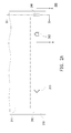
- FIG. 1 is a schematic cross-sectional view of an electronic apparatus according to an embodiment of the application.
- an electronic apparatus 100 includes a touch module 200 adapted for the electronic apparatus 100, and a housing 110.
- the electronic apparatus 100 can be an electronic apparatus having a touch sensing function, such as a cell phone or a tablet computer.
- the touch module 200 includes a cover 210, a touch sensor layer 220, a flexible printed circuit board 230, a light-emitting element 240 and a light guide film 250.
- a material of the cover 210 is, for example, a glass or a plastic
- the light-emitting element 240 is, for example, a light-emitting diode (LED) or other appropriate light-emitting elements.
- the housing 110 has a housing opening 111, and the cover 210 of the touch module 200 is disposed on the housing 110 and covering the housing opening 111 of the housing 110, so as to substantially construct an accommodating space S together with the housing 110.
- the housing 110 is not limited to be composed of single or multiple parts.
- the touch sensor layer 220, the flexible printed circuit board 230, the light-emitting element 240 and the light guide film 250 of the touch module 200 are located in the accommodating space S. A structure design of the touch module 200 is described in detail below with reference to FIG. 2A to FIG. 2D .
- FIG. 2A is a schematic front view of a touch module of the embodiment depicted in FIG. 1 .
- FIG. 2B is a schematic back view of a touch module of the embodiment depicted in FIG. 2A .
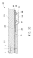
- FIG. 2C is a schematic cross-sectional view of the touch module depicted in FIG. 2A along a line A-A.
- FIG. 2D is a schematic cross-sectional view of the touch module depicted in FIG. 2A along a line B-B.
- the cover 210 of the touch module 200 includes a first region 211, a second region 212 and at least one transparent icon 213, and the transparent icon 213 is located on the second region 212.
- the touch sensor layer 220 is disposed under the cover 210, and the flexible printed circuit board 230 is also disposed under the cover 210 and the flexible printed circuit board 230 is electrically connected to the touch sensor layer 220.
- a plurality of bonding areas BA are provided on the second region 212 of the cover 210, and circuits of the touch sensor layer 220 and the flexible printed circuit board 230 are arranged in said bonding areas, so that the touch sensor layer 220 and the flexible printed circuit board 230 may be electrically connected to each other.
- the light-emitting element 240 is mounted on the flexible printed circuit board 230, and the flexible printed circuit board 230 is located between the cover 210 and the light-emitting element 240. More specifically, in the present embodiment, the flexible printed circuit board 230 includes at least one exposed conductive end EP. A conductive adhesive material EM is provided on the conductive end EP, and the light-emitting element 240 is fixed on the flexible printed circuit board 230 through the conductive adhesive material EM. In the present embodiment, the conductive adhesive material is, for example, a solder. Because the light-emitting element 240 is merely used for providing light that is easily identified for the transparent icon 213, a required power thereof is relatively lower. Therefore, the light-emitting element 240 may be mounted on the flexible printed circuit board 230 without causing damages to the flexible printed circuit board 230 due to overheat.
- the light guide film 250 is also disposed under the cover 210, and the touch sensor layer 220 is located between the cover 210 and the light guide film 250.
- the light-emitting element 240 is adjacent to an edge of the light guide film 250, and light 70 emitted by the light-emitting element 240 can enter the light guide film 250 from the edge of the light guide film 250.
- the touch module 200 further includes a shielding plate 260 covering the light guide film 250 and the light-emitting element 240.
- the shielding plate 260 is, for example, a Mylar thin film having a shielding effect.
- the shielding plate 260 may cover the light guide film 250 and the light-emitting element 240 as well as covering gaps between the light guide film 250 and the light-emitting element 240 at the same time. Accordingly, a possibility for a part of light emitted by the light-emitting element 240 to leak through the gaps between the light guide film 250 and the light-emitting element 240 or other possible leaking regions may be lower, so as to enhance a light-use efficiency.
- the light guide film 250 is a rectangular sheet having two opposite short sides 251 and 253 and two opposite long sides 252 and 254, and the light-emitting element 240 is disposed at an edge adjacent to one of the short sides 251 and 253 of the light guide film 250. Accordingly, as shown in 2B and 2C, the light 70 emitted by the light-emitting element 240 can enter the light guide film 250 from one of the short sides 251 and 253, and be transmitted to the transparent icon 213 through the light guide film 250, so that the transparent icon 213 can be easily identified.
- the electronic apparatus 100 further includes a mainboard 120 and a display module 130.
- the mainboard 120 is disposed in the accommodating space S and electrically connected to the flexible printed circuit board 230.
- the flexible printed circuit board includes a bent portion 232, and the bent portion 232 crosses the display module 130 to connect to the mainboard 120.
- the display module 130 is also disposed in the accommodating space S and electrically connected to the mainboard 120. More specifically, in the present embodiment, the light guide film 250 is located between the display module 130 and the touch sensor layer 220. In addition, as shown in FIG. 2D , the display module 130 has a display region AA, and the display region AA corresponds to the first region 211 of the cover 210. More specifically, in the present embodiment, the display module 130 can provide an image which is emitted from the display region AA and transmitted to the first region 211 of the cover 210, so as to provide an image frame to the outside.
- the light-emitting element 240 of the touch module 200 may be mounted on the flexible printed circuit board 230 electrically connected to the touch sensor layer 220, and the flexible printed circuit board 230 may be bent to a desired position by passing other internal components (e.g., a chassis (not illustrated) or the display module 130) of the electronic apparatus 100 through the bent portion 232. Therefore, the touch module 200 can drive the light-emitting element 240 without requiring additional printed circuit board or flexible printed circuit board. As a result, the touch module 200 is advantageous in having small volume, so that the electronic apparatus 100 may also have its volume reduced, or more spaces for disposing other elements.
- the light 70 emitted by the light-emitting element 240 entering the light guide film 250 from one of the short sides 251 and 253 as an example, but the application is not limited thereto.
- the light 70 emitted by the light-emitting element 240 can also be designed to enter the light guide film 250 through one of the long sides 252 and 254. Related description to the above are provide below with reference to FIG. 3 .
- FIG. 3 is a schematic back view of a touch module according to another embodiment of the application.
- the touch module 300 of the present embodiment is similar to the touch module 200 depicted in FIG. 2B , and a difference between said touch modules is described as follows.
- the light-emitting element 240 of the touch module 300 is disposed at an edge adjacent to one of the long sides 252 and 254 of the light guide film 250. Accordingly, the light 70 emitted by the light-emitting element 240 can enter the light guide film 250 from one of the long sides 252 and 254, so that the transparent icon 213 can be easily identified. For instance, in the present embodiment, the light 70 emitted by the light-emitting element 240 enters the light guide film 250 through the long side 254.
- the touch module 300 has the light-emitting element 240 similar to that of the touch module 200, which is mounted on the flexible printed circuit board 230 electrically connected to the touch sensor layer 220. Therefore, the touch module 300 can also provide effects and advantages similar to that of the touch module 200, so related description thereof is omitted herein.
- the touch module can drive the light-emitting element without requiring additional printed circuit board or flexible printed circuit board.
- the touch module is advantageous in having small volume, so that the electronic apparatus may also have its volume reduced, or more spaces for disposing other elements.
Landscapes
- Engineering & Computer Science (AREA)
- Theoretical Computer Science (AREA)
- General Engineering & Computer Science (AREA)
- Human Computer Interaction (AREA)
- Physics & Mathematics (AREA)
- General Physics & Mathematics (AREA)
- Computer Hardware Design (AREA)
- Signal Processing (AREA)
- Position Input By Displaying (AREA)
- Planar Illumination Modules (AREA)
- Push-Button Switches (AREA)
Applications Claiming Priority (2)
| Application Number | Priority Date | Filing Date | Title |
|---|---|---|---|
| US201361804176P | 2013-03-21 | 2013-03-21 | |
| US14/141,430 US9223429B2 (en) | 2013-03-21 | 2013-12-27 | Touch module and electronic apparatus |
Publications (3)
| Publication Number | Publication Date |
|---|---|
| EP2781994A2 true EP2781994A2 (fr) | 2014-09-24 |
| EP2781994A3 EP2781994A3 (fr) | 2014-11-26 |
| EP2781994B1 EP2781994B1 (fr) | 2019-08-28 |
Family
ID=50486734
Family Applications (1)
| Application Number | Title | Priority Date | Filing Date |
|---|---|---|---|
| EP14159813.6A Active EP2781994B1 (fr) | 2013-03-21 | 2014-03-14 | Appareil électronique comprenant un module tactile |
Country Status (2)
| Country | Link |
|---|---|
| US (1) | US9223429B2 (fr) |
| EP (1) | EP2781994B1 (fr) |
Cited By (1)
| Publication number | Priority date | Publication date | Assignee | Title |
|---|---|---|---|---|
| CN110138934A (zh) * | 2019-04-30 | 2019-08-16 | Oppo广东移动通信有限公司 | 显示屏组件、电子设备及显示屏组件的制造方法 |
Families Citing this family (8)
| Publication number | Priority date | Publication date | Assignee | Title |
|---|---|---|---|---|
| TWI567603B (zh) * | 2015-04-16 | 2017-01-21 | Au Optronics Corp | 觸控顯示裝置 |
| CN105629540A (zh) * | 2015-05-29 | 2016-06-01 | 宇龙计算机通信科技(深圳)有限公司 | 终端屏幕和终端 |
| CN105187573B (zh) * | 2015-07-24 | 2016-11-30 | 广东欧珀移动通信有限公司 | 显示屏组件、终端前盖及终端 |
| CN107196634B (zh) * | 2016-03-14 | 2020-12-18 | 宏达国际电子股份有限公司 | 触控面板总成及可携式电子装置 |
| US10191202B2 (en) * | 2016-03-14 | 2019-01-29 | Htc Corporation | Touch panel assembly having light guide portion and portable electronic device having the same |
| CN108875571B (zh) * | 2018-05-10 | 2022-04-15 | Oppo广东移动通信有限公司 | 指纹识别模组组装方法、指纹识别模组及电子装置 |
| CN108924294B (zh) * | 2018-06-26 | 2021-02-19 | 维沃移动通信有限公司 | 一种移动终端 |
| CN109003570B (zh) * | 2018-08-24 | 2021-06-15 | Oppo广东移动通信有限公司 | 电子设备及其控制方法 |
Family Cites Families (9)
| Publication number | Priority date | Publication date | Assignee | Title |
|---|---|---|---|---|
| TWI257699B (en) | 2005-09-09 | 2006-07-01 | Advanced Semiconductor Eng | Compact camera module assembly |
| JP2009246821A (ja) | 2008-03-31 | 2009-10-22 | Fujitsu Ltd | 携帯端末装置 |
| KR101613919B1 (ko) * | 2008-09-25 | 2016-04-20 | 엘지전자 주식회사 | 이동 단말기 |
| TWM377803U (en) | 2009-11-23 | 2010-04-01 | Inventec Corp | Hand-held electronic device |
| JP2012014909A (ja) | 2010-06-30 | 2012-01-19 | Omron Corp | 面光源装置 |
| US8467177B2 (en) * | 2010-10-29 | 2013-06-18 | Apple Inc. | Displays with polarizer windows and opaque masking layers for electronic devices |
| JP5579107B2 (ja) | 2011-03-14 | 2014-08-27 | 富士フイルム株式会社 | 導光板および面状照明装置 |
| KR101832954B1 (ko) * | 2011-05-11 | 2018-04-13 | 엘지전자 주식회사 | 이동 단말기 |
| KR101830670B1 (ko) * | 2011-06-27 | 2018-02-21 | 엘지전자 주식회사 | 이동 단말기 |
-
2013
- 2013-12-27 US US14/141,430 patent/US9223429B2/en active Active
-
2014
- 2014-03-14 EP EP14159813.6A patent/EP2781994B1/fr active Active
Non-Patent Citations (1)
| Title |
|---|
| None |
Cited By (1)
| Publication number | Priority date | Publication date | Assignee | Title |
|---|---|---|---|---|
| CN110138934A (zh) * | 2019-04-30 | 2019-08-16 | Oppo广东移动通信有限公司 | 显示屏组件、电子设备及显示屏组件的制造方法 |
Also Published As
| Publication number | Publication date |
|---|---|
| EP2781994B1 (fr) | 2019-08-28 |
| US9223429B2 (en) | 2015-12-29 |
| US20140285730A1 (en) | 2014-09-25 |
| EP2781994A3 (fr) | 2014-11-26 |
Similar Documents
| Publication | Publication Date | Title |
|---|---|---|
| US9223429B2 (en) | Touch module and electronic apparatus | |
| TWI512554B (zh) | 具有觸控功能之顯示模組 | |
| EP3683650B1 (fr) | Ensemble écran d'affichage et terminal mobile | |
| CN108491833B (zh) | 一种光学指纹模组及移动终端 | |
| KR101976067B1 (ko) | 터치발광키 유닛을 구비한 디스플레이 장치 | |
| JP2011158799A (ja) | 電気光学装置および電子機器 | |
| US20080043194A1 (en) | Optical display module with heat sink structure | |
| US20140036458A1 (en) | Electronic apparatus | |
| WO2014020937A1 (fr) | Appareil électronique | |
| KR20130123175A (ko) | 전자 장치에서 회로 보드들의 장착 구조 | |
| US20150346863A1 (en) | Touch panel and electronic device with touch panel | |
| TWI517001B (zh) | 觸控模組與電子裝置 | |
| CN104238188A (zh) | 液晶面板组件和包括该液晶面板组件的液晶显示装置 | |
| US20110199741A1 (en) | Flexible substrate and display device provided with same | |
| JP4519709B2 (ja) | フレキシブル配線基板、電子部品搭載フレキシブル配線基板、および液晶表示装置 | |
| JP2010170922A (ja) | 照明装置、液晶装置および電子機器 | |
| CN110780481B (zh) | 连结基板以及显示装置 | |
| JP2011022192A (ja) | 表示装置 | |
| JP2010243521A (ja) | 電気光学装置および電子機器 | |
| US20150002555A1 (en) | Display apparatus and assembly method thereof field of the invention | |
| US10528164B2 (en) | Display device, backlight unit, guide panel, and flexible printed circuit | |
| TW201506704A (zh) | 觸控顯示裝置 | |
| JP6169861B2 (ja) | 液晶表示装置 | |
| JP5410240B2 (ja) | 表示モジュール及び電子機器 | |
| CN113095245A (zh) | 触控显示模组及其屏幕下指纹辨识模组 |
Legal Events
| Date | Code | Title | Description |
|---|---|---|---|
| PUAI | Public reference made under article 153(3) epc to a published international application that has entered the european phase |
Free format text: ORIGINAL CODE: 0009012 |
|
| 17P | Request for examination filed |
Effective date: 20140314 |
|
| AK | Designated contracting states |
Kind code of ref document: A2 Designated state(s): AL AT BE BG CH CY CZ DE DK EE ES FI FR GB GR HR HU IE IS IT LI LT LU LV MC MK MT NL NO PL PT RO RS SE SI SK SM TR |
|
| AX | Request for extension of the european patent |
Extension state: BA ME |
|
| PUAL | Search report despatched |
Free format text: ORIGINAL CODE: 0009013 |
|
| AK | Designated contracting states |
Kind code of ref document: A3 Designated state(s): AL AT BE BG CH CY CZ DE DK EE ES FI FR GB GR HR HU IE IS IT LI LT LU LV MC MK MT NL NO PL PT RO RS SE SI SK SM TR |
|
| AX | Request for extension of the european patent |
Extension state: BA ME |
|
| RIC1 | Information provided on ipc code assigned before grant |
Ipc: G06F 1/16 20060101AFI20141017BHEP Ipc: G06F 3/041 20060101ALI20141017BHEP Ipc: H04M 1/22 20060101ALI20141017BHEP Ipc: G06F 3/0354 20130101ALI20141017BHEP Ipc: H04M 1/02 20060101ALI20141017BHEP Ipc: G06F 3/0488 20130101ALI20141017BHEP |
|
| RAP1 | Party data changed (applicant data changed or rights of an application transferred) |
Owner name: HTC CORPORATION |
|
| RBV | Designated contracting states (corrected) |
Designated state(s): AL AT BE BG CH CY CZ DE DK EE ES FI FR GB GR HR HU IE IS IT LI LT LU LV MC MK MT NL NO PL PT RO RS SE SI SK SM TR |
|
| 17Q | First examination report despatched |
Effective date: 20151208 |
|
| GRAJ | Information related to disapproval of communication of intention to grant by the applicant or resumption of examination proceedings by the epo deleted |
Free format text: ORIGINAL CODE: EPIDOSDIGR1 |
|
| STAA | Information on the status of an ep patent application or granted ep patent |
Free format text: STATUS: GRANT OF PATENT IS INTENDED |
|
| GRAP | Despatch of communication of intention to grant a patent |
Free format text: ORIGINAL CODE: EPIDOSNIGR1 |
|
| INTG | Intention to grant announced |
Effective date: 20190319 |
|
| GRAS | Grant fee paid |
Free format text: ORIGINAL CODE: EPIDOSNIGR3 |
|
| GRAA | (expected) grant |
Free format text: ORIGINAL CODE: 0009210 |
|
| STAA | Information on the status of an ep patent application or granted ep patent |
Free format text: STATUS: THE PATENT HAS BEEN GRANTED |
|
| AK | Designated contracting states |
Kind code of ref document: B1 Designated state(s): AL AT BE BG CH CY CZ DE DK EE ES FI FR GB GR HR HU IE IS IT LI LT LU LV MC MK MT NL NO PL PT RO RS SE SI SK SM TR |
|
| REG | Reference to a national code |
Ref country code: GB Ref legal event code: FG4D |
|
| REG | Reference to a national code |
Ref country code: CH Ref legal event code: EP |
|
| REG | Reference to a national code |
Ref country code: AT Ref legal event code: REF Ref document number: 1173190 Country of ref document: AT Kind code of ref document: T Effective date: 20190915 |
|
| REG | Reference to a national code |
Ref country code: IE Ref legal event code: FG4D |
|
| REG | Reference to a national code |
Ref country code: DE Ref legal event code: R096 Ref document number: 602014052397 Country of ref document: DE |
|
| REG | Reference to a national code |
Ref country code: NL Ref legal event code: MP Effective date: 20190828 |
|
| REG | Reference to a national code |
Ref country code: LT Ref legal event code: MG4D |
|
| PG25 | Lapsed in a contracting state [announced via postgrant information from national office to epo] |
Ref country code: FI Free format text: LAPSE BECAUSE OF FAILURE TO SUBMIT A TRANSLATION OF THE DESCRIPTION OR TO PAY THE FEE WITHIN THE PRESCRIBED TIME-LIMIT Effective date: 20190828 Ref country code: PT Free format text: LAPSE BECAUSE OF FAILURE TO SUBMIT A TRANSLATION OF THE DESCRIPTION OR TO PAY THE FEE WITHIN THE PRESCRIBED TIME-LIMIT Effective date: 20191230 Ref country code: LT Free format text: LAPSE BECAUSE OF FAILURE TO SUBMIT A TRANSLATION OF THE DESCRIPTION OR TO PAY THE FEE WITHIN THE PRESCRIBED TIME-LIMIT Effective date: 20190828 Ref country code: BG Free format text: LAPSE BECAUSE OF FAILURE TO SUBMIT A TRANSLATION OF THE DESCRIPTION OR TO PAY THE FEE WITHIN THE PRESCRIBED TIME-LIMIT Effective date: 20191128 Ref country code: SE Free format text: LAPSE BECAUSE OF FAILURE TO SUBMIT A TRANSLATION OF THE DESCRIPTION OR TO PAY THE FEE WITHIN THE PRESCRIBED TIME-LIMIT Effective date: 20190828 Ref country code: NL Free format text: LAPSE BECAUSE OF FAILURE TO SUBMIT A TRANSLATION OF THE DESCRIPTION OR TO PAY THE FEE WITHIN THE PRESCRIBED TIME-LIMIT Effective date: 20190828 Ref country code: NO Free format text: LAPSE BECAUSE OF FAILURE TO SUBMIT A TRANSLATION OF THE DESCRIPTION OR TO PAY THE FEE WITHIN THE PRESCRIBED TIME-LIMIT Effective date: 20191128 Ref country code: HR Free format text: LAPSE BECAUSE OF FAILURE TO SUBMIT A TRANSLATION OF THE DESCRIPTION OR TO PAY THE FEE WITHIN THE PRESCRIBED TIME-LIMIT Effective date: 20190828 |
|
| PG25 | Lapsed in a contracting state [announced via postgrant information from national office to epo] |
Ref country code: RS Free format text: LAPSE BECAUSE OF FAILURE TO SUBMIT A TRANSLATION OF THE DESCRIPTION OR TO PAY THE FEE WITHIN THE PRESCRIBED TIME-LIMIT Effective date: 20190828 Ref country code: IS Free format text: LAPSE BECAUSE OF FAILURE TO SUBMIT A TRANSLATION OF THE DESCRIPTION OR TO PAY THE FEE WITHIN THE PRESCRIBED TIME-LIMIT Effective date: 20191228 Ref country code: LV Free format text: LAPSE BECAUSE OF FAILURE TO SUBMIT A TRANSLATION OF THE DESCRIPTION OR TO PAY THE FEE WITHIN THE PRESCRIBED TIME-LIMIT Effective date: 20190828 Ref country code: GR Free format text: LAPSE BECAUSE OF FAILURE TO SUBMIT A TRANSLATION OF THE DESCRIPTION OR TO PAY THE FEE WITHIN THE PRESCRIBED TIME-LIMIT Effective date: 20191129 Ref country code: ES Free format text: LAPSE BECAUSE OF FAILURE TO SUBMIT A TRANSLATION OF THE DESCRIPTION OR TO PAY THE FEE WITHIN THE PRESCRIBED TIME-LIMIT Effective date: 20190828 Ref country code: AL Free format text: LAPSE BECAUSE OF FAILURE TO SUBMIT A TRANSLATION OF THE DESCRIPTION OR TO PAY THE FEE WITHIN THE PRESCRIBED TIME-LIMIT Effective date: 20190828 |
|
| REG | Reference to a national code |
Ref country code: AT Ref legal event code: MK05 Ref document number: 1173190 Country of ref document: AT Kind code of ref document: T Effective date: 20190828 |
|
| PG25 | Lapsed in a contracting state [announced via postgrant information from national office to epo] |
Ref country code: TR Free format text: LAPSE BECAUSE OF FAILURE TO SUBMIT A TRANSLATION OF THE DESCRIPTION OR TO PAY THE FEE WITHIN THE PRESCRIBED TIME-LIMIT Effective date: 20190828 |
|
| PG25 | Lapsed in a contracting state [announced via postgrant information from national office to epo] |
Ref country code: EE Free format text: LAPSE BECAUSE OF FAILURE TO SUBMIT A TRANSLATION OF THE DESCRIPTION OR TO PAY THE FEE WITHIN THE PRESCRIBED TIME-LIMIT Effective date: 20190828 Ref country code: AT Free format text: LAPSE BECAUSE OF FAILURE TO SUBMIT A TRANSLATION OF THE DESCRIPTION OR TO PAY THE FEE WITHIN THE PRESCRIBED TIME-LIMIT Effective date: 20190828 Ref country code: DK Free format text: LAPSE BECAUSE OF FAILURE TO SUBMIT A TRANSLATION OF THE DESCRIPTION OR TO PAY THE FEE WITHIN THE PRESCRIBED TIME-LIMIT Effective date: 20190828 Ref country code: IT Free format text: LAPSE BECAUSE OF FAILURE TO SUBMIT A TRANSLATION OF THE DESCRIPTION OR TO PAY THE FEE WITHIN THE PRESCRIBED TIME-LIMIT Effective date: 20190828 Ref country code: PL Free format text: LAPSE BECAUSE OF FAILURE TO SUBMIT A TRANSLATION OF THE DESCRIPTION OR TO PAY THE FEE WITHIN THE PRESCRIBED TIME-LIMIT Effective date: 20190828 Ref country code: RO Free format text: LAPSE BECAUSE OF FAILURE TO SUBMIT A TRANSLATION OF THE DESCRIPTION OR TO PAY THE FEE WITHIN THE PRESCRIBED TIME-LIMIT Effective date: 20190828 |
|
| PG25 | Lapsed in a contracting state [announced via postgrant information from national office to epo] |
Ref country code: SK Free format text: LAPSE BECAUSE OF FAILURE TO SUBMIT A TRANSLATION OF THE DESCRIPTION OR TO PAY THE FEE WITHIN THE PRESCRIBED TIME-LIMIT Effective date: 20190828 Ref country code: CZ Free format text: LAPSE BECAUSE OF FAILURE TO SUBMIT A TRANSLATION OF THE DESCRIPTION OR TO PAY THE FEE WITHIN THE PRESCRIBED TIME-LIMIT Effective date: 20190828 Ref country code: IS Free format text: LAPSE BECAUSE OF FAILURE TO SUBMIT A TRANSLATION OF THE DESCRIPTION OR TO PAY THE FEE WITHIN THE PRESCRIBED TIME-LIMIT Effective date: 20200224 Ref country code: SM Free format text: LAPSE BECAUSE OF FAILURE TO SUBMIT A TRANSLATION OF THE DESCRIPTION OR TO PAY THE FEE WITHIN THE PRESCRIBED TIME-LIMIT Effective date: 20190828 |
|
| REG | Reference to a national code |
Ref country code: DE Ref legal event code: R097 Ref document number: 602014052397 Country of ref document: DE |
|
| PLBE | No opposition filed within time limit |
Free format text: ORIGINAL CODE: 0009261 |
|
| STAA | Information on the status of an ep patent application or granted ep patent |
Free format text: STATUS: NO OPPOSITION FILED WITHIN TIME LIMIT |
|
| PG2D | Information on lapse in contracting state deleted |
Ref country code: IS |
|
| 26N | No opposition filed |
Effective date: 20200603 |
|
| PG25 | Lapsed in a contracting state [announced via postgrant information from national office to epo] |
Ref country code: SI Free format text: LAPSE BECAUSE OF FAILURE TO SUBMIT A TRANSLATION OF THE DESCRIPTION OR TO PAY THE FEE WITHIN THE PRESCRIBED TIME-LIMIT Effective date: 20190828 |
|
| PG25 | Lapsed in a contracting state [announced via postgrant information from national office to epo] |
Ref country code: MC Free format text: LAPSE BECAUSE OF FAILURE TO SUBMIT A TRANSLATION OF THE DESCRIPTION OR TO PAY THE FEE WITHIN THE PRESCRIBED TIME-LIMIT Effective date: 20190828 |
|
| REG | Reference to a national code |
Ref country code: CH Ref legal event code: PL |
|
| REG | Reference to a national code |
Ref country code: BE Ref legal event code: MM Effective date: 20200331 |
|
| PG25 | Lapsed in a contracting state [announced via postgrant information from national office to epo] |
Ref country code: LU Free format text: LAPSE BECAUSE OF NON-PAYMENT OF DUE FEES Effective date: 20200314 |
|
| PG25 | Lapsed in a contracting state [announced via postgrant information from national office to epo] |
Ref country code: CH Free format text: LAPSE BECAUSE OF NON-PAYMENT OF DUE FEES Effective date: 20200331 Ref country code: IE Free format text: LAPSE BECAUSE OF NON-PAYMENT OF DUE FEES Effective date: 20200314 Ref country code: LI Free format text: LAPSE BECAUSE OF NON-PAYMENT OF DUE FEES Effective date: 20200331 |
|
| PG25 | Lapsed in a contracting state [announced via postgrant information from national office to epo] |
Ref country code: BE Free format text: LAPSE BECAUSE OF NON-PAYMENT OF DUE FEES Effective date: 20200331 |
|
| PG25 | Lapsed in a contracting state [announced via postgrant information from national office to epo] |
Ref country code: MT Free format text: LAPSE BECAUSE OF FAILURE TO SUBMIT A TRANSLATION OF THE DESCRIPTION OR TO PAY THE FEE WITHIN THE PRESCRIBED TIME-LIMIT Effective date: 20190828 Ref country code: CY Free format text: LAPSE BECAUSE OF FAILURE TO SUBMIT A TRANSLATION OF THE DESCRIPTION OR TO PAY THE FEE WITHIN THE PRESCRIBED TIME-LIMIT Effective date: 20190828 |
|
| PG25 | Lapsed in a contracting state [announced via postgrant information from national office to epo] |
Ref country code: MK Free format text: LAPSE BECAUSE OF FAILURE TO SUBMIT A TRANSLATION OF THE DESCRIPTION OR TO PAY THE FEE WITHIN THE PRESCRIBED TIME-LIMIT Effective date: 20190828 |
|
| REG | Reference to a national code |
Ref country code: DE Ref legal event code: R082 Ref document number: 602014052397 Country of ref document: DE Representative=s name: WAGNER & GEYER PARTNERSCHAFT MBB PATENT- UND R, DE |
|
| P01 | Opt-out of the competence of the unified patent court (upc) registered |
Effective date: 20230602 |
|
| PGFP | Annual fee paid to national office [announced via postgrant information from national office to epo] |
Ref country code: DE Payment date: 20231229 Year of fee payment: 11 Ref country code: GB Payment date: 20240108 Year of fee payment: 11 |
|
| PGFP | Annual fee paid to national office [announced via postgrant information from national office to epo] |
Ref country code: FR Payment date: 20240103 Year of fee payment: 11 |