EP2779809A2 - Verlegung von zwei Streifenleitungen zur Verminderung des Übersprechens - Google Patents
Verlegung von zwei Streifenleitungen zur Verminderung des Übersprechens Download PDFInfo
- Publication number
- EP2779809A2 EP2779809A2 EP14160014.8A EP14160014A EP2779809A2 EP 2779809 A2 EP2779809 A2 EP 2779809A2 EP 14160014 A EP14160014 A EP 14160014A EP 2779809 A2 EP2779809 A2 EP 2779809A2
- Authority
- EP
- European Patent Office
- Prior art keywords
- pair
- signal
- signal lines
- segment
- signal line
- Prior art date
- Legal status (The legal status is an assumption and is not a legal conclusion. Google has not performed a legal analysis and makes no representation as to the accuracy of the status listed.)
- Granted
Links
Images



Classifications
-
- H—ELECTRICITY
- H05—ELECTRIC TECHNIQUES NOT OTHERWISE PROVIDED FOR
- H05K—PRINTED CIRCUITS; CASINGS OR CONSTRUCTIONAL DETAILS OF ELECTRIC APPARATUS; MANUFACTURE OF ASSEMBLAGES OF ELECTRICAL COMPONENTS
- H05K1/00—Printed circuits
- H05K1/02—Details
- H05K1/0213—Electrical arrangements not otherwise provided for
- H05K1/0216—Reduction of cross-talk, noise or electromagnetic interference
- H05K1/0228—Compensation of cross-talk by a mutually correlated lay-out of printed circuit traces, e.g. for compensation of cross-talk in mounted connectors
-
- H—ELECTRICITY
- H01—ELECTRIC ELEMENTS
- H01P—WAVEGUIDES; RESONATORS, LINES, OR OTHER DEVICES OF THE WAVEGUIDE TYPE
- H01P11/00—Apparatus or processes specially adapted for manufacturing waveguides or resonators, lines, or other devices of the waveguide type
-
- H—ELECTRICITY
- H01—ELECTRIC ELEMENTS
- H01P—WAVEGUIDES; RESONATORS, LINES, OR OTHER DEVICES OF THE WAVEGUIDE TYPE
- H01P3/00—Waveguides; Transmission lines of the waveguide type
- H01P3/02—Waveguides; Transmission lines of the waveguide type with two longitudinal conductors
- H01P3/08—Microstrips; Strip lines
-
- H—ELECTRICITY
- H05—ELECTRIC TECHNIQUES NOT OTHERWISE PROVIDED FOR
- H05K—PRINTED CIRCUITS; CASINGS OR CONSTRUCTIONAL DETAILS OF ELECTRIC APPARATUS; MANUFACTURE OF ASSEMBLAGES OF ELECTRICAL COMPONENTS
- H05K1/00—Printed circuits
- H05K1/02—Details
- H05K1/0213—Electrical arrangements not otherwise provided for
- H05K1/0237—High frequency adaptations
- H05K1/0245—Lay-out of balanced signal pairs, e.g. differential lines or twisted lines
-
- H—ELECTRICITY
- H05—ELECTRIC TECHNIQUES NOT OTHERWISE PROVIDED FOR
- H05K—PRINTED CIRCUITS; CASINGS OR CONSTRUCTIONAL DETAILS OF ELECTRIC APPARATUS; MANUFACTURE OF ASSEMBLAGES OF ELECTRICAL COMPONENTS
- H05K1/00—Printed circuits
- H05K1/02—Details
- H05K1/0296—Conductive pattern lay-out details not covered by sub groups H05K1/02 - H05K1/0295
- H05K1/0298—Multilayer circuits
-
- H—ELECTRICITY
- H05—ELECTRIC TECHNIQUES NOT OTHERWISE PROVIDED FOR
- H05K—PRINTED CIRCUITS; CASINGS OR CONSTRUCTIONAL DETAILS OF ELECTRIC APPARATUS; MANUFACTURE OF ASSEMBLAGES OF ELECTRICAL COMPONENTS
- H05K2201/00—Indexing scheme relating to printed circuits covered by H05K1/00
- H05K2201/09—Shape and layout
- H05K2201/09209—Shape and layout details of conductors
- H05K2201/09218—Conductive traces
- H05K2201/09236—Parallel layout
-
- H—ELECTRICITY
- H05—ELECTRIC TECHNIQUES NOT OTHERWISE PROVIDED FOR
- H05K—PRINTED CIRCUITS; CASINGS OR CONSTRUCTIONAL DETAILS OF ELECTRIC APPARATUS; MANUFACTURE OF ASSEMBLAGES OF ELECTRICAL COMPONENTS
- H05K2201/00—Indexing scheme relating to printed circuits covered by H05K1/00
- H05K2201/09—Shape and layout
- H05K2201/09209—Shape and layout details of conductors
- H05K2201/09654—Shape and layout details of conductors covering at least two types of conductors provided for in H05K2201/09218 - H05K2201/095
- H05K2201/09709—Staggered pads, lands or terminals; Parallel conductors in different planes
-
- Y—GENERAL TAGGING OF NEW TECHNOLOGICAL DEVELOPMENTS; GENERAL TAGGING OF CROSS-SECTIONAL TECHNOLOGIES SPANNING OVER SEVERAL SECTIONS OF THE IPC; TECHNICAL SUBJECTS COVERED BY FORMER USPC CROSS-REFERENCE ART COLLECTIONS [XRACs] AND DIGESTS
- Y10—TECHNICAL SUBJECTS COVERED BY FORMER USPC
- Y10T—TECHNICAL SUBJECTS COVERED BY FORMER US CLASSIFICATION
- Y10T29/00—Metal working
- Y10T29/49—Method of mechanical manufacture
- Y10T29/49002—Electrical device making
- Y10T29/49117—Conductor or circuit manufacturing
- Y10T29/49124—On flat or curved insulated base, e.g., printed circuit, etc.
- Y10T29/49155—Manufacturing circuit on or in base
Definitions
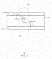
- the distance between the center point between each pair of signal lines 112, 114 may be referred to herein as "center-to-center displacement.”
- the center-to-center displacement is indicated by the arrows 302, 303, wherein the dashed line 306 is the centerline extending lengthwise between the signal pairs of the first signal line pair 112.
- the second signal line pair 114 includes a first segment, indicated by the dashed rectangle 310.
- the second signal line pair 114 includes a second segment indicated by the dashed rectangles 312.
- the second signal line pair 114 includes a third segment 314 indicated by the dashed rectangles 314.
- the third segment 314 couples the first segment 310 to the second segment 312.
- the first segment 310 runs lengthwise parallel to the first signal line pair 112.
- the second segment 312 runs lengthwise parallel to the first signal line pair.
- the second segment 312 is displaced from the centerline 306 in a direction that is opposite than the direction of displacement of the first segment 310. Therefore, the second signal line pair 114 receives crosstalk having a first polarity at the first segment 310, and crosstalk having a second polarity that is opposite to the first polarity, at the second segment 312.
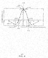
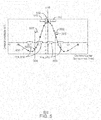
- the combination of the crosstalk having the first polarity with the crosstalk having the second opposite polarity results in a substantial cancellation of the crosstalk. It is appreciated that the crosstalk may be received at the first signal line pair 112 from the second signal line pair 114, and the crosstalk reduction may occur.
- the center point of the first segment 310 is indicated by the dashed line 504, and the center point of the second segment 312 is indicated by the dashed line 506. Even though the center points 504, 506 of the second signal line pair 114 are not at zero, the amplitude, indicated by the arrows 503, 505, of the crosstalk at each respective center point 504, 506 is equal in magnitude and of an opposite sign. The combination of crosstalk amplitude that is equal but of an opposite sign may reduce or cancel out the crosstalk between the first signal pair 112 and the second signal pair 114.
- Fig. 6 is a flow diagram illustrating a method of forming signal lines to reduce crosstalk.
- a pair of signal lines is formed at a first depth within a section of the circuit board.
- the pair of signal lines may be configured for differential signaling.
- crosstalk received at the first segment may be a first polarity and the crosstalk received at the second segment may be of a second polarity opposite of the first polarity.
- the crosstalk received at each of these segments may be significantly reduced.
- the first and second signal lines are both a differential pair of signal lines.
- the forming at blocks 602, 604, 606 may include forming a differential pair of signal lines for each of the first and second signal lines.
- the centerline may be a first centerline
- the second signal line comprises a second center line that extends lengthwise between the pair of signal lines of the second signal line.
- the first and second displacements may be from the first centerline to the second centerline.
- one of the signal lines is a differential pair and the other signal line is a unidirectional single-ended signal line.
- the forming of the signal lines at blocks 602, 604, 606, may include forming a differential pair and a unidirectional single-ended signal line. The first and second displacements are from the centerline of the differential pair to a centerline of the unidirectional single-ended signal line.
- a method of forming signal lines in a circuit board includes forming a pair of signal lines at a first depth of the circuit board, wherein a center line extends lengthwise between the pair of signal lines.
- the method includes forming a third signal line at a second depth of the circuit board, the third signal line comprising a segment that runs parallel to the pair of signal lines at a displacement distance from the center line.
- a machine-readable medium may include any mechanism for storing or transmitting information in a form readable by a machine, e.g., a computer.
- a machine-readable medium may include read only memory (ROM); random access memory (RAM); magnetic disk storage media; optical storage media; flash memory devices; or electrical, optical, acoustical or other form of propagated signals, e.g., carrier waves, infrared signals, digital signals, or the interfaces that transmit and/or receive signals, among others.
- An embodiment is an implementation or example.
- Reference in the specification to "an embodiment,” “one embodiment,” “some embodiments,” “various embodiments,” or “other embodiments” means that a particular feature, structure, or characteristic described in connection with the embodiments is included in at least some embodiments, but not necessarily all embodiments, of the present techniques.
- the various appearances of "an embodiment,” “one embodiment,” or “some embodiments” are not necessarily all referring to the same embodiments.
- the elements in some cases may each have a same reference number or a different reference number to suggest that the elements represented could be different and/or similar.
- an element may be flexible enough to have different implementations and work with some or all of the systems shown or described herein.
- the various elements shown in the figures may be the same or different. Which one is referred to as a first element and which is called a second element is arbitrary.
Landscapes
- Engineering & Computer Science (AREA)
- Microelectronics & Electronic Packaging (AREA)
- Physics & Mathematics (AREA)
- Electromagnetism (AREA)
- Manufacturing & Machinery (AREA)
- Structure Of Printed Boards (AREA)
- Details Of Connecting Devices For Male And Female Coupling (AREA)
- Cable Transmission Systems, Equalization Of Radio And Reduction Of Echo (AREA)
Applications Claiming Priority (1)
| Application Number | Priority Date | Filing Date | Title |
|---|---|---|---|
| US13/844,761 US9131603B2 (en) | 2013-03-15 | 2013-03-15 | Signal line pairs on a circuit board which are displaced from each other relative to a center line |
Publications (3)
| Publication Number | Publication Date |
|---|---|
| EP2779809A2 true EP2779809A2 (de) | 2014-09-17 |
| EP2779809A3 EP2779809A3 (de) | 2015-04-22 |
| EP2779809B1 EP2779809B1 (de) | 2018-12-05 |
Family
ID=50280235
Family Applications (1)
| Application Number | Title | Priority Date | Filing Date |
|---|---|---|---|
| EP14160014.8A Active EP2779809B1 (de) | 2013-03-15 | 2014-03-14 | Verlegung von zwei streifenleitungen zur verminderung des übersprechens |
Country Status (3)
| Country | Link |
|---|---|
| US (1) | US9131603B2 (de) |
| EP (1) | EP2779809B1 (de) |
| CN (1) | CN104053298B (de) |
Families Citing this family (8)
| Publication number | Priority date | Publication date | Assignee | Title |
|---|---|---|---|---|
| US9450557B2 (en) * | 2013-12-20 | 2016-09-20 | Nokia Technologies Oy | Programmable phase shifter with tunable capacitor bank network |
| CN105188266A (zh) * | 2015-08-27 | 2015-12-23 | 浪潮电子信息产业股份有限公司 | 一种dual模式高速信号线立体布线的方法 |
| US10798821B2 (en) | 2016-04-02 | 2020-10-06 | Intel Corporation | Circuit board having a passive device inside a via |
| KR102659671B1 (ko) * | 2016-11-01 | 2024-04-22 | 삼성전자주식회사 | 크로스토크 노이즈의 감소를 위한 신호 전송 채널, 이를 포함하는 모듈 기판 및 메모리 모듈 |
| CN110398681B (zh) * | 2019-07-26 | 2021-08-31 | 苏州浪潮智能科技有限公司 | 一种双带线检查方法及相关装置 |
| US12113265B2 (en) | 2021-03-26 | 2024-10-08 | Intel Corporation | Dual-stripline with crosstalk cancellation |
| KR20230030720A (ko) | 2021-08-25 | 2023-03-07 | 삼성전자주식회사 | 인쇄 회로 기판 및 이를 포함하는 메모리 모듈 |
| JP7844594B1 (ja) * | 2024-11-15 | 2026-04-13 | キヤノン株式会社 | 通信システム |
Family Cites Families (7)
| Publication number | Priority date | Publication date | Assignee | Title |
|---|---|---|---|---|
| US6058256A (en) | 1996-09-26 | 2000-05-02 | Lucent Technologies Inc. | Technique for effectively routing conduction paths in circuit layouts |
| US6300846B1 (en) | 1999-03-18 | 2001-10-09 | Molex Incorporated | Flat flexible cable with ground conductors |
| US6614325B1 (en) * | 2000-08-31 | 2003-09-02 | Northrop Grumman Corporation | RF/IF signal distribution network utilizing broadside coupled stripline |
| JP2002111324A (ja) * | 2000-09-28 | 2002-04-12 | Toshiba Corp | 信号伝送用回路基板、その製造方法及びそれを用いた電子機器 |
| US6573801B1 (en) | 2000-11-15 | 2003-06-03 | Intel Corporation | Electromagnetic coupler |
| JP4206045B2 (ja) * | 2004-01-28 | 2009-01-07 | 株式会社ワイケーシー | 差動信号用帯域通過フィルター及びこれを複数備える多周波アンテナ |
| CN101547552B (zh) * | 2008-03-28 | 2011-07-27 | 鸿富锦精密工业(深圳)有限公司 | 印刷电路板 |
-
2013
- 2013-03-15 US US13/844,761 patent/US9131603B2/en not_active Expired - Fee Related
-
2014
- 2014-03-14 EP EP14160014.8A patent/EP2779809B1/de active Active
- 2014-03-17 CN CN201410099286.3A patent/CN104053298B/zh active Active
Also Published As
| Publication number | Publication date |
|---|---|
| EP2779809B1 (de) | 2018-12-05 |
| US20140266490A1 (en) | 2014-09-18 |
| CN104053298A (zh) | 2014-09-17 |
| CN104053298B (zh) | 2018-02-23 |
| EP2779809A3 (de) | 2015-04-22 |
| US9131603B2 (en) | 2015-09-08 |
Similar Documents
| Publication | Publication Date | Title |
|---|---|---|
| EP2779809A2 (de) | Verlegung von zwei Streifenleitungen zur Verminderung des Übersprechens | |
| US8624687B2 (en) | Differential signal crosstalk reduction | |
| US9433081B1 (en) | Differential signal crosstalk minimization for dual stripline | |
| CN205584615U (zh) | 信号传输元器件及电子设备 | |
| US10897813B2 (en) | Differential trace pair system | |
| CN101562939A (zh) | 软性电路板 | |
| CN101594732A (zh) | 电路板 | |
| CN101861051A (zh) | 软性电路板 | |
| US9907160B2 (en) | Printed circuit board including differential transmission lines thereon and having a conductive structure which provides immunity to common-mode noise | |
| CN101394707B (zh) | 软性电路板 | |
| CN103270645B (zh) | 微带布线的串扰降低 | |
| CN104244580A (zh) | 软性电路板的差模信号传输线抗衰减接地结构 | |
| US9504159B2 (en) | Circuit component bridge device | |
| US20100207700A1 (en) | Micro-strip transmission line structure of a serpentine type | |
| US9379424B2 (en) | Compensation for length differences in vias associated with differential signaling | |
| US10014565B2 (en) | Signal transmission path comprised of first and second plurality of signal lines laminated with an interval regulation member | |
| US9337521B2 (en) | Crosstalk reduction in signal lines by crosstalk introduction | |
| US20240397612A1 (en) | Printed Circuit Board and Signal Transmission System | |
| US20150296609A1 (en) | Multi-circuit-layer circuit board | |
| WO2014109010A1 (ja) | ストレージ装置及び基板 | |
| US9113555B2 (en) | Apparatus for differential far-end crosstalk reduction | |
| CN104619112A (zh) | 多电路层电路板 | |
| WO2015192635A1 (zh) | 背板及具有该背板的通讯设备 | |
| KR102364151B1 (ko) | 연성회로기판 | |
| US20110205715A1 (en) | Transmission line circuit having pairs of crossing conductive lines |
Legal Events
| Date | Code | Title | Description |
|---|---|---|---|
| 17P | Request for examination filed |
Effective date: 20140314 |
|
| AK | Designated contracting states |
Kind code of ref document: A2 Designated state(s): AL AT BE BG CH CY CZ DE DK EE ES FI FR GB GR HR HU IE IS IT LI LT LU LV MC MK MT NL NO PL PT RO RS SE SI SK SM TR |
|
| AX | Request for extension of the european patent |
Extension state: BA ME |
|
| PUAI | Public reference made under article 153(3) epc to a published international application that has entered the european phase |
Free format text: ORIGINAL CODE: 0009012 |
|
| PUAL | Search report despatched |
Free format text: ORIGINAL CODE: 0009013 |
|
| AK | Designated contracting states |
Kind code of ref document: A3 Designated state(s): AL AT BE BG CH CY CZ DE DK EE ES FI FR GB GR HR HU IE IS IT LI LT LU LV MC MK MT NL NO PL PT RO RS SE SI SK SM TR |
|
| AX | Request for extension of the european patent |
Extension state: BA ME |
|
| RIC1 | Information provided on ipc code assigned before grant |
Ipc: H01P 3/08 20060101ALI20150313BHEP Ipc: H01P 11/00 20060101ALI20150313BHEP Ipc: H05K 1/02 20060101AFI20150313BHEP |
|
| GRAP | Despatch of communication of intention to grant a patent |
Free format text: ORIGINAL CODE: EPIDOSNIGR1 |
|
| STAA | Information on the status of an ep patent application or granted ep patent |
Free format text: STATUS: GRANT OF PATENT IS INTENDED |
|
| RIC1 | Information provided on ipc code assigned before grant |
Ipc: H05K 1/02 20060101AFI20180430BHEP Ipc: H01P 11/00 20060101ALI20180430BHEP Ipc: H01P 3/08 20060101ALI20180430BHEP |
|
| INTG | Intention to grant announced |
Effective date: 20180525 |
|
| GRAJ | Information related to disapproval of communication of intention to grant by the applicant or resumption of examination proceedings by the epo deleted |
Free format text: ORIGINAL CODE: EPIDOSDIGR1 |
|
| STAA | Information on the status of an ep patent application or granted ep patent |
Free format text: STATUS: REQUEST FOR EXAMINATION WAS MADE |
|
| GRAR | Information related to intention to grant a patent recorded |
Free format text: ORIGINAL CODE: EPIDOSNIGR71 |
|
| GRAS | Grant fee paid |
Free format text: ORIGINAL CODE: EPIDOSNIGR3 |
|
| STAA | Information on the status of an ep patent application or granted ep patent |
Free format text: STATUS: GRANT OF PATENT IS INTENDED |
|
| INTC | Intention to grant announced (deleted) | ||
| GRAA | (expected) grant |
Free format text: ORIGINAL CODE: 0009210 |
|
| STAA | Information on the status of an ep patent application or granted ep patent |
Free format text: STATUS: THE PATENT HAS BEEN GRANTED |
|
| AK | Designated contracting states |
Kind code of ref document: B1 Designated state(s): AL AT BE BG CH CY CZ DE DK EE ES FI FR GB GR HR HU IE IS IT LI LT LU LV MC MK MT NL NO PL PT RO RS SE SI SK SM TR |
|
| INTG | Intention to grant announced |
Effective date: 20181029 |
|
| REG | Reference to a national code |
Ref country code: GB Ref legal event code: FG4D |
|
| REG | Reference to a national code |
Ref country code: CH Ref legal event code: EP |
|
| REG | Reference to a national code |
Ref country code: AT Ref legal event code: REF Ref document number: 1074744 Country of ref document: AT Kind code of ref document: T Effective date: 20181215 |
|
| REG | Reference to a national code |
Ref country code: IE Ref legal event code: FG4D |
|
| REG | Reference to a national code |
Ref country code: DE Ref legal event code: R096 Ref document number: 602014037274 Country of ref document: DE |
|
| REG | Reference to a national code |
Ref country code: NL Ref legal event code: FP |
|
| REG | Reference to a national code |
Ref country code: AT Ref legal event code: MK05 Ref document number: 1074744 Country of ref document: AT Kind code of ref document: T Effective date: 20181205 |
|
| REG | Reference to a national code |
Ref country code: LT Ref legal event code: MG4D |
|
| PG25 | Lapsed in a contracting state [announced via postgrant information from national office to epo] |
Ref country code: ES Free format text: LAPSE BECAUSE OF FAILURE TO SUBMIT A TRANSLATION OF THE DESCRIPTION OR TO PAY THE FEE WITHIN THE PRESCRIBED TIME-LIMIT Effective date: 20181205 Ref country code: BG Free format text: LAPSE BECAUSE OF FAILURE TO SUBMIT A TRANSLATION OF THE DESCRIPTION OR TO PAY THE FEE WITHIN THE PRESCRIBED TIME-LIMIT Effective date: 20190305 Ref country code: LT Free format text: LAPSE BECAUSE OF FAILURE TO SUBMIT A TRANSLATION OF THE DESCRIPTION OR TO PAY THE FEE WITHIN THE PRESCRIBED TIME-LIMIT Effective date: 20181205 Ref country code: HR Free format text: LAPSE BECAUSE OF FAILURE TO SUBMIT A TRANSLATION OF THE DESCRIPTION OR TO PAY THE FEE WITHIN THE PRESCRIBED TIME-LIMIT Effective date: 20181205 Ref country code: AT Free format text: LAPSE BECAUSE OF FAILURE TO SUBMIT A TRANSLATION OF THE DESCRIPTION OR TO PAY THE FEE WITHIN THE PRESCRIBED TIME-LIMIT Effective date: 20181205 Ref country code: LV Free format text: LAPSE BECAUSE OF FAILURE TO SUBMIT A TRANSLATION OF THE DESCRIPTION OR TO PAY THE FEE WITHIN THE PRESCRIBED TIME-LIMIT Effective date: 20181205 Ref country code: NO Free format text: LAPSE BECAUSE OF FAILURE TO SUBMIT A TRANSLATION OF THE DESCRIPTION OR TO PAY THE FEE WITHIN THE PRESCRIBED TIME-LIMIT Effective date: 20190305 Ref country code: FI Free format text: LAPSE BECAUSE OF FAILURE TO SUBMIT A TRANSLATION OF THE DESCRIPTION OR TO PAY THE FEE WITHIN THE PRESCRIBED TIME-LIMIT Effective date: 20181205 |
|
| PG25 | Lapsed in a contracting state [announced via postgrant information from national office to epo] |
Ref country code: AL Free format text: LAPSE BECAUSE OF FAILURE TO SUBMIT A TRANSLATION OF THE DESCRIPTION OR TO PAY THE FEE WITHIN THE PRESCRIBED TIME-LIMIT Effective date: 20181205 Ref country code: SE Free format text: LAPSE BECAUSE OF FAILURE TO SUBMIT A TRANSLATION OF THE DESCRIPTION OR TO PAY THE FEE WITHIN THE PRESCRIBED TIME-LIMIT Effective date: 20181205 Ref country code: RS Free format text: LAPSE BECAUSE OF FAILURE TO SUBMIT A TRANSLATION OF THE DESCRIPTION OR TO PAY THE FEE WITHIN THE PRESCRIBED TIME-LIMIT Effective date: 20181205 Ref country code: GR Free format text: LAPSE BECAUSE OF FAILURE TO SUBMIT A TRANSLATION OF THE DESCRIPTION OR TO PAY THE FEE WITHIN THE PRESCRIBED TIME-LIMIT Effective date: 20190306 |
|
| PG25 | Lapsed in a contracting state [announced via postgrant information from national office to epo] |
Ref country code: PT Free format text: LAPSE BECAUSE OF FAILURE TO SUBMIT A TRANSLATION OF THE DESCRIPTION OR TO PAY THE FEE WITHIN THE PRESCRIBED TIME-LIMIT Effective date: 20190405 Ref country code: CZ Free format text: LAPSE BECAUSE OF FAILURE TO SUBMIT A TRANSLATION OF THE DESCRIPTION OR TO PAY THE FEE WITHIN THE PRESCRIBED TIME-LIMIT Effective date: 20181205 Ref country code: IT Free format text: LAPSE BECAUSE OF FAILURE TO SUBMIT A TRANSLATION OF THE DESCRIPTION OR TO PAY THE FEE WITHIN THE PRESCRIBED TIME-LIMIT Effective date: 20181205 Ref country code: PL Free format text: LAPSE BECAUSE OF FAILURE TO SUBMIT A TRANSLATION OF THE DESCRIPTION OR TO PAY THE FEE WITHIN THE PRESCRIBED TIME-LIMIT Effective date: 20181205 |
|
| PG25 | Lapsed in a contracting state [announced via postgrant information from national office to epo] |
Ref country code: SM Free format text: LAPSE BECAUSE OF FAILURE TO SUBMIT A TRANSLATION OF THE DESCRIPTION OR TO PAY THE FEE WITHIN THE PRESCRIBED TIME-LIMIT Effective date: 20181205 Ref country code: EE Free format text: LAPSE BECAUSE OF FAILURE TO SUBMIT A TRANSLATION OF THE DESCRIPTION OR TO PAY THE FEE WITHIN THE PRESCRIBED TIME-LIMIT Effective date: 20181205 Ref country code: IS Free format text: LAPSE BECAUSE OF FAILURE TO SUBMIT A TRANSLATION OF THE DESCRIPTION OR TO PAY THE FEE WITHIN THE PRESCRIBED TIME-LIMIT Effective date: 20190405 Ref country code: SK Free format text: LAPSE BECAUSE OF FAILURE TO SUBMIT A TRANSLATION OF THE DESCRIPTION OR TO PAY THE FEE WITHIN THE PRESCRIBED TIME-LIMIT Effective date: 20181205 Ref country code: RO Free format text: LAPSE BECAUSE OF FAILURE TO SUBMIT A TRANSLATION OF THE DESCRIPTION OR TO PAY THE FEE WITHIN THE PRESCRIBED TIME-LIMIT Effective date: 20181205 |
|
| REG | Reference to a national code |
Ref country code: DE Ref legal event code: R097 Ref document number: 602014037274 Country of ref document: DE |
|
| PLBE | No opposition filed within time limit |
Free format text: ORIGINAL CODE: 0009261 |
|
| STAA | Information on the status of an ep patent application or granted ep patent |
Free format text: STATUS: NO OPPOSITION FILED WITHIN TIME LIMIT |
|
| PG25 | Lapsed in a contracting state [announced via postgrant information from national office to epo] |
Ref country code: SI Free format text: LAPSE BECAUSE OF FAILURE TO SUBMIT A TRANSLATION OF THE DESCRIPTION OR TO PAY THE FEE WITHIN THE PRESCRIBED TIME-LIMIT Effective date: 20181205 Ref country code: DK Free format text: LAPSE BECAUSE OF FAILURE TO SUBMIT A TRANSLATION OF THE DESCRIPTION OR TO PAY THE FEE WITHIN THE PRESCRIBED TIME-LIMIT Effective date: 20181205 Ref country code: MC Free format text: LAPSE BECAUSE OF FAILURE TO SUBMIT A TRANSLATION OF THE DESCRIPTION OR TO PAY THE FEE WITHIN THE PRESCRIBED TIME-LIMIT Effective date: 20181205 |
|
| REG | Reference to a national code |
Ref country code: CH Ref legal event code: PL |
|
| 26N | No opposition filed |
Effective date: 20190906 |
|
| PG25 | Lapsed in a contracting state [announced via postgrant information from national office to epo] |
Ref country code: LU Free format text: LAPSE BECAUSE OF NON-PAYMENT OF DUE FEES Effective date: 20190314 |
|
| REG | Reference to a national code |
Ref country code: BE Ref legal event code: MM Effective date: 20190331 |
|
| PG25 | Lapsed in a contracting state [announced via postgrant information from national office to epo] |
Ref country code: LI Free format text: LAPSE BECAUSE OF NON-PAYMENT OF DUE FEES Effective date: 20190331 Ref country code: IE Free format text: LAPSE BECAUSE OF NON-PAYMENT OF DUE FEES Effective date: 20190314 Ref country code: CH Free format text: LAPSE BECAUSE OF NON-PAYMENT OF DUE FEES Effective date: 20190331 |
|
| PG25 | Lapsed in a contracting state [announced via postgrant information from national office to epo] |
Ref country code: BE Free format text: LAPSE BECAUSE OF NON-PAYMENT OF DUE FEES Effective date: 20190331 |
|
| PG25 | Lapsed in a contracting state [announced via postgrant information from national office to epo] |
Ref country code: TR Free format text: LAPSE BECAUSE OF FAILURE TO SUBMIT A TRANSLATION OF THE DESCRIPTION OR TO PAY THE FEE WITHIN THE PRESCRIBED TIME-LIMIT Effective date: 20181205 |
|
| PG25 | Lapsed in a contracting state [announced via postgrant information from national office to epo] |
Ref country code: MT Free format text: LAPSE BECAUSE OF NON-PAYMENT OF DUE FEES Effective date: 20190314 |
|
| PG25 | Lapsed in a contracting state [announced via postgrant information from national office to epo] |
Ref country code: CY Free format text: LAPSE BECAUSE OF FAILURE TO SUBMIT A TRANSLATION OF THE DESCRIPTION OR TO PAY THE FEE WITHIN THE PRESCRIBED TIME-LIMIT Effective date: 20181205 |
|
| PG25 | Lapsed in a contracting state [announced via postgrant information from national office to epo] |
Ref country code: HU Free format text: LAPSE BECAUSE OF FAILURE TO SUBMIT A TRANSLATION OF THE DESCRIPTION OR TO PAY THE FEE WITHIN THE PRESCRIBED TIME-LIMIT; INVALID AB INITIO Effective date: 20140314 |
|
| PG25 | Lapsed in a contracting state [announced via postgrant information from national office to epo] |
Ref country code: MK Free format text: LAPSE BECAUSE OF FAILURE TO SUBMIT A TRANSLATION OF THE DESCRIPTION OR TO PAY THE FEE WITHIN THE PRESCRIBED TIME-LIMIT Effective date: 20181205 |
|
| P01 | Opt-out of the competence of the unified patent court (upc) registered |
Effective date: 20230518 |
|
| PGFP | Annual fee paid to national office [announced via postgrant information from national office to epo] |
Ref country code: NL Payment date: 20260227 Year of fee payment: 13 |
|
| PGFP | Annual fee paid to national office [announced via postgrant information from national office to epo] |
Ref country code: GB Payment date: 20260223 Year of fee payment: 13 |
|
| PGFP | Annual fee paid to national office [announced via postgrant information from national office to epo] |
Ref country code: DE Payment date: 20260102 Year of fee payment: 13 |
|
| PGFP | Annual fee paid to national office [announced via postgrant information from national office to epo] |
Ref country code: FR Payment date: 20260223 Year of fee payment: 13 |