EP2779809B1 - Verlegung von zwei streifenleitungen zur verminderung des übersprechens - Google Patents
Verlegung von zwei streifenleitungen zur verminderung des übersprechens Download PDFInfo
- Publication number
- EP2779809B1 EP2779809B1 EP14160014.8A EP14160014A EP2779809B1 EP 2779809 B1 EP2779809 B1 EP 2779809B1 EP 14160014 A EP14160014 A EP 14160014A EP 2779809 B1 EP2779809 B1 EP 2779809B1
- Authority
- EP
- European Patent Office
- Prior art keywords
- pair
- segment
- signal
- signal lines
- line
- Prior art date
- Legal status (The legal status is an assumption and is not a legal conclusion. Google has not performed a legal analysis and makes no representation as to the accuracy of the status listed.)
- Active
Links
Images



Classifications
-
- H—ELECTRICITY
- H05—ELECTRIC TECHNIQUES NOT OTHERWISE PROVIDED FOR
- H05K—PRINTED CIRCUITS; CASINGS OR CONSTRUCTIONAL DETAILS OF ELECTRIC APPARATUS; MANUFACTURE OF ASSEMBLAGES OF ELECTRICAL COMPONENTS
- H05K1/00—Printed circuits
- H05K1/02—Details
- H05K1/0213—Electrical arrangements not otherwise provided for
- H05K1/0216—Reduction of cross-talk, noise or electromagnetic interference
- H05K1/0228—Compensation of cross-talk by a mutually correlated lay-out of printed circuit traces, e.g. for compensation of cross-talk in mounted connectors
-
- H—ELECTRICITY
- H01—ELECTRIC ELEMENTS
- H01P—WAVEGUIDES; RESONATORS, LINES, OR OTHER DEVICES OF THE WAVEGUIDE TYPE
- H01P11/00—Apparatus or processes specially adapted for manufacturing waveguides or resonators, lines, or other devices of the waveguide type
-
- H—ELECTRICITY
- H01—ELECTRIC ELEMENTS
- H01P—WAVEGUIDES; RESONATORS, LINES, OR OTHER DEVICES OF THE WAVEGUIDE TYPE
- H01P3/00—Waveguides; Transmission lines of the waveguide type
- H01P3/02—Waveguides; Transmission lines of the waveguide type with two longitudinal conductors
- H01P3/08—Microstrips; Strip lines
-
- H—ELECTRICITY
- H05—ELECTRIC TECHNIQUES NOT OTHERWISE PROVIDED FOR
- H05K—PRINTED CIRCUITS; CASINGS OR CONSTRUCTIONAL DETAILS OF ELECTRIC APPARATUS; MANUFACTURE OF ASSEMBLAGES OF ELECTRICAL COMPONENTS
- H05K1/00—Printed circuits
- H05K1/02—Details
- H05K1/0213—Electrical arrangements not otherwise provided for
- H05K1/0237—High frequency adaptations
- H05K1/0245—Lay-out of balanced signal pairs, e.g. differential lines or twisted lines
-
- H—ELECTRICITY
- H05—ELECTRIC TECHNIQUES NOT OTHERWISE PROVIDED FOR
- H05K—PRINTED CIRCUITS; CASINGS OR CONSTRUCTIONAL DETAILS OF ELECTRIC APPARATUS; MANUFACTURE OF ASSEMBLAGES OF ELECTRICAL COMPONENTS
- H05K1/00—Printed circuits
- H05K1/02—Details
- H05K1/0296—Conductive pattern lay-out details not covered by sub groups H05K1/02 - H05K1/0295
- H05K1/0298—Multilayer circuits
-
- H—ELECTRICITY
- H05—ELECTRIC TECHNIQUES NOT OTHERWISE PROVIDED FOR
- H05K—PRINTED CIRCUITS; CASINGS OR CONSTRUCTIONAL DETAILS OF ELECTRIC APPARATUS; MANUFACTURE OF ASSEMBLAGES OF ELECTRICAL COMPONENTS
- H05K2201/00—Indexing scheme relating to printed circuits covered by H05K1/00
- H05K2201/09—Shape and layout
- H05K2201/09209—Shape and layout details of conductors
- H05K2201/09218—Conductive traces
- H05K2201/09236—Parallel layout
-
- H—ELECTRICITY
- H05—ELECTRIC TECHNIQUES NOT OTHERWISE PROVIDED FOR
- H05K—PRINTED CIRCUITS; CASINGS OR CONSTRUCTIONAL DETAILS OF ELECTRIC APPARATUS; MANUFACTURE OF ASSEMBLAGES OF ELECTRICAL COMPONENTS
- H05K2201/00—Indexing scheme relating to printed circuits covered by H05K1/00
- H05K2201/09—Shape and layout
- H05K2201/09209—Shape and layout details of conductors
- H05K2201/09654—Shape and layout details of conductors covering at least two types of conductors provided for in H05K2201/09218 - H05K2201/095
- H05K2201/09709—Staggered pads, lands or terminals; Parallel conductors in different planes
-
- Y—GENERAL TAGGING OF NEW TECHNOLOGICAL DEVELOPMENTS; GENERAL TAGGING OF CROSS-SECTIONAL TECHNOLOGIES SPANNING OVER SEVERAL SECTIONS OF THE IPC; TECHNICAL SUBJECTS COVERED BY FORMER USPC CROSS-REFERENCE ART COLLECTIONS [XRACs] AND DIGESTS
- Y10—TECHNICAL SUBJECTS COVERED BY FORMER USPC
- Y10T—TECHNICAL SUBJECTS COVERED BY FORMER US CLASSIFICATION
- Y10T29/00—Metal working
- Y10T29/49—Method of mechanical manufacture
- Y10T29/49002—Electrical device making
- Y10T29/49117—Conductor or circuit manufacturing
- Y10T29/49124—On flat or curved insulated base, e.g., printed circuit, etc.
- Y10T29/49155—Manufacturing circuit on or in base
Definitions
- This disclosure relates generally to techniques for reducing crosstalk between signal lines in a computing device. More specifically, the disclosure describes a technique for routing transmission lines such that crosstalk between the lines is reduced.
- Circuit boards of a computing device may include traces configured to carry signals from one component of a circuit board to another.
- a stripline refers to a conductive trace that is located between two planar conductive structures with a dielectric material completely surrounding the trace. As a result, stripline traces are routed internal to the board and are not exposed to the external environment.
- a dual stripline refers to two traces located between planar conductive structures with a dielectric material surrounding both traces.
- Dual-stripline designs are used in stacked circuit boards and are popular in computer systems, such as half-width server platforms, because they save circuit board cost by lowering the number of sections in the stack due to a higher density of signaling.
- Adjacent traces of a dual-stripline design are co-located in the same section, and generate crosstalk between the two traces. Crosstalk tends to reduce circuit board performance, which tends to limit the data rate at which circuit boards can successfully operate.
- US 6 658 256 A discloses a routing system where a router interconnects circuit components with conduction paths, and a crosstalk analyzer is employed to audit the electrical crosstalk incurred in coupled path segments during the interconnection.
- the resulting crosstalk measures are compared with one or more acceptable crosstalk limits. If the measures exceed any limits, the unsatisfactory condition is fed back to the router, along with information on suggested re-arrangements of the segments. In response to this feedback, the router modifies the routed interconnections to reduce the crosstalk level.
- the subject matter disclosed herein relates to signal lines configured to reduce crosstalk. More specifically, the subject matter disclosed herein relates to a dual-stripline routing wherein one signal line crosses over the other signal line enabling a reduction of crosstalk.
- the techniques disclosed herein provide significant increases in routing density of circuit boards by arranging signal lines disposed between two planes in a way that reduces crosstalk between the signal lines. Increasing the routing density enables stacked circuit boards to be manufactured having a relatively smaller amount of stacked sections.
- Coupled may mean that two or more elements are in direct physical or electrical contact. However, “coupled” may also mean that two or more elements are not in direct contact with each other, but yet still co-operate or interact with each other.
- Fig. 1 is a block diagram illustrating a lengthwise side view of a stacked circuit board.
- the stacked circuit board 100 includes a first section indicated by the bracket 102, and a second section indicated by the bracket 104.
- the first section 102 and the second section 104 are separated by a conductive plane 106.
- the first section 102 includes a conductive plane 108.
- the second section 104 includes a conductive plane 110.
- the conductive planes 106, 108, 110 are reference planes such as ground planes.
- the conductive planes 106, 108, 110 are reference planes to signal lines, such as the signal lines 112, 114, 116, 118.
- the signal lines 112, 114, 116, 118 are configured to communicate signals across the circuit board 100.
- the signal lines 112, 114, 116, 118 may be disposed in a dielectric material 120.
- the signal lines 112, 114, 116, 118 may be configured to enable communication between the first section 102 and the second section 104 through vias (not shown).
- the signal lines 112 may cross over the signal lines 114 in the horizontal plane.
- the signal lines 112 can include a first segment that is disposed on a first side relative to a centerline of the signal line 114 and a second segment that is disposed on a second side relative to the centerline of the signal line 114. The disposition of the signal lines is described in more detail below.
- Fig. 2 is a block diagram illustrating an edge view of one section of the circuit board.
- the section may be the first section 102 of the circuit board 100 of Fig. 1 , including the signal lines 112, 114 within the dielectric material 120, and sandwiched by the conductive planes 106, 108.
- the conductive planes 106, 108 are ground planes and may provide a reference to the signal lines 112, 114.
- the signal lines 112, 114 may each include a pair of signal lines.
- each of the signal lines 112, 114 is configured to communicate differential signals wherein one of the signal lines in each pair is configured to carry a signal having a positive polarity and the other signal line in each pair is configured to carry a signal having a negative polarity.
- the signal lines 112, 114 may be disposed at a depth within the dielectric material with respect to a respective ground plane 106, 108.
- the pair of signal lines 112 may be disposed at a depth of H 1a with respect to the ground plane 108.
- the pair of signal lines 114 may be disposed at a depth of H 1b with respect to the ground plane 106.
- Each pair of signal lines 112, 114 may be disposed at a depth with respect to each other, as indicated by H 2 of Fig.
- Each pair of signal lines 112, 114 may have a center point between the pair.
- the signal pair 114 may have a center point coinciding with the dashed line 202 between the signal pair 114.
- the signal pair 112 may have a center point coinciding with the dashed line 204 between the signal pair 112.
- the distance between the center points may be the distance "D," indicated in Fig. 2 , between the dashed line 202 and the dashed line 204.
- the distance D between the center points may be referred to herein as "center-to-center displacement.”
- the center-to-center displacement is configured to enable crosstalk reduction between the pair of signal lines 112 and 114.
- the signal lines 112 and the signal lines 114 may be displaced with respect to each other's center lines 202, 204, respectively.
- the reduction as illustrated in Fig. 4 , enables crosstalk reduction by displacing the signal lines 112, 114 laterally away from each other to reduce, and in some cases cancel, crosstalk between the signal lines 112 and 114.
- Further embodiments such as the embodiment discussed in Fig. 3 , describe a first segment and a second segment on either side of a centerline of the signal line pair 114.
- Fig. 3 is a diagram illustrating a top view 300 of two signal line pairs.
- the signal line pairs may be the signal line pair 112 and the signal line pair 114 of Fig. 1 and Fig. 2 .
- the top view 300 of the signal line pairs 112, 114 is shown without the ground planes 106, 108, and without the dielectric material 120 shown in Figs. 1 and 2 .
- the top view 300 of the signal lines 112, 114 of Fig. 3 illustrates the geometry of the signal line pairs 112, 114 as they extend lengthwise through the circuit board section, such as the section 102 of Fig. 1 .
- the distance between the center point between each pair of signal lines 112, 114 may be referred to herein as "center-to-center displacement.”
- the center-to-center displacement is indicated by the arrows 302, 303, wherein the dashed line 306 is the centerline extending lengthwise between the signal pairs of the first signal line pair 112.
- the second signal line pair 114 includes a first segment, indicated by the dashed rectangle 310.
- the second signal line pair 114 includes a second segment indicated by the dashed rectangles 312.
- the second signal line pair 114 includes a third segment 314 indicated by the dashed rectangles 314.
- the third segment 314 couples the first segment 310 to the second segment 312.
- the dashed line 304 indicates the centerline extending lengthwise between the signal line pairs of the first segment 310 of the second signal line pair 114.
- the dashed line 308 indicates the centerline extending lengthwise between the signal line pairs of the second segment 312 of the second signal line pair 114.
- the arrow 302 illustrates the center-to-center displacement of the centerline 304 from the centerline 306.
- the arrow 303 illustrates the center-to-center displacement of the centerline 308 from the centerline 306.
- the first segment 310 runs lengthwise parallel to the first signal line pair 112.
- the second segment 312 runs lengthwise parallel to the first signal line pair.
- the second segment 312 is displaced from the centerline 306 in a direction that is opposite than the direction of displacement of the first segment 310. Therefore, the second signal line pair 114 receives crosstalk having a first polarity at the first segment 310, and crosstalk having a second polarity that is opposite to the first polarity, at the second segment 312.
- the combination of the crosstalk having the first polarity with the crosstalk having the second opposite polarity results in a substantial cancellation of the crosstalk. It is appreciated that the crosstalk may be received at the first signal line pair 112 from the second signal line pair 114, and the crosstalk reduction may occur.
- the displacement 302 may be referred to herein as a first displacement, and the displacement 303 may be referred herein as a second displacement.
- the second displacement 303 is the same displacement as the first displacement 302.
- the respective displacements are different, such as when the signal lines 112 and 114 are misaligned due to manufacturing tolerances discussed below in reference to Fig. 7.
- Fig. 3 illustrates two pairs of signal lines 112, 114
- one of the signal lines may be unidirectional single-ended signal as long as the other signal line is configured to be a pair differential signal lines.
- the geometry of the signal lines enables crosstalk reduction because the reduction depends, in part on opposing polarities being transmitted in at least one of the signal lines as differential pairs.
- Fig. 3 illustrates only three segments 310, 312, 314 of the second signal line pair 114
- additional segments are possible.
- the substantial similarity of the distances 316, 318 enable crosstalk amplitude to be substantially similar yet of opposite polarities. Therefore, additional segments of the second signal line pair 114 that traverse the first signal line pair 112 are contemplated as long as additional segments incorporate similar dimensions such as the relative distance 316 to the distance 318.
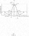
- Fig. 4 is a graph illustrating crosstalk amplitude as a measure of displacement spacing between the centerlines of the signal lines. As discussed above in reference to Figs. 2 and 3 , the spacing between the centerlines of the signal line pairs enables crosstalk to be reduced.
- the graph 400 illustrates the amplitude of crosstalk is zero at points 402, 404, and is at a peak amplitude at point 406.
- the graph of the line 408 shows the change in crosstalk amplitude and polarity as a function of distance from the peak amplitude 406.
- the peak amplitude 406 occurs at the center point indicated by the dashed line 410 between the first signal line pair 112.
- the center point 410 coincides with the center line 306 discussed above in relation to Fig. 3 .
- the center point of the first segment 310 of the second signal line pair 114 is indicated by the dashed line 412.
- the center point 412 coincides with the center line 304 discussed above in reference to Fig. 3 .
- the center point of the second segment 312 of the second signal pair 114 is indicated by the dashed line 414.
- the center point 414 coincides with the center line 308 discussed above in relation to Fig. 3 .
- the crosstalk amplitude decreases until it reaches zero, after which point, the amplitude of the crosstalk becomes a negative value.
- the center points 412, 414 of the second signal line pair 114 are disposed at a displacement coinciding with the zero points 402,404, the crosstalk between the first signal line pair 112 and the second signal line pair 114 is reduced.
- Fig. 5 is a graph illustrating crosstalk amplitude as a measure of spacing displacement between the centerlines of the signal lines when the signal lines are misaligned.
- the signal lines 112, 114 may be misaligned due to manufacturing tolerances.
- the center point 410 is the same center point as illustrated in Fig. 4 .
- the first and second segments 310, 312 of the second signal line pair 114 may reduce crosstalk by being disposed at a displacement from the center point 410 of the first signal line pair 114.
- the center points of the second signal line pair 114 have been shifted as indicated by the arrows 502.
- the center point of the first segment 310 is indicated by the dashed line 504, and the center point of the second segment 312 is indicated by the dashed line 506. Even though the center points 504, 506 of the second signal line pair 114 are not at zero, the amplitude, indicated by the arrows 503, 505, of the crosstalk at each respective center point 504, 506 is equal in magnitude and of an opposite sign. The combination of crosstalk amplitude that is equal but of an opposite sign may reduce or cancel out the crosstalk between the first signal pair 112 and the second signal pair 114.
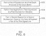
- Fig. 6 is a flow diagram illustrating a method of forming signal lines to reduce crosstalk.
- a pair of signal lines is formed at a first depth within a section of the circuit board.
- the pair of signal lines may be configured for differential signaling.
- a third signal line is formed at a second depth of the circuit board comprising a first segment at a first displacement distance.
- the first segment of the third signal line formed at block 604 runs parallel to the first signal line at a first displacement distance from the center line.
- a second segment of the third signal line is formed.
- the second segment runs parallel to the first signal line.
- the second segment runs on the other side, with respect to the first segment, of the center line.
- the first and second segment may be on opposite sides of the centerline of the pair of signal lines formed at block 602.
- crosstalk received at the first segment may be a first polarity and the crosstalk received at the second segment may be of a second polarity opposite of the first polarity.
- the crosstalk received at each of these segments may be significantly reduced.
- the method 800 may also include forming (not shown) a third segment of the third signal line.
- the third segment may couple the first segment and the second segment.
- the third segment is disposed at an angle relative to the first segment and to the second segment, respectively.
- the first and second signal lines are both a differential pair of signal lines.
- the forming at blocks 602, 604, 606 may include forming a differential pair of signal lines for each of the first and second signal lines.
- the centerline may be a first centerline
- the second signal line comprises a second center line that extends lengthwise between the pair of signal lines of the second signal line.
- the first and second displacements may be from the first centerline to the second centerline.
- one of the signal lines is a differential pair and the other signal line is a unidirectional single-ended signal line.
- the forming of the signal lines at blocks 602, 604, 606, may include forming a differential pair and a unidirectional single-ended signal line. The first and second displacements are from the centerline of the differential pair to a centerline of the unidirectional single-ended signal line.
- the method 800 may include forming a first reference plane, and forming a second reference plane.
- the signal lines may be formed between the reference planes within a dielectric. Therefore, the method 800 may include forming a dielectric disposed between the first reference place and the second reference place, wherein the first signal line and the second signal line are disposed within the dielectric.
- the method 800 may include forming a third segment of the second signal line.
- the third segment couples the first segment and the third segment.
- a circuit board according to the invention is defined in claim 1.
- the circuit board includes a pair of signal lines at a first depth of the circuit board, wherein a center line extends lengthwise between the pair of signal lines.
- the circuit board includes a third signal line at a second depth of the circuit board, the third signal line comprising a segment that runs parallel to the pair of signal lines at a displacement distance from the center line.
- a stripline signal system is defined in claim 6.
- the stripline signal system includes a pair of signal lines disposed within a dielectric, the pair of signal lines disposed at a first depth of the dielectric, wherein a center line extends lengthwise between the pair of signal lines.
- the stripline signal system includes a third signal line disposed within the dielectric, the third signal line comprising a segment running parallel to the pair of signal lines, the segment disposed at a displacement distance relative to the center line.
- a method of forming signal lines in a circuit board according to the invention is defined in claim 11.
- the method includes forming a pair of signal lines at a first depth of the circuit board, wherein a center line extends lengthwise between the pair of signal lines.
- the method includes forming a third signal line at a second depth of the circuit board, the third signal line comprising a segment that runs parallel to the pair of signal lines at a displacement distance from the center line.
- a machine-readable medium may include any mechanism for storing or transmitting information in a form readable by a machine, e.g., a computer.
- a machine-readable medium may include read only memory (ROM); random access memory (RAM); magnetic disk storage media; optical storage media; flash memory devices; or electrical, optical, acoustical or other form of propagated signals, e.g., carrier waves, infrared signals, digital signals, or the interfaces that transmit and/or receive signals, among others.
- the elements in some cases may each have a same reference number or a different reference number to suggest that the elements represented could be different and/or similar.
- an element may be flexible enough to have different implementations and work with some or all of the systems shown or described herein.
- the various elements shown in the figures may be the same or different. Which one is referred to as a first element and which is called a second element is arbitrary.
Landscapes
- Engineering & Computer Science (AREA)
- Microelectronics & Electronic Packaging (AREA)
- Physics & Mathematics (AREA)
- Electromagnetism (AREA)
- Manufacturing & Machinery (AREA)
- Structure Of Printed Boards (AREA)
- Details Of Connecting Devices For Male And Female Coupling (AREA)
- Cable Transmission Systems, Equalization Of Radio And Reduction Of Echo (AREA)
Claims (11)
- Leiterplatte (100), umfassend:ein Paar Differenzsignalleitungen (112) an einer ersten Tiefe der Leiterplatte, wobei sich eine Mittellinie (306) in Längsrichtung zwischen dem Signalleitungspaar erstreckt; undeine dritte Signalleitung an einer zweiten Tiefe der Leiterplatte, die dritte Signalleitung umfassend ein Segment, das parallel zu dem Signalleitungspaar in einem Verschiebungsabstand von der Mittellinie verläuft,wobei das Segment ein erstes Segment (310) ist und der Verschiebungsabstand eine erste Verschiebung (302) ist, wobei die dritte Signalleitung ein zweites Segment (312), das parallel zu dem Signalleitungspaar auf der anderen Seite der Mittellinie in einem zweiten Verschiebungsabstand (303) zu der Mittellinie verläuft, und ein drittes Segment (314), das das erste Segment (310) an das zweite Segment (312) koppelt, umfasst.
- Leiterplatte nach Anspruch 1, wobei das Signalleitungspaar und die dritte Signalleitung in der Leiterplatte angeordnet sind, umfassend:eine erste Referenzebene (106);eine zweite Referenzebene (108); undein Dielektrikum (120), das zwischen der ersten Referenzebene und der zweiten Referenzebene angeordnet ist, wobei das Signalleitungspaar und die dritte Signalleitung in dem Dielektrikum angeordnet sind.
- Leiterplatte nach Anspruch 1, umfassend eine vierte Signalleitung an der zweiten Tiefe, wobei die dritte Signalleitung und die vierte Signalleitung ein zweites Paar (114) von Signalleitungen zum Übermitteln von Differenzsignalen bilden.
- Leiterplatte nach Anspruch 3, wobei die Mittellinie des Signalleitungspaars eine erste Mittellinie (306) ist und wobei sich eine zweite Mittellinie (304; 308) in Längsrichtung zwischen dem zweiten Signalleitungspaar erstreckt und wobei die ersten und zweiten Verschiebungsabstände von der ersten Mittellinie des ersten Signalleitungspaars zu der zweiten Mittellinie des zweiten Signalleitungspaars sind.
- Leiterplatte nach Anspruch 1, wobei der erste Verschiebungsabstand und der zweite Verschiebungsabstand ungefähr gleich sind.
- Streifenleitungssignalsystem, umfassend eine Leiterplatte nach Anspruch 1, wobei:das Differenzsignalleitungspaar in einem Dielektrikum angeordnet ist, wobei das Dielektrikum ein Teil der Leiterplatte ist, wobei das Signalleitungspaar an einer ersten Tiefe des Dielektrikums angeordnet ist, wobei sich eine Mittellinie in Längsrichtung zwischen dem Signalleitungspaar erstreckt; unddie dritte Signalleitung in dem Dielektrikum angeordnet ist, die dritte Signalleitung umfassend ein Segment, das parallel zu dem Signalleitungspaar verläuft, wobei das Segment in einem Verschiebungsabstand bezogen auf die Mittellinie angeordnet ist, wobei das Segment ein erstes Segment ist und der Verschiebungsabstand eine erste Verschiebung ist, die dritte Signalleitung umfassend ein zweites Segment, das parallel zu dem Signalleitungspaar verläuft, wobei das zweite Segment in einem zweiten Verschiebungsabstand bezogen auf die Mittellinie in einer Richtung gegenüber der ersten Verschiebung angeordnet ist und ein drittes Segment das erste Segment an das zweite Segment koppelt.
- Streifenleitungssignalsystem nach Anspruch 6, wobei die Leiterplatte Folgendes umfasst:eine erste Referenzebene; undeine zweite Referenzebene, wobei das Dielektrikum zwischen der ersten Referenzebene und der zweiten Referenzebene angeordnet ist.
- Streifenleitungssignalsystem nach Anspruch 6, umfassend eine vierte Signalleitung an der zweiten Tiefe, wobei die dritte Signalleitung und die vierte Signalleitung ein zweites Paar von Signalleitungen zum Übermitteln von Differenzsignalen bilden.
- Streifenleitungssignalsystem nach Anspruch 8, wobei die Mittellinie der ersten Signalleitung eine erste Mittellinie ist und wobei sich eine zweite Mittellinie in Längsrichtung zwischen dem zweiten Signalleitungspaar erstreckt und wobei die ersten und zweiten Verschiebungsabstände von der ersten Mittellinie des ersten Signalleitungspaars zu der zweiten Mittellinie des zweiten Signalleitungspaars sind.
- Streifenleitungssignalsystem nach Anspruch 6, wobei der erste Verschiebungsabstand und der zweite Verschiebungsabstand ungefähr gleich sind.
- Verfahren zum Bilden von Signalleitungen in einer Leiterplatte, umfassend:Bilden eines Differenzsignalleitungspaars an einer ersten Tiefe der Leiterplatte (602), wobei sich eine Mittellinie in Längsrichtung zwischen dem Signalleitungspaar erstreckt; undBilden einer dritten Signalleitung an einer zweiten Tiefe der Leiterplatte, die dritte Signalleitung umfassend ein Segment, das parallel zu dem Signalleitungspaar in einem Verschiebungsabstand von der Mittellinie verläuft,wobei das Segment ein erstes Segment ist und der Verschiebungsabstand eine erste Verschiebung (604) ist, wobei das Bilden der dritten Signalleitung ein Bilden eines zweiten Segments, das parallel zu dem Signalleitungspaar auf der anderen Seite der Mittellinie in einem zweiten Verschiebungsabstand (606) verläuft, und ein Bilden eines dritten Segments, das das erste Segment an das zweite Segment koppelt, umfasst.
Applications Claiming Priority (1)
| Application Number | Priority Date | Filing Date | Title |
|---|---|---|---|
| US13/844,761 US9131603B2 (en) | 2013-03-15 | 2013-03-15 | Signal line pairs on a circuit board which are displaced from each other relative to a center line |
Publications (3)
| Publication Number | Publication Date |
|---|---|
| EP2779809A2 EP2779809A2 (de) | 2014-09-17 |
| EP2779809A3 EP2779809A3 (de) | 2015-04-22 |
| EP2779809B1 true EP2779809B1 (de) | 2018-12-05 |
Family
ID=50280235
Family Applications (1)
| Application Number | Title | Priority Date | Filing Date |
|---|---|---|---|
| EP14160014.8A Active EP2779809B1 (de) | 2013-03-15 | 2014-03-14 | Verlegung von zwei streifenleitungen zur verminderung des übersprechens |
Country Status (3)
| Country | Link |
|---|---|
| US (1) | US9131603B2 (de) |
| EP (1) | EP2779809B1 (de) |
| CN (1) | CN104053298B (de) |
Cited By (1)
| Publication number | Priority date | Publication date | Assignee | Title |
|---|---|---|---|---|
| CN110398681A (zh) * | 2019-07-26 | 2019-11-01 | 苏州浪潮智能科技有限公司 | 一种双带线检查方法及相关装置 |
Families Citing this family (7)
| Publication number | Priority date | Publication date | Assignee | Title |
|---|---|---|---|---|
| US9450557B2 (en) * | 2013-12-20 | 2016-09-20 | Nokia Technologies Oy | Programmable phase shifter with tunable capacitor bank network |
| CN105188266A (zh) * | 2015-08-27 | 2015-12-23 | 浪潮电子信息产业股份有限公司 | 一种dual模式高速信号线立体布线的方法 |
| US10798821B2 (en) | 2016-04-02 | 2020-10-06 | Intel Corporation | Circuit board having a passive device inside a via |
| KR102659671B1 (ko) * | 2016-11-01 | 2024-04-22 | 삼성전자주식회사 | 크로스토크 노이즈의 감소를 위한 신호 전송 채널, 이를 포함하는 모듈 기판 및 메모리 모듈 |
| US12113265B2 (en) | 2021-03-26 | 2024-10-08 | Intel Corporation | Dual-stripline with crosstalk cancellation |
| KR20230030720A (ko) | 2021-08-25 | 2023-03-07 | 삼성전자주식회사 | 인쇄 회로 기판 및 이를 포함하는 메모리 모듈 |
| JP7844594B1 (ja) * | 2024-11-15 | 2026-04-13 | キヤノン株式会社 | 通信システム |
Family Cites Families (7)
| Publication number | Priority date | Publication date | Assignee | Title |
|---|---|---|---|---|
| US6058256A (en) | 1996-09-26 | 2000-05-02 | Lucent Technologies Inc. | Technique for effectively routing conduction paths in circuit layouts |
| US6300846B1 (en) | 1999-03-18 | 2001-10-09 | Molex Incorporated | Flat flexible cable with ground conductors |
| US6614325B1 (en) * | 2000-08-31 | 2003-09-02 | Northrop Grumman Corporation | RF/IF signal distribution network utilizing broadside coupled stripline |
| JP2002111324A (ja) * | 2000-09-28 | 2002-04-12 | Toshiba Corp | 信号伝送用回路基板、その製造方法及びそれを用いた電子機器 |
| US6573801B1 (en) | 2000-11-15 | 2003-06-03 | Intel Corporation | Electromagnetic coupler |
| JP4206045B2 (ja) * | 2004-01-28 | 2009-01-07 | 株式会社ワイケーシー | 差動信号用帯域通過フィルター及びこれを複数備える多周波アンテナ |
| CN101547552B (zh) * | 2008-03-28 | 2011-07-27 | 鸿富锦精密工业(深圳)有限公司 | 印刷电路板 |
-
2013
- 2013-03-15 US US13/844,761 patent/US9131603B2/en not_active Expired - Fee Related
-
2014
- 2014-03-14 EP EP14160014.8A patent/EP2779809B1/de active Active
- 2014-03-17 CN CN201410099286.3A patent/CN104053298B/zh active Active
Non-Patent Citations (1)
| Title |
|---|
| None * |
Cited By (1)
| Publication number | Priority date | Publication date | Assignee | Title |
|---|---|---|---|---|
| CN110398681A (zh) * | 2019-07-26 | 2019-11-01 | 苏州浪潮智能科技有限公司 | 一种双带线检查方法及相关装置 |
Also Published As
| Publication number | Publication date |
|---|---|
| EP2779809A2 (de) | 2014-09-17 |
| US20140266490A1 (en) | 2014-09-18 |
| CN104053298A (zh) | 2014-09-17 |
| CN104053298B (zh) | 2018-02-23 |
| EP2779809A3 (de) | 2015-04-22 |
| US9131603B2 (en) | 2015-09-08 |
Similar Documents
| Publication | Publication Date | Title |
|---|---|---|
| EP2779809B1 (de) | Verlegung von zwei streifenleitungen zur verminderung des übersprechens | |
| US8624687B2 (en) | Differential signal crosstalk reduction | |
| US9433081B1 (en) | Differential signal crosstalk minimization for dual stripline | |
| US10897813B2 (en) | Differential trace pair system | |
| US20130278348A1 (en) | Crosstalk cancellation and/or reduction | |
| US20130077268A1 (en) | Circuit board with air hole | |
| US6710675B2 (en) | Transmission line parasitic element discontinuity cancellation | |
| US20200253036A1 (en) | High speed serial link intra pair skew correction | |
| CN101378618A (zh) | 印刷电路板 | |
| CN104244580A (zh) | 软性电路板的差模信号传输线抗衰减接地结构 | |
| US20170013716A1 (en) | Differential trace pair system | |
| US20180279465A1 (en) | Multilayer Wiring Board and Differential Transmission Module | |
| WO2009057856A1 (en) | A micro-strip transmission line structure of a serpentine type | |
| WO2012087647A1 (en) | Crosstalk reduction for microstrip routing | |
| US9504159B2 (en) | Circuit component bridge device | |
| US9379424B2 (en) | Compensation for length differences in vias associated with differential signaling | |
| JP2017183638A (ja) | 多層プリント配線板 | |
| KR100744535B1 (ko) | 누화 간섭을 감소시키는 가드 트레이스 패턴 및 상기 가드트레이스 패턴을 구비하는 인쇄회로기판 | |
| US9337521B2 (en) | Crosstalk reduction in signal lines by crosstalk introduction | |
| US20240397612A1 (en) | Printed Circuit Board and Signal Transmission System | |
| US20170064817A1 (en) | Printed circuit board | |
| US20150296609A1 (en) | Multi-circuit-layer circuit board | |
| WO2014109010A1 (ja) | ストレージ装置及び基板 | |
| US7070341B2 (en) | High-density fiber-optic module with multi-fold flexible circuit | |
| CN104619112A (zh) | 多电路层电路板 |
Legal Events
| Date | Code | Title | Description |
|---|---|---|---|
| 17P | Request for examination filed |
Effective date: 20140314 |
|
| AK | Designated contracting states |
Kind code of ref document: A2 Designated state(s): AL AT BE BG CH CY CZ DE DK EE ES FI FR GB GR HR HU IE IS IT LI LT LU LV MC MK MT NL NO PL PT RO RS SE SI SK SM TR |
|
| AX | Request for extension of the european patent |
Extension state: BA ME |
|
| PUAI | Public reference made under article 153(3) epc to a published international application that has entered the european phase |
Free format text: ORIGINAL CODE: 0009012 |
|
| PUAL | Search report despatched |
Free format text: ORIGINAL CODE: 0009013 |
|
| AK | Designated contracting states |
Kind code of ref document: A3 Designated state(s): AL AT BE BG CH CY CZ DE DK EE ES FI FR GB GR HR HU IE IS IT LI LT LU LV MC MK MT NL NO PL PT RO RS SE SI SK SM TR |
|
| AX | Request for extension of the european patent |
Extension state: BA ME |
|
| RIC1 | Information provided on ipc code assigned before grant |
Ipc: H01P 3/08 20060101ALI20150313BHEP Ipc: H01P 11/00 20060101ALI20150313BHEP Ipc: H05K 1/02 20060101AFI20150313BHEP |
|
| GRAP | Despatch of communication of intention to grant a patent |
Free format text: ORIGINAL CODE: EPIDOSNIGR1 |
|
| STAA | Information on the status of an ep patent application or granted ep patent |
Free format text: STATUS: GRANT OF PATENT IS INTENDED |
|
| RIC1 | Information provided on ipc code assigned before grant |
Ipc: H05K 1/02 20060101AFI20180430BHEP Ipc: H01P 11/00 20060101ALI20180430BHEP Ipc: H01P 3/08 20060101ALI20180430BHEP |
|
| INTG | Intention to grant announced |
Effective date: 20180525 |
|
| GRAJ | Information related to disapproval of communication of intention to grant by the applicant or resumption of examination proceedings by the epo deleted |
Free format text: ORIGINAL CODE: EPIDOSDIGR1 |
|
| STAA | Information on the status of an ep patent application or granted ep patent |
Free format text: STATUS: REQUEST FOR EXAMINATION WAS MADE |
|
| GRAR | Information related to intention to grant a patent recorded |
Free format text: ORIGINAL CODE: EPIDOSNIGR71 |
|
| GRAS | Grant fee paid |
Free format text: ORIGINAL CODE: EPIDOSNIGR3 |
|
| STAA | Information on the status of an ep patent application or granted ep patent |
Free format text: STATUS: GRANT OF PATENT IS INTENDED |
|
| INTC | Intention to grant announced (deleted) | ||
| GRAA | (expected) grant |
Free format text: ORIGINAL CODE: 0009210 |
|
| STAA | Information on the status of an ep patent application or granted ep patent |
Free format text: STATUS: THE PATENT HAS BEEN GRANTED |
|
| AK | Designated contracting states |
Kind code of ref document: B1 Designated state(s): AL AT BE BG CH CY CZ DE DK EE ES FI FR GB GR HR HU IE IS IT LI LT LU LV MC MK MT NL NO PL PT RO RS SE SI SK SM TR |
|
| INTG | Intention to grant announced |
Effective date: 20181029 |
|
| REG | Reference to a national code |
Ref country code: GB Ref legal event code: FG4D |
|
| REG | Reference to a national code |
Ref country code: CH Ref legal event code: EP |
|
| REG | Reference to a national code |
Ref country code: AT Ref legal event code: REF Ref document number: 1074744 Country of ref document: AT Kind code of ref document: T Effective date: 20181215 |
|
| REG | Reference to a national code |
Ref country code: IE Ref legal event code: FG4D |
|
| REG | Reference to a national code |
Ref country code: DE Ref legal event code: R096 Ref document number: 602014037274 Country of ref document: DE |
|
| REG | Reference to a national code |
Ref country code: NL Ref legal event code: FP |
|
| REG | Reference to a national code |
Ref country code: AT Ref legal event code: MK05 Ref document number: 1074744 Country of ref document: AT Kind code of ref document: T Effective date: 20181205 |
|
| REG | Reference to a national code |
Ref country code: LT Ref legal event code: MG4D |
|
| PG25 | Lapsed in a contracting state [announced via postgrant information from national office to epo] |
Ref country code: ES Free format text: LAPSE BECAUSE OF FAILURE TO SUBMIT A TRANSLATION OF THE DESCRIPTION OR TO PAY THE FEE WITHIN THE PRESCRIBED TIME-LIMIT Effective date: 20181205 Ref country code: BG Free format text: LAPSE BECAUSE OF FAILURE TO SUBMIT A TRANSLATION OF THE DESCRIPTION OR TO PAY THE FEE WITHIN THE PRESCRIBED TIME-LIMIT Effective date: 20190305 Ref country code: LT Free format text: LAPSE BECAUSE OF FAILURE TO SUBMIT A TRANSLATION OF THE DESCRIPTION OR TO PAY THE FEE WITHIN THE PRESCRIBED TIME-LIMIT Effective date: 20181205 Ref country code: HR Free format text: LAPSE BECAUSE OF FAILURE TO SUBMIT A TRANSLATION OF THE DESCRIPTION OR TO PAY THE FEE WITHIN THE PRESCRIBED TIME-LIMIT Effective date: 20181205 Ref country code: AT Free format text: LAPSE BECAUSE OF FAILURE TO SUBMIT A TRANSLATION OF THE DESCRIPTION OR TO PAY THE FEE WITHIN THE PRESCRIBED TIME-LIMIT Effective date: 20181205 Ref country code: LV Free format text: LAPSE BECAUSE OF FAILURE TO SUBMIT A TRANSLATION OF THE DESCRIPTION OR TO PAY THE FEE WITHIN THE PRESCRIBED TIME-LIMIT Effective date: 20181205 Ref country code: NO Free format text: LAPSE BECAUSE OF FAILURE TO SUBMIT A TRANSLATION OF THE DESCRIPTION OR TO PAY THE FEE WITHIN THE PRESCRIBED TIME-LIMIT Effective date: 20190305 Ref country code: FI Free format text: LAPSE BECAUSE OF FAILURE TO SUBMIT A TRANSLATION OF THE DESCRIPTION OR TO PAY THE FEE WITHIN THE PRESCRIBED TIME-LIMIT Effective date: 20181205 |
|
| PG25 | Lapsed in a contracting state [announced via postgrant information from national office to epo] |
Ref country code: AL Free format text: LAPSE BECAUSE OF FAILURE TO SUBMIT A TRANSLATION OF THE DESCRIPTION OR TO PAY THE FEE WITHIN THE PRESCRIBED TIME-LIMIT Effective date: 20181205 Ref country code: SE Free format text: LAPSE BECAUSE OF FAILURE TO SUBMIT A TRANSLATION OF THE DESCRIPTION OR TO PAY THE FEE WITHIN THE PRESCRIBED TIME-LIMIT Effective date: 20181205 Ref country code: RS Free format text: LAPSE BECAUSE OF FAILURE TO SUBMIT A TRANSLATION OF THE DESCRIPTION OR TO PAY THE FEE WITHIN THE PRESCRIBED TIME-LIMIT Effective date: 20181205 Ref country code: GR Free format text: LAPSE BECAUSE OF FAILURE TO SUBMIT A TRANSLATION OF THE DESCRIPTION OR TO PAY THE FEE WITHIN THE PRESCRIBED TIME-LIMIT Effective date: 20190306 |
|
| PG25 | Lapsed in a contracting state [announced via postgrant information from national office to epo] |
Ref country code: PT Free format text: LAPSE BECAUSE OF FAILURE TO SUBMIT A TRANSLATION OF THE DESCRIPTION OR TO PAY THE FEE WITHIN THE PRESCRIBED TIME-LIMIT Effective date: 20190405 Ref country code: CZ Free format text: LAPSE BECAUSE OF FAILURE TO SUBMIT A TRANSLATION OF THE DESCRIPTION OR TO PAY THE FEE WITHIN THE PRESCRIBED TIME-LIMIT Effective date: 20181205 Ref country code: IT Free format text: LAPSE BECAUSE OF FAILURE TO SUBMIT A TRANSLATION OF THE DESCRIPTION OR TO PAY THE FEE WITHIN THE PRESCRIBED TIME-LIMIT Effective date: 20181205 Ref country code: PL Free format text: LAPSE BECAUSE OF FAILURE TO SUBMIT A TRANSLATION OF THE DESCRIPTION OR TO PAY THE FEE WITHIN THE PRESCRIBED TIME-LIMIT Effective date: 20181205 |
|
| PG25 | Lapsed in a contracting state [announced via postgrant information from national office to epo] |
Ref country code: SM Free format text: LAPSE BECAUSE OF FAILURE TO SUBMIT A TRANSLATION OF THE DESCRIPTION OR TO PAY THE FEE WITHIN THE PRESCRIBED TIME-LIMIT Effective date: 20181205 Ref country code: EE Free format text: LAPSE BECAUSE OF FAILURE TO SUBMIT A TRANSLATION OF THE DESCRIPTION OR TO PAY THE FEE WITHIN THE PRESCRIBED TIME-LIMIT Effective date: 20181205 Ref country code: IS Free format text: LAPSE BECAUSE OF FAILURE TO SUBMIT A TRANSLATION OF THE DESCRIPTION OR TO PAY THE FEE WITHIN THE PRESCRIBED TIME-LIMIT Effective date: 20190405 Ref country code: SK Free format text: LAPSE BECAUSE OF FAILURE TO SUBMIT A TRANSLATION OF THE DESCRIPTION OR TO PAY THE FEE WITHIN THE PRESCRIBED TIME-LIMIT Effective date: 20181205 Ref country code: RO Free format text: LAPSE BECAUSE OF FAILURE TO SUBMIT A TRANSLATION OF THE DESCRIPTION OR TO PAY THE FEE WITHIN THE PRESCRIBED TIME-LIMIT Effective date: 20181205 |
|
| REG | Reference to a national code |
Ref country code: DE Ref legal event code: R097 Ref document number: 602014037274 Country of ref document: DE |
|
| PLBE | No opposition filed within time limit |
Free format text: ORIGINAL CODE: 0009261 |
|
| STAA | Information on the status of an ep patent application or granted ep patent |
Free format text: STATUS: NO OPPOSITION FILED WITHIN TIME LIMIT |
|
| PG25 | Lapsed in a contracting state [announced via postgrant information from national office to epo] |
Ref country code: SI Free format text: LAPSE BECAUSE OF FAILURE TO SUBMIT A TRANSLATION OF THE DESCRIPTION OR TO PAY THE FEE WITHIN THE PRESCRIBED TIME-LIMIT Effective date: 20181205 Ref country code: DK Free format text: LAPSE BECAUSE OF FAILURE TO SUBMIT A TRANSLATION OF THE DESCRIPTION OR TO PAY THE FEE WITHIN THE PRESCRIBED TIME-LIMIT Effective date: 20181205 Ref country code: MC Free format text: LAPSE BECAUSE OF FAILURE TO SUBMIT A TRANSLATION OF THE DESCRIPTION OR TO PAY THE FEE WITHIN THE PRESCRIBED TIME-LIMIT Effective date: 20181205 |
|
| REG | Reference to a national code |
Ref country code: CH Ref legal event code: PL |
|
| 26N | No opposition filed |
Effective date: 20190906 |
|
| PG25 | Lapsed in a contracting state [announced via postgrant information from national office to epo] |
Ref country code: LU Free format text: LAPSE BECAUSE OF NON-PAYMENT OF DUE FEES Effective date: 20190314 |
|
| REG | Reference to a national code |
Ref country code: BE Ref legal event code: MM Effective date: 20190331 |
|
| PG25 | Lapsed in a contracting state [announced via postgrant information from national office to epo] |
Ref country code: LI Free format text: LAPSE BECAUSE OF NON-PAYMENT OF DUE FEES Effective date: 20190331 Ref country code: IE Free format text: LAPSE BECAUSE OF NON-PAYMENT OF DUE FEES Effective date: 20190314 Ref country code: CH Free format text: LAPSE BECAUSE OF NON-PAYMENT OF DUE FEES Effective date: 20190331 |
|
| PG25 | Lapsed in a contracting state [announced via postgrant information from national office to epo] |
Ref country code: BE Free format text: LAPSE BECAUSE OF NON-PAYMENT OF DUE FEES Effective date: 20190331 |
|
| PG25 | Lapsed in a contracting state [announced via postgrant information from national office to epo] |
Ref country code: TR Free format text: LAPSE BECAUSE OF FAILURE TO SUBMIT A TRANSLATION OF THE DESCRIPTION OR TO PAY THE FEE WITHIN THE PRESCRIBED TIME-LIMIT Effective date: 20181205 |
|
| PG25 | Lapsed in a contracting state [announced via postgrant information from national office to epo] |
Ref country code: MT Free format text: LAPSE BECAUSE OF NON-PAYMENT OF DUE FEES Effective date: 20190314 |
|
| PG25 | Lapsed in a contracting state [announced via postgrant information from national office to epo] |
Ref country code: CY Free format text: LAPSE BECAUSE OF FAILURE TO SUBMIT A TRANSLATION OF THE DESCRIPTION OR TO PAY THE FEE WITHIN THE PRESCRIBED TIME-LIMIT Effective date: 20181205 |
|
| PG25 | Lapsed in a contracting state [announced via postgrant information from national office to epo] |
Ref country code: HU Free format text: LAPSE BECAUSE OF FAILURE TO SUBMIT A TRANSLATION OF THE DESCRIPTION OR TO PAY THE FEE WITHIN THE PRESCRIBED TIME-LIMIT; INVALID AB INITIO Effective date: 20140314 |
|
| PG25 | Lapsed in a contracting state [announced via postgrant information from national office to epo] |
Ref country code: MK Free format text: LAPSE BECAUSE OF FAILURE TO SUBMIT A TRANSLATION OF THE DESCRIPTION OR TO PAY THE FEE WITHIN THE PRESCRIBED TIME-LIMIT Effective date: 20181205 |
|
| P01 | Opt-out of the competence of the unified patent court (upc) registered |
Effective date: 20230518 |
|
| PGFP | Annual fee paid to national office [announced via postgrant information from national office to epo] |
Ref country code: NL Payment date: 20260227 Year of fee payment: 13 |
|
| PGFP | Annual fee paid to national office [announced via postgrant information from national office to epo] |
Ref country code: GB Payment date: 20260223 Year of fee payment: 13 |
|
| PGFP | Annual fee paid to national office [announced via postgrant information from national office to epo] |
Ref country code: DE Payment date: 20260102 Year of fee payment: 13 |
|
| PGFP | Annual fee paid to national office [announced via postgrant information from national office to epo] |
Ref country code: FR Payment date: 20260223 Year of fee payment: 13 |