EP2779331B1 - Lichtemittierende Vorrichtung - Google Patents
Lichtemittierende Vorrichtung Download PDFInfo
- Publication number
- EP2779331B1 EP2779331B1 EP14020031.2A EP14020031A EP2779331B1 EP 2779331 B1 EP2779331 B1 EP 2779331B1 EP 14020031 A EP14020031 A EP 14020031A EP 2779331 B1 EP2779331 B1 EP 2779331B1
- Authority
- EP
- European Patent Office
- Prior art keywords
- light
- tubular member
- emitting device
- transmitting member
- holder
- Prior art date
- Legal status (The legal status is an assumption and is not a legal conclusion. Google has not performed a legal analysis and makes no representation as to the accuracy of the status listed.)
- Active
Links
Images


Classifications
-
- H—ELECTRICITY
- H01—ELECTRIC ELEMENTS
- H01S—DEVICES USING THE PROCESS OF LIGHT AMPLIFICATION BY STIMULATED EMISSION OF RADIATION [LASER] TO AMPLIFY OR GENERATE LIGHT; DEVICES USING STIMULATED EMISSION OF ELECTROMAGNETIC RADIATION IN WAVE RANGES OTHER THAN OPTICAL
- H01S5/00—Semiconductor lasers
- H01S5/02—Structural details or components not essential to laser action
- H01S5/022—Mountings; Housings
- H01S5/0225—Out-coupling of light
- H01S5/02253—Out-coupling of light using lenses
-
- G—PHYSICS
- G02—OPTICS
- G02B—OPTICAL ELEMENTS, SYSTEMS OR APPARATUS
- G02B6/00—Light guides; Structural details of arrangements comprising light guides and other optical elements, e.g. couplings
- G02B6/24—Coupling light guides
- G02B6/42—Coupling light guides with opto-electronic elements
- G02B6/4201—Packages, e.g. shape, construction, internal or external details
- G02B6/4204—Packages, e.g. shape, construction, internal or external details the coupling comprising intermediate optical elements, e.g. lenses, holograms
-
- G—PHYSICS
- G02—OPTICS
- G02B—OPTICAL ELEMENTS, SYSTEMS OR APPARATUS
- G02B6/00—Light guides; Structural details of arrangements comprising light guides and other optical elements, e.g. couplings
- G02B6/24—Coupling light guides
- G02B6/42—Coupling light guides with opto-electronic elements
- G02B6/4201—Packages, e.g. shape, construction, internal or external details
- G02B6/4266—Thermal aspects, temperature control or temperature monitoring
- G02B6/4268—Cooling
- G02B6/4269—Cooling with heat sinks or radiation fins
-
- H—ELECTRICITY
- H01—ELECTRIC ELEMENTS
- H01S—DEVICES USING THE PROCESS OF LIGHT AMPLIFICATION BY STIMULATED EMISSION OF RADIATION [LASER] TO AMPLIFY OR GENERATE LIGHT; DEVICES USING STIMULATED EMISSION OF ELECTROMAGNETIC RADIATION IN WAVE RANGES OTHER THAN OPTICAL
- H01S3/00—Lasers, i.e. devices using stimulated emission of electromagnetic radiation in the infrared, visible or ultraviolet wave range
- H01S3/005—Optical devices external to the laser cavity, specially adapted for lasers, e.g. for homogenisation of the beam or for manipulating laser pulses, e.g. pulse shaping
-
- H—ELECTRICITY
- H01—ELECTRIC ELEMENTS
- H01S—DEVICES USING THE PROCESS OF LIGHT AMPLIFICATION BY STIMULATED EMISSION OF RADIATION [LASER] TO AMPLIFY OR GENERATE LIGHT; DEVICES USING STIMULATED EMISSION OF ELECTROMAGNETIC RADIATION IN WAVE RANGES OTHER THAN OPTICAL
- H01S3/00—Lasers, i.e. devices using stimulated emission of electromagnetic radiation in the infrared, visible or ultraviolet wave range
- H01S3/02—Constructional details
- H01S3/04—Arrangements for thermal management
-
- H—ELECTRICITY
- H01—ELECTRIC ELEMENTS
- H01S—DEVICES USING THE PROCESS OF LIGHT AMPLIFICATION BY STIMULATED EMISSION OF RADIATION [LASER] TO AMPLIFY OR GENERATE LIGHT; DEVICES USING STIMULATED EMISSION OF ELECTROMAGNETIC RADIATION IN WAVE RANGES OTHER THAN OPTICAL
- H01S5/00—Semiconductor lasers
- H01S5/005—Optical components external to the laser cavity, specially adapted therefor, e.g. for homogenisation or merging of the beams or for manipulating laser pulses, e.g. pulse shaping
- H01S5/0087—Optical components external to the laser cavity, specially adapted therefor, e.g. for homogenisation or merging of the beams or for manipulating laser pulses, e.g. pulse shaping for illuminating phosphorescent or fluorescent materials, e.g. using optical arrangements specifically adapted for guiding or shaping laser beams illuminating these materials
-
- H—ELECTRICITY
- H01—ELECTRIC ELEMENTS
- H01S—DEVICES USING THE PROCESS OF LIGHT AMPLIFICATION BY STIMULATED EMISSION OF RADIATION [LASER] TO AMPLIFY OR GENERATE LIGHT; DEVICES USING STIMULATED EMISSION OF ELECTROMAGNETIC RADIATION IN WAVE RANGES OTHER THAN OPTICAL
- H01S5/00—Semiconductor lasers
- H01S5/02—Structural details or components not essential to laser action
- H01S5/022—Mountings; Housings
- H01S5/02208—Mountings; Housings characterised by the shape of the housings
- H01S5/02212—Can-type, e.g. TO-CAN housings with emission along or parallel to symmetry axis
-
- H—ELECTRICITY
- H01—ELECTRIC ELEMENTS
- H01S—DEVICES USING THE PROCESS OF LIGHT AMPLIFICATION BY STIMULATED EMISSION OF RADIATION [LASER] TO AMPLIFY OR GENERATE LIGHT; DEVICES USING STIMULATED EMISSION OF ELECTROMAGNETIC RADIATION IN WAVE RANGES OTHER THAN OPTICAL
- H01S5/00—Semiconductor lasers
- H01S5/02—Structural details or components not essential to laser action
- H01S5/022—Mountings; Housings
- H01S5/0225—Out-coupling of light
- H01S5/02257—Out-coupling of light using windows, e.g. specially adapted for back-reflecting light to a detector inside the housing
-
- H—ELECTRICITY
- H01—ELECTRIC ELEMENTS
- H01S—DEVICES USING THE PROCESS OF LIGHT AMPLIFICATION BY STIMULATED EMISSION OF RADIATION [LASER] TO AMPLIFY OR GENERATE LIGHT; DEVICES USING STIMULATED EMISSION OF ELECTROMAGNETIC RADIATION IN WAVE RANGES OTHER THAN OPTICAL
- H01S5/00—Semiconductor lasers
- H01S5/02—Structural details or components not essential to laser action
- H01S5/022—Mountings; Housings
- H01S5/023—Mount members, e.g. sub-mount members
- H01S5/02325—Mechanically integrated components on mount members or optical micro-benches
- H01S5/02326—Arrangements for relative positioning of laser diodes and optical components, e.g. grooves in the mount to fix optical fibres or lenses
-
- H—ELECTRICITY
- H01—ELECTRIC ELEMENTS
- H01S—DEVICES USING THE PROCESS OF LIGHT AMPLIFICATION BY STIMULATED EMISSION OF RADIATION [LASER] TO AMPLIFY OR GENERATE LIGHT; DEVICES USING STIMULATED EMISSION OF ELECTROMAGNETIC RADIATION IN WAVE RANGES OTHER THAN OPTICAL
- H01S5/00—Semiconductor lasers
- H01S5/02—Structural details or components not essential to laser action
- H01S5/024—Arrangements for thermal management
- H01S5/02438—Characterized by cooling of elements other than the laser chip, e.g. an optical element being part of an external cavity or a collimating lens
-
- H—ELECTRICITY
- H01—ELECTRIC ELEMENTS
- H01S—DEVICES USING THE PROCESS OF LIGHT AMPLIFICATION BY STIMULATED EMISSION OF RADIATION [LASER] TO AMPLIFY OR GENERATE LIGHT; DEVICES USING STIMULATED EMISSION OF ELECTROMAGNETIC RADIATION IN WAVE RANGES OTHER THAN OPTICAL
- H01S5/00—Semiconductor lasers
- H01S5/02—Structural details or components not essential to laser action
- H01S5/024—Arrangements for thermal management
- H01S5/02469—Passive cooling, e.g. where heat is removed by the housing as a whole or by a heat pipe without any active cooling element like a TEC
Definitions
- the present invention relates to a light-emitting device.
- light-emitting devices each employing a laser light source as a light source thereof.
- a light-emitting device in which emitted light from a laser light source can be condensed by a lens and the condensed light can be made entered, as excitation light, into a wavelength conversion member containing a phosphor to mix part of the excitation light from the laser light source and fluorescence from the excited phosphor together in order to obtain light of a desired color.
- a light-emitting device in which emitted light from a laser light source can be condensed by a lens and the condensed light can be made entered, as excitation light, into a wavelength conversion member containing a phosphor to mix part of the excitation light from the laser light source and fluorescence from the excited phosphor together in order to obtain light of a desired color.
- a support structure configured to support a light-transmitting member containing a wavelength conversion material is composed of a plurality of members. Therefore many interfaces among the members are present along a thermal path from the light-transmitting member to the outside of the light-emitting device. Thus, a thermal resistance in the path has become high.
- the double-core glass tube has an outer diameter coinciding with that of the convergent rod lens.
- the center line between the input optical fiber and the output optical fiber coincides with an optical axis of the convergent rod lens.
- Light with a particular wavelength output from the input optical fiber passes through the BPF, and is received by a light-receiving element and converted into an electric signal.
- Light with other wavelengths output from the input optical fiber is reflected by the BPF, and coupled into the output optical fiber.
- a light-emitting device having high heat dissipation performance from a light-transmitting member and capable of easily making alignment of the light-transmitting member and an incidence hole for light into the light-transmitting member.
- a light-emitting device is provided as set forth in claim 1.
- Preferred embodiments of the present invention may be gathered from the dependent claims.
- the through hole can have a frustum shape such that as compared to one cross sectional shape closer to the light-emitting element (on a side of the light-emitting element), the other cross sectional shape opposite to the one cross sectional shape is smaller.
- the heat-dissipation part can have an annular shape protruded from an outer side surface of the second tubular member.
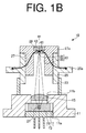
- FIG. 1A is a top view of the light-emitting device 10.
- FIG. 1B is a cross-sectional view of the light-emitting device 10 taken along line 1B-1B in FIG. 1A .
- a path of light emitting from a later-described light-emitting element in the light-emitting device 10 and entering a later-described light-transmitting member is indicated by a solid arrow (thinner line).
- An optical axis of the emitted light from the light-emitting element is indicated by "ax.”
- a heat dissipation path for heat generated in the later-described light-transmitting member is indicated by a solid arrow (thicker line).
- a base 11 can have a cylindrical hollow tubular shape, and include: a first inner wall portion 11a configured to support a stem 13; and a second inner wall portion 11b disposed in a region above the first inner wall portion 11a, configured to support a lens 15.
- the stem 13 can be fixed to the inner wall portion 11a of the base 11, for example, by means of welding or adhesive bonding.
- the stem 13 can be composed of a disk-shaped stem bottom 17 and a columnar stem cylinder 19 protruding from an upper surface of the stem bottom 17.
- a light-emitting element 21 can be a laser diode (LD) element which can emit laser light with a wavelength of 380 to 473 nm, preferably 445 nm, for example.
- the light-emitting element 21 can be disposed on the side surface of the stem cylinder 19 so as to emit light upwardly.
- the lens 15 can be disposed above the stem cylinder 19, i.e., in the light-emitting direction.
- the lens 15 can be fixed to the second inner wall portion 11b.
- the lens 15 can be, for example, a convex lens to converge the laser light emitted from the light-emitting element 21.
- a first tubular member 23 can be disposed above the lens 15 and can be a cylindrical member having a circular columnar hollow portion through which the laser light converged by the lens 15 can pass.
- the first tubular member 23 can be fixed to an upper surface of the base 11, for example, by means of welding or adhesive bonding.
- a second tubular member 25 can be a cylindrical member having a circular columnar hollow portion through which the laser light converged by the lens 15 can pass.
- the second tubular member 25 can include an annular heat-dissipating protrusion 25a protruded from an outer side surface thereof.
- the second tubular member 25 can be joined with the first tubular member 23 at a lower portion thereof in such a manner that an inner side surface of the first tubular member 23 can be in contact with the outer side surface of the second tubular member 25 to achieve fitting therebetween.
- the second tubular member 25 can be fixed to the first tubular member, for example, by means of welding or adhesive bonding.
- the heat-dissipating protrusion 25a can serve as a heat-dissipating part to be made in contact with a member (not shown) forming a heat dissipation path of the structure such as a heat-dissipating jig attached to the structure.
- the base 11, the first tubular member 23, and the second tubular member 25 can be made of a material with excellent thermal conductance, such as nickel, cobalt, iron, brass, stainless steel, a nickel-iron alloy, an iron-nickel-cobalt alloy, aluminum, copper, or carbon, for example.
- a holder 27 can be a cylindrical member having a recess 29 in an upper surface thereof.
- An incidence hole 31 with an elliptic column shape, through which the laser light converged by the lens 15 can pass, can be formed at the center of a bottom surface of the recess 29.
- a light-guiding hole 35, which can form a through hole 33 together with the incidence hole 31, can be formed below the incidence hole 31.
- the holder 27 can be a hollow cylindrical structure made of a single member.
- the holder 27 can be joined with the second tubular member 25 so as to achieve fitting therebetween in such a manner that an outer side surface of the holder 27 can be in contact with an inner side surface of the second tubular member 25.
- the holder 27 can include a flange 27a in an upper portion of the outer side surface thereof.
- the flange 27a can serve as a stopper when performing the insertion fitting of the holder 27 into the second tubular member 25.
- the holder 27 can be integrally molded with a material having excellent thermal conductance, such as nickel, cobalt, iron, brass, stainless steel, a nickel-iron alloy, an iron-nickel-cobalt alloy, aluminum, copper, or carbon, for example.
- a material having excellent thermal conductance such as nickel, cobalt, iron, brass, stainless steel, a nickel-iron alloy, an iron-nickel-cobalt alloy, aluminum, copper, or carbon, for example.
- a light-transmitting member 41 can be disposed at a central portion of the bottom surface of the recess 29 so as to block the incidence hole 31 and can be a member with a rectangular column shape, i.e., cuboid, having a rectangular bottom surface.
- the light-transmitting member 41 can be made of, for example, a light-transmitting material such as a glass, an aluminum oxide, a silicone resin, or an epoxy resin containing, as a wavelength conversion material, yellow phosphor particles of a YAG:Ce phosphor obtained by introducing Ce (cerium) as an activator into YAG (Yttrium Aluminum Garnet: Y 3 Al 5 O 12 ), or the like.
- a transparent adhesive such as a silicone resin adhesive or a glass adhesive, for example, can be used.
- the yellow phosphor can absorb laser light emitted from the light-emitting element 21, e.g., blue excitation light with a wavelength of about 460 nm and then emits yellow light having an emission peak wavelength of about 560 nm.
- white light can be obtained as a result of mixing blue light, which has been emitted from the light-emitting element 21 and has not been absorbed by the phosphor, and the yellow light emitted from the excited phosphor together.
- a phosphor which can emit other color may be used, if desired, without being limited to the yellow phosphor such as the above-described YAG:Ce.
- white light can be obtained by including a mixture of a red phosphor and a green phosphor in the light-transmitting member 41 and making these phosphors excited by blue laser light to mix the laser light and the fluorescence together.
- a laser element which can emit near-ultraviolet light with a wavelength of about 380 to 400 nm is used as the light-emitting element 21
- white light can be obtained by including a mixture of three kinds of phosphors which emit blue fluorescence, green fluorescence, and red fluorescence, respectively, when receiving light of this wavelength in the light-transmitting member 41 and making these phosphors excited by the laser light.
- light emission of a color other than white e.g., amber or red, can be obtained depending on a selection of phosphors to be used as appropriate.
- a reflective member 43 can be formed in the recess 29 so as to cover a side surface of the light-transmitting member 41.
- the reflective member 43 can be made of a silicone resin, an epoxy resin, or the like containing light-scattering particles of silica, alumina, titania, or the like.
- the reflective member 43 may be formed by: potting a resin material for forming the reflective member 43, which contains light-scattering particles, between an inner side surface of the recess 29 and the side surface of the light-transmitting member 41 after the light-transmitting member 41 is disposed in the recess 29; and thermally curing the resin material.
- a refractive index of a material forming the reflective member 43 be lower than a refractive index of a material forming the light-transmitting member 41 in order to make light, traveling from the light-transmitting member 41 toward the reflective member 43, totally reflected at an interface between the light-transmitting member 41 and the reflective member 43 and thereby avoid the light leaking into the reflective member 43 as much as possible.
- heat may be generated when the laser light emitted from the light-emitting element 21 and converged by the lens excites the phosphor in the light-transmitting member 41.
- This heat is generated more especially in a lower part of the light-transmitting member 41, i.e., in the vicinity of a surface (lower surface) through which the laser light is entered.
- the light-emitting device 10 can have the structure in which the holder 27 for holding the light-transmitting member 41 is fitted into the inner side of the second tubular member 25.
- a heat transfer structure serving also as a fixation (fitting) structure capable of being a heat transfer path can be provided in a large area below the light-transmitting member 41.
- a thermal resistance in the heat dissipation path can be reduced.
- a thermal resistance in the heat dissipation path can be reduced also by forming the holder 27 for holding the light-transmitting member 41 with a single member and thereby reducing the number of interfaces among members present along the heat dissipation path.
- the heat dissipation performance from the light-transmitting member 41 can be made excellent in the light-emitting device 10.
- a temperature of the light-transmitting member 41 can be kept low and a reduction in the excitation efficiency of the phosphor due to a temperature increase can be prevented.
- the holder 27 extend up to a region where the heat-dissipating protrusion 25a of the second tubular member 25 is formed and the outer side surface of the holder 27 be in contact with the inner side surface of the region where the heat-dissipating protrusion 25a of the second tubular member is formed.
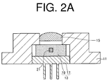
- the stem 13 equipped with the light-emitting element 21 can be fixed to the base 11 having the lens 15 attached thereto by means of welding or the like ( FIG. 2A ).
- the first tubular member 23 can be placed on the upper surface of the base 11 and the second tubular member 25 can be inserted and fitted into the first tubular member 23.
- the holder 27 can then be inserted and fitted into the second tubular member 25.
- the first tubular member 23 is not being fixed to the base 11 and movable in an in-plane direction (direction of an outline arrow in the figure) orthogonal to the optical axis ax.
- the second tubular member is not being fixed to the first tubular member 23.
- the second tubular member is movable in a direction along the optical axis ax (direction of a shaded arrow in the figure) and rotatable around the optical axis ax.
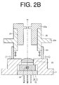
- the holder 27 is rotatable around the optical axis ax ( FIG. 2B ).
- the first tubular member 23 and the second tubular member 25 can be moved to make alignment in such a manner that a condensing point of light emitted from the light-emitting element 21 and condensed by the lens 15 coincides with the center of the upper surface of the incidence hole 31, i.e., the center of the bottom surface of the recess 29.
- the base 11 and the first tubular member 23 can be fixed together by means of welding or the like and the first tubular member 23 and the second tubular member 25 can be fixed together by means of welding or the like.
- the holder 27 is once removed from the second tubular member 25, and the light-transmitting member 41 can be fixed at the center of the bottom surface of the recess 29 so as to block the incidence hole 31.
- a transparent adhesive such as a silicone resin adhesive may be used.
- a resin material for forming the reflective member 43 which contains light-scattering particles, can be potted between the inner side surface of the recess 29 and the side surface of the light-transmitting member 41 and thermally cured.
- a silicone adhesive or the like containing a filler with high thermal conductance such as a silver filler, for example, can be applied to a region of the surface of the holder 27 to be in contact with the second tubular member 25 when fitting is performed. Then, the holder 27 can be inserted and fitted into the second tubular member 25. The holder 27 and the second tubular member 25 can be fixed together, for example, by thermally curing the applied adhesive.
- a lower surface of the flange 27a of the holder 27 and an upper surface of the second tubular member 25 can be welded together, for example, to complete the light-emitting device 10.
- the holder 27 is not screwed with, but is fitted into, the second tubular member 25. Therefore, the relative position between the holder 27 and the second tubular member 25, i.e., the relative position between the holder 27 and the light-emitting element 21 and the lens 15, when the light-emitting device 10 is completed, can be made coincide with the above-described aligned relative position with extremely high accuracy.
- the holder 27 is not screwed with, but fitted into, the second tubular member 25, rotational positions of the holder 27 and therefore the incidence hole 31 and the light-transmitting member 41 with respect to the optical axis ax can be very easily adjusted when precise orientation of the incidence hole 31 and/or the light-transmitting member 41 is required especially when the incidence hole 31 and/or the light-transmitting member 41 has a shape other than a circle in a top view as seen from above along the optical axis ax.
- the light-emitting device 10 can have the structure in which the holder 27 for holding the light-transmitting member 41 is fitted into the inner side of the second tubular member 25 and an area where the member capable of serving as a heat transfer path is present is thereby increased below the light-transmitting member 41.
- the heat transfer path from the lower surface of the light-transmitting member 41, which is a major heat generation source, to the heat-dissipating protrusion 25a can be shortened. A thermal resistance in the heat dissipation path can be thereby reduced.
- a thermal resistance in the heat dissipation path can be reduced also by forming the holder 27 for holding the light-transmitting member 41 with a single member and thereby reducing the number of interfaces among members present along the heat dissipation path. Therefore, a reduction in the excitation efficiency of the phosphor due to a temperature increase of the light-transmitting member 41 can be prevented.
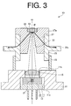
- FIG. 3 is a cross-sectional view of the light-emitting device 10 of the second exemplary embodiment made in accordance with the principles of the present invention. In FIG. 3 , as with FIG.
- a path of light emitting from the light-emitting element in the light-emitting device 10 and entering the light-transmitting member is indicated by a solid arrow (thinner line), and an optical axis of the emitted light from the light-emitting element is indicated by "ax.”
- a heat dissipation path for heat generated in the light-transmitting member is indicated by a solid arrow (thicker line).
- the light-guiding hole 35 of the through hole 33 can have a shape continuous with the incidence hole 31.
- the through hole 33 can have a circular truncated cone or elliptic truncated cone shape gradually narrowing in an upward direction up to the lower surface of the light-transmitting member 41 so as not to block a path of laser light emitted from the light-emitting element 21, condensed at the lens 15, and entered into the light-transmitting member 41.
- the through hole 33 can have a frustum shape in which as compared to one cross sectional shape on the light-emitting element 21 side, the other cross sectional shape opposite to the one cross sectional shape, i.e., the cross sectional shape in contact with the lower surface of the light-transmitting member 41, is smaller.
- the member containing a wavelength conversion material can be used as the light-transmitting member 41.
- the light-transmitting member 41 may contain a light-scattering material such as light-scattering particles of, for example, silica, alumina, titania, or the like. If there is no need to change the light color of laser light emitted from the light-emitting element 21, the light-transmitting member 41 may be a member containing only a light-scattering material without containing a wavelength conversion material.
- a light-scattering region 41a may be provided in a lower part of the light-transmitting member 41 and a wavelength conversion region 41b may be provided in an upper part of the light-transmitting member.
- the light-scattering region 41a may be made of, for example, a light-transmitting material containing light-scattering particles of silica, alumina, titania, or the like; and a light-transmitting ceramic material (glass, quartz, alumina, or the like), or a silicone resin or an epoxy resin.
- the wavelength conversion region 41b may be made of a light-transmitting material such as a glass, an aluminum oxide, a silicone resin, or an epoxy resin containing, as a wavelength conversion material, yellow phosphor particles of a YAG:Ce phosphor obtained by introducing Ce (cerium) as an activator into YAG (Yttrium Aluminum Garnet: Y 3 Al 5 O 12 ), or the like. While the light-scattering region 41a has been described as a region containing light-scattering particles, the light-scattering region 41a may be formed by roughening a surface of a light-transmitting material such as a ceramic, a light-transmitting resin, or a glass.
- a light-transmitting material such as a glass, an aluminum oxide, a silicone resin, or an epoxy resin containing, as a wavelength conversion material, yellow phosphor particles of a YAG:Ce phosphor obtained by introducing Ce (cerium) as an activator into YAG (
- the light-transmitting member 41 can have a rectangular column shape.
- the light-transmitting member 41 may have any other shape to change the shape of the light-emitting surface in accordance with the shape of irradiated light of the light-emitting device.
- the light-transmitting member 41 may have a circular column shape or a circular truncated cone shape.
- the light-transmitting member 41 may have an elliptic column shape or an elliptic truncated cone shape.
- the light-transmitting member 41 may have a polygonal column shape or a polygonal truncated cone shape.
- the incidence hole 31 can have an elliptic column shape or a circular truncated cone shape and the light-guiding hole 35 can have a circular column shape or a circular truncated cone shape.
- shapes of the incidence hole 31 and the light-guiding hole 35 can take various shapes such as an elliptic truncated cone shape, a polygonal column shape, and a polygonal truncated cone shape in addition to the above-described circular column shape, elliptic column shape, and circular truncated cone shape.
- an emission color of the light-emitting element and a fluorescent color of the phosphor can be freely selected depending on a desired color of emitted light, a usage thereof, and the like.
- the reflective member 43 can be provided so as to cover the side surface of the light-transmitting member 41 in the above-described exemplary embodiments, the reflective member 43 may not be formed.
Landscapes
- Physics & Mathematics (AREA)
- Optics & Photonics (AREA)
- Electromagnetism (AREA)
- General Physics & Mathematics (AREA)
- Condensed Matter Physics & Semiconductors (AREA)
- Engineering & Computer Science (AREA)
- Plasma & Fusion (AREA)
- Semiconductor Lasers (AREA)
Claims (3)
- Eine Licht emittierende Vorrichtung, die Folgendes aufweist:eine Basis (11);ein Licht emittierendes Element (21), das durch die Basis (11) gehalten wird;eine Linse (15), die durch die Basis (11) gehalten wird und über dem Licht emittierenden Element (21) angeordnet ist, die konfiguriert ist, um Licht, das von dem Licht emittierenden Element (21) emittiert wird, zu komprimieren bzw. zu sammeln;ein erstes rohrförmiges Glied (23), das auf der Basis (11) angeordnet ist;ein zweites rohrförmiges Glied (25), das in das erste rohrförmige Glied (23) eingepasst ist;einen Halter (27), der in das zweite rohrförmige Glied (25) eingesetzt ist und dadurch in das zweite rohrförmige Glied (25) eingepasst ist und ein Durchgangsloch (33) hat, durch welches Licht, das durch die Linse (15) gesammelt wird, hindurchtritt; undein Licht übertragendes Glied (41), das auf dem Halter (27) ausgebildet ist, um so das Durchgangsloch (33) zu verschließen; dadurch gekennzeichnet, dassdas zweite rohrförmige Glied (25) einen Wärmeableitungsteil hat, der auf einer äußeren Seitenfläche davon ausgebildet ist und von dieser hervorragt;der Halter (27) eine Struktur hat, die aus einem einzelnen Glied hergestellt ist, das aus einem oberen Flanschteil (27a) und einem unteren Einsetzpassteil besteht;der obere Flanschteil (27a) eine Unterseite hat, die auf einer Oberseite des zweiten rohrförmigen Gliedes (25) angeordnet ist; undsich der untere Einsetzpassteil des Halters (27) bis zu wenigstens einem Bereich erstreckt, in dem der Wärmeableitungsteil des zweiten rohrförmigen gliedes (25) ausgebildet ist und eine äußere Seitenfläche hat, die mit der inneren Seitenfläche des zweiten rohrförmigen Gliedes (25) in Kontakt ist.
- Licht emittierende Vorrichtung nach Anspruch 1, dadurch gekennzeichnet, dass das Durchgangsloch (33) eine Kegelstumpfform hat, so dass im Vergleich zu einer Querschnittsform näher an dem Licht emittierenden Element (21), die andere Querschnittsform gegenüber der einen Querschnittsform kleiner ist.
- Licht emittierende Vorrichtung nach Anspruch 1 oder 2, dadurch gekennzeichnet, dass der Wärmeableitungsteil eine ringförmige Form hat, die von der Außenfläche des zweiten rohrförmigen Gliedes (25) hervorsteht.
Applications Claiming Priority (1)
| Application Number | Priority Date | Filing Date | Title |
|---|---|---|---|
| JP2013053239A JP6103998B2 (ja) | 2013-03-15 | 2013-03-15 | 発光装置 |
Publications (2)
| Publication Number | Publication Date |
|---|---|
| EP2779331A1 EP2779331A1 (de) | 2014-09-17 |
| EP2779331B1 true EP2779331B1 (de) | 2016-11-30 |
Family
ID=50442320
Family Applications (1)
| Application Number | Title | Priority Date | Filing Date |
|---|---|---|---|
| EP14020031.2A Active EP2779331B1 (de) | 2013-03-15 | 2014-03-17 | Lichtemittierende Vorrichtung |
Country Status (4)
| Country | Link |
|---|---|
| US (1) | US9461433B2 (de) |
| EP (1) | EP2779331B1 (de) |
| JP (1) | JP6103998B2 (de) |
| KR (1) | KR102154644B1 (de) |
Families Citing this family (19)
| Publication number | Priority date | Publication date | Assignee | Title |
|---|---|---|---|---|
| JP6331353B2 (ja) | 2013-07-03 | 2018-05-30 | 日亜化学工業株式会社 | 発光装置 |
| US9768361B2 (en) * | 2014-07-23 | 2017-09-19 | Heptagon Micro Optics Pte. Ltd. | Light emitter and light detector modules including vertical alignment features |
| JP6303931B2 (ja) * | 2014-08-29 | 2018-04-04 | 日亜化学工業株式会社 | 発光装置 |
| JP2016092364A (ja) * | 2014-11-11 | 2016-05-23 | スタンレー電気株式会社 | 発光装置及び灯具 |
| JP6657559B2 (ja) * | 2014-12-24 | 2020-03-04 | 日亜化学工業株式会社 | 発光装置およびその製造方法 |
| JP6560902B2 (ja) * | 2015-05-26 | 2019-08-14 | スタンレー電気株式会社 | 光源装置及びこれを用いた照明装置 |
| US10475830B2 (en) | 2015-08-06 | 2019-11-12 | Ams Sensors Singapore Pte. Ltd. | Optical modules including customizable spacers for focal length adjustment and/or reduction of tilt, and fabrication of the optical modules |
| JP6493308B2 (ja) * | 2016-05-31 | 2019-04-03 | 日亜化学工業株式会社 | 発光装置 |
| JP6780377B2 (ja) * | 2016-08-30 | 2020-11-04 | 日亜化学工業株式会社 | 発光装置 |
| JP6776765B2 (ja) * | 2016-09-26 | 2020-10-28 | 日亜化学工業株式会社 | 発光装置 |
| KR102535603B1 (ko) * | 2017-08-04 | 2023-05-23 | 한국전자통신연구원 | 광 모듈 플랫폼 구조 및 제조방법 |
| DE102018203694B4 (de) | 2018-03-12 | 2021-12-23 | OSRAM Opto Semiconductors Gesellschaft mit beschränkter Haftung | Bestrahlungseinheit mit Pumpstrahlungsquelle und Konversionselement |
| JP6702349B2 (ja) * | 2018-03-27 | 2020-06-03 | 日亜化学工業株式会社 | 発光装置 |
| KR102025192B1 (ko) * | 2018-04-06 | 2019-09-25 | (주)제이스텍 | 하나의 조명에 의한 디스플레이 패널 및 cof 동시 촬상장치 |
| US11205886B2 (en) * | 2019-03-12 | 2021-12-21 | Nichia Corporation | Method of manufacturing optical member, optical member, and light emitting device |
| JP7568390B2 (ja) | 2019-09-20 | 2024-10-16 | 日亜化学工業株式会社 | 発光装置 |
| KR102394436B1 (ko) * | 2019-11-04 | 2022-05-03 | 한국전기연구원 | 광원 파장 변조 장치 |
| JP7104346B2 (ja) * | 2020-10-09 | 2022-07-21 | 日亜化学工業株式会社 | 発光装置 |
| CN112864794B (zh) * | 2021-01-21 | 2022-09-30 | 常州纵慧芯光半导体科技有限公司 | 一种激光设备及其控制方法 |
Family Cites Families (13)
| Publication number | Priority date | Publication date | Assignee | Title |
|---|---|---|---|---|
| US5739502A (en) * | 1983-12-27 | 1998-04-14 | General Electric Company | Laser intensity redistribution |
| JPS61207058U (de) * | 1985-06-18 | 1986-12-27 | ||
| US5111476A (en) * | 1991-02-21 | 1992-05-05 | Applied Laser Systems | Method and apparatus for aligning a laser diode, and laser diode system produced thereby |
| JP2002156563A (ja) * | 2000-11-22 | 2002-05-31 | Kyocera Corp | レセプタクル型光モジュール |
| JP2004004625A (ja) * | 2002-03-27 | 2004-01-08 | Matsushita Electric Ind Co Ltd | 光複合モジュール、光波長多重装置、光波長分離装置および光複合モジュール製造方法 |
| TW200306439A (en) | 2002-03-27 | 2003-11-16 | Matsushita Electric Industrial Co Ltd | Optical composite module, optical wavelength multiplexer, optical wavelength demutiplexer, and optical composite module manufacturing method |
| US6942372B1 (en) * | 2002-05-23 | 2005-09-13 | James M. Davis | Heat dissipating turret for fiberoptic illuminator |
| EP3540794B1 (de) * | 2006-03-10 | 2022-03-30 | Nichia Corporation | Lichtemittierende vorrichtung |
| EP1986028A3 (de) * | 2007-03-27 | 2008-11-05 | Rohm and Haas Electronic Materials LLC | Optische Anordnungen und Erzeugungsverfahren |
| JP2010040764A (ja) * | 2008-08-05 | 2010-02-18 | Nidec Sankyo Corp | レーザ加工装置 |
| JP5287275B2 (ja) * | 2009-01-15 | 2013-09-11 | 日亜化学工業株式会社 | 発光装置 |
| TWM399996U (en) * | 2010-09-28 | 2011-03-11 | Liverage Technology Inc | Optical fiber connector |
| US8888331B2 (en) | 2011-05-09 | 2014-11-18 | Microsoft Corporation | Low inductance light source module |
-
2013
- 2013-03-15 JP JP2013053239A patent/JP6103998B2/ja active Active
-
2014
- 2014-03-14 KR KR1020140030204A patent/KR102154644B1/ko active Active
- 2014-03-14 US US14/213,157 patent/US9461433B2/en active Active
- 2014-03-17 EP EP14020031.2A patent/EP2779331B1/de active Active
Also Published As
| Publication number | Publication date |
|---|---|
| US9461433B2 (en) | 2016-10-04 |
| KR20140113516A (ko) | 2014-09-24 |
| US20140268787A1 (en) | 2014-09-18 |
| JP6103998B2 (ja) | 2017-03-29 |
| JP2014179504A (ja) | 2014-09-25 |
| EP2779331A1 (de) | 2014-09-17 |
| KR102154644B1 (ko) | 2020-09-10 |
Similar Documents
| Publication | Publication Date | Title |
|---|---|---|
| EP2779331B1 (de) | Lichtemittierende Vorrichtung | |
| JP5287275B2 (ja) | 発光装置 | |
| JP6331353B2 (ja) | 発光装置 | |
| JP6115717B2 (ja) | 光源装置 | |
| EP2713410A1 (de) | Lichtemittierende Vorrichtung | |
| JP2012520565A (ja) | Ledリードフレームパッケージ、これを利用したledパッケージ及び前記ledパッケージの製造方法 | |
| KR20090023688A (ko) | 조명 장치 및 그 제조 방법 | |
| JP2015060871A (ja) | 発光装置 | |
| US10024505B2 (en) | Light emitting device | |
| JP5998962B2 (ja) | 半導体光装置 | |
| JP2004281606A (ja) | 発光装置およびその製造方法 | |
| US11499695B2 (en) | Optical member and light emission device | |
| JP6740766B2 (ja) | 光モジュール | |
| JP2017216362A (ja) | 発光装置 | |
| JP6819677B2 (ja) | 光モジュール | |
| JP2016162883A (ja) | 光モジュール | |
| JP6122674B2 (ja) | 波長変換装置 | |
| JP2020053372A (ja) | 発光装置の製造方法、発光モジュールの製造方法及び発光装置 | |
| WO2014156630A1 (ja) | 光通信用のレンズ及び光通信モジュール | |
| JP2015133231A (ja) | 光源装置 | |
| JP2011014852A (ja) | 発光装置 | |
| JP2014225608A (ja) | 発光装置 | |
| JP2013196786A (ja) | 発光装置及び照明装置 | |
| KR20120045876A (ko) | 발광소자 패키지 및 그 제조방법 | |
| JP2019159114A (ja) | 光モジュールの製造方法、及び、光モジュール |
Legal Events
| Date | Code | Title | Description |
|---|---|---|---|
| PUAI | Public reference made under article 153(3) epc to a published international application that has entered the european phase |
Free format text: ORIGINAL CODE: 0009012 |
|
| 17P | Request for examination filed |
Effective date: 20140317 |
|
| AK | Designated contracting states |
Kind code of ref document: A1 Designated state(s): AL AT BE BG CH CY CZ DE DK EE ES FI FR GB GR HR HU IE IS IT LI LT LU LV MC MK MT NL NO PL PT RO RS SE SI SK SM TR |
|
| AX | Request for extension of the european patent |
Extension state: BA ME |
|
| R17P | Request for examination filed (corrected) |
Effective date: 20150120 |
|
| RBV | Designated contracting states (corrected) |
Designated state(s): AL AT BE BG CH CY CZ DE DK EE ES FI FR GB GR HR HU IE IS IT LI LT LU LV MC MK MT NL NO PL PT RO RS SE SI SK SM TR |
|
| RIN1 | Information on inventor provided before grant (corrected) |
Inventor name: NOZAKI, TAKAHIKO |
|
| RIC1 | Information provided on ipc code assigned before grant |
Ipc: H01L 33/50 20100101ALI20160407BHEP Ipc: H01S 5/022 20060101ALI20160407BHEP Ipc: G02B 6/42 20060101ALI20160407BHEP Ipc: F21S 8/10 20060101ALI20160407BHEP Ipc: H01S 5/024 20060101ALI20160407BHEP Ipc: H01S 5/00 20060101AFI20160407BHEP |
|
| GRAP | Despatch of communication of intention to grant a patent |
Free format text: ORIGINAL CODE: EPIDOSNIGR1 |
|
| INTG | Intention to grant announced |
Effective date: 20160609 |
|
| GRAS | Grant fee paid |
Free format text: ORIGINAL CODE: EPIDOSNIGR3 |
|
| GRAA | (expected) grant |
Free format text: ORIGINAL CODE: 0009210 |
|
| AK | Designated contracting states |
Kind code of ref document: B1 Designated state(s): AL AT BE BG CH CY CZ DE DK EE ES FI FR GB GR HR HU IE IS IT LI LT LU LV MC MK MT NL NO PL PT RO RS SE SI SK SM TR |
|
| REG | Reference to a national code |
Ref country code: CH Ref legal event code: EP Ref country code: GB Ref legal event code: FG4D |
|
| REG | Reference to a national code |
Ref country code: AT Ref legal event code: REF Ref document number: 850619 Country of ref document: AT Kind code of ref document: T Effective date: 20161215 |
|
| REG | Reference to a national code |
Ref country code: IE Ref legal event code: FG4D |
|
| REG | Reference to a national code |
Ref country code: DE Ref legal event code: R096 Ref document number: 602014005094 Country of ref document: DE |
|
| REG | Reference to a national code |
Ref country code: FR Ref legal event code: PLFP Year of fee payment: 4 |
|
| PG25 | Lapsed in a contracting state [announced via postgrant information from national office to epo] |
Ref country code: LV Free format text: LAPSE BECAUSE OF FAILURE TO SUBMIT A TRANSLATION OF THE DESCRIPTION OR TO PAY THE FEE WITHIN THE PRESCRIBED TIME-LIMIT Effective date: 20161130 |
|
| REG | Reference to a national code |
Ref country code: LT Ref legal event code: MG4D |
|
| REG | Reference to a national code |
Ref country code: NL Ref legal event code: MP Effective date: 20161130 |
|
| REG | Reference to a national code |
Ref country code: AT Ref legal event code: MK05 Ref document number: 850619 Country of ref document: AT Kind code of ref document: T Effective date: 20161130 |
|
| PG25 | Lapsed in a contracting state [announced via postgrant information from national office to epo] |
Ref country code: GR Free format text: LAPSE BECAUSE OF FAILURE TO SUBMIT A TRANSLATION OF THE DESCRIPTION OR TO PAY THE FEE WITHIN THE PRESCRIBED TIME-LIMIT Effective date: 20170301 Ref country code: SE Free format text: LAPSE BECAUSE OF FAILURE TO SUBMIT A TRANSLATION OF THE DESCRIPTION OR TO PAY THE FEE WITHIN THE PRESCRIBED TIME-LIMIT Effective date: 20161130 Ref country code: LT Free format text: LAPSE BECAUSE OF FAILURE TO SUBMIT A TRANSLATION OF THE DESCRIPTION OR TO PAY THE FEE WITHIN THE PRESCRIBED TIME-LIMIT Effective date: 20161130 Ref country code: NO Free format text: LAPSE BECAUSE OF FAILURE TO SUBMIT A TRANSLATION OF THE DESCRIPTION OR TO PAY THE FEE WITHIN THE PRESCRIBED TIME-LIMIT Effective date: 20170228 |
|
| PG25 | Lapsed in a contracting state [announced via postgrant information from national office to epo] |
Ref country code: FI Free format text: LAPSE BECAUSE OF FAILURE TO SUBMIT A TRANSLATION OF THE DESCRIPTION OR TO PAY THE FEE WITHIN THE PRESCRIBED TIME-LIMIT Effective date: 20161130 Ref country code: RS Free format text: LAPSE BECAUSE OF FAILURE TO SUBMIT A TRANSLATION OF THE DESCRIPTION OR TO PAY THE FEE WITHIN THE PRESCRIBED TIME-LIMIT Effective date: 20161130 Ref country code: PT Free format text: LAPSE BECAUSE OF FAILURE TO SUBMIT A TRANSLATION OF THE DESCRIPTION OR TO PAY THE FEE WITHIN THE PRESCRIBED TIME-LIMIT Effective date: 20170330 Ref country code: HR Free format text: LAPSE BECAUSE OF FAILURE TO SUBMIT A TRANSLATION OF THE DESCRIPTION OR TO PAY THE FEE WITHIN THE PRESCRIBED TIME-LIMIT Effective date: 20161130 Ref country code: PL Free format text: LAPSE BECAUSE OF FAILURE TO SUBMIT A TRANSLATION OF THE DESCRIPTION OR TO PAY THE FEE WITHIN THE PRESCRIBED TIME-LIMIT Effective date: 20161130 Ref country code: AT Free format text: LAPSE BECAUSE OF FAILURE TO SUBMIT A TRANSLATION OF THE DESCRIPTION OR TO PAY THE FEE WITHIN THE PRESCRIBED TIME-LIMIT Effective date: 20161130 Ref country code: ES Free format text: LAPSE BECAUSE OF FAILURE TO SUBMIT A TRANSLATION OF THE DESCRIPTION OR TO PAY THE FEE WITHIN THE PRESCRIBED TIME-LIMIT Effective date: 20161130 |
|
| PG25 | Lapsed in a contracting state [announced via postgrant information from national office to epo] |
Ref country code: NL Free format text: LAPSE BECAUSE OF FAILURE TO SUBMIT A TRANSLATION OF THE DESCRIPTION OR TO PAY THE FEE WITHIN THE PRESCRIBED TIME-LIMIT Effective date: 20161130 |
|
| PG25 | Lapsed in a contracting state [announced via postgrant information from national office to epo] |
Ref country code: SK Free format text: LAPSE BECAUSE OF FAILURE TO SUBMIT A TRANSLATION OF THE DESCRIPTION OR TO PAY THE FEE WITHIN THE PRESCRIBED TIME-LIMIT Effective date: 20161130 Ref country code: EE Free format text: LAPSE BECAUSE OF FAILURE TO SUBMIT A TRANSLATION OF THE DESCRIPTION OR TO PAY THE FEE WITHIN THE PRESCRIBED TIME-LIMIT Effective date: 20161130 Ref country code: DK Free format text: LAPSE BECAUSE OF FAILURE TO SUBMIT A TRANSLATION OF THE DESCRIPTION OR TO PAY THE FEE WITHIN THE PRESCRIBED TIME-LIMIT Effective date: 20161130 Ref country code: RO Free format text: LAPSE BECAUSE OF FAILURE TO SUBMIT A TRANSLATION OF THE DESCRIPTION OR TO PAY THE FEE WITHIN THE PRESCRIBED TIME-LIMIT Effective date: 20161130 Ref country code: CZ Free format text: LAPSE BECAUSE OF FAILURE TO SUBMIT A TRANSLATION OF THE DESCRIPTION OR TO PAY THE FEE WITHIN THE PRESCRIBED TIME-LIMIT Effective date: 20161130 |
|
| PG25 | Lapsed in a contracting state [announced via postgrant information from national office to epo] |
Ref country code: BG Free format text: LAPSE BECAUSE OF FAILURE TO SUBMIT A TRANSLATION OF THE DESCRIPTION OR TO PAY THE FEE WITHIN THE PRESCRIBED TIME-LIMIT Effective date: 20170228 Ref country code: BE Free format text: LAPSE BECAUSE OF FAILURE TO SUBMIT A TRANSLATION OF THE DESCRIPTION OR TO PAY THE FEE WITHIN THE PRESCRIBED TIME-LIMIT Effective date: 20161130 Ref country code: IT Free format text: LAPSE BECAUSE OF FAILURE TO SUBMIT A TRANSLATION OF THE DESCRIPTION OR TO PAY THE FEE WITHIN THE PRESCRIBED TIME-LIMIT Effective date: 20161130 Ref country code: SM Free format text: LAPSE BECAUSE OF FAILURE TO SUBMIT A TRANSLATION OF THE DESCRIPTION OR TO PAY THE FEE WITHIN THE PRESCRIBED TIME-LIMIT Effective date: 20161130 |
|
| REG | Reference to a national code |
Ref country code: DE Ref legal event code: R097 Ref document number: 602014005094 Country of ref document: DE |
|
| PLBE | No opposition filed within time limit |
Free format text: ORIGINAL CODE: 0009261 |
|
| STAA | Information on the status of an ep patent application or granted ep patent |
Free format text: STATUS: NO OPPOSITION FILED WITHIN TIME LIMIT |
|
| REG | Reference to a national code |
Ref country code: CH Ref legal event code: PL |
|
| 26N | No opposition filed |
Effective date: 20170831 |
|
| PG25 | Lapsed in a contracting state [announced via postgrant information from national office to epo] |
Ref country code: SI Free format text: LAPSE BECAUSE OF FAILURE TO SUBMIT A TRANSLATION OF THE DESCRIPTION OR TO PAY THE FEE WITHIN THE PRESCRIBED TIME-LIMIT Effective date: 20161130 Ref country code: MC Free format text: LAPSE BECAUSE OF FAILURE TO SUBMIT A TRANSLATION OF THE DESCRIPTION OR TO PAY THE FEE WITHIN THE PRESCRIBED TIME-LIMIT Effective date: 20161130 |
|
| REG | Reference to a national code |
Ref country code: IE Ref legal event code: MM4A |
|
| PG25 | Lapsed in a contracting state [announced via postgrant information from national office to epo] |
Ref country code: LU Free format text: LAPSE BECAUSE OF NON-PAYMENT OF DUE FEES Effective date: 20170317 |
|
| REG | Reference to a national code |
Ref country code: FR Ref legal event code: PLFP Year of fee payment: 5 |
|
| PG25 | Lapsed in a contracting state [announced via postgrant information from national office to epo] |
Ref country code: CH Free format text: LAPSE BECAUSE OF NON-PAYMENT OF DUE FEES Effective date: 20170331 Ref country code: IE Free format text: LAPSE BECAUSE OF NON-PAYMENT OF DUE FEES Effective date: 20170317 Ref country code: LI Free format text: LAPSE BECAUSE OF NON-PAYMENT OF DUE FEES Effective date: 20170331 |
|
| PG25 | Lapsed in a contracting state [announced via postgrant information from national office to epo] |
Ref country code: MT Free format text: LAPSE BECAUSE OF NON-PAYMENT OF DUE FEES Effective date: 20170317 |
|
| PG25 | Lapsed in a contracting state [announced via postgrant information from national office to epo] |
Ref country code: HU Free format text: LAPSE BECAUSE OF FAILURE TO SUBMIT A TRANSLATION OF THE DESCRIPTION OR TO PAY THE FEE WITHIN THE PRESCRIBED TIME-LIMIT; INVALID AB INITIO Effective date: 20140317 |
|
| PG25 | Lapsed in a contracting state [announced via postgrant information from national office to epo] |
Ref country code: CY Free format text: LAPSE BECAUSE OF NON-PAYMENT OF DUE FEES Effective date: 20161130 |
|
| PG25 | Lapsed in a contracting state [announced via postgrant information from national office to epo] |
Ref country code: MK Free format text: LAPSE BECAUSE OF FAILURE TO SUBMIT A TRANSLATION OF THE DESCRIPTION OR TO PAY THE FEE WITHIN THE PRESCRIBED TIME-LIMIT Effective date: 20161130 |
|
| PG25 | Lapsed in a contracting state [announced via postgrant information from national office to epo] |
Ref country code: TR Free format text: LAPSE BECAUSE OF FAILURE TO SUBMIT A TRANSLATION OF THE DESCRIPTION OR TO PAY THE FEE WITHIN THE PRESCRIBED TIME-LIMIT Effective date: 20161130 |
|
| PG25 | Lapsed in a contracting state [announced via postgrant information from national office to epo] |
Ref country code: AL Free format text: LAPSE BECAUSE OF FAILURE TO SUBMIT A TRANSLATION OF THE DESCRIPTION OR TO PAY THE FEE WITHIN THE PRESCRIBED TIME-LIMIT Effective date: 20161130 Ref country code: IS Free format text: LAPSE BECAUSE OF FAILURE TO SUBMIT A TRANSLATION OF THE DESCRIPTION OR TO PAY THE FEE WITHIN THE PRESCRIBED TIME-LIMIT Effective date: 20170330 |
|
| PGFP | Annual fee paid to national office [announced via postgrant information from national office to epo] |
Ref country code: DE Payment date: 20250128 Year of fee payment: 12 |
|
| PGFP | Annual fee paid to national office [announced via postgrant information from national office to epo] |
Ref country code: FR Payment date: 20250210 Year of fee payment: 12 |
|
| PGFP | Annual fee paid to national office [announced via postgrant information from national office to epo] |
Ref country code: GB Payment date: 20250130 Year of fee payment: 12 |