EP2777083B1 - Procédé de mise en contact electrique d'un module électronique sous forme d'empilement et module électronique a structure de contact - Google Patents
Procédé de mise en contact electrique d'un module électronique sous forme d'empilement et module électronique a structure de contact Download PDFInfo
- Publication number
- EP2777083B1 EP2777083B1 EP13720962.3A EP13720962A EP2777083B1 EP 2777083 B1 EP2777083 B1 EP 2777083B1 EP 13720962 A EP13720962 A EP 13720962A EP 2777083 B1 EP2777083 B1 EP 2777083B1
- Authority
- EP
- European Patent Office
- Prior art keywords
- stack
- layers
- electrode layers
- electrode
- removal
- Prior art date
- Legal status (The legal status is an assumption and is not a legal conclusion. Google has not performed a legal analysis and makes no representation as to the accuracy of the status listed.)
- Active
Links
Images

Classifications
-
- H—ELECTRICITY
- H10—SEMICONDUCTOR DEVICES; ELECTRIC SOLID-STATE DEVICES NOT OTHERWISE PROVIDED FOR
- H10N—ELECTRIC SOLID-STATE DEVICES NOT OTHERWISE PROVIDED FOR
- H10N30/00—Piezoelectric or electrostrictive devices
- H10N30/50—Piezoelectric or electrostrictive devices having a stacked or multilayer structure
-
- B—PERFORMING OPERATIONS; TRANSPORTING
- B32—LAYERED PRODUCTS
- B32B—LAYERED PRODUCTS, i.e. PRODUCTS BUILT-UP OF STRATA OF FLAT OR NON-FLAT, e.g. CELLULAR OR HONEYCOMB, FORM
- B32B37/00—Methods or apparatus for laminating, e.g. by curing or by ultrasonic bonding
- B32B37/12—Methods or apparatus for laminating, e.g. by curing or by ultrasonic bonding characterised by using adhesives
-
- B—PERFORMING OPERATIONS; TRANSPORTING
- B32—LAYERED PRODUCTS
- B32B—LAYERED PRODUCTS, i.e. PRODUCTS BUILT-UP OF STRATA OF FLAT OR NON-FLAT, e.g. CELLULAR OR HONEYCOMB, FORM
- B32B38/00—Ancillary operations in connection with laminating processes
- B32B38/0008—Electrical discharge treatment, e.g. corona, plasma treatment; wave energy or particle radiation
-
- B—PERFORMING OPERATIONS; TRANSPORTING
- B32—LAYERED PRODUCTS
- B32B—LAYERED PRODUCTS, i.e. PRODUCTS BUILT-UP OF STRATA OF FLAT OR NON-FLAT, e.g. CELLULAR OR HONEYCOMB, FORM
- B32B38/00—Ancillary operations in connection with laminating processes
- B32B38/0012—Mechanical treatment, e.g. roughening, deforming, stretching
-
- H—ELECTRICITY
- H10—SEMICONDUCTOR DEVICES; ELECTRIC SOLID-STATE DEVICES NOT OTHERWISE PROVIDED FOR
- H10N—ELECTRIC SOLID-STATE DEVICES NOT OTHERWISE PROVIDED FOR
- H10N30/00—Piezoelectric or electrostrictive devices
- H10N30/01—Manufacture or treatment
- H10N30/05—Manufacture of multilayered piezoelectric or electrostrictive devices, or parts thereof, e.g. by stacking piezoelectric bodies and electrodes
- H10N30/057—Manufacture of multilayered piezoelectric or electrostrictive devices, or parts thereof, e.g. by stacking piezoelectric bodies and electrodes by stacking bulk piezoelectric or electrostrictive bodies and electrodes
-
- H—ELECTRICITY
- H10—SEMICONDUCTOR DEVICES; ELECTRIC SOLID-STATE DEVICES NOT OTHERWISE PROVIDED FOR
- H10N—ELECTRIC SOLID-STATE DEVICES NOT OTHERWISE PROVIDED FOR
- H10N30/00—Piezoelectric or electrostrictive devices
- H10N30/01—Manufacture or treatment
- H10N30/06—Forming electrodes or interconnections, e.g. leads or terminals
- H10N30/063—Forming interconnections, e.g. connection electrodes of multilayered piezoelectric or electrostrictive parts
-
- H—ELECTRICITY
- H10—SEMICONDUCTOR DEVICES; ELECTRIC SOLID-STATE DEVICES NOT OTHERWISE PROVIDED FOR
- H10N—ELECTRIC SOLID-STATE DEVICES NOT OTHERWISE PROVIDED FOR
- H10N30/00—Piezoelectric or electrostrictive devices
- H10N30/01—Manufacture or treatment
- H10N30/06—Forming electrodes or interconnections, e.g. leads or terminals
- H10N30/067—Forming single-layered electrodes of multilayered piezoelectric or electrostrictive parts
-
- H—ELECTRICITY
- H10—SEMICONDUCTOR DEVICES; ELECTRIC SOLID-STATE DEVICES NOT OTHERWISE PROVIDED FOR
- H10N—ELECTRIC SOLID-STATE DEVICES NOT OTHERWISE PROVIDED FOR
- H10N30/00—Piezoelectric or electrostrictive devices
- H10N30/01—Manufacture or treatment
- H10N30/08—Shaping or machining of piezoelectric or electrostrictive bodies
- H10N30/085—Shaping or machining of piezoelectric or electrostrictive bodies by machining
-
- H—ELECTRICITY
- H10—SEMICONDUCTOR DEVICES; ELECTRIC SOLID-STATE DEVICES NOT OTHERWISE PROVIDED FOR
- H10N—ELECTRIC SOLID-STATE DEVICES NOT OTHERWISE PROVIDED FOR
- H10N30/00—Piezoelectric or electrostrictive devices
- H10N30/80—Constructional details
- H10N30/87—Electrodes or interconnections, e.g. leads or terminals
- H10N30/871—Single-layered electrodes of multilayer piezoelectric or electrostrictive devices, e.g. internal electrodes
-
- H—ELECTRICITY
- H10—SEMICONDUCTOR DEVICES; ELECTRIC SOLID-STATE DEVICES NOT OTHERWISE PROVIDED FOR
- H10N—ELECTRIC SOLID-STATE DEVICES NOT OTHERWISE PROVIDED FOR
- H10N30/00—Piezoelectric or electrostrictive devices
- H10N30/80—Constructional details
- H10N30/87—Electrodes or interconnections, e.g. leads or terminals
- H10N30/872—Interconnections, e.g. connection electrodes of multilayer piezoelectric or electrostrictive devices
-
- B—PERFORMING OPERATIONS; TRANSPORTING
- B32—LAYERED PRODUCTS
- B32B—LAYERED PRODUCTS, i.e. PRODUCTS BUILT-UP OF STRATA OF FLAT OR NON-FLAT, e.g. CELLULAR OR HONEYCOMB, FORM
- B32B2307/00—Properties of the layers or laminate
- B32B2307/20—Properties of the layers or laminate having particular electrical or magnetic properties, e.g. piezoelectric
-
- B—PERFORMING OPERATIONS; TRANSPORTING
- B32—LAYERED PRODUCTS
- B32B—LAYERED PRODUCTS, i.e. PRODUCTS BUILT-UP OF STRATA OF FLAT OR NON-FLAT, e.g. CELLULAR OR HONEYCOMB, FORM
- B32B2310/00—Treatment by energy or chemical effects
- B32B2310/08—Treatment by energy or chemical effects by wave energy or particle radiation
- B32B2310/0806—Treatment by energy or chemical effects by wave energy or particle radiation using electromagnetic radiation
- B32B2310/0843—Treatment by energy or chemical effects by wave energy or particle radiation using electromagnetic radiation using laser
-
- B—PERFORMING OPERATIONS; TRANSPORTING
- B32—LAYERED PRODUCTS
- B32B—LAYERED PRODUCTS, i.e. PRODUCTS BUILT-UP OF STRATA OF FLAT OR NON-FLAT, e.g. CELLULAR OR HONEYCOMB, FORM
- B32B2310/00—Treatment by energy or chemical effects
- B32B2310/08—Treatment by energy or chemical effects by wave energy or particle radiation
- B32B2310/0875—Treatment by energy or chemical effects by wave energy or particle radiation using particle radiation
-
- B—PERFORMING OPERATIONS; TRANSPORTING
- B32—LAYERED PRODUCTS
- B32B—LAYERED PRODUCTS, i.e. PRODUCTS BUILT-UP OF STRATA OF FLAT OR NON-FLAT, e.g. CELLULAR OR HONEYCOMB, FORM
- B32B2311/00—Metals, their alloys or their compounds
-
- B—PERFORMING OPERATIONS; TRANSPORTING
- B32—LAYERED PRODUCTS
- B32B—LAYERED PRODUCTS, i.e. PRODUCTS BUILT-UP OF STRATA OF FLAT OR NON-FLAT, e.g. CELLULAR OR HONEYCOMB, FORM
- B32B2457/00—Electrical equipment
Definitions
- the invention relates to a method for electrically contacting an electronic component as a stack, which is formed from a plurality of reacting on application of an electric field material layers and a number of electrode layers, each material layer is disposed between two of the electrode layers, according to the preamble of claim 1
- the invention further relates to a stacked electronic component of the abovementioned type according to the preamble of claim 9.
- the most popular electronic component of this type today is a stack commonly referred to as a piezoactuator, which is used as an actuator in injection valves of a wide variety of engine types for motor vehicles.
- the material layers are ceramic layers in this piezoelectric actuator.
- such a stack viewed in plan view, has a rectangular or square cross-section.
- the stack is electrically contacted on two opposite circumferential sides.
- the electrode layers were geometrically designed in the past so that only every second electrode layer extends laterally to one of the two circumferential sides, while the respective other electrode layers do not extend to this peripheral side. The same applies analogously to the other circumferential side of the stack.
- a method of contacting a stacked piezoelectric device is known.
- this method alternately every other electrode layer is provided on both sides with an electrically insulating layer.
- the exposed electrode layers of each peripheral side are connected to each other via a conductive layer.
- a resin containing conductive particles is used as the conductive layer.
- a conductive adhesive comprises electrically conductive particles, for example of silver, gold or any other metal or a metal alloy, which are embedded in an insulating support material, for example a polyimide resin, an epoxy resin, etc.
- DE 10 2010 022 911 describes a method for producing a piezoelectric actuator with a piezoelectric stack and two outer electrodes arranged on the outside of the piezoelectric stack.
- the method according to the invention comprises the following steps: Provision of a fully active green stack comprising a plurality of alternately successive green sheets and continuous inner electrode layers, which are provided alternately electrically connected to two outer electrodes to be arranged on the outer side of the piezo stack to be produced from the green stack and electrically connected to the respective other outer electrode to be isolated; Providing the outside of the fully active green pile with trenches in areas where the internal electrode layers are to be electrically insulated from the corresponding external electrodes so that the trenches shorten the internal electrode layers in these areas inwardly from the outside of the green sheet; Filling the trenches with an electrically insulating slip; Further processing of the green pile whose trenches are filled with the slurry, so that the green sheets become piezoelectric layers and the green pile becomes the piezo stack; Applying the two outer
- DE 10 2008 049 788 A1 relates to an ultrasonic transducer with at least one monolithic, stacked piezoelectric element, which in the stacking direction an electrode layer, at least one further electrode layer and at least one between the Piezokeramik für arranged electrode layers, wherein the electrode layer extends to a side surface portion of the piezoelectric element and an outer electrode is disposed on the surface portion of the piezoelectric element such that the outer electrode on the surface portion selectively electrically connected to the electrode layer and selectively electrically isolated on the surface portion of the further electrode layer is.
- the ultrasonic transducer is characterized in that for the selective electrical contacting of the outer elec trode and the electrode layer with each other and for selective electrical insulation of the outer electrode and the further electrode layer from each other on the surface portion of a recess of the piezoelectric element is present, which is filled with electrical insulation material.
- the further electrode layer and the outer electrode are electrically isolated from each other.
- electrode material of an inner electrode of a ceramic bar is removed. The resulting recess is filled with insulation material. The ceramic bar is divided into individual piezo elements.
- GB 2 258 084 A discloses a laminated electromechanical transducer having a plurality of internal electrodes, wherein each second of the electrodes is electrically contacted and the other electrodes are electrically insulated by first removing electromechanical transducer material and the respective electrode and then filling the resulting trench with insulating material.
- a piezoelectric multilayer component is provided with a body in which piezoelectric layers and internal electrodes are arranged alternately, wherein at least one edge of the respective internal electrode opens into a depression formed on the surface of the body, which extends along this edge.
- JP 05 003 352 A a laminated piezoelectric actuator is described in which every other layer of piezoceramic and inner electrode are reset and the resulting trench is filled with an insulating material.
- JP 2005 079313A describes a laminated piezoactuator in which ceramic layers are superficially removed such that electrodes protrude into a trench formed thereby, wherein the ceramic layers have a convex shape between two adjacent electrodes as a result of the ablation process.
- the invention provides a method for electrically contacting an electronic component as a stack, which is formed from a plurality of reacting on application of an electric field material layers and a plurality of electrode layers, wherein each material layer between two of the electrode layers is arranged.
- An insulation structure is produced on at least one stack peripheral region of the stack, so that every second electrode layer of the at least one stack peripheral region is exposed for electrical contacting.
- Electrode layer at least partially covered by the insulation structure.
- the generation of the insulation structure and the exposure of each second electrode layer from the insulation structure can take place, for example, by first applying an insulation layer to the insulation layer Stacking peripheral region is applied, from which subsequently to expose every second electrode layer material is removed again.
- the insulation structure can also be applied via a direct structuring method, for example by means of spraying or dispensing, so that every second electrode layer remains free.
- a contacting structure is then applied to the at least one stack peripheral region provided with the insulation structure.
- the material of the material layers without removal of the material of the electrode layers is partially removed by means of a material-removing method such that the electrode layers are exposed near the surface.
- At least every second electrode layer is exposed near the surface as a result of the partial removal of the material layers, in particular each electrode layer exposed by the insulation structure.
- the advantage of the method according to the invention is that an enlarged surface for electrically contacting the electrode layers is available due to the exposure of the electrode layers close to the surface. As a result, a better electrical connection of the electrode layers to the contacting structure is possible. The risk of local excessive current densities and thus increased temperatures can be reduced thereby. As a result, the long-term reliability of the manufactured stack is improved.
- the removal of the material of the material layers takes place in such a way that near-surface portions of the electrode layers are at least partially exposed on their main surfaces in addition to their end face adjoining the stack peripheral region.
- the electrical contacting can thus take place not only on the end faces of the electrode layers, which are only a few microns wide. Instead, an additional contact area to the respective major surfaces are created.
- the size of the contacting region depends essentially on the chosen material-removing process and the duration of material removal.
- the stability of the thin electrode layers due to the removal of the material layers must not be weakened. It is sufficient if - starting from a surface formed by the stack peripheral areas - the material of the material layers is removed a few microns deep. In particular, the removal of the material of the material layers should not exceed a depth of 10 microns to 20 microns. At greater depths there is a risk that the electrode layers and the material of the material layers, which adjoins the electrodes, could be damaged in the further process of further processing.
- the partial, near-surface removal of the material of the material layers takes place before the step of generating the insulation structure.
- a respective stack perimeter area to which the outer electrodes are applied
- the near-surface partial removal of the material of the material layers takes place in order to expose the electrode layers approximately uniformly close to the surface.
- the partial, near-surface removal of the material of the material layers takes place after the step of generating the insulation structure.
- the exposure of each second electrode layer and the removal of the material of the material layers done by the same processing method.
- An advantage of this procedure is that no additional tools or processing steps must be provided in the context of the production of the component stack.
- the simultaneous exposure of each second electrode layer of the at least one stack peripheral region for electrical contacting and the removal of the material of the material layers in the exposed regions can be done, for example, using a laser.
- the partial, near-surface removal of the material of the material layers can be done for example by means of grinding, brushing, blasting or laser.
- the blasting may, for example, be by means of particles introduced into a carrier stream (e.g., sand).
- a carrier stream e.g., sand
- a thin metal layer in particular by sputtering, is applied to the stack peripheral region, onto which the contacting structure is applied to the thin metal layer in a subsequent step becomes.
- the thin metal layer allows a more reliable and defect-free contacting of the electrode layers of the stack. If the contacting structure, as is preferred, realized by means of a conductive adhesive, the metal particles contained in the conductive adhesive can electrically contact the thin metal layer in the region of the insulation structure and thus contribute in addition to a power line. Also by this the reliability of the electronic component can be increased.
- the invention further provides an electronic component designed as a stack.
- This comprises a plurality of electrode layers and a plurality of material layers reacting upon application of an electric field, wherein each material layer is arranged between two electrode layers.
- an insulation structure is provided, which is applied to at least one stack peripheral region of the stack, wherein the insulation structure is formed such that every second electrode layer of a stack peripheral region is exposed for electrical contacting.
- a contacting structure is applied to at least one stack peripheral region provided with the insulation structure.
- the stacked electronic component is characterized in that the material layers are at least partially removed in a section that is parallel to a longitudinal axis of the stack and perpendicularly through one of the stack peripheral regions in a region close to the surface that adjoins the electrode layers. in that the electrode layers are exposed both at their end face adjoining the stack peripheral region and at least partially at their opposing main surfaces, and are replaced by material of the insulation structure or the contacting structure.
- each second electrode layer is advantageously connected to the contacting structure.
- the near-surface region of the stack is to be understood as meaning a plane or surface of the stack circumferential region if the insulation structure and the contacting structure not yet applied to the stack perimeter area. After application, the insulation structure or the contacting structure adjoin the area near the surface of the material layers.
- the stack formed according to the invention has the same advantages as have been explained above in connection with the method according to the invention.
- the surface shape of the material layers processed by material removal is designed so that the material layers have a concave shape in a sectional view through the intersection between two adjacent electrode layers.
- the concave shape results from the material-removing process chosen for the machining.
- the material layers are reduced in regions relative to the stack peripheral region by at most 10 ⁇ m to 20 ⁇ m.
- This low material removal on the one hand enables improved contacting of the exposed sections of the electrode layers.
- the material reduction is so low that the further processing of the thus prepared stack requires no modification of the method steps for applying the insulation structure and the contacting structure. In particular, due to the low material removal, it can also be ensured that the surfaces of a finished stack are flat.
- the material of the contacting structure comprises a conductive adhesive with a support of a non-conductive material, in particular polyimide, and embedded therein metal particles.
- a conductive adhesive as the material for the contacting structure is that the non-conductive carrier material of the conductive adhesive has similar properties as the material used to produce the insulating structure. In this way, a high long-term reliability of the stack can be promoted, since high temperatures do not lead to different expansions of the insulation and the contacting structure. Furthermore, the risk of faulty contact points is reduced by the increased contact surface of the electrode layers.
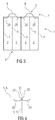
- the starting point is an electronic component designed as a stack 1.
- the stack 1 is formed from a plurality of material layers 2 reacting upon application of an electric field and a plurality of electrode layers 3, 4. Each of the material layers 2 is arranged between two of the electrode layers 3, 4.
- the electrode layers 3, 4 are guided on both sides to the respective edges of the stack 1.
- An electrical contacting takes place, for example, in interaction on opposite and geometrically non-contiguous stack circumferential regions 5, 6.
- the surfaces of the stack peripheral regions 5, 6 are generally ground to obtain planar surfaces for the further production steps.
- Such a stack 1 is in principle of the prior art known and used for example as a piezoelectric actuator for a piezoelectric injector for an internal combustion engine.
- an insulation structure 7 is applied to the stack circumferential region 5.
- the insulation structure 7 is structured such that the electrode layers 4 are exposed on the stack peripheral region 5.
- insulating walls 9 are applied to the electrode layers 3.
- their flanks extend obliquely in the direction of the component stack 1.
- the flanks could also be formed perpendicular to the plane of the stack perimeter region or curved, etc.
- an insulation structure 8 with insulating walls 10 is provided on the electrode layers 4 on the stack peripheral region 6.
- Flanks of the insulating walls 10 also extend only by way of example in the direction of the component stack 1, wherein the electrode layers 3 are exposed. It is obvious to a person skilled in the art that the flanks of the insulating walls 10 could also deviate from the shape shown.
- the generation of the isolation structures 7, 8 takes place, for example, by a subtractive method.
- a layer suitable for electrical insulation for example made of a polymer or a ceramic or a temperature-stable glass, is applied in a planar manner to the respective stack peripheral area 5, 6.
- a patterning process such as laser ablation or photopatterning
- every second of the electrode layers 3, 4 is opened on a respective stack perimeter area.
- the isolation structure can also be applied via a direct structuring method, for example by means of spraying or dispensing. If the material of the insulation structure is formed from a temperature-stable glass, it is expedient if this has a reduced silver migration. As a result, the insulating property of the glass is not adversely affected for a long period of time.
- the electrical contacting of the electrode layers 4 on the stack peripheral region 5 and the electrode layers 3 on the stack peripheral region 6 is realized by a contacting structure, which can be realized for example by means of a conductive adhesive.
- a conductive adhesive are in a non-conductive material, such. a resin of polyimide or epoxy, conductive metal particles introduced. Suitable materials are, in particular, gold, silver, palladium, platinum, copper or nickel and their alloys.
- the thickness of the contacting structure depends on the current carrying capacity of the contacting structure to be achieved.
- the contacting structures could also be formed from a metal or a metal alloy.
- a respective contacting structure 13, 14 thus assumes the electrical connection to the exposed electrode layers 3 and 4 and serves to conduct current with a predetermined current carrying capacity.
- the contacting structure 13, 14 thus forms respective outer electrodes.
- the electrode layers 4 are only a few microns, typically 1 to 4 microns, thick, especially when using a conductive adhesive as the material of the contacting structure there is a risk that some of the electrode layers or portions of electrode layers are not sufficiently electrically connected to the contacting structure. This results in a high contact resistance, so that locally excessive current densities and elevated temperatures can occur.
- the invention proposes to partially remove the material layers in such a way that the electrode layers are exposed near the surface before the contacting structure is produced by means of a material-removing method. This is for example in Fig. 2 represented, wherein the partial removal of the material of the material layers takes place here before applying the insulation structure.
- the removal of the material of the material layers can be done for example by means of grinding, brushing, blasting or by a laser.
- Will the stack perimeter areas 5, 6 (where in Fig. 2 only the stack perimeter area 5 is shown) is processed by means of sand blasting, the result, for example, between two adjacent electrode layers is a concave shape of the surfaces of the material layers 2 Fig. 2 Section shown here runs parallel to a longitudinal axis of the stack (which in Fig. 2 in sheet plane from left to right) and perpendicular through the stack perimeter area 5 (ie, in sheet plane from top to bottom).
- near-surface sections of the electrode layers 3, 4 are at least partially exposed at their opposite main surfaces 22, 23 in addition to their end face 21 adjoining the stack peripheral region 5, 6. This is increased and for only two adjacent material layers 2 in Fig. 4 shown.
- the depth T of material removal of the material of the material layers 2 is at most 10 .mu.m to 20 .mu.m, starting from the outermost end of an electrode layer 3, 4 to the lowest point of the machined material layer 2.
- the selected processing method is here in the area of the electrode layers under certain circumstances result in a lower material removal than, for example, in the middle between two electrode layers.
- only a few microns in the near-surface region of the electrode layers are freed from the material of the material layer 2.
- these exposed contact surfaces of the electrode layers are sufficient to provide a better electrical connection to the material of the contacting structure.
- Fig. 3 a section of a component stack 1 is shown, in which the production of the material removal 20 takes place only after the generation of the insulation structure 7.
- the exposure of the For the contacting structure required areas in the insulation 9 and the production of the material removal 20 can be done using the same processing method.
- the trenches can be produced in the isolation structure 7 with a laser. This can be further used to remove the material of the material layer 2 in the area between two walls 9, so that again the concave material erosion arise.
- the trenches in the insulation structure 7 and the production of the material erosions 20 in the material layers 2 can also be produced with different processing methods.
- the finished manufactured component stack has a planar surface.
- the proposed procedure is advantageous in particular in connection with the use of conductive adhesive as the material of the contacting structure, since after application of the material of the contacting structure, the metal particles contained in the conductive adhesive are randomly distributed. However, the larger the contact area available for the metal particles, the lower the risk that localized sites with high contact resistance will result.
Landscapes
- Engineering & Computer Science (AREA)
- Manufacturing & Machinery (AREA)
- Physics & Mathematics (AREA)
- Plasma & Fusion (AREA)
- Thermal Sciences (AREA)
- Mechanical Engineering (AREA)
- Fixed Capacitors And Capacitor Manufacturing Machines (AREA)
- Internal Circuitry In Semiconductor Integrated Circuit Devices (AREA)
- Manufacture Of Switches (AREA)
- Manufacturing Of Electrical Connectors (AREA)
- Coils Or Transformers For Communication (AREA)
Claims (11)
- Procédé pour la mise en contact électrique d'un module électronique sous forme d'empilement (1), qui est constitué d'une pluralité de couches de matériau (2) réagissant à l'application d'un champ électrique et d'une pluralité de couches d'électrodes (3, 4), chaque couche de matériau (2) étant disposée entre deux couches d'électrodes (3, 4), dans lequel procédé- sur au moins une zone périphérique (5, 6) de l'empilement (1) est générée une structure d'isolation (7, 8), moyennant quoi chaque deuxième couche d'électrodes (3, 4) de ladite au moins une zone périphérique (5, 6) de l'empilement est mise à nu pour la mise en contact électrique ;- une structure de mise en contact (13, 14) est déposée sur ladite au moins une zone périphérique (5, 6) de l'empilement munie de la structure d'isolation (7, 8) ;dans lequel- avant l'étape de la réalisation de la structure de mise en contact (13, 14), seul le matériau des couches de matériau (2) est enlevé partiellement au moyen d'un procédé par enlèvement de matière sans que les couches d'électrodes subissent un enlèvement de matière, de telle sorte qu'au moins chaque deuxième couche d'électrodes (3, 4) est mise à nu à proximité de la surface et de telle sorte que, sur une coupe qui s'étend parallèlement à un axe longitudinal de l'empilement (1) et perpendiculairement à travers l'une des zones périphériques (5, 6) de l'empilement, les couches de matériau (2) comportent une forme concave entre deux couches d'électrodes (3, 4) adjacentes, l'enlèvement de matière (20) dans les couches de matériau (2) étant plus faible dans la zone des couches d'électrodes (3, 4) qu'au milieu entre les deux couches d'électrodes (3, 4).
- Procédé selon la revendication 1, caractérisé en ce que l'enlèvement de matière dans les couches de matériau (2) est effectué de telle sorte que des parties proches de la surface dans les couches d'électrodes (3, 4) sont mises à nu, en plus de leurs faces frontales jouxtant la zone périphérique (5, 6) de l'empilement, au moins partiellement dans leurs surfaces principales.
- Procédé selon la revendication 1 ou 2, caractérisé en ce que l'enlèvement de matière partiel, proche de la surface, dans les couches de matériau (2) est effectué avant l'étape de la réalisation de la structure d'isolation.
- Procédé selon la revendication 1 ou 2, caractérisé en ce que l'enlèvement de matière partiel, proche de la surface, dans les couches de matériau (2) est effectué après l'étape de la réalisation de la structure d'isolation.
- Procédé selon la revendication 4, caractérisé en ce que la mise à nu de chaque deuxième couche d'électrodes (3, 4) de ladite au moins une zone périphérique (5, 6) de l'empilement en vue de la mise en contact électrique est effectuée en même temps que l'enlèvement de matière dans les couches de matériau (2) dans les zones mises à nu.
- Procédé selon la revendication 4 ou 5, caractérisé en ce que la mise à nu de chaque deuxième couche d'électrodes (3, 4) et l'enlèvement de matière dans les couches de matériau (2) sont effectués par le même procédé d'usinage.
- Siège de véhicule selon l'une quelconque des revendications précédentes, caractérisé en ce que l'enlèvement de matière partiel, proche de la surface, dans les couches de matériau (2) est effectué par meulage, décapage, rayonnement ou par un laser.
- Procédé selon l'une quelconque des revendications précédentes, caractérisé en ce que, après l'étape de la réalisation de la structure d'isolation (7, 8) et l'étape, éventuellement consécutive, de l'enlèvement de matière partiel dans les couches de matériau (2), une mince couche métallique est déposée, en particulier par pulvérisation cathodique, sur la zone périphérique (5, 6) de l'empilement, sur laquelle la structure de mise en contact (13, 14) est déposée sur la mince couche métallique au cours d'une étape consécutive.
- Module électronique réalisé sous la forme d'un empilement (1), comportent :- une pluralité de couches d'électrodes (3, 4) ;- une pluralité de couches de matériau (2) réagissant à l'application d'un champ électrique, chaque couche de matériau (2) étant disposée entre deux couches d'électrodes (3, 4) ;- une structure d'isolation (7, 8) qui est déposée sur au moins une zone périphérique (5, 6) de l'empilement (1), la structure d'isolation (7) étant réalisée de telle sorte que chaque deuxième couche d'électrodes (3, 4) d'une zone périphérique (5, 6) de l'empilement est mise à nu pour la mise en contact électrique ;- une structure de mise en contact (13, 14) déposée sur ladite au moins une zone périphérique (5, 6) de l'empilement munie de la structure d'isolation (7, 8) ;dans lequel- sur une coupe qui s'étend parallèlement à un axe longitudinal de l'empilement (1) et perpendiculairement à travers l'une des zones périphériques (5, 6) de l'empilement, les couches de matériau (2), au moins dans une zone proche de la surface qui jouxte les couches d'électrodes (3, 4) mises à nu, subissent au moins partiellement un enlèvement de matière, de telle sorte que les couches d'électrodes sont mises à nu tant sur leur face frontale jouxtant la zone périphérique de l'empilement que, au moins partiellement, sur leurs surfaces principales opposées, et sont remplacées par la matière de la structure d'isolation (7, 8) ou de la structure de mise en contact (13, 14),- sur la coupe qui s'étend parallèlement à un axe longitudinal de l'empilement (1) et perpendiculairement à travers l'une des zones périphériques (5, 6) de l'empilement, les couches de matériau (2) ont une forme concave entre deux couches d'électrodes (3, 4) adjacentes, caractérisé en ce que l'enlèvement de matière (20) dans les couches de matériau (2) est plus faible dans la zone des couches d'électrodes (3, 4) qu'au milieu entre les deux couches d'électrodes (3, 4).
- Empilement selon la revendication 9, caractérisé en ce que
les couches de matériau (2) en vis-à-vis la zone périphérique (5, 6) de l'empilement sont diminuées par zones de 10 µm à 20 µm au maximum. - Empilement selon la revendication 9 ou 10, caractérisé en ce que le matériau de la structure de mise en contact (13, 14) comporte une colle conductrice avec un support dans un matériau non conducteur, en particulier un polyimide, et des particules métalliques enrobées dans celui-ci.
Applications Claiming Priority (2)
| Application Number | Priority Date | Filing Date | Title |
|---|---|---|---|
| DE102012207598A DE102012207598A1 (de) | 2012-05-08 | 2012-05-08 | Verfahren zum elektrischen Kontaktieren eines elektronischen Bauelements als Stapel und elektronisches Bauelement mit einer Kontaktierungsstruktur |
| PCT/EP2013/059562 WO2013167643A2 (fr) | 2012-05-08 | 2013-05-08 | Procédé de mise en contact electrique d'un module électronique sous forme d'empilement et module électronique a structure de contact |
Publications (2)
| Publication Number | Publication Date |
|---|---|
| EP2777083A2 EP2777083A2 (fr) | 2014-09-17 |
| EP2777083B1 true EP2777083B1 (fr) | 2016-01-20 |
Family
ID=48325731
Family Applications (1)
| Application Number | Title | Priority Date | Filing Date |
|---|---|---|---|
| EP13720962.3A Active EP2777083B1 (fr) | 2012-05-08 | 2013-05-08 | Procédé de mise en contact electrique d'un module électronique sous forme d'empilement et module électronique a structure de contact |
Country Status (5)
| Country | Link |
|---|---|
| US (1) | US9691965B2 (fr) |
| EP (1) | EP2777083B1 (fr) |
| JP (1) | JP5875702B2 (fr) |
| DE (1) | DE102012207598A1 (fr) |
| WO (1) | WO2013167643A2 (fr) |
Families Citing this family (7)
| Publication number | Priority date | Publication date | Assignee | Title |
|---|---|---|---|---|
| JPWO2013157293A1 (ja) * | 2012-04-19 | 2015-12-21 | 日本碍子株式会社 | 膜型圧電/電歪素子 |
| DE102012207598A1 (de) * | 2012-05-08 | 2013-11-14 | Continental Automotive Gmbh | Verfahren zum elektrischen Kontaktieren eines elektronischen Bauelements als Stapel und elektronisches Bauelement mit einer Kontaktierungsstruktur |
| DE102015214778A1 (de) * | 2015-08-03 | 2017-02-09 | Continental Automotive Gmbh | Herstellungsverfahren zum Herstellen eines elektromechanischen Aktors und elektromechanischer Aktor |
| DE102015215204A1 (de) * | 2015-08-10 | 2017-02-16 | Continental Automotive Gmbh | Herstellungsverfahren zum Herstellen eines elektromechanischen Aktors und elektromechanischer Aktor. |
| DE102015217334B3 (de) * | 2015-09-10 | 2016-12-01 | Continental Automotive Gmbh | Verfahren zum Herstellen eines als Stapel ausgebildeten Vielschichtaktors |
| DE102016202839A1 (de) * | 2016-02-24 | 2017-03-09 | Continental Automotive Gmbh | Piezoelektrischer Schichtstapel und Verfahren zur Herstellung eines piezoelektrischen Schichtstapels |
| CN112518434B (zh) * | 2020-10-20 | 2021-10-01 | 陕西斯瑞新材料股份有限公司 | 一种CuCr触头物理法去毛刺的金属辅助加工工艺 |
Citations (1)
| Publication number | Priority date | Publication date | Assignee | Title |
|---|---|---|---|---|
| JP2005079313A (ja) * | 2003-08-29 | 2005-03-24 | Denso Corp | 積層型圧電素子の製造方法 |
Family Cites Families (21)
| Publication number | Priority date | Publication date | Assignee | Title |
|---|---|---|---|---|
| JPS62239588A (ja) * | 1986-04-10 | 1987-10-20 | Nagai Denshi Kogyo Kyodo Kumiai | 積層セラミツク圧電素子の製造方法 |
| WO1992005593A1 (fr) * | 1990-09-13 | 1992-04-02 | Hitachi Metals, Ltd. | Procede de fabrication d'elements possedant un effet d'electrostriction |
| JPH053352A (ja) * | 1991-06-04 | 1993-01-08 | Alps Electric Co Ltd | 積層型圧電アクチユエータおよびその製造方法 |
| JPH0529680A (ja) * | 1991-07-25 | 1993-02-05 | Hitachi Metals Ltd | 積層型変位素子およびその製造方法 |
| US5406164A (en) * | 1993-06-10 | 1995-04-11 | Brother Kogyo Kabushiki Kaisha | Multilayer piezoelectric element |
| JPH0774410A (ja) * | 1994-09-06 | 1995-03-17 | Ngk Spark Plug Co Ltd | 電歪積層板の製造方法 |
| JPH10223936A (ja) * | 1997-02-10 | 1998-08-21 | Minolta Co Ltd | 積層型圧電素子の製造方法 |
| JP3668072B2 (ja) * | 1999-09-28 | 2005-07-06 | 京セラ株式会社 | 積層型圧電アクチュエータ |
| JP2002203999A (ja) | 2000-11-06 | 2002-07-19 | Denso Corp | 積層型圧電体素子とその製造方法 |
| DE10112433A1 (de) * | 2001-03-15 | 2002-10-02 | Bosch Gmbh Robert | Messanordnung für eine Viskositätsmessung von Flüssigkeiten |
| JP3908157B2 (ja) * | 2002-01-24 | 2007-04-25 | Necエレクトロニクス株式会社 | フリップチップ型半導体装置の製造方法 |
| JP2004186507A (ja) * | 2002-12-04 | 2004-07-02 | Denso Corp | 積層型圧電素子及びその製造方法 |
| JP2005150167A (ja) * | 2003-11-11 | 2005-06-09 | Ibiden Co Ltd | 積層型圧電素子 |
| DE102006003070B3 (de) | 2006-01-20 | 2007-03-08 | Siemens Ag | Verfahren zum elektrischen Kontakieren eines elektronischen Bauelements |
| DE102006049323A1 (de) * | 2006-10-19 | 2008-04-24 | Epcos Ag | Piezoelektrisches Bauelement |
| DE102007004813B4 (de) * | 2007-01-31 | 2016-01-14 | Continental Automotive Gmbh | Verfahren zur Herstellung eines piezokeramischen Vielschichtaktors |
| DE102007058873A1 (de) * | 2007-12-06 | 2009-06-10 | Siemens Ag | Piezoelektrisches Bauteil mit Außenkontaktierung, die eine Gasphasen-Abscheidung aufweist, Verfahren zum Herstellen des Bauteils und Verwendung des Bauteils |
| DE102008049788A1 (de) * | 2008-09-30 | 2010-06-10 | Siemens Aktiengesellschaft | Ultraschallwandler mit mindestens einem vollaktiven, monolithischen Piezoelement, Verfahren zum selektiven Kontaktieren von Innenelektroden des Ultraschallwandlers durch Abtrag von Elektrodenmaterial und Verwendung des Utraschallwandlers |
| DE102010022911B4 (de) * | 2010-06-07 | 2017-01-19 | Continental Automotive Gmbh | Verfahren zum Herstellen eines Piezoaktors und Piezoaktor |
| DE102012207598A1 (de) * | 2012-05-08 | 2013-11-14 | Continental Automotive Gmbh | Verfahren zum elektrischen Kontaktieren eines elektronischen Bauelements als Stapel und elektronisches Bauelement mit einer Kontaktierungsstruktur |
| DE102012105287B4 (de) * | 2012-06-18 | 2020-07-02 | Tdk Electronics Ag | Verfahren zur Herstellung eines elektrischen Bauelements und Elektrisches Bauelement |
-
2012
- 2012-05-08 DE DE102012207598A patent/DE102012207598A1/de not_active Withdrawn
-
2013
- 2013-05-08 EP EP13720962.3A patent/EP2777083B1/fr active Active
- 2013-05-08 US US14/360,982 patent/US9691965B2/en active Active
- 2013-05-08 JP JP2014548111A patent/JP5875702B2/ja active Active
- 2013-05-08 WO PCT/EP2013/059562 patent/WO2013167643A2/fr not_active Ceased
Patent Citations (1)
| Publication number | Priority date | Publication date | Assignee | Title |
|---|---|---|---|---|
| JP2005079313A (ja) * | 2003-08-29 | 2005-03-24 | Denso Corp | 積層型圧電素子の製造方法 |
Also Published As
| Publication number | Publication date |
|---|---|
| WO2013167643A3 (fr) | 2014-06-19 |
| JP2015505165A (ja) | 2015-02-16 |
| DE102012207598A1 (de) | 2013-11-14 |
| JP5875702B2 (ja) | 2016-03-02 |
| EP2777083A2 (fr) | 2014-09-17 |
| US9691965B2 (en) | 2017-06-27 |
| US20150048722A1 (en) | 2015-02-19 |
| WO2013167643A2 (fr) | 2013-11-14 |
Similar Documents
| Publication | Publication Date | Title |
|---|---|---|
| EP2777083B1 (fr) | Procédé de mise en contact electrique d'un module électronique sous forme d'empilement et module électronique a structure de contact | |
| EP2126993B1 (fr) | Empilement piézoélectrique et procédé de fabrication d'un empilement piézoélectrique | |
| EP2126995A2 (fr) | Actionneur multicouche piézocéramique et procédé de fabrication associé | |
| EP1476907B1 (fr) | Actionneur piezo-electrique a electrode externe structuree | |
| EP2859566B1 (fr) | Procédé de fabrication d'un élément multicouche et élément multicouche | |
| EP2862185B1 (fr) | Procédé de fabrication d'un élément électrique | |
| EP2577762B1 (fr) | Procédé de fabrication d'un actionneur piézoélectrique et actionneur piézoélectrique | |
| DE102006003070B3 (de) | Verfahren zum elektrischen Kontakieren eines elektronischen Bauelements | |
| EP2543085B1 (fr) | Composant piézoélectrique | |
| EP2319102B1 (fr) | Piézoactionneur doté d'une couche de rupture préférentielle | |
| DE102008027115A1 (de) | Kontaktstruktur, elektronisches Bauelement mit einer Kontaktstruktur und Verfahren zu deren Herstellung | |
| EP2297797B1 (fr) | Composant piézoélectrique et procédé de fabrication d'un contact électrique | |
| EP2865027B1 (fr) | Procédé de fabrication d'un composant électronique sous la forme d'un empilage | |
| DE102009017434A1 (de) | Elektronisches Bauelement und Verfahren zum elektrischen Kontaktieren eines elektronischen Bauelements als Stapel | |
| EP2436050B1 (fr) | Composant piézoélectrique à couches multiples | |
| EP1821351B1 (fr) | Méthode pour produire un dispositif piézoélectrique | |
| EP2798679B1 (fr) | Pile piézo-électrique avec passivation et procédé de passivation d'une pile piézo-électrique | |
| DE112010002244T5 (de) | Piezoelektrische gestapelte Stellanordnung | |
| DE102017108384A1 (de) | Vielschichtbauelement und Verfahren zur Herstellung eines Vielschichtbauelements | |
| DE102006001656A1 (de) | Piezoaktor und Verfahren zur Herstellung desselben | |
| DE102010002818A1 (de) | Mikromechanisches Bauelement und Verfahren zur Herstellung eines mikromechanischen Bauelementes | |
| EP0358723B1 (fr) | Procédé de fabrication d'une tête piezoélectrique d'impression à l'encre | |
| DE102015217334B3 (de) | Verfahren zum Herstellen eines als Stapel ausgebildeten Vielschichtaktors | |
| DE102009014993A1 (de) | Verfahren zum elektrischen Kontaktieren eines elektronischen Bauelements | |
| EP3262698B1 (fr) | Procédé de fabrication de composants multicouches et composant multicouche |
Legal Events
| Date | Code | Title | Description |
|---|---|---|---|
| PUAI | Public reference made under article 153(3) epc to a published international application that has entered the european phase |
Free format text: ORIGINAL CODE: 0009012 |
|
| 17P | Request for examination filed |
Effective date: 20140612 |
|
| AK | Designated contracting states |
Kind code of ref document: A2 Designated state(s): AL AT BE BG CH CY CZ DE DK EE ES FI FR GB GR HR HU IE IS IT LI LT LU LV MC MK MT NL NO PL PT RO RS SE SI SK SM TR |
|
| 17Q | First examination report despatched |
Effective date: 20150305 |
|
| DAX | Request for extension of the european patent (deleted) | ||
| GRAP | Despatch of communication of intention to grant a patent |
Free format text: ORIGINAL CODE: EPIDOSNIGR1 |
|
| INTG | Intention to grant announced |
Effective date: 20150901 |
|
| GRAS | Grant fee paid |
Free format text: ORIGINAL CODE: EPIDOSNIGR3 |
|
| GRAA | (expected) grant |
Free format text: ORIGINAL CODE: 0009210 |
|
| AK | Designated contracting states |
Kind code of ref document: B1 Designated state(s): AL AT BE BG CH CY CZ DE DK EE ES FI FR GB GR HR HU IE IS IT LI LT LU LV MC MK MT NL NO PL PT RO RS SE SI SK SM TR |
|
| REG | Reference to a national code |
Ref country code: GB Ref legal event code: FG4D Free format text: NOT ENGLISH |
|
| REG | Reference to a national code |
Ref country code: CH Ref legal event code: EP |
|
| REG | Reference to a national code |
Ref country code: IE Ref legal event code: FG4D Free format text: LANGUAGE OF EP DOCUMENT: GERMAN |
|
| REG | Reference to a national code |
Ref country code: AT Ref legal event code: REF Ref document number: 772091 Country of ref document: AT Kind code of ref document: T Effective date: 20160215 |
|
| REG | Reference to a national code |
Ref country code: DE Ref legal event code: R096 Ref document number: 502013001856 Country of ref document: DE |
|
| REG | Reference to a national code |
Ref country code: FR Ref legal event code: PLFP Year of fee payment: 4 |
|
| REG | Reference to a national code |
Ref country code: LT Ref legal event code: MG4D Ref country code: NL Ref legal event code: MP Effective date: 20160120 |
|
| PG25 | Lapsed in a contracting state [announced via postgrant information from national office to epo] |
Ref country code: NL Free format text: LAPSE BECAUSE OF FAILURE TO SUBMIT A TRANSLATION OF THE DESCRIPTION OR TO PAY THE FEE WITHIN THE PRESCRIBED TIME-LIMIT Effective date: 20160120 |
|
| PG25 | Lapsed in a contracting state [announced via postgrant information from national office to epo] |
Ref country code: IT Free format text: LAPSE BECAUSE OF FAILURE TO SUBMIT A TRANSLATION OF THE DESCRIPTION OR TO PAY THE FEE WITHIN THE PRESCRIBED TIME-LIMIT Effective date: 20160120 Ref country code: GR Free format text: LAPSE BECAUSE OF FAILURE TO SUBMIT A TRANSLATION OF THE DESCRIPTION OR TO PAY THE FEE WITHIN THE PRESCRIBED TIME-LIMIT Effective date: 20160421 Ref country code: NO Free format text: LAPSE BECAUSE OF FAILURE TO SUBMIT A TRANSLATION OF THE DESCRIPTION OR TO PAY THE FEE WITHIN THE PRESCRIBED TIME-LIMIT Effective date: 20160420 Ref country code: FI Free format text: LAPSE BECAUSE OF FAILURE TO SUBMIT A TRANSLATION OF THE DESCRIPTION OR TO PAY THE FEE WITHIN THE PRESCRIBED TIME-LIMIT Effective date: 20160120 Ref country code: HR Free format text: LAPSE BECAUSE OF FAILURE TO SUBMIT A TRANSLATION OF THE DESCRIPTION OR TO PAY THE FEE WITHIN THE PRESCRIBED TIME-LIMIT Effective date: 20160120 Ref country code: ES Free format text: LAPSE BECAUSE OF FAILURE TO SUBMIT A TRANSLATION OF THE DESCRIPTION OR TO PAY THE FEE WITHIN THE PRESCRIBED TIME-LIMIT Effective date: 20160120 |
|
| PG25 | Lapsed in a contracting state [announced via postgrant information from national office to epo] |
Ref country code: PL Free format text: LAPSE BECAUSE OF FAILURE TO SUBMIT A TRANSLATION OF THE DESCRIPTION OR TO PAY THE FEE WITHIN THE PRESCRIBED TIME-LIMIT Effective date: 20160120 Ref country code: SE Free format text: LAPSE BECAUSE OF FAILURE TO SUBMIT A TRANSLATION OF THE DESCRIPTION OR TO PAY THE FEE WITHIN THE PRESCRIBED TIME-LIMIT Effective date: 20160120 Ref country code: LT Free format text: LAPSE BECAUSE OF FAILURE TO SUBMIT A TRANSLATION OF THE DESCRIPTION OR TO PAY THE FEE WITHIN THE PRESCRIBED TIME-LIMIT Effective date: 20160120 Ref country code: BE Free format text: LAPSE BECAUSE OF NON-PAYMENT OF DUE FEES Effective date: 20160531 Ref country code: PT Free format text: LAPSE BECAUSE OF FAILURE TO SUBMIT A TRANSLATION OF THE DESCRIPTION OR TO PAY THE FEE WITHIN THE PRESCRIBED TIME-LIMIT Effective date: 20160520 Ref country code: IS Free format text: LAPSE BECAUSE OF FAILURE TO SUBMIT A TRANSLATION OF THE DESCRIPTION OR TO PAY THE FEE WITHIN THE PRESCRIBED TIME-LIMIT Effective date: 20160520 Ref country code: RS Free format text: LAPSE BECAUSE OF FAILURE TO SUBMIT A TRANSLATION OF THE DESCRIPTION OR TO PAY THE FEE WITHIN THE PRESCRIBED TIME-LIMIT Effective date: 20160120 Ref country code: LV Free format text: LAPSE BECAUSE OF FAILURE TO SUBMIT A TRANSLATION OF THE DESCRIPTION OR TO PAY THE FEE WITHIN THE PRESCRIBED TIME-LIMIT Effective date: 20160120 |
|
| REG | Reference to a national code |
Ref country code: DE Ref legal event code: R097 Ref document number: 502013001856 Country of ref document: DE |
|
| PG25 | Lapsed in a contracting state [announced via postgrant information from national office to epo] |
Ref country code: EE Free format text: LAPSE BECAUSE OF FAILURE TO SUBMIT A TRANSLATION OF THE DESCRIPTION OR TO PAY THE FEE WITHIN THE PRESCRIBED TIME-LIMIT Effective date: 20160120 Ref country code: DK Free format text: LAPSE BECAUSE OF FAILURE TO SUBMIT A TRANSLATION OF THE DESCRIPTION OR TO PAY THE FEE WITHIN THE PRESCRIBED TIME-LIMIT Effective date: 20160120 |
|
| PLBE | No opposition filed within time limit |
Free format text: ORIGINAL CODE: 0009261 |
|
| STAA | Information on the status of an ep patent application or granted ep patent |
Free format text: STATUS: NO OPPOSITION FILED WITHIN TIME LIMIT |
|
| PG25 | Lapsed in a contracting state [announced via postgrant information from national office to epo] |
Ref country code: SM Free format text: LAPSE BECAUSE OF FAILURE TO SUBMIT A TRANSLATION OF THE DESCRIPTION OR TO PAY THE FEE WITHIN THE PRESCRIBED TIME-LIMIT Effective date: 20160120 Ref country code: CZ Free format text: LAPSE BECAUSE OF FAILURE TO SUBMIT A TRANSLATION OF THE DESCRIPTION OR TO PAY THE FEE WITHIN THE PRESCRIBED TIME-LIMIT Effective date: 20160120 Ref country code: SK Free format text: LAPSE BECAUSE OF FAILURE TO SUBMIT A TRANSLATION OF THE DESCRIPTION OR TO PAY THE FEE WITHIN THE PRESCRIBED TIME-LIMIT Effective date: 20160120 Ref country code: RO Free format text: LAPSE BECAUSE OF FAILURE TO SUBMIT A TRANSLATION OF THE DESCRIPTION OR TO PAY THE FEE WITHIN THE PRESCRIBED TIME-LIMIT Effective date: 20160120 |
|
| 26N | No opposition filed |
Effective date: 20161021 |
|
| PG25 | Lapsed in a contracting state [announced via postgrant information from national office to epo] |
Ref country code: LU Free format text: LAPSE BECAUSE OF FAILURE TO SUBMIT A TRANSLATION OF THE DESCRIPTION OR TO PAY THE FEE WITHIN THE PRESCRIBED TIME-LIMIT Effective date: 20160508 |
|
| REG | Reference to a national code |
Ref country code: CH Ref legal event code: PL |
|
| PG25 | Lapsed in a contracting state [announced via postgrant information from national office to epo] |
Ref country code: LI Free format text: LAPSE BECAUSE OF NON-PAYMENT OF DUE FEES Effective date: 20160531 Ref country code: CH Free format text: LAPSE BECAUSE OF NON-PAYMENT OF DUE FEES Effective date: 20160531 |
|
| REG | Reference to a national code |
Ref country code: IE Ref legal event code: MM4A |
|
| PG25 | Lapsed in a contracting state [announced via postgrant information from national office to epo] |
Ref country code: BG Free format text: LAPSE BECAUSE OF FAILURE TO SUBMIT A TRANSLATION OF THE DESCRIPTION OR TO PAY THE FEE WITHIN THE PRESCRIBED TIME-LIMIT Effective date: 20160420 Ref country code: SI Free format text: LAPSE BECAUSE OF FAILURE TO SUBMIT A TRANSLATION OF THE DESCRIPTION OR TO PAY THE FEE WITHIN THE PRESCRIBED TIME-LIMIT Effective date: 20160120 |
|
| REG | Reference to a national code |
Ref country code: FR Ref legal event code: PLFP Year of fee payment: 5 |
|
| PG25 | Lapsed in a contracting state [announced via postgrant information from national office to epo] |
Ref country code: IE Free format text: LAPSE BECAUSE OF NON-PAYMENT OF DUE FEES Effective date: 20160508 |
|
| REG | Reference to a national code |
Ref country code: FR Ref legal event code: PLFP Year of fee payment: 6 |
|
| PG25 | Lapsed in a contracting state [announced via postgrant information from national office to epo] |
Ref country code: HU Free format text: LAPSE BECAUSE OF FAILURE TO SUBMIT A TRANSLATION OF THE DESCRIPTION OR TO PAY THE FEE WITHIN THE PRESCRIBED TIME-LIMIT; INVALID AB INITIO Effective date: 20130508 |
|
| PG25 | Lapsed in a contracting state [announced via postgrant information from national office to epo] |
Ref country code: MT Free format text: LAPSE BECAUSE OF FAILURE TO SUBMIT A TRANSLATION OF THE DESCRIPTION OR TO PAY THE FEE WITHIN THE PRESCRIBED TIME-LIMIT Effective date: 20160120 Ref country code: MC Free format text: LAPSE BECAUSE OF FAILURE TO SUBMIT A TRANSLATION OF THE DESCRIPTION OR TO PAY THE FEE WITHIN THE PRESCRIBED TIME-LIMIT Effective date: 20160120 Ref country code: CY Free format text: LAPSE BECAUSE OF FAILURE TO SUBMIT A TRANSLATION OF THE DESCRIPTION OR TO PAY THE FEE WITHIN THE PRESCRIBED TIME-LIMIT Effective date: 20160120 Ref country code: MK Free format text: LAPSE BECAUSE OF FAILURE TO SUBMIT A TRANSLATION OF THE DESCRIPTION OR TO PAY THE FEE WITHIN THE PRESCRIBED TIME-LIMIT Effective date: 20160120 |
|
| PG25 | Lapsed in a contracting state [announced via postgrant information from national office to epo] |
Ref country code: AL Free format text: LAPSE BECAUSE OF FAILURE TO SUBMIT A TRANSLATION OF THE DESCRIPTION OR TO PAY THE FEE WITHIN THE PRESCRIBED TIME-LIMIT Effective date: 20160120 Ref country code: TR Free format text: LAPSE BECAUSE OF FAILURE TO SUBMIT A TRANSLATION OF THE DESCRIPTION OR TO PAY THE FEE WITHIN THE PRESCRIBED TIME-LIMIT Effective date: 20160120 |
|
| REG | Reference to a national code |
Ref country code: DE Ref legal event code: R081 Ref document number: 502013001856 Country of ref document: DE Owner name: VITESCO TECHNOLOGIES GMBH, DE Free format text: FORMER OWNER: CONTINENTAL AUTOMOTIVE GMBH, 30165 HANNOVER, DE |
|
| REG | Reference to a national code |
Ref country code: DE Ref legal event code: R081 Ref document number: 502013001856 Country of ref document: DE Owner name: SCHAEFFLER TECHNOLOGIES AG & CO. KG, DE Free format text: FORMER OWNER: VITESCO TECHNOLOGIES GMBH, 30165 HANNOVER, DE Ref country code: DE Ref legal event code: R081 Ref document number: 502013001856 Country of ref document: DE Owner name: VITESCO TECHNOLOGIES GMBH, DE Free format text: FORMER OWNER: VITESCO TECHNOLOGIES GMBH, 30165 HANNOVER, DE |
|
| REG | Reference to a national code |
Ref country code: DE Ref legal event code: R084 Ref document number: 502013001856 Country of ref document: DE |
|
| REG | Reference to a national code |
Ref country code: DE Ref legal event code: R079 Ref document number: 502013001856 Country of ref document: DE Free format text: PREVIOUS MAIN CLASS: H01L0041290000 Ipc: H10N0030060000 |
|
| REG | Reference to a national code |
Ref country code: GB Ref legal event code: 732E Free format text: REGISTERED BETWEEN 20230427 AND 20230503 |
|
| REG | Reference to a national code |
Ref country code: AT Ref legal event code: PC Ref document number: 772091 Country of ref document: AT Kind code of ref document: T Owner name: VITESCO TECHNOLOGIES GMBH, DE Effective date: 20230508 |
|
| P01 | Opt-out of the competence of the unified patent court (upc) registered |
Effective date: 20230530 |
|
| REG | Reference to a national code |
Ref country code: DE Ref legal event code: R081 Ref document number: 502013001856 Country of ref document: DE Owner name: SCHAEFFLER TECHNOLOGIES AG & CO. KG, DE Free format text: FORMER OWNER: VITESCO TECHNOLOGIES GMBH, 93055 REGENSBURG, DE |
|
| PGFP | Annual fee paid to national office [announced via postgrant information from national office to epo] |
Ref country code: DE Payment date: 20250531 Year of fee payment: 13 |
|
| PGFP | Annual fee paid to national office [announced via postgrant information from national office to epo] |
Ref country code: GB Payment date: 20250521 Year of fee payment: 13 |
|
| PGFP | Annual fee paid to national office [announced via postgrant information from national office to epo] |
Ref country code: FR Payment date: 20250528 Year of fee payment: 13 |
|
| PGFP | Annual fee paid to national office [announced via postgrant information from national office to epo] |
Ref country code: AT Payment date: 20250522 Year of fee payment: 13 |