EP2777083B1 - Method for making electrical contact with an electronic component in the form of a stack, and electronic component having a contact-making structure - Google Patents
Method for making electrical contact with an electronic component in the form of a stack, and electronic component having a contact-making structure Download PDFInfo
- Publication number
- EP2777083B1 EP2777083B1 EP13720962.3A EP13720962A EP2777083B1 EP 2777083 B1 EP2777083 B1 EP 2777083B1 EP 13720962 A EP13720962 A EP 13720962A EP 2777083 B1 EP2777083 B1 EP 2777083B1
- Authority
- EP
- European Patent Office
- Prior art keywords
- stack
- layers
- electrode layers
- electrode
- removal
- Prior art date
- Legal status (The legal status is an assumption and is not a legal conclusion. Google has not performed a legal analysis and makes no representation as to the accuracy of the status listed.)
- Active
Links
Images

Classifications
-
- H—ELECTRICITY
- H10—SEMICONDUCTOR DEVICES; ELECTRIC SOLID-STATE DEVICES NOT OTHERWISE PROVIDED FOR
- H10N—ELECTRIC SOLID-STATE DEVICES NOT OTHERWISE PROVIDED FOR
- H10N30/00—Piezoelectric or electrostrictive devices
- H10N30/50—Piezoelectric or electrostrictive devices having a stacked or multilayer structure
-
- B—PERFORMING OPERATIONS; TRANSPORTING
- B32—LAYERED PRODUCTS
- B32B—LAYERED PRODUCTS, i.e. PRODUCTS BUILT-UP OF STRATA OF FLAT OR NON-FLAT, e.g. CELLULAR OR HONEYCOMB, FORM
- B32B37/00—Methods or apparatus for laminating, e.g. by curing or by ultrasonic bonding
- B32B37/12—Methods or apparatus for laminating, e.g. by curing or by ultrasonic bonding characterised by using adhesives
-
- B—PERFORMING OPERATIONS; TRANSPORTING
- B32—LAYERED PRODUCTS
- B32B—LAYERED PRODUCTS, i.e. PRODUCTS BUILT-UP OF STRATA OF FLAT OR NON-FLAT, e.g. CELLULAR OR HONEYCOMB, FORM
- B32B38/00—Ancillary operations in connection with laminating processes
- B32B38/0008—Electrical discharge treatment, e.g. corona, plasma treatment; wave energy or particle radiation
-
- B—PERFORMING OPERATIONS; TRANSPORTING
- B32—LAYERED PRODUCTS
- B32B—LAYERED PRODUCTS, i.e. PRODUCTS BUILT-UP OF STRATA OF FLAT OR NON-FLAT, e.g. CELLULAR OR HONEYCOMB, FORM
- B32B38/00—Ancillary operations in connection with laminating processes
- B32B38/0012—Mechanical treatment, e.g. roughening, deforming, stretching
-
- H—ELECTRICITY
- H10—SEMICONDUCTOR DEVICES; ELECTRIC SOLID-STATE DEVICES NOT OTHERWISE PROVIDED FOR
- H10N—ELECTRIC SOLID-STATE DEVICES NOT OTHERWISE PROVIDED FOR
- H10N30/00—Piezoelectric or electrostrictive devices
- H10N30/01—Manufacture or treatment
- H10N30/05—Manufacture of multilayered piezoelectric or electrostrictive devices, or parts thereof, e.g. by stacking piezoelectric bodies and electrodes
- H10N30/057—Manufacture of multilayered piezoelectric or electrostrictive devices, or parts thereof, e.g. by stacking piezoelectric bodies and electrodes by stacking bulk piezoelectric or electrostrictive bodies and electrodes
-
- H—ELECTRICITY
- H10—SEMICONDUCTOR DEVICES; ELECTRIC SOLID-STATE DEVICES NOT OTHERWISE PROVIDED FOR
- H10N—ELECTRIC SOLID-STATE DEVICES NOT OTHERWISE PROVIDED FOR
- H10N30/00—Piezoelectric or electrostrictive devices
- H10N30/01—Manufacture or treatment
- H10N30/06—Forming electrodes or interconnections, e.g. leads or terminals
- H10N30/063—Forming interconnections, e.g. connection electrodes of multilayered piezoelectric or electrostrictive parts
-
- H—ELECTRICITY
- H10—SEMICONDUCTOR DEVICES; ELECTRIC SOLID-STATE DEVICES NOT OTHERWISE PROVIDED FOR
- H10N—ELECTRIC SOLID-STATE DEVICES NOT OTHERWISE PROVIDED FOR
- H10N30/00—Piezoelectric or electrostrictive devices
- H10N30/01—Manufacture or treatment
- H10N30/06—Forming electrodes or interconnections, e.g. leads or terminals
- H10N30/067—Forming single-layered electrodes of multilayered piezoelectric or electrostrictive parts
-
- H—ELECTRICITY
- H10—SEMICONDUCTOR DEVICES; ELECTRIC SOLID-STATE DEVICES NOT OTHERWISE PROVIDED FOR
- H10N—ELECTRIC SOLID-STATE DEVICES NOT OTHERWISE PROVIDED FOR
- H10N30/00—Piezoelectric or electrostrictive devices
- H10N30/01—Manufacture or treatment
- H10N30/08—Shaping or machining of piezoelectric or electrostrictive bodies
- H10N30/085—Shaping or machining of piezoelectric or electrostrictive bodies by machining
-
- H—ELECTRICITY
- H10—SEMICONDUCTOR DEVICES; ELECTRIC SOLID-STATE DEVICES NOT OTHERWISE PROVIDED FOR
- H10N—ELECTRIC SOLID-STATE DEVICES NOT OTHERWISE PROVIDED FOR
- H10N30/00—Piezoelectric or electrostrictive devices
- H10N30/80—Constructional details
- H10N30/87—Electrodes or interconnections, e.g. leads or terminals
- H10N30/871—Single-layered electrodes of multilayer piezoelectric or electrostrictive devices, e.g. internal electrodes
-
- H—ELECTRICITY
- H10—SEMICONDUCTOR DEVICES; ELECTRIC SOLID-STATE DEVICES NOT OTHERWISE PROVIDED FOR
- H10N—ELECTRIC SOLID-STATE DEVICES NOT OTHERWISE PROVIDED FOR
- H10N30/00—Piezoelectric or electrostrictive devices
- H10N30/80—Constructional details
- H10N30/87—Electrodes or interconnections, e.g. leads or terminals
- H10N30/872—Interconnections, e.g. connection electrodes of multilayer piezoelectric or electrostrictive devices
-
- B—PERFORMING OPERATIONS; TRANSPORTING
- B32—LAYERED PRODUCTS
- B32B—LAYERED PRODUCTS, i.e. PRODUCTS BUILT-UP OF STRATA OF FLAT OR NON-FLAT, e.g. CELLULAR OR HONEYCOMB, FORM
- B32B2307/00—Properties of the layers or laminate
- B32B2307/20—Properties of the layers or laminate having particular electrical or magnetic properties, e.g. piezoelectric
-
- B—PERFORMING OPERATIONS; TRANSPORTING
- B32—LAYERED PRODUCTS
- B32B—LAYERED PRODUCTS, i.e. PRODUCTS BUILT-UP OF STRATA OF FLAT OR NON-FLAT, e.g. CELLULAR OR HONEYCOMB, FORM
- B32B2310/00—Treatment by energy or chemical effects
- B32B2310/08—Treatment by energy or chemical effects by wave energy or particle radiation
- B32B2310/0806—Treatment by energy or chemical effects by wave energy or particle radiation using electromagnetic radiation
- B32B2310/0843—Treatment by energy or chemical effects by wave energy or particle radiation using electromagnetic radiation using laser
-
- B—PERFORMING OPERATIONS; TRANSPORTING
- B32—LAYERED PRODUCTS
- B32B—LAYERED PRODUCTS, i.e. PRODUCTS BUILT-UP OF STRATA OF FLAT OR NON-FLAT, e.g. CELLULAR OR HONEYCOMB, FORM
- B32B2310/00—Treatment by energy or chemical effects
- B32B2310/08—Treatment by energy or chemical effects by wave energy or particle radiation
- B32B2310/0875—Treatment by energy or chemical effects by wave energy or particle radiation using particle radiation
-
- B—PERFORMING OPERATIONS; TRANSPORTING
- B32—LAYERED PRODUCTS
- B32B—LAYERED PRODUCTS, i.e. PRODUCTS BUILT-UP OF STRATA OF FLAT OR NON-FLAT, e.g. CELLULAR OR HONEYCOMB, FORM
- B32B2311/00—Metals, their alloys or their compounds
-
- B—PERFORMING OPERATIONS; TRANSPORTING
- B32—LAYERED PRODUCTS
- B32B—LAYERED PRODUCTS, i.e. PRODUCTS BUILT-UP OF STRATA OF FLAT OR NON-FLAT, e.g. CELLULAR OR HONEYCOMB, FORM
- B32B2457/00—Electrical equipment
Definitions
- the invention relates to a method for electrically contacting an electronic component as a stack, which is formed from a plurality of reacting on application of an electric field material layers and a number of electrode layers, each material layer is disposed between two of the electrode layers, according to the preamble of claim 1
- the invention further relates to a stacked electronic component of the abovementioned type according to the preamble of claim 9.
- the most popular electronic component of this type today is a stack commonly referred to as a piezoactuator, which is used as an actuator in injection valves of a wide variety of engine types for motor vehicles.
- the material layers are ceramic layers in this piezoelectric actuator.
- such a stack viewed in plan view, has a rectangular or square cross-section.
- the stack is electrically contacted on two opposite circumferential sides.
- the electrode layers were geometrically designed in the past so that only every second electrode layer extends laterally to one of the two circumferential sides, while the respective other electrode layers do not extend to this peripheral side. The same applies analogously to the other circumferential side of the stack.
- a method of contacting a stacked piezoelectric device is known.
- this method alternately every other electrode layer is provided on both sides with an electrically insulating layer.
- the exposed electrode layers of each peripheral side are connected to each other via a conductive layer.
- a resin containing conductive particles is used as the conductive layer.
- a conductive adhesive comprises electrically conductive particles, for example of silver, gold or any other metal or a metal alloy, which are embedded in an insulating support material, for example a polyimide resin, an epoxy resin, etc.
- DE 10 2010 022 911 describes a method for producing a piezoelectric actuator with a piezoelectric stack and two outer electrodes arranged on the outside of the piezoelectric stack.
- the method according to the invention comprises the following steps: Provision of a fully active green stack comprising a plurality of alternately successive green sheets and continuous inner electrode layers, which are provided alternately electrically connected to two outer electrodes to be arranged on the outer side of the piezo stack to be produced from the green stack and electrically connected to the respective other outer electrode to be isolated; Providing the outside of the fully active green pile with trenches in areas where the internal electrode layers are to be electrically insulated from the corresponding external electrodes so that the trenches shorten the internal electrode layers in these areas inwardly from the outside of the green sheet; Filling the trenches with an electrically insulating slip; Further processing of the green pile whose trenches are filled with the slurry, so that the green sheets become piezoelectric layers and the green pile becomes the piezo stack; Applying the two outer
- DE 10 2008 049 788 A1 relates to an ultrasonic transducer with at least one monolithic, stacked piezoelectric element, which in the stacking direction an electrode layer, at least one further electrode layer and at least one between the Piezokeramik für arranged electrode layers, wherein the electrode layer extends to a side surface portion of the piezoelectric element and an outer electrode is disposed on the surface portion of the piezoelectric element such that the outer electrode on the surface portion selectively electrically connected to the electrode layer and selectively electrically isolated on the surface portion of the further electrode layer is.
- the ultrasonic transducer is characterized in that for the selective electrical contacting of the outer elec trode and the electrode layer with each other and for selective electrical insulation of the outer electrode and the further electrode layer from each other on the surface portion of a recess of the piezoelectric element is present, which is filled with electrical insulation material.
- the further electrode layer and the outer electrode are electrically isolated from each other.
- electrode material of an inner electrode of a ceramic bar is removed. The resulting recess is filled with insulation material. The ceramic bar is divided into individual piezo elements.
- GB 2 258 084 A discloses a laminated electromechanical transducer having a plurality of internal electrodes, wherein each second of the electrodes is electrically contacted and the other electrodes are electrically insulated by first removing electromechanical transducer material and the respective electrode and then filling the resulting trench with insulating material.
- a piezoelectric multilayer component is provided with a body in which piezoelectric layers and internal electrodes are arranged alternately, wherein at least one edge of the respective internal electrode opens into a depression formed on the surface of the body, which extends along this edge.
- JP 05 003 352 A a laminated piezoelectric actuator is described in which every other layer of piezoceramic and inner electrode are reset and the resulting trench is filled with an insulating material.
- JP 2005 079313A describes a laminated piezoactuator in which ceramic layers are superficially removed such that electrodes protrude into a trench formed thereby, wherein the ceramic layers have a convex shape between two adjacent electrodes as a result of the ablation process.
- the invention provides a method for electrically contacting an electronic component as a stack, which is formed from a plurality of reacting on application of an electric field material layers and a plurality of electrode layers, wherein each material layer between two of the electrode layers is arranged.
- An insulation structure is produced on at least one stack peripheral region of the stack, so that every second electrode layer of the at least one stack peripheral region is exposed for electrical contacting.
- Electrode layer at least partially covered by the insulation structure.
- the generation of the insulation structure and the exposure of each second electrode layer from the insulation structure can take place, for example, by first applying an insulation layer to the insulation layer Stacking peripheral region is applied, from which subsequently to expose every second electrode layer material is removed again.
- the insulation structure can also be applied via a direct structuring method, for example by means of spraying or dispensing, so that every second electrode layer remains free.
- a contacting structure is then applied to the at least one stack peripheral region provided with the insulation structure.
- the material of the material layers without removal of the material of the electrode layers is partially removed by means of a material-removing method such that the electrode layers are exposed near the surface.
- At least every second electrode layer is exposed near the surface as a result of the partial removal of the material layers, in particular each electrode layer exposed by the insulation structure.
- the advantage of the method according to the invention is that an enlarged surface for electrically contacting the electrode layers is available due to the exposure of the electrode layers close to the surface. As a result, a better electrical connection of the electrode layers to the contacting structure is possible. The risk of local excessive current densities and thus increased temperatures can be reduced thereby. As a result, the long-term reliability of the manufactured stack is improved.
- the removal of the material of the material layers takes place in such a way that near-surface portions of the electrode layers are at least partially exposed on their main surfaces in addition to their end face adjoining the stack peripheral region.
- the electrical contacting can thus take place not only on the end faces of the electrode layers, which are only a few microns wide. Instead, an additional contact area to the respective major surfaces are created.
- the size of the contacting region depends essentially on the chosen material-removing process and the duration of material removal.
- the stability of the thin electrode layers due to the removal of the material layers must not be weakened. It is sufficient if - starting from a surface formed by the stack peripheral areas - the material of the material layers is removed a few microns deep. In particular, the removal of the material of the material layers should not exceed a depth of 10 microns to 20 microns. At greater depths there is a risk that the electrode layers and the material of the material layers, which adjoins the electrodes, could be damaged in the further process of further processing.
- the partial, near-surface removal of the material of the material layers takes place before the step of generating the insulation structure.
- a respective stack perimeter area to which the outer electrodes are applied
- the near-surface partial removal of the material of the material layers takes place in order to expose the electrode layers approximately uniformly close to the surface.
- the partial, near-surface removal of the material of the material layers takes place after the step of generating the insulation structure.
- the exposure of each second electrode layer and the removal of the material of the material layers done by the same processing method.
- An advantage of this procedure is that no additional tools or processing steps must be provided in the context of the production of the component stack.
- the simultaneous exposure of each second electrode layer of the at least one stack peripheral region for electrical contacting and the removal of the material of the material layers in the exposed regions can be done, for example, using a laser.
- the partial, near-surface removal of the material of the material layers can be done for example by means of grinding, brushing, blasting or laser.
- the blasting may, for example, be by means of particles introduced into a carrier stream (e.g., sand).
- a carrier stream e.g., sand
- a thin metal layer in particular by sputtering, is applied to the stack peripheral region, onto which the contacting structure is applied to the thin metal layer in a subsequent step becomes.
- the thin metal layer allows a more reliable and defect-free contacting of the electrode layers of the stack. If the contacting structure, as is preferred, realized by means of a conductive adhesive, the metal particles contained in the conductive adhesive can electrically contact the thin metal layer in the region of the insulation structure and thus contribute in addition to a power line. Also by this the reliability of the electronic component can be increased.
- the invention further provides an electronic component designed as a stack.
- This comprises a plurality of electrode layers and a plurality of material layers reacting upon application of an electric field, wherein each material layer is arranged between two electrode layers.
- an insulation structure is provided, which is applied to at least one stack peripheral region of the stack, wherein the insulation structure is formed such that every second electrode layer of a stack peripheral region is exposed for electrical contacting.
- a contacting structure is applied to at least one stack peripheral region provided with the insulation structure.
- the stacked electronic component is characterized in that the material layers are at least partially removed in a section that is parallel to a longitudinal axis of the stack and perpendicularly through one of the stack peripheral regions in a region close to the surface that adjoins the electrode layers. in that the electrode layers are exposed both at their end face adjoining the stack peripheral region and at least partially at their opposing main surfaces, and are replaced by material of the insulation structure or the contacting structure.
- each second electrode layer is advantageously connected to the contacting structure.
- the near-surface region of the stack is to be understood as meaning a plane or surface of the stack circumferential region if the insulation structure and the contacting structure not yet applied to the stack perimeter area. After application, the insulation structure or the contacting structure adjoin the area near the surface of the material layers.
- the stack formed according to the invention has the same advantages as have been explained above in connection with the method according to the invention.
- the surface shape of the material layers processed by material removal is designed so that the material layers have a concave shape in a sectional view through the intersection between two adjacent electrode layers.
- the concave shape results from the material-removing process chosen for the machining.
- the material layers are reduced in regions relative to the stack peripheral region by at most 10 ⁇ m to 20 ⁇ m.
- This low material removal on the one hand enables improved contacting of the exposed sections of the electrode layers.
- the material reduction is so low that the further processing of the thus prepared stack requires no modification of the method steps for applying the insulation structure and the contacting structure. In particular, due to the low material removal, it can also be ensured that the surfaces of a finished stack are flat.
- the material of the contacting structure comprises a conductive adhesive with a support of a non-conductive material, in particular polyimide, and embedded therein metal particles.
- a conductive adhesive as the material for the contacting structure is that the non-conductive carrier material of the conductive adhesive has similar properties as the material used to produce the insulating structure. In this way, a high long-term reliability of the stack can be promoted, since high temperatures do not lead to different expansions of the insulation and the contacting structure. Furthermore, the risk of faulty contact points is reduced by the increased contact surface of the electrode layers.
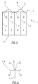
- the starting point is an electronic component designed as a stack 1.
- the stack 1 is formed from a plurality of material layers 2 reacting upon application of an electric field and a plurality of electrode layers 3, 4. Each of the material layers 2 is arranged between two of the electrode layers 3, 4.
- the electrode layers 3, 4 are guided on both sides to the respective edges of the stack 1.
- An electrical contacting takes place, for example, in interaction on opposite and geometrically non-contiguous stack circumferential regions 5, 6.
- the surfaces of the stack peripheral regions 5, 6 are generally ground to obtain planar surfaces for the further production steps.
- Such a stack 1 is in principle of the prior art known and used for example as a piezoelectric actuator for a piezoelectric injector for an internal combustion engine.
- an insulation structure 7 is applied to the stack circumferential region 5.
- the insulation structure 7 is structured such that the electrode layers 4 are exposed on the stack peripheral region 5.
- insulating walls 9 are applied to the electrode layers 3.
- their flanks extend obliquely in the direction of the component stack 1.
- the flanks could also be formed perpendicular to the plane of the stack perimeter region or curved, etc.
- an insulation structure 8 with insulating walls 10 is provided on the electrode layers 4 on the stack peripheral region 6.
- Flanks of the insulating walls 10 also extend only by way of example in the direction of the component stack 1, wherein the electrode layers 3 are exposed. It is obvious to a person skilled in the art that the flanks of the insulating walls 10 could also deviate from the shape shown.
- the generation of the isolation structures 7, 8 takes place, for example, by a subtractive method.
- a layer suitable for electrical insulation for example made of a polymer or a ceramic or a temperature-stable glass, is applied in a planar manner to the respective stack peripheral area 5, 6.
- a patterning process such as laser ablation or photopatterning
- every second of the electrode layers 3, 4 is opened on a respective stack perimeter area.
- the isolation structure can also be applied via a direct structuring method, for example by means of spraying or dispensing. If the material of the insulation structure is formed from a temperature-stable glass, it is expedient if this has a reduced silver migration. As a result, the insulating property of the glass is not adversely affected for a long period of time.
- the electrical contacting of the electrode layers 4 on the stack peripheral region 5 and the electrode layers 3 on the stack peripheral region 6 is realized by a contacting structure, which can be realized for example by means of a conductive adhesive.
- a conductive adhesive are in a non-conductive material, such. a resin of polyimide or epoxy, conductive metal particles introduced. Suitable materials are, in particular, gold, silver, palladium, platinum, copper or nickel and their alloys.
- the thickness of the contacting structure depends on the current carrying capacity of the contacting structure to be achieved.
- the contacting structures could also be formed from a metal or a metal alloy.
- a respective contacting structure 13, 14 thus assumes the electrical connection to the exposed electrode layers 3 and 4 and serves to conduct current with a predetermined current carrying capacity.
- the contacting structure 13, 14 thus forms respective outer electrodes.
- the electrode layers 4 are only a few microns, typically 1 to 4 microns, thick, especially when using a conductive adhesive as the material of the contacting structure there is a risk that some of the electrode layers or portions of electrode layers are not sufficiently electrically connected to the contacting structure. This results in a high contact resistance, so that locally excessive current densities and elevated temperatures can occur.
- the invention proposes to partially remove the material layers in such a way that the electrode layers are exposed near the surface before the contacting structure is produced by means of a material-removing method. This is for example in Fig. 2 represented, wherein the partial removal of the material of the material layers takes place here before applying the insulation structure.
- the removal of the material of the material layers can be done for example by means of grinding, brushing, blasting or by a laser.
- Will the stack perimeter areas 5, 6 (where in Fig. 2 only the stack perimeter area 5 is shown) is processed by means of sand blasting, the result, for example, between two adjacent electrode layers is a concave shape of the surfaces of the material layers 2 Fig. 2 Section shown here runs parallel to a longitudinal axis of the stack (which in Fig. 2 in sheet plane from left to right) and perpendicular through the stack perimeter area 5 (ie, in sheet plane from top to bottom).
- near-surface sections of the electrode layers 3, 4 are at least partially exposed at their opposite main surfaces 22, 23 in addition to their end face 21 adjoining the stack peripheral region 5, 6. This is increased and for only two adjacent material layers 2 in Fig. 4 shown.
- the depth T of material removal of the material of the material layers 2 is at most 10 .mu.m to 20 .mu.m, starting from the outermost end of an electrode layer 3, 4 to the lowest point of the machined material layer 2.
- the selected processing method is here in the area of the electrode layers under certain circumstances result in a lower material removal than, for example, in the middle between two electrode layers.
- only a few microns in the near-surface region of the electrode layers are freed from the material of the material layer 2.
- these exposed contact surfaces of the electrode layers are sufficient to provide a better electrical connection to the material of the contacting structure.
- Fig. 3 a section of a component stack 1 is shown, in which the production of the material removal 20 takes place only after the generation of the insulation structure 7.
- the exposure of the For the contacting structure required areas in the insulation 9 and the production of the material removal 20 can be done using the same processing method.
- the trenches can be produced in the isolation structure 7 with a laser. This can be further used to remove the material of the material layer 2 in the area between two walls 9, so that again the concave material erosion arise.
- the trenches in the insulation structure 7 and the production of the material erosions 20 in the material layers 2 can also be produced with different processing methods.
- the finished manufactured component stack has a planar surface.
- the proposed procedure is advantageous in particular in connection with the use of conductive adhesive as the material of the contacting structure, since after application of the material of the contacting structure, the metal particles contained in the conductive adhesive are randomly distributed. However, the larger the contact area available for the metal particles, the lower the risk that localized sites with high contact resistance will result.
Landscapes
- Engineering & Computer Science (AREA)
- Manufacturing & Machinery (AREA)
- Physics & Mathematics (AREA)
- Plasma & Fusion (AREA)
- Thermal Sciences (AREA)
- Mechanical Engineering (AREA)
- Fixed Capacitors And Capacitor Manufacturing Machines (AREA)
- Internal Circuitry In Semiconductor Integrated Circuit Devices (AREA)
- Manufacture Of Switches (AREA)
- Manufacturing Of Electrical Connectors (AREA)
- Coils Or Transformers For Communication (AREA)
Description
Die Erfindung betrifft ein Verfahren zum elektrischen Kontaktieren eines elektronischen Bauelements als Stapel, das aus einer Mehrzahl von auf Anlegen eines elektrischen Feldes reagierenden Werkstoffschichten und einer Anzahl von Elektrodenschichten gebildet ist, wobei jede Werkstoffschicht zwischen zwei der Elektrodenschichten angeordnet ist, gemäß dem Oberbegriff des Patentanspruches 1. Die Erfindung betrifft ferner ein als Stapel ausgebildetes elektronisches Bauelement der oben genannten Art gemäß dem Oberbegriff des Patentanspruches 9.The invention relates to a method for electrically contacting an electronic component as a stack, which is formed from a plurality of reacting on application of an electric field material layers and a number of electrode layers, each material layer is disposed between two of the electrode layers, according to the preamble of
Ein solches Bauelement aus übereinander und alternierend zueinander gestapelten Schichten von Werkstoffschicht und Elektrodenschicht wird allgemein als Stapel bezeichnet. Das heutzutage bekannteste elektronische Bauelement dieser Art ist ein allgemein als Piezoaktor bezeichneter Stapel, der als Betätigungselement in Einspritzventilen der verschiedensten Motortypen für Kraftfahrzeuge zur Anwendung kommt. Die Werkstoffschichten sind bei diesem Piezoaktor Keramikschichten.Such a component of layers of material layer and electrode layer, stacked one above the other and alternately with one another, is generally referred to as a stack. The most popular electronic component of this type today is a stack commonly referred to as a piezoactuator, which is used as an actuator in injection valves of a wide variety of engine types for motor vehicles. The material layers are ceramic layers in this piezoelectric actuator.
Üblicherweise weist ein solcher Stapel, in der Draufsicht betrachtet, einen rechteckigen oder quadratischen Querschnitt auf. Der Stapel wird an zwei sich gegenüberliegenden Umfangsseiten elektrisch kontaktiert. Um dies technologisch sorgfältig durchführen zu können, wurden die Elektrodenschichten in der Vergangenheit geometrisch so ausgelegt, dass sich nur jede zweite Elektrodenschicht seitlich bis zu einer der beiden Umfangsseiten erstreckt, während sich die jeweils anderen Elektrodenschichten nicht bis zu dieser Umfangsseite hin erstrecken. Entsprechendes gilt für die andere Umfangsseite des Stapels analog.Usually, such a stack, viewed in plan view, has a rectangular or square cross-section. The stack is electrically contacted on two opposite circumferential sides. In order to carry this out technologically carefully, the electrode layers were geometrically designed in the past so that only every second electrode layer extends laterally to one of the two circumferential sides, while the respective other electrode layers do not extend to this peripheral side. The same applies analogously to the other circumferential side of the stack.
Darüber hinaus sind sog. vollaktive Stapel bekannt, bei denen die Elektrodenschichten und die Werkstoffschichten die gleiche Fläche aufweisen, wodurch sich sämtliche Elektrodenschichten jeweils bis an die gegenüberliegenden Umfangsseiten erstrecken. Da sich sämtliche Elektrodenschichten des Bauelements bis zu den beiden gegenüberliegenden Umfangsseiten erstrecken, muss die Kontaktierung auf andere Weise erfolgen.In addition, so-called. Fully active stack are known in which the electrode layers and the material layers have the same area, whereby all the electrode layers each extend to the opposite peripheral sides. Since all the electrode layers of the component extend as far as the two opposite circumferential sides, the contacting must take place in other ways.
Aus der
Aus der
Allgemein sind aufgrund gegebener Anforderungen eine hohe Temperaturbeständigkeit des Aktors sowie eine hohe Dauerhaltbarkeit gefordert. Wesentlich hierfür ist eine gute Anbindung von Außenelektroden an die sehr dünnen Elektrodenschichten des Stapels. Ist die elektrische Anbindung der Außenelektroden an die Elektrodenschichten nicht niederohmig oder fehlerstellenbehaftet, kann es lokal zu überhöhten Stromdichten und damit erhöhten Temperaturen kommen, welche im schlechtesten Fall zu einer dauerhaften Dekontaktierung führen können. Diese Problematik ist insbesondere dann gegeben, wenn das Material der Außenelektroden, welche auf den gegenüberliegenden Umfangsseiten die Elektrodenschichten elektrisch kontaktieren, aus einem Leitkleber gebildet ist. Ein Leitkleber umfasst elektrisch leitende Partikel, beispielsweise aus Silber, Gold oder einem beliebigen anderen Metall oder einer Metalllegierung, welche in ein isolierendes Trägermaterial, z.B. ein Polyimidharz, ein Epoxidharz, usw., eingebettet sind.Generally, due to given requirements, a high temperature resistance of the actuator and a high durability are required. Essential for this is a good connection of external electrodes to the very thin electrode layers of the stack. If the electrical connection of the outer electrodes to the electrode layers is not low-resistance or faulty, locally excessive current densities and thus elevated temperatures can occur, which in the worst case can lead to permanent decontacting. This problem is especially given when the material of the outer electrodes, which on the opposite peripheral sides contacting the electrode layers electrically, is formed from a conductive adhesive. A conductive adhesive comprises electrically conductive particles, for example of silver, gold or any other metal or a metal alloy, which are embedded in an insulating support material, for example a polyimide resin, an epoxy resin, etc.
In
In
Es ist daher Aufgabe der vorliegenden Erfindung, ein Verfahren zum elektrischen Kontaktieren eines elektronischen Bauelements als Stapel sowie ein elektronisches Bauelement anzugeben, welche eine verbesserte Langzeit-Zuverlässigkeit des Stapels ermöglichen.It is therefore an object of the present invention to provide a method for electrically contacting an electronic component as a stack and an electronic component, which allow improved long-term reliability of the stack.
Diese Aufgaben werden gelöst durch ein Verfahren gemäß den Merkmalen des Patentanspruches 1 sowie ein als Stapel ausgebildetes elektronisches Bauelement gemäß den Merkmalen des Patentanspruchs 9. Vorteilhafte Ausgestaltungen ergeben sich jeweils aus den abhängigen Patentansprüchen.These objects are achieved by a method according to the features of
Die Erfindung schafft ein Verfahren zum elektrischen Kontaktieren eines elektronischen Bauelements als Stapel, das aus einer Mehrzahl von auf Anlegen eines elektrischen Feldes reagierenden Werkstoffschichten und einer Mehrzahl von Elektrodenschichten gebildet ist, wobei jede Werkstoffschicht zwischen zwei der Elektrodenschichten angeordnet ist. Auf zumindest einem Stapelumfangsbereich des Stapels wird eine Isolationsstruktur erzeugt, so dass jede zweite Elektrodenschicht des zumindest einen Stapelumfangsbereichs zur elektrischen Kontaktierung freigelegt ist.The invention provides a method for electrically contacting an electronic component as a stack, which is formed from a plurality of reacting on application of an electric field material layers and a plurality of electrode layers, wherein each material layer between two of the electrode layers is arranged. An insulation structure is produced on at least one stack peripheral region of the stack, so that every second electrode layer of the at least one stack peripheral region is exposed for electrical contacting.
Bevorzugt wird dabei jede zweite, zu den frei gelegten Elektrodenschichten vorzugsweise alternierend angeordnete Elektrodenschicht zumindest teilweise von der Isolationsstruktur bedeckt.Preference is given here every second, preferably arranged alternately to the exposed electrode layers Electrode layer at least partially covered by the insulation structure.
Das Erzeugen der Isolationsstruktur und Freilegen jeder zweiten Elektrodenschicht von der Isolationsstruktur kann beispielsweise erfolgen, indem zunächst eine Isolationsschicht auf den Stapelumfangsbereich aufgetragen wird, von welcher anschließend zum Freilegen jeder zweiten Elektrodenschicht wieder Material entfernt wird. Alternativ kann die Isolationsstruktur auch über ein Direktstrukturierungsverfahren, z.B. mittels Sprühen oder Dispensen, aufgebracht werden, so dass jede zweite Elektrodenschicht frei bleibt.The generation of the insulation structure and the exposure of each second electrode layer from the insulation structure can take place, for example, by first applying an insulation layer to the insulation layer Stacking peripheral region is applied, from which subsequently to expose every second electrode layer material is removed again. Alternatively, the insulation structure can also be applied via a direct structuring method, for example by means of spraying or dispensing, so that every second electrode layer remains free.
Auf den zumindest einen, mit der Isolationsstruktur versehenen Stapelumfangsbereich wird dann eine Kontaktierungsstruktur aufgebracht. Vor dem Schritt des Erzeugens der Kontaktierungsstruktur wird mittels eines materialabtragenden Verfahrens lediglich das Material der Werkstoffschichten ohne Abtrag des Materials der Elektrodenschichten partiell derart abgetragen, dass die Elektrodenschichten oberflächennah freigelegt werden.A contacting structure is then applied to the at least one stack peripheral region provided with the insulation structure. Before the step of producing the contacting structure, only the material of the material layers without removal of the material of the electrode layers is partially removed by means of a material-removing method such that the electrode layers are exposed near the surface.
Vorzugsweise wird durch das partielle Abtragen der Werkstoffschichten zumindest jede zweite Elektrodenschicht oberflächennah freigelegt, insbesondere jede von der Isolationsstruktur freigelegte Elektrodenschicht.Preferably, at least every second electrode layer is exposed near the surface as a result of the partial removal of the material layers, in particular each electrode layer exposed by the insulation structure.
Der Vorteil des erfindungsgemäßen Verfahrens besteht darin, dass durch das oberflächennahe Freilegen der Elektrodenschichten eine vergrößerte Fläche zur elektrischen Kontaktierung der Elektrodenschichten zur Verfügung steht. Hierdurch ist eine bessere elektrische Anbindung der Elektrodenschichten an die Kontaktierungsstruktur möglich. Die Gefahr von lokalen überhöhten Stromdichten und damit erhöhten Temperaturen kann hierdurch verringert werden. Im Ergebnis wird hierdurch die Langzeit-Zuverlässigkeit des hergestellten Stapels verbessert.The advantage of the method according to the invention is that an enlarged surface for electrically contacting the electrode layers is available due to the exposure of the electrode layers close to the surface. As a result, a better electrical connection of the electrode layers to the contacting structure is possible. The risk of local excessive current densities and thus increased temperatures can be reduced thereby. As a result, the long-term reliability of the manufactured stack is improved.
In einer zweckmäßigen Weiterbildung des erfindungsgemäßen Verfahrens erfolgt das Abtragen des Materials der Werkstoffschichten derart, dass oberflächennahe Abschnitte der Elektrodenschichten zusätzlich zu ihrer an den Stapelumfangsbereich grenzenden Stirnseite zumindest teilweise an ihren Hauptflächen freigelegt werden. Die elektrische Kontaktierung kann damit nicht nur an den Stirnflächen der Elektrodenschichten erfolgen, welche lediglich jeweils wenige Mikrometer breit sind. Stattdessen kann zusätzlich ein Kontaktierungsbereich an den jeweiligen Hauptflächen geschaffen werden. Die Größe des Kontaktierungsbereichs hängt dabei im Wesentlichen von dem gewählten materialabtragenden Verfahren und der Dauer der Materialabtragung ab.In an expedient development of the method according to the invention, the removal of the material of the material layers takes place in such a way that near-surface portions of the electrode layers are at least partially exposed on their main surfaces in addition to their end face adjoining the stack peripheral region. The electrical contacting can thus take place not only on the end faces of the electrode layers, which are only a few microns wide. Instead, an additional contact area to the respective major surfaces are created. The size of the contacting region depends essentially on the chosen material-removing process and the duration of material removal.
Es sollte lediglich so viel Material der Werkstoffschichten abgetragen werden, dass eine erhöhte Kontaktfläche an den Elektrodenschichten geschaffen ist. Gleichzeitig darf die Stabilität der dünnen Elektrodenschichten durch das Abtragen der Materialschichten jedoch nicht geschwächt werden. Es ist ausreichend, wenn - ausgehend von einer durch die Stapelumfangsbereiche gebildeten Oberfläche - das Material der Werkstoffschichten wenige Mikrometer tief abgetragen wird. Insbesondere sollte das Abtragen des Materials der Werkstoffschichten eine Tiefe von 10 µm bis 20 µm nicht übersteigen. Bei größeren Tiefen besteht die Gefahr, dass die Elektrodenschichten und das Material der Werkstoffschichten, welches an die Elektroden grenzt, im weiteren Prozess der Weiterverarbeitung beschädigt werden könnten.It should only be removed so much material of the material layers that an increased contact surface is created at the electrode layers. At the same time, however, the stability of the thin electrode layers due to the removal of the material layers must not be weakened. It is sufficient if - starting from a surface formed by the stack peripheral areas - the material of the material layers is removed a few microns deep. In particular, the removal of the material of the material layers should not exceed a depth of 10 microns to 20 microns. At greater depths there is a risk that the electrode layers and the material of the material layers, which adjoins the electrodes, could be damaged in the further process of further processing.
In einer weiteren zweckmäßigen Ausgestaltung erfolgt das partielle, oberflächennahe Abtragen des Materials der Werkstoffschichten vor dem Schritt des Erzeugens der Isolationsstruktur. Hierzu kann beispielsweise ein jeweiliger Stapelumfangsbereich (auf die die Außenelektroden aufgebracht werden) vor dem Erzeugen der Isolationsstruktur plan geschliffen werden, so dass die Elektrodenschichten an den Oberflächen der jeweiligen Stapelumfangsbereiche zunächst bündig mit den Werkstoffschichten abschließen. Anschließend erfolgt das oberflächennahe partielle Abtragen des Materials der Werkstoffschichten, um die Elektrodenschichten ungefähr gleichförmig oberflächennah freizulegen.In a further expedient embodiment, the partial, near-surface removal of the material of the material layers takes place before the step of generating the insulation structure. For this purpose, for example, a respective stack perimeter area (to which the outer electrodes are applied) can be ground flat prior to the production of the insulation structure, so that the electrode layers initially terminate flush with the material layers on the surfaces of the respective stack perimeter areas. Subsequently, the near-surface partial removal of the material of the material layers takes place in order to expose the electrode layers approximately uniformly close to the surface.
Alternativ kann auch vorgesehen sein, dass das partielle, oberflächennahe Abtragen des Materials der Werkstoffschichten nach dem Schritt des Erzeugens der Isolationsstruktur erfolgt. Insbesondere können das Freilegen jeder zweiten Elektrodenschicht und das Abtragen des Materials der Werkstoffschichten durch das gleiche Bearbeitungsverfahren erfolgen. Ein Vorteil dieser Vorgehensweise besteht darin, dass keine zusätzlichen Werkzeuge oder Bearbeitungsschritte im Rahmen der Herstellung des Bauelementstapels bereitgestellt werden müssen. Das gleichzeitige Freilegen jeder zweiten Elektrodenschicht des zumindest einen Stapelumfangsbereichs zur elektrischen Kontaktierung und das Abtragen des Materials der Werkstoffschichten in den freigelegten Bereichen kann beispielsweise unter Verwendung eines Lasers geschehen.Alternatively it can also be provided that the partial, near-surface removal of the material of the material layers takes place after the step of generating the insulation structure. In particular, the exposure of each second electrode layer and the removal of the material of the material layers done by the same processing method. An advantage of this procedure is that no additional tools or processing steps must be provided in the context of the production of the component stack. The simultaneous exposure of each second electrode layer of the at least one stack peripheral region for electrical contacting and the removal of the material of the material layers in the exposed regions can be done, for example, using a laser.
Das partielle, oberflächennahe Abtragen des Materials der Werkstoffschichten kann beispielsweise mittels Schleifen, Bürsten, Strahlen oder den Laser erfolgen. Das Strahlen kann beispielsweise mittels in einen Trägerstrom eingebrachte Partikel (z.B. Sand) erfolgen. Durch die genannten Bearbeitungsverfahren kann sichergestellt werden, dass lediglich das Material der Werkstoffschichten, jedoch nicht das Material der Elektrodenschichten während des Bearbeitungsvorganges abgetragen wird. Ebenso sind diese Verfahren geeignet, das Material der auf die Stapelumfangsbereiche aufgebrachten Isolationsschicht zum Freilegen jeder zweiten Elektrodenschicht zu entfernen.The partial, near-surface removal of the material of the material layers can be done for example by means of grinding, brushing, blasting or laser. The blasting may, for example, be by means of particles introduced into a carrier stream (e.g., sand). By means of the mentioned processing methods, it can be ensured that only the material of the material layers, but not the material of the electrode layers, is removed during the machining process. Likewise, these methods are suitable for removing the material of the insulating layer applied to the stack circumferential areas to expose every second electrode layer.
In einer weiteren Ausgestaltung wird nach dem Schritt des Erzeugens der Isolationsstruktur und dem gegebenenfalls darauffolgenden Schritt des partiellen Abtragens des Materials der Werkstoffschicht eine dünne Metallschicht, insbesondere durch Sputtern, auf den Stapelumfangsbereich aufgebracht, auf welche in einem nachfolgenden Schritt die Kontaktierungsstruktur auf die dünne Metallschicht aufgebracht wird. Die dünne Metallschicht ermöglicht eine zuverlässigere und fehlstellenfreie Kontaktierung der Elektrodenschichten des Stapels. Wird die Kontaktierungsstruktur, wie dies bevorzugt ist, mittels eines Leitklebers realisiert, so können die in dem Leitkleber enthaltenen Metallpartikel die dünne Metallschicht auch im Bereich der Isolationsstruktur elektrisch kontaktieren und tragen damit zusätzlich zu einer Stromleitung bei. Auch hierdurch lässt sich die Zuverlässigkeit des elektronischen Bauelements erhöhen.In a further embodiment, after the step of generating the insulation structure and the optionally subsequent step of partially removing the material of the material layer, a thin metal layer, in particular by sputtering, is applied to the stack peripheral region, onto which the contacting structure is applied to the thin metal layer in a subsequent step becomes. The thin metal layer allows a more reliable and defect-free contacting of the electrode layers of the stack. If the contacting structure, as is preferred, realized by means of a conductive adhesive, the metal particles contained in the conductive adhesive can electrically contact the thin metal layer in the region of the insulation structure and thus contribute in addition to a power line. Also by this the reliability of the electronic component can be increased.
Die Erfindung schafft ferner ein als Stapel ausgebildetes elektronisches Bauelement. Dieses umfasst eine Mehrzahl von Elektrodenschichten und eine Mehrzahl von auf Anlegen eines elektrischen Feldes reagierenden Werkstoffschichten, wobei jede Werkstoffschicht zwischen zwei Elektrodenschichten angeordnet ist. Ferner ist eine Isolationsstruktur vorgesehen, die auf zumindest einem Stapelumfangsbereich des Stapels aufgebracht ist, wobei die Isolationsstruktur derart ausgebildet ist, dass jede zweite Elektrodenschicht eines Stapelumfangsbereichs zur elektrischen Kontaktierung freigelegt ist. Eine Kontaktierungsstruktur ist auf zumindest einen, mit der Isolationsstruktur versehenen Stapelumfangsbereich aufgebracht. Das als Stapel ausgebildete elektronische Bauelement zeichnet sich dadurch aus, dass die Werkstoffschichten in einem Schnitt, der parallel zu einer Längsachse des Stapels und senkrecht durch einen der Stapelumfangsbereiche verläuft, in einem oberflächennahen Bereich, der an die Elektrodenschichten angrenzt, zumindest teilweise derart abgetragen sind, dass die Elektrodenschichten sowohl an ihrer an den Stapelumfangsbereich grenzenden Stirnseite als auch zumindest teilweise an ihren sich gegenüberliegenden Hauptflächen freigelegt sind, und durch Material der Isolationsstruktur oder der Kontaktierungsstruktur ersetzt sind.The invention further provides an electronic component designed as a stack. This comprises a plurality of electrode layers and a plurality of material layers reacting upon application of an electric field, wherein each material layer is arranged between two electrode layers. Furthermore, an insulation structure is provided, which is applied to at least one stack peripheral region of the stack, wherein the insulation structure is formed such that every second electrode layer of a stack peripheral region is exposed for electrical contacting. A contacting structure is applied to at least one stack peripheral region provided with the insulation structure. The stacked electronic component is characterized in that the material layers are at least partially removed in a section that is parallel to a longitudinal axis of the stack and perpendicularly through one of the stack peripheral regions in a region close to the surface that adjoins the electrode layers. in that the electrode layers are exposed both at their end face adjoining the stack peripheral region and at least partially at their opposing main surfaces, and are replaced by material of the insulation structure or the contacting structure.
Insbesondere können vorzugsweise die Werkstoffschichten in einem oberflächennahen Bereich, der an die freigelegten Elektrodenschichten angrenzt, zumindest teilweise abgetragen und durch Material der Kontaktierungsstruktur ersetzt sein. Somit ist vorteilhaft jede zweite Elektrodenschicht mit der Kontaktierungsstruktur verbunden.In particular, the material layers in a region close to the surface, which adjoins the exposed electrode layers, may preferably be at least partially removed and replaced by material of the contacting structure. Thus, each second electrode layer is advantageously connected to the contacting structure.
Unter dem oberflächennahen Bereich des Stapels ist hierbei eine Ebene bzw. Oberfläche des Stapelumfangsbereichs zu verstehen, wenn die Isolationsstruktur und die Kontaktierungsstruktur noch nicht auf den Stapelumfangsbereich aufgebracht sind. Nach dem Aufbringen grenzen die Isolationsstruktur bzw. die Kontaktierungsstruktur an den oberflächennahen Bereich der Werkstoffschichten.In this case, the near-surface region of the stack is to be understood as meaning a plane or surface of the stack circumferential region if the insulation structure and the contacting structure not yet applied to the stack perimeter area. After application, the insulation structure or the contacting structure adjoin the area near the surface of the material layers.
Der erfindungsgemäß ausgebildete Stapel weist die gleichen Vorteile auf, wie diese vorstehend in Verbindung mit dem erfindungsgemäßen Verfahren erläutert wurden.The stack formed according to the invention has the same advantages as have been explained above in connection with the method according to the invention.
Die Oberflächenform der durch Materialabtragung bearbeiteten Werkstoffschichten ist so ausgebildet, dass die Werkstoffschichten in einer Schnittansicht durch den Schnitt zwischen zwei benachbarten Elektrodenschichten eine konkave Gestalt aufweisen. Die konkave Gestalt ergibt sich aus dem für die Bearbeitung gewählten materialabtragenden Verfahren. Insbesondere sind die Werkstoffschichten gegenüber dem Stapelumfangsbereich bereichsweise um höchstens 10 µm bis 20 µm reduziert. Diese geringe Materialabtragung ermöglicht einerseits eine verbesserte Kontaktierung der freigelegten Abschnitte der Elektrodenschichten. Andererseits ist die Materialreduzierung derart gering, dass die Weiterverarbeitung des derart vorbereiteten Stapels keine Abänderung der Verfahrensschritte zum Aufbringen der Isolationsstruktur und der Kontaktierungsstruktur erfordert. Insbesondere kann aufgrund der geringen Materialabtragung auch sichergestellt werden, dass die Oberflächen eines fertiggestellten Stapels eben sind.The surface shape of the material layers processed by material removal is designed so that the material layers have a concave shape in a sectional view through the intersection between two adjacent electrode layers. The concave shape results from the material-removing process chosen for the machining. In particular, the material layers are reduced in regions relative to the stack peripheral region by at most 10 μm to 20 μm. This low material removal on the one hand enables improved contacting of the exposed sections of the electrode layers. On the other hand, the material reduction is so low that the further processing of the thus prepared stack requires no modification of the method steps for applying the insulation structure and the contacting structure. In particular, due to the low material removal, it can also be ensured that the surfaces of a finished stack are flat.
Zweckmäßigerweise umfasst das Material der Kontaktierungsstruktur einen Leitkleber mit einem Träger aus einem nicht-leitenden Material, insbesondere Polyimid, und darin eingebetteten Metallpartikeln. Ein Vorteil der Verwendung eines Leitklebers als Material für die Kontaktierungsstruktur besteht darin, dass das nichtleitende Trägermaterial des Leitklebers ähnliche Eigenschaften aufweist, wie das zur Erzeugung der Isolationsstruktur eingesetzte Material. Hierdurch kann eine hohe Langzeit-Zuverlässigkeit des Stapels begünstigt werden, da hohe Temperaturen nicht zu unterschiedlichen Ausdehnungen der Isolations- und der Kontaktierungsstruktur führen. Weiterhin ist durch die vergrößerte Kontaktierungsfläche der Elektrodenschichten die Gefahr fehlstellenbehafteter Kontaktstellen verringert.Conveniently, the material of the contacting structure comprises a conductive adhesive with a support of a non-conductive material, in particular polyimide, and embedded therein metal particles. An advantage of using a conductive adhesive as the material for the contacting structure is that the non-conductive carrier material of the conductive adhesive has similar properties as the material used to produce the insulating structure. In this way, a high long-term reliability of the stack can be promoted, since high temperatures do not lead to different expansions of the insulation and the contacting structure. Furthermore, the risk of faulty contact points is reduced by the increased contact surface of the electrode layers.
Die Erfindung wird nachfolgend näher anhand von Ausführungsbeispielen in der Zeichnung beschrieben. Es zeigen:
- Fig. 1
- eine schematische Querschnittsdarstellung eines bekannten Bauelements, auf dessen Stapel aus Werkstoffschichten und Elektrodenschichten eine Isolationsstruktur und eine Kontaktierungsstruktur aufgebracht ist,
- Fig. 2
- eine schematische Querschnittsdarstellung eines Teils einer ersten Ausführungsform eines erfindungsgemäßen Bauelementstapels, bei dem die Werkstoffschichten partiell abgetragen sind,
- Fig. 3
- eine schematische Querschnittsdarstellung eines Teils einer zweiten Ausführungsform eines erfindungsgemäßen Bauelementstapels, bei dem die Werkstoffschichten in einer alternativen Ausgestaltung partiell abgetragen sind, und
- Fig. 4
- eine vergrößerte Darstellung der Materialabtragung im Bereich einer Elektrodenschicht eines Bauelementstapels.
- Fig. 1
- 2 a schematic cross-sectional view of a known component, on the stack of material layers and electrode layers of which an insulation structure and a contacting structure are applied,
- Fig. 2
- FIG. 2 a schematic cross-sectional representation of a part of a first embodiment of a component stack according to the invention, in which the material layers have been partially removed, FIG.
- Fig. 3
- a schematic cross-sectional view of a portion of a second embodiment of a component stack according to the invention, in which the material layers are partially removed in an alternative embodiment, and
- Fig. 4
- an enlarged view of the material removal in the region of an electrode layer of a component stack.
Ausgangspunkt ist ein als Stapel 1 ausgebildetes elektronisches Bauelement. Der Stapel 1 ist aus einer Mehrzahl von auf Anlegen eines elektrischen Feldes reagierenden Werkstoffschichten 2 und einer Mehrzahl von Elektrodenschichten 3, 4 gebildet. Jede der Werkstoffschichten 2 ist zwischen zwei der Elektrodenschichten 3, 4 angeordnet. Die Elektrodenschichten 3, 4 sind beidseitig bis an die jeweiligen Ränder des Stapels 1 geführt. Eine elektrische Kontaktierung erfolgt beispielhaft im Zusammenspiel auf gegenüberliegenden und geometrisch nicht zusammenhängenden Stapelumfangsbereichen 5, 6. Die Oberflächen der Stapelumfangsbereiche 5, 6, sind in der Regel geschliffen, um ebene Oberflächen für die weiteren Herstellungsschritte zu erhalten. Ein derartiger Stapel 1 ist aus dem Stand der Technik prinzipiell bekannt und dient beispielsweise als Piezoaktor für einen Piezoinjektor für einen Verbrennungsmotor.The starting point is an electronic component designed as a
Wie der schematischen Querschnittsdarstellung der
In entsprechender Weise ist auf dem Stapelumfangsbereich 6 eine Isolationsstruktur 8 mit Isolationswällen 10 auf den Elektrodenschichten 4 vorgesehen. Flanken der Isolationswälle 10 erstrecken sich ebenfalls lediglich beispielhaft in Richtung des Bauelementstapels 1, wobei die Elektrodenschichten 3 freigelegt sind. Es versteht sich für einen Fachmann, dass auch die Flanken der Isolationswälle 10 von der gezeigten Form abweichen könnten.In a corresponding manner, an
Die Erzeugung der Isolationsstrukturen 7, 8 erfolgt z.B. durch ein subtraktives Verfahren. Hierbei wird zunächst eine zur elektrischen Isolation geeignete Schicht, z.B. aus einem Polymer oder einer Keramik oder einem temperaturstabilen Glas, flächig auf den jeweiligen Stapelumfangsbereich 5, 6 aufgebracht. Über ein Strukturierungsverfahren, wie z.B. Laserablation oder Fotostrukturierung, wird jede zweite der Elektrodenschichten 3, 4 auf einem jeweiligen Stapelumfangsbereich geöffnet. Wahlweise kann die Isolationsstruktur auch über ein Direktstrukturierungsverfahren, z.B. mittels Sprühen oder Dispensen, aufgebracht werden. Sofern das Material der Isolationsstruktur aus einem temperaturstabilen Glas gebildet wird, ist es zweckmäßig, wenn dieses eine verringerte Silbermigration aufweist. Hierdurch wird die Isolationseigenschaft des Glases für einen langen Zeitraum nicht negativ beeinflusst.The generation of the
Die elektrische Kontaktierung der Elektrodenschichten 4 auf dem Stapelumfangsbereich 5 bzw. der Elektrodenschichten 3 auf dem Stapelumfangsbereich 6 wird durch eine Kontaktierungsstruktur realisiert, welche beispielsweise mittels eines Leitklebers realisiert werden kann. Bei einem Leitkleber sind in einem nicht-leitenden Material, wie z.B. einem Harz aus Polyimid oder Epoxyd, leitende Metallpartikel, eingebracht. Als Materialien kommen insbesondere Gold, Silber, Palladium, Platin, Kupfer oder Nickel sowie deren Legierungen in Betracht. Die Dicke der Kontaktierungsstruktur hängt von der zu erzielenden Stromtragfähigkeit der Kontaktierungsstruktur ab. Ebenso könnten die Kontaktierungsstrukturen auch aus einem Metall oder einer Metalllegierung gebildet sein.The electrical contacting of the electrode layers 4 on the stack
Eine jeweilige Kontaktierungsstruktur 13, 14 übernimmt somit die elektrische Anbindung an die freigelegten Elektrodenschichten 3 bzw. 4 und dient zur Stromführung mit einer vorgegebenen Stromtragfähigkeit. Die Kontaktierungsstruktur 13, 14 bildet somit jeweilige Außenelektroden.A respective contacting
Da die Elektrodenschichten 4 nur wenige Mikrometer, typischerweise 1 bis 4 µm, dick sind, ist insbesondere bei der Verwendung eines Leitklebers als Material der Kontaktierungsstruktur die Gefahr gegeben, dass einzelne der Elektrodenschichten oder Abschnitte von Elektrodenschichten nicht ausreichend elektrisch an die Kontaktierungsstruktur angebunden sind. Hierdurch entsteht ein hoher Kontaktwiderstand, so dass es zu lokal überhöhten Stromdichten und erhöhten Temperaturen kommen kann.Since the electrode layers 4 are only a few microns, typically 1 to 4 microns, thick, especially when using a conductive adhesive as the material of the contacting structure there is a risk that some of the electrode layers or portions of electrode layers are not sufficiently electrically connected to the contacting structure. This results in a high contact resistance, so that locally excessive current densities and elevated temperatures can occur.
Um die Anbindung des Materials der Kontaktierungsstruktur an die Elektrodenschichten zu verbessern, schlägt die Erfindung vor, vor dem Erzeugen der Kontaktierungsstruktur mittels eines materialabtragenden Verfahrens die Werkstoffschichten partiell derart abzutragen, dass die Elektrodenschichten oberflächennah freigelegt sind. Dies ist beispielsweise in
Das Abtragen des Materials der Werkstoffschichten kann beispielsweise mittels Schleifen, Bürsten, Strahlen oder durch einen Laser erfolgen. Werden die Stapelumfangsbereiche 5, 6 (wobei in
Die Tiefe T des Materialabtrags des Materials der Werkstoffschichten 2 beträgt höchstens 10 µm bis 20 µm, ausgehend vom äußersten Ende einer Elektrodenschicht 3, 4 bis zum tiefsten Punkt der bearbeiteten Werkstoffschicht 2. Abhängig von dem gewählten Bearbeitungsverfahren wird sich hier im Bereich der Elektrodenschichten unter Umständen ein geringerer Materialabtrag als beispielsweise in der Mitte zwischen zwei Elektrodenschichten ergeben. Hierdurch bedingt werden lediglich einige Mikrometer im oberflächennahen Bereich der Elektrodenschichten vom Material der Werkstoffschicht 2 befreit. Diese freigelegten Kontaktflächen der Elektrodenschichten reichen jedoch aus, eine bessere elektrische Anbindung an das Material der Kontaktierungsstruktur bereitzustellen.The depth T of material removal of the material of the material layers 2 is at most 10 .mu.m to 20 .mu.m, starting from the outermost end of an
In
In einer alternativen Ausgestaltung kann das Erzeugen der Gräben in der Isolationsstruktur 7 und das Erzeugen der Materialabtragungen 20 in den Werkstoffschichten 2 auch mit unterschiedlichen Bearbeitungsverfahren erfolgen.In an alternative embodiment, the trenches in the
Um die elektrische Anbindung der Kontaktierungsstruktur 13, 14 an die Elektrodenschichten 3, 4 weiter zu verbessern, kann ferner vorgesehen sein, auf die in den
Aufgrund der geringen Tiefe der Materialabtragung 20 in den Werkstoffschichten ist nach dem Erzeugen der Isolationsstruktur und der Kontaktierungsstruktur dennoch sichergestellt, dass der fertig hergestellte Bauelementstapel eine ebene Oberfläche aufweist.Due to the shallow depth of the
Das vorgeschlagene Vorgehen ist insbesondere in Verbindung mit der Verwendung von Leitkleber als Material der Kontaktierungsstruktur von Vorteil, da nach dem Aufbringen des Materials der Kontaktierungsstruktur sich die in dem Leitkleber enthaltenen Metallpartikel zufällig verteilen. Je größer jedoch die zur Verfügung stehende Kontaktfläche für die Metallpartikel ist, desto geringer ist die Gefahr, dass lokale Stellen mit hohem Kontaktwiderstand entstehen. The proposed procedure is advantageous in particular in connection with the use of conductive adhesive as the material of the contacting structure, since after application of the material of the contacting structure, the metal particles contained in the conductive adhesive are randomly distributed. However, the larger the contact area available for the metal particles, the lower the risk that localized sites with high contact resistance will result.
Claims (11)
- Method for making electrical contact with an electronic component in the form of a stack (1) which is formed from a plurality of material layers (2) that react upon application of an electric field, and a plurality of electrode layers (3, 4), wherein each material layer (2) is arranged between two of the electrode layers (3, 4), in which- an insulation structure (7, 8) is produced on at least one stack circumferential region (5, 6) of the stack (1), with the result that every second electrode layer (3, 4) of the at least one stack circumferential region (5, 6) is exposed for electrical contact to be made;- a contact-making structure (13, 14) is applied to the at least one stack circumferential region (5, 6) that is provided with the insulation structure (7, 8);wherein- before the step of producing the contact-making structure (13, 14), only the material of the material layers (2) is partially removed, without removal of the material of the electrode layers, by means of a material-removing method in such a way that at least every second electrode layer (3, 4) is exposed close to the surface and that the material layers (2) have a concave form, in a section which extends parallel to a longitudinal axis of the stack (1) and perpendicularly through one of the stack circumferential regions (5, 6), between two adjacent electrode layers (3, 4), wherein a lesser material removal (20) of the material of the material layers (2) results in the region of the electrode layers (3, 4) than in the middle between the two electrode layers (3, 4).
- Method according to Claim 1,
characterized in that
the removal of the material of the material layers (2) takes place such that sections, close to the surface, of the electrode layers (3, 4) are at least partially exposed at their main surfaces in addition to their end sides adjoining the stack circumferential region (5, 6). - Method according to Claim 1 or 2,
characterized in that
the partial removal, close to the surface, of the material of the material layers (2) takes place before the step of producing the insulation structure. - Method according to Claim 1 or 2,
characterized in that
the partial removal, close to the surface, of the material of the material layers (2) takes place after the step of producing the insulation structure. - Method according to Claim 4,
characterized in that
at the same time as the exposure of every second electrode layer (3, 4) of the at least one stack circumferential region (5, 6) for making electrical contact, the removal of the material of the material layers (2) in the exposed regions takes place. - Method according to Claim 4 or 5,
characterized in that
the exposure of every second electrode layer (3, 4) and the removal of the material of the material layers (2) take place by way of the same machining method. - Method according to one of the preceding claims,
characterized in that
the partial removal, close to the surface, of the material of the material layers (2) takes place by means of grinding, brushing, blasting or by way of a laser. - Method according to one of the preceding claims,
characterized in that
after the step of producing the insulation structure (7, 8) and the optionally following step of partially removing the material of the material layers (2), a thin metal layer is applied to the stack circumferential region (7, 8), in particular by sputtering, the contact-making structure (13, 14) being applied to said thin metal layer in a subsequent step. - Electronic component in the form of a stack (1), comprising:- a plurality of electrode layers (3, 4);- a plurality of material layers (2) that react upon application of an electric field, wherein each material layer (2) is arranged between two of the electrode layers (3, 4) ;- an insulation structure (7, 8) which has been applied to at least one stack circumferential region (5, 6) of the stack (1), wherein the insulation layer (7) has been formed such that every second electrode layer (3, 4) of a stack circumferential region (5, 6) is exposed for electrical contact to be made;- a contact-making structure (13, 14) applied to the at least one stack circumferential region (5, 6) provided with the insulation structure (7, 8);wherein- the material layers (2) have been at least partially removed in such a way that the electrode layers are exposed both at their end sides adjoining the stack circumferential region and at least partially at their opposite main surfaces, and replaced by material of the insulation structure (7, 8) or of the contact-making structure (13, 14) in a section which extends parallel to a longitudinal axis of the stack (1) and perpendicularly through one of the stack circumferential regions (5, 6), at least in a region, close to the surface, which adjoins the exposed electrode layers (3, 4),- the material layers (2) have a concave form in the section which extends parallel to a longitudinal axis of the stack (1) and perpendicularly through one of the stack circumferential regions (5, 6) between two adjacent electrode layers (3, 4), characterized in that there is a lesser material removal (20) of the material of the material layers (2) in the region of the electrode layers (3, 4) than in the middle between the two electrode layers (3, 4).
- Stack according to Claim 9,
characterized in that
the material layers (2) have been reduced regionally by at most 10 µm to 20 µm with respect to the stack circumferential region (5, 6). - Stack according to either of Claims 9 and 10,
characterized in that
the material of the contact-making structure (13, 14) comprises a conductive adhesive having a backing made of a nonconductive material,
in particular polyimide, and metal particles embedded therein.
Applications Claiming Priority (2)
| Application Number | Priority Date | Filing Date | Title |
|---|---|---|---|
| DE102012207598A DE102012207598A1 (en) | 2012-05-08 | 2012-05-08 | Method for electrically contacting an electronic component as a stack and electronic component with a contacting structure |
| PCT/EP2013/059562 WO2013167643A2 (en) | 2012-05-08 | 2013-05-08 | Method for making electrical contact with an electronic component in the form of a stack, and electronic component having a contact-making structure |
Publications (2)
| Publication Number | Publication Date |
|---|---|
| EP2777083A2 EP2777083A2 (en) | 2014-09-17 |
| EP2777083B1 true EP2777083B1 (en) | 2016-01-20 |
Family
ID=48325731
Family Applications (1)
| Application Number | Title | Priority Date | Filing Date |
|---|---|---|---|
| EP13720962.3A Active EP2777083B1 (en) | 2012-05-08 | 2013-05-08 | Method for making electrical contact with an electronic component in the form of a stack, and electronic component having a contact-making structure |
Country Status (5)
| Country | Link |
|---|---|
| US (1) | US9691965B2 (en) |
| EP (1) | EP2777083B1 (en) |
| JP (1) | JP5875702B2 (en) |
| DE (1) | DE102012207598A1 (en) |
| WO (1) | WO2013167643A2 (en) |
Families Citing this family (7)
| Publication number | Priority date | Publication date | Assignee | Title |
|---|---|---|---|---|
| JPWO2013157293A1 (en) * | 2012-04-19 | 2015-12-21 | 日本碍子株式会社 | Film-type piezoelectric / electrostrictive element |
| DE102012207598A1 (en) * | 2012-05-08 | 2013-11-14 | Continental Automotive Gmbh | Method for electrically contacting an electronic component as a stack and electronic component with a contacting structure |
| DE102015214778A1 (en) * | 2015-08-03 | 2017-02-09 | Continental Automotive Gmbh | Manufacturing method for manufacturing an electromechanical actuator and electromechanical actuator |
| DE102015215204A1 (en) * | 2015-08-10 | 2017-02-16 | Continental Automotive Gmbh | Manufacturing method for manufacturing an electromechanical actuator and electromechanical actuator. |
| DE102015217334B3 (en) * | 2015-09-10 | 2016-12-01 | Continental Automotive Gmbh | Method for producing a stacked multilayer actuator |
| DE102016202839A1 (en) * | 2016-02-24 | 2017-03-09 | Continental Automotive Gmbh | Piezoelectric layer stack and method for producing a piezoelectric layer stack |
| CN112518434B (en) * | 2020-10-20 | 2021-10-01 | 陕西斯瑞新材料股份有限公司 | Metal auxiliary machining process for removing burrs of CuCr contact by physical method |
Citations (1)
| Publication number | Priority date | Publication date | Assignee | Title |
|---|---|---|---|---|
| JP2005079313A (en) * | 2003-08-29 | 2005-03-24 | Denso Corp | Manufacturing method of multilayer piezoelectric element |
Family Cites Families (21)
| Publication number | Priority date | Publication date | Assignee | Title |
|---|---|---|---|---|
| JPS62239588A (en) * | 1986-04-10 | 1987-10-20 | Nagai Denshi Kogyo Kyodo Kumiai | Manufacture of piezoelectric element of laminated ceramics |
| WO1992005593A1 (en) * | 1990-09-13 | 1992-04-02 | Hitachi Metals, Ltd. | Method for manufacturing electrostrictive effect element |
| JPH053352A (en) * | 1991-06-04 | 1993-01-08 | Alps Electric Co Ltd | Laminated piezoelectric actuator and method for manufacturing the same |
| JPH0529680A (en) * | 1991-07-25 | 1993-02-05 | Hitachi Metals Ltd | Laminated displacement element and manufacture thereof |
| US5406164A (en) * | 1993-06-10 | 1995-04-11 | Brother Kogyo Kabushiki Kaisha | Multilayer piezoelectric element |
| JPH0774410A (en) * | 1994-09-06 | 1995-03-17 | Ngk Spark Plug Co Ltd | Method for manufacturing electrostrictive laminate |
| JPH10223936A (en) * | 1997-02-10 | 1998-08-21 | Minolta Co Ltd | Manufacturing method of laminated piezoelectric element |
| JP3668072B2 (en) * | 1999-09-28 | 2005-07-06 | 京セラ株式会社 | Multilayer piezoelectric actuator |
| JP2002203999A (en) | 2000-11-06 | 2002-07-19 | Denso Corp | Laminated piezoelectric element and method of manufacturing the same |
| DE10112433A1 (en) * | 2001-03-15 | 2002-10-02 | Bosch Gmbh Robert | Arrangement for measuring properties, e.g. viscosity of liquid, comprises piezoelectric sensor which is immersed in liquid and is electrically connected to exciter and analysis unit |
| JP3908157B2 (en) * | 2002-01-24 | 2007-04-25 | Necエレクトロニクス株式会社 | Method of manufacturing flip chip type semiconductor device |
| JP2004186507A (en) * | 2002-12-04 | 2004-07-02 | Denso Corp | Multilayer piezoelectric element and method of manufacturing the same |
| JP2005150167A (en) * | 2003-11-11 | 2005-06-09 | Ibiden Co Ltd | Multilayer piezoelectric element |
| DE102006003070B3 (en) | 2006-01-20 | 2007-03-08 | Siemens Ag | Electrical contacting of stack of electronic components e.g. for piezo actuator, by covering insulating layers with electrically conductive material which also fills contact holes |
| DE102006049323A1 (en) * | 2006-10-19 | 2008-04-24 | Epcos Ag | Piezoelectric component |
| DE102007004813B4 (en) * | 2007-01-31 | 2016-01-14 | Continental Automotive Gmbh | Method for producing a piezoceramic multilayer actuator |
| DE102007058873A1 (en) * | 2007-12-06 | 2009-06-10 | Siemens Ag | Piezoelectric device with external contact, which has a vapor deposition, method of manufacturing the component and use of the component |
| DE102008049788A1 (en) * | 2008-09-30 | 2010-06-10 | Siemens Aktiengesellschaft | Ultrasonic transducer i.e. two-dimensional ultrasound antenna, for e.g. medical diagnostic purpose, involves providing recess in piezoelement for selective insulation of electrode and layer, where recess is filled with insulation material |
| DE102010022911B4 (en) * | 2010-06-07 | 2017-01-19 | Continental Automotive Gmbh | Method for producing a piezoelectric actuator and piezoelectric actuator |
| DE102012207598A1 (en) * | 2012-05-08 | 2013-11-14 | Continental Automotive Gmbh | Method for electrically contacting an electronic component as a stack and electronic component with a contacting structure |
| DE102012105287B4 (en) * | 2012-06-18 | 2020-07-02 | Tdk Electronics Ag | Method for producing an electrical component and electrical component |
-
2012
- 2012-05-08 DE DE102012207598A patent/DE102012207598A1/en not_active Withdrawn
-
2013
- 2013-05-08 EP EP13720962.3A patent/EP2777083B1/en active Active
- 2013-05-08 US US14/360,982 patent/US9691965B2/en active Active
- 2013-05-08 JP JP2014548111A patent/JP5875702B2/en active Active
- 2013-05-08 WO PCT/EP2013/059562 patent/WO2013167643A2/en not_active Ceased
Patent Citations (1)
| Publication number | Priority date | Publication date | Assignee | Title |
|---|---|---|---|---|
| JP2005079313A (en) * | 2003-08-29 | 2005-03-24 | Denso Corp | Manufacturing method of multilayer piezoelectric element |
Also Published As
| Publication number | Publication date |
|---|---|
| WO2013167643A3 (en) | 2014-06-19 |
| JP2015505165A (en) | 2015-02-16 |
| DE102012207598A1 (en) | 2013-11-14 |
| JP5875702B2 (en) | 2016-03-02 |
| EP2777083A2 (en) | 2014-09-17 |
| US9691965B2 (en) | 2017-06-27 |
| US20150048722A1 (en) | 2015-02-19 |
| WO2013167643A2 (en) | 2013-11-14 |
Similar Documents
| Publication | Publication Date | Title |
|---|---|---|
| EP2777083B1 (en) | Method for making electrical contact with an electronic component in the form of a stack, and electronic component having a contact-making structure | |
| EP2126993B1 (en) | Piezoelectric stack and method for producing a piezoelectric stack | |
| EP2126995A2 (en) | Piezoceramic multilayer actuator and method for the production thereof | |
| EP1476907B1 (en) | Piezo actuator comprising a structured external electrode | |
| EP2859566B1 (en) | Method for producing a multi-layer component and multi-layer component | |
| EP2862185B1 (en) | Method for producing an electric component | |
| EP2577762B1 (en) | Method for producing a piezo actuator and piezo actuator | |
| DE102006003070B3 (en) | Electrical contacting of stack of electronic components e.g. for piezo actuator, by covering insulating layers with electrically conductive material which also fills contact holes | |
| EP2543085B1 (en) | Piezoelectric component | |
| EP2319102B1 (en) | Piezoactuator with a weak-point layer | |
| DE102008027115A1 (en) | Contact structure, electronic component with a contact structure and method for its production | |
| EP2297797B1 (en) | Piezoelectric component and method for the manufacture of an electric contact | |
| EP2865027B1 (en) | Method for producing an electronic structural element as a stack | |
| DE102009017434A1 (en) | Electronic element is formed as stack, where electronic element comprises multiple electrode layers and multiple material layers for reacting on application of electric field, where each material layer is arranged between electrode layers | |
| EP2436050B1 (en) | Piezoelectric multilayer component | |
| EP1821351B1 (en) | Method to produce a piezoelectric device | |
| EP2798679B1 (en) | Piezo-stack with passivation, and a method for the passivation of a piezo-stack | |
| DE112010002244T5 (en) | Piezoelectric stacked actuator assembly | |
| DE102017108384A1 (en) | Multi-layer component and method for producing a multilayer component | |
| DE102006001656A1 (en) | Piezoelectric actuator and method for producing the same | |
| DE102010002818A1 (en) | Micromechanical component and method for producing a micromechanical component | |
| EP0358723B1 (en) | Process for the production of a piezoelectric ink printing head | |
| DE102015217334B3 (en) | Method for producing a stacked multilayer actuator | |
| DE102009014993A1 (en) | Method for electrically connection of piezoelectric stack in injection valve of engine of motor vehicle, involves providing stack peripheral regions with sacrificial layer and completely removing sacrificial layer | |
| EP3262698B1 (en) | Method for manufacturing multilayer components, and multilayer component |
Legal Events
| Date | Code | Title | Description |
|---|---|---|---|
| PUAI | Public reference made under article 153(3) epc to a published international application that has entered the european phase |
Free format text: ORIGINAL CODE: 0009012 |
|
| 17P | Request for examination filed |
Effective date: 20140612 |
|
| AK | Designated contracting states |
Kind code of ref document: A2 Designated state(s): AL AT BE BG CH CY CZ DE DK EE ES FI FR GB GR HR HU IE IS IT LI LT LU LV MC MK MT NL NO PL PT RO RS SE SI SK SM TR |
|
| 17Q | First examination report despatched |
Effective date: 20150305 |
|
| DAX | Request for extension of the european patent (deleted) | ||
| GRAP | Despatch of communication of intention to grant a patent |
Free format text: ORIGINAL CODE: EPIDOSNIGR1 |
|
| INTG | Intention to grant announced |
Effective date: 20150901 |
|
| GRAS | Grant fee paid |
Free format text: ORIGINAL CODE: EPIDOSNIGR3 |
|
| GRAA | (expected) grant |
Free format text: ORIGINAL CODE: 0009210 |
|
| AK | Designated contracting states |
Kind code of ref document: B1 Designated state(s): AL AT BE BG CH CY CZ DE DK EE ES FI FR GB GR HR HU IE IS IT LI LT LU LV MC MK MT NL NO PL PT RO RS SE SI SK SM TR |
|
| REG | Reference to a national code |
Ref country code: GB Ref legal event code: FG4D Free format text: NOT ENGLISH |
|
| REG | Reference to a national code |
Ref country code: CH Ref legal event code: EP |
|
| REG | Reference to a national code |
Ref country code: IE Ref legal event code: FG4D Free format text: LANGUAGE OF EP DOCUMENT: GERMAN |
|
| REG | Reference to a national code |
Ref country code: AT Ref legal event code: REF Ref document number: 772091 Country of ref document: AT Kind code of ref document: T Effective date: 20160215 |
|
| REG | Reference to a national code |
Ref country code: DE Ref legal event code: R096 Ref document number: 502013001856 Country of ref document: DE |
|
| REG | Reference to a national code |
Ref country code: FR Ref legal event code: PLFP Year of fee payment: 4 |
|
| REG | Reference to a national code |
Ref country code: LT Ref legal event code: MG4D Ref country code: NL Ref legal event code: MP Effective date: 20160120 |
|
| PG25 | Lapsed in a contracting state [announced via postgrant information from national office to epo] |
Ref country code: NL Free format text: LAPSE BECAUSE OF FAILURE TO SUBMIT A TRANSLATION OF THE DESCRIPTION OR TO PAY THE FEE WITHIN THE PRESCRIBED TIME-LIMIT Effective date: 20160120 |
|
| PG25 | Lapsed in a contracting state [announced via postgrant information from national office to epo] |
Ref country code: IT Free format text: LAPSE BECAUSE OF FAILURE TO SUBMIT A TRANSLATION OF THE DESCRIPTION OR TO PAY THE FEE WITHIN THE PRESCRIBED TIME-LIMIT Effective date: 20160120 Ref country code: GR Free format text: LAPSE BECAUSE OF FAILURE TO SUBMIT A TRANSLATION OF THE DESCRIPTION OR TO PAY THE FEE WITHIN THE PRESCRIBED TIME-LIMIT Effective date: 20160421 Ref country code: NO Free format text: LAPSE BECAUSE OF FAILURE TO SUBMIT A TRANSLATION OF THE DESCRIPTION OR TO PAY THE FEE WITHIN THE PRESCRIBED TIME-LIMIT Effective date: 20160420 Ref country code: FI Free format text: LAPSE BECAUSE OF FAILURE TO SUBMIT A TRANSLATION OF THE DESCRIPTION OR TO PAY THE FEE WITHIN THE PRESCRIBED TIME-LIMIT Effective date: 20160120 Ref country code: HR Free format text: LAPSE BECAUSE OF FAILURE TO SUBMIT A TRANSLATION OF THE DESCRIPTION OR TO PAY THE FEE WITHIN THE PRESCRIBED TIME-LIMIT Effective date: 20160120 Ref country code: ES Free format text: LAPSE BECAUSE OF FAILURE TO SUBMIT A TRANSLATION OF THE DESCRIPTION OR TO PAY THE FEE WITHIN THE PRESCRIBED TIME-LIMIT Effective date: 20160120 |
|
| PG25 | Lapsed in a contracting state [announced via postgrant information from national office to epo] |
Ref country code: PL Free format text: LAPSE BECAUSE OF FAILURE TO SUBMIT A TRANSLATION OF THE DESCRIPTION OR TO PAY THE FEE WITHIN THE PRESCRIBED TIME-LIMIT Effective date: 20160120 Ref country code: SE Free format text: LAPSE BECAUSE OF FAILURE TO SUBMIT A TRANSLATION OF THE DESCRIPTION OR TO PAY THE FEE WITHIN THE PRESCRIBED TIME-LIMIT Effective date: 20160120 Ref country code: LT Free format text: LAPSE BECAUSE OF FAILURE TO SUBMIT A TRANSLATION OF THE DESCRIPTION OR TO PAY THE FEE WITHIN THE PRESCRIBED TIME-LIMIT Effective date: 20160120 Ref country code: BE Free format text: LAPSE BECAUSE OF NON-PAYMENT OF DUE FEES Effective date: 20160531 Ref country code: PT Free format text: LAPSE BECAUSE OF FAILURE TO SUBMIT A TRANSLATION OF THE DESCRIPTION OR TO PAY THE FEE WITHIN THE PRESCRIBED TIME-LIMIT Effective date: 20160520 Ref country code: IS Free format text: LAPSE BECAUSE OF FAILURE TO SUBMIT A TRANSLATION OF THE DESCRIPTION OR TO PAY THE FEE WITHIN THE PRESCRIBED TIME-LIMIT Effective date: 20160520 Ref country code: RS Free format text: LAPSE BECAUSE OF FAILURE TO SUBMIT A TRANSLATION OF THE DESCRIPTION OR TO PAY THE FEE WITHIN THE PRESCRIBED TIME-LIMIT Effective date: 20160120 Ref country code: LV Free format text: LAPSE BECAUSE OF FAILURE TO SUBMIT A TRANSLATION OF THE DESCRIPTION OR TO PAY THE FEE WITHIN THE PRESCRIBED TIME-LIMIT Effective date: 20160120 |
|
| REG | Reference to a national code |
Ref country code: DE Ref legal event code: R097 Ref document number: 502013001856 Country of ref document: DE |
|
| PG25 | Lapsed in a contracting state [announced via postgrant information from national office to epo] |
Ref country code: EE Free format text: LAPSE BECAUSE OF FAILURE TO SUBMIT A TRANSLATION OF THE DESCRIPTION OR TO PAY THE FEE WITHIN THE PRESCRIBED TIME-LIMIT Effective date: 20160120 Ref country code: DK Free format text: LAPSE BECAUSE OF FAILURE TO SUBMIT A TRANSLATION OF THE DESCRIPTION OR TO PAY THE FEE WITHIN THE PRESCRIBED TIME-LIMIT Effective date: 20160120 |
|
| PLBE | No opposition filed within time limit |
Free format text: ORIGINAL CODE: 0009261 |
|
| STAA | Information on the status of an ep patent application or granted ep patent |
Free format text: STATUS: NO OPPOSITION FILED WITHIN TIME LIMIT |
|
| PG25 | Lapsed in a contracting state [announced via postgrant information from national office to epo] |
Ref country code: SM Free format text: LAPSE BECAUSE OF FAILURE TO SUBMIT A TRANSLATION OF THE DESCRIPTION OR TO PAY THE FEE WITHIN THE PRESCRIBED TIME-LIMIT Effective date: 20160120 Ref country code: CZ Free format text: LAPSE BECAUSE OF FAILURE TO SUBMIT A TRANSLATION OF THE DESCRIPTION OR TO PAY THE FEE WITHIN THE PRESCRIBED TIME-LIMIT Effective date: 20160120 Ref country code: SK Free format text: LAPSE BECAUSE OF FAILURE TO SUBMIT A TRANSLATION OF THE DESCRIPTION OR TO PAY THE FEE WITHIN THE PRESCRIBED TIME-LIMIT Effective date: 20160120 Ref country code: RO Free format text: LAPSE BECAUSE OF FAILURE TO SUBMIT A TRANSLATION OF THE DESCRIPTION OR TO PAY THE FEE WITHIN THE PRESCRIBED TIME-LIMIT Effective date: 20160120 |
|
| 26N | No opposition filed |
Effective date: 20161021 |
|
| PG25 | Lapsed in a contracting state [announced via postgrant information from national office to epo] |
Ref country code: LU Free format text: LAPSE BECAUSE OF FAILURE TO SUBMIT A TRANSLATION OF THE DESCRIPTION OR TO PAY THE FEE WITHIN THE PRESCRIBED TIME-LIMIT Effective date: 20160508 |
|
| REG | Reference to a national code |
Ref country code: CH Ref legal event code: PL |
|
| PG25 | Lapsed in a contracting state [announced via postgrant information from national office to epo] |
Ref country code: LI Free format text: LAPSE BECAUSE OF NON-PAYMENT OF DUE FEES Effective date: 20160531 Ref country code: CH Free format text: LAPSE BECAUSE OF NON-PAYMENT OF DUE FEES Effective date: 20160531 |
|
| REG | Reference to a national code |
Ref country code: IE Ref legal event code: MM4A |
|
| PG25 | Lapsed in a contracting state [announced via postgrant information from national office to epo] |
Ref country code: BG Free format text: LAPSE BECAUSE OF FAILURE TO SUBMIT A TRANSLATION OF THE DESCRIPTION OR TO PAY THE FEE WITHIN THE PRESCRIBED TIME-LIMIT Effective date: 20160420 Ref country code: SI Free format text: LAPSE BECAUSE OF FAILURE TO SUBMIT A TRANSLATION OF THE DESCRIPTION OR TO PAY THE FEE WITHIN THE PRESCRIBED TIME-LIMIT Effective date: 20160120 |
|
| REG | Reference to a national code |
Ref country code: FR Ref legal event code: PLFP Year of fee payment: 5 |
|
| PG25 | Lapsed in a contracting state [announced via postgrant information from national office to epo] |
Ref country code: IE Free format text: LAPSE BECAUSE OF NON-PAYMENT OF DUE FEES Effective date: 20160508 |
|
| REG | Reference to a national code |
Ref country code: FR Ref legal event code: PLFP Year of fee payment: 6 |
|
| PG25 | Lapsed in a contracting state [announced via postgrant information from national office to epo] |
Ref country code: HU Free format text: LAPSE BECAUSE OF FAILURE TO SUBMIT A TRANSLATION OF THE DESCRIPTION OR TO PAY THE FEE WITHIN THE PRESCRIBED TIME-LIMIT; INVALID AB INITIO Effective date: 20130508 |
|
| PG25 | Lapsed in a contracting state [announced via postgrant information from national office to epo] |
Ref country code: MT Free format text: LAPSE BECAUSE OF FAILURE TO SUBMIT A TRANSLATION OF THE DESCRIPTION OR TO PAY THE FEE WITHIN THE PRESCRIBED TIME-LIMIT Effective date: 20160120 Ref country code: MC Free format text: LAPSE BECAUSE OF FAILURE TO SUBMIT A TRANSLATION OF THE DESCRIPTION OR TO PAY THE FEE WITHIN THE PRESCRIBED TIME-LIMIT Effective date: 20160120 Ref country code: CY Free format text: LAPSE BECAUSE OF FAILURE TO SUBMIT A TRANSLATION OF THE DESCRIPTION OR TO PAY THE FEE WITHIN THE PRESCRIBED TIME-LIMIT Effective date: 20160120 Ref country code: MK Free format text: LAPSE BECAUSE OF FAILURE TO SUBMIT A TRANSLATION OF THE DESCRIPTION OR TO PAY THE FEE WITHIN THE PRESCRIBED TIME-LIMIT Effective date: 20160120 |
|
| PG25 | Lapsed in a contracting state [announced via postgrant information from national office to epo] |
Ref country code: AL Free format text: LAPSE BECAUSE OF FAILURE TO SUBMIT A TRANSLATION OF THE DESCRIPTION OR TO PAY THE FEE WITHIN THE PRESCRIBED TIME-LIMIT Effective date: 20160120 Ref country code: TR Free format text: LAPSE BECAUSE OF FAILURE TO SUBMIT A TRANSLATION OF THE DESCRIPTION OR TO PAY THE FEE WITHIN THE PRESCRIBED TIME-LIMIT Effective date: 20160120 |
|
| REG | Reference to a national code |
Ref country code: DE Ref legal event code: R081 Ref document number: 502013001856 Country of ref document: DE Owner name: VITESCO TECHNOLOGIES GMBH, DE Free format text: FORMER OWNER: CONTINENTAL AUTOMOTIVE GMBH, 30165 HANNOVER, DE |
|
| REG | Reference to a national code |
Ref country code: DE Ref legal event code: R081 Ref document number: 502013001856 Country of ref document: DE Owner name: SCHAEFFLER TECHNOLOGIES AG & CO. KG, DE Free format text: FORMER OWNER: VITESCO TECHNOLOGIES GMBH, 30165 HANNOVER, DE Ref country code: DE Ref legal event code: R081 Ref document number: 502013001856 Country of ref document: DE Owner name: VITESCO TECHNOLOGIES GMBH, DE Free format text: FORMER OWNER: VITESCO TECHNOLOGIES GMBH, 30165 HANNOVER, DE |
|
| REG | Reference to a national code |
Ref country code: DE Ref legal event code: R084 Ref document number: 502013001856 Country of ref document: DE |
|
| REG | Reference to a national code |
Ref country code: DE Ref legal event code: R079 Ref document number: 502013001856 Country of ref document: DE Free format text: PREVIOUS MAIN CLASS: H01L0041290000 Ipc: H10N0030060000 |
|
| REG | Reference to a national code |
Ref country code: GB Ref legal event code: 732E Free format text: REGISTERED BETWEEN 20230427 AND 20230503 |
|
| REG | Reference to a national code |
Ref country code: AT Ref legal event code: PC Ref document number: 772091 Country of ref document: AT Kind code of ref document: T Owner name: VITESCO TECHNOLOGIES GMBH, DE Effective date: 20230508 |
|
| P01 | Opt-out of the competence of the unified patent court (upc) registered |
Effective date: 20230530 |
|
| REG | Reference to a national code |
Ref country code: DE Ref legal event code: R081 Ref document number: 502013001856 Country of ref document: DE Owner name: SCHAEFFLER TECHNOLOGIES AG & CO. KG, DE Free format text: FORMER OWNER: VITESCO TECHNOLOGIES GMBH, 93055 REGENSBURG, DE |
|
| PGFP | Annual fee paid to national office [announced via postgrant information from national office to epo] |
Ref country code: DE Payment date: 20250531 Year of fee payment: 13 |
|
| PGFP | Annual fee paid to national office [announced via postgrant information from national office to epo] |
Ref country code: GB Payment date: 20250521 Year of fee payment: 13 |
|
| PGFP | Annual fee paid to national office [announced via postgrant information from national office to epo] |
Ref country code: FR Payment date: 20250528 Year of fee payment: 13 |
|
| PGFP | Annual fee paid to national office [announced via postgrant information from national office to epo] |
Ref country code: AT Payment date: 20250522 Year of fee payment: 13 |