EP2750367A2 - Bildverarbeitungsvorrichtung, Bilderzeugungsvorrichtung und Bildverarbeitungsverfahren - Google Patents
Bildverarbeitungsvorrichtung, Bilderzeugungsvorrichtung und Bildverarbeitungsverfahren Download PDFInfo
- Publication number
- EP2750367A2 EP2750367A2 EP13197762.1A EP13197762A EP2750367A2 EP 2750367 A2 EP2750367 A2 EP 2750367A2 EP 13197762 A EP13197762 A EP 13197762A EP 2750367 A2 EP2750367 A2 EP 2750367A2
- Authority
- EP
- European Patent Office
- Prior art keywords
- area
- pixels
- image
- base color
- pixel
- Prior art date
- Legal status (The legal status is an assumption and is not a legal conclusion. Google has not performed a legal analysis and makes no representation as to the accuracy of the status listed.)
- Withdrawn
Links
- 238000012545 processing Methods 0.000 title claims abstract description 95
- 238000000034 method Methods 0.000 title claims abstract description 32
- 238000012937 correction Methods 0.000 claims abstract description 84
- 230000002093 peripheral effect Effects 0.000 claims abstract description 21
- 238000001514 detection method Methods 0.000 description 55
- 238000012546 transfer Methods 0.000 description 35
- 239000003086 colorant Substances 0.000 description 11
- 239000007787 solid Substances 0.000 description 9
- 238000010586 diagram Methods 0.000 description 8
- 238000004140 cleaning Methods 0.000 description 6
- 101100153168 Arabidopsis thaliana TIC21 gene Proteins 0.000 description 2
- 101100273813 Homo sapiens CDKN1A gene Proteins 0.000 description 2
- 108700038981 SUMO-1 Proteins 0.000 description 2
- 101100083338 Saccharomyces cerevisiae (strain ATCC 204508 / S288c) PIC2 gene Proteins 0.000 description 2
- 101100083337 Schizosaccharomyces pombe (strain 972 / ATCC 24843) pic1 gene Proteins 0.000 description 2
- 102100026940 Small ubiquitin-related modifier 1 Human genes 0.000 description 2
- 239000002131 composite material Substances 0.000 description 2
- 230000000694 effects Effects 0.000 description 2
- 238000012986 modification Methods 0.000 description 2
- 230000004048 modification Effects 0.000 description 2
- 239000002985 plastic film Substances 0.000 description 2
- 229920006255 plastic film Polymers 0.000 description 2
- 239000002699 waste material Substances 0.000 description 2
- 230000015572 biosynthetic process Effects 0.000 description 1
- 230000006866 deterioration Effects 0.000 description 1
- 238000009792 diffusion process Methods 0.000 description 1
- 230000006870 function Effects 0.000 description 1
- 238000009499 grossing Methods 0.000 description 1
- 239000011159 matrix material Substances 0.000 description 1
Images






Classifications
-
- H—ELECTRICITY
- H04—ELECTRIC COMMUNICATION TECHNIQUE
- H04N—PICTORIAL COMMUNICATION, e.g. TELEVISION
- H04N1/00—Scanning, transmission or reproduction of documents or the like, e.g. facsimile transmission; Details thereof
- H04N1/46—Colour picture communication systems
- H04N1/50—Picture reproducers
-
- H—ELECTRICITY
- H04—ELECTRIC COMMUNICATION TECHNIQUE
- H04N—PICTORIAL COMMUNICATION, e.g. TELEVISION
- H04N1/00—Scanning, transmission or reproduction of documents or the like, e.g. facsimile transmission; Details thereof
- H04N1/46—Colour picture communication systems
- H04N1/54—Conversion of colour picture signals to a plurality of signals some of which represent particular mixed colours, e.g. for textile printing
-
- H—ELECTRICITY
- H04—ELECTRIC COMMUNICATION TECHNIQUE
- H04N—PICTORIAL COMMUNICATION, e.g. TELEVISION
- H04N1/00—Scanning, transmission or reproduction of documents or the like, e.g. facsimile transmission; Details thereof
- H04N1/46—Colour picture communication systems
- H04N1/56—Processing of colour picture signals
- H04N1/58—Edge or detail enhancement; Noise or error suppression, e.g. colour misregistration correction
Definitions
- the present invention relates to an image processing apparatus, an image forming apparatus, and a method for processing images.
- Fig. 1 illustrates the general configuration of a printer 1 as an image processing apparatus according to first and second embodiments.
- the printer 1 includes medium cassettes 3 and 4.
- the medium cassette 3 holds a stack of recording medium 2 therein.
- the medium cassette 4 holds a stack of recording medium 5 different from the recording medium 2.
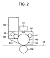
- a fixing unit 20 includes a heat roller 21 and a pressure roller 22.
- the recording medium 2 or 5 passes through a fixing point defined between the heat roller 21 and the pressure roller 22, the toner image on the recording medium 2 or 5 is fixed by heat and pressure into a permanent image.
- the recording medium 2 or 5 is discharged to the outside of the printer 1 or fed into a re-transport path 9.
- the recording medium 2 or 5 is transported by re-transport rollers 28-1, 28-2, and 28-3 disposed along the re-transport path 9, and is then advanced into the transport path 8 again.
- the write sensor 33 and a discharge sensor 34 mechanically senses the recording medium 2 or 5 every time the recording medium 2 or 5 passes the sensors 33 and 34.
- the image processing section 50 interprets commands and the image data, and then renders the image data into bit map data, and finally outputs the bit map data to a printing controller 30.
- the LED head interface 43 converts the image data (bit map data) from the image processing section 50 into data that can drive the LED heads 7K, 7Y, 7M, 7C, and 7W.
- the output image processing section 52 produces print data (image forming data) that contains corrected image data obtained from the correction processing section 51b.
- the output image processing section 52 outputs the print data to the printing controller 30 (S13).
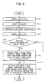
- the correction processing section 51b makes a decision, based on the boundary detection data received from the boundary detecting section 51a, to determine whether the pixel to be corrected is a boundary pixel (S31). If the answer is YES at S31, the program proceeds to S32. If the answer is NO at S31, then the program proceeds to S33.
- the correction processing section 51b makes a decision to determine whether the color shift correction has been performed on all of the pixels contained in the obtained image data. If the answer is NO at S33, the program jumps back to S30. If the answer is YES at S33, the program ends.
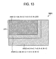
- the area AR5 ( Fig. 14B ) contains white pixels only.
- the pixels in the area AR4 are cyan pixels only.
- the pixels in the area AR4 have the same color, i.e., cyan, as those in the area AR1#2, but have only slightly lower pixels values.
- the area AR2 in Fig. 14A is an area in which the recording medium is directly exposed.
- the area AR5 have white pixels only, and therefore the pixels in the area AR5 form a white streak between the area AR1#2 and AR2, causing poor print quality.
- the area of white pixels is reduced to minimize a white streak.
- color shift correction according to the first embodiment is applied to an image that contains narrow lines, the pixel value of the white image on which the narrow lines are present may all become "0".
- the white pixels having a pixel value of "0" imply that no image of the base color (i.e., white) is printed and therefore the printed image can only be as bright as the color of the recording medium. This causes poor print quality.
- the pixel value be replaced with an average pixel value of white pixels in the vicinity of pixels to be corrected.
- a printer 1 according to a second embodiment has substantially the same general configuration as that according to the first embodiment shown in Fig. 1 .
- the second embodiment differs from the first embodiment in that an image processing section 250 is used.
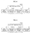
- the image processing section 250 includes a color shift correcting section 251 and an output image processing section 52.
- the image processing section 250 processes the image data received from the image receiving section 42, and then outputs the processed image data to an image outputting section 80.
- the image processing section 250 differs from the image processing section 50 in the operation of the color shift correcting section 251.
- Fig. 17 illustrates the detection area DA in the image IM ( Fig. 9 ) defined at S20 shown in Fig. 7 .
- a pixel in the image IM is taken as a pixel of interest, OP
- a detection area DA is defined with the pixel of interest, OP, at the center of the detection area DA.
- the detection area DA shown in Fig. 17 has 25 pixels: 5 pixels in each column and 5 pixels in each row.
- the cyan, magenta, yellow, black, and white image data are inputted into the color shift correcting section 251.
- image data for four colors except white may be processed as image data, in which case at S41 shown in Fig. 16 may be modified as follows:
- the boundary detecting section 51a checks the pixel value of cyan, magenta, yellow, and black pixels to determine whether the pixels have pixel values larger than the third threshold TH3. If the answer is YES at S41, the program proceeds to S42. If the answer is NO at S41, the program proceeds to S24.
Landscapes
- Engineering & Computer Science (AREA)
- Multimedia (AREA)
- Signal Processing (AREA)
- Textile Engineering (AREA)
- Color Image Communication Systems (AREA)
- Facsimile Image Signal Circuits (AREA)
- Image Processing (AREA)
- Color Electrophotography (AREA)
- Color, Gradation (AREA)
Applications Claiming Priority (1)
| Application Number | Priority Date | Filing Date | Title |
|---|---|---|---|
| JP2012284443A JP5703282B2 (ja) | 2012-12-27 | 2012-12-27 | 画像処理装置、画像形成装置及び画像処理方法 |
Publications (2)
| Publication Number | Publication Date |
|---|---|
| EP2750367A2 true EP2750367A2 (de) | 2014-07-02 |
| EP2750367A3 EP2750367A3 (de) | 2017-02-08 |
Family
ID=49949428
Family Applications (1)
| Application Number | Title | Priority Date | Filing Date |
|---|---|---|---|
| EP13197762.1A Withdrawn EP2750367A3 (de) | 2012-12-27 | 2013-12-17 | Bildverarbeitungsvorrichtung, Bilderzeugungsvorrichtung und Bildverarbeitungsverfahren |
Country Status (4)
| Country | Link |
|---|---|
| US (1) | US8928941B2 (de) |
| EP (1) | EP2750367A3 (de) |
| JP (1) | JP5703282B2 (de) |
| CN (1) | CN103905690B (de) |
Cited By (1)
| Publication number | Priority date | Publication date | Assignee | Title |
|---|---|---|---|---|
| US9406002B2 (en) | 2014-05-22 | 2016-08-02 | Oki Data Corporation | Processing device that corrects pixels of an edge-portion correction area of a print image |
Families Citing this family (3)
| Publication number | Priority date | Publication date | Assignee | Title |
|---|---|---|---|---|
| US9996789B2 (en) * | 2015-09-21 | 2018-06-12 | Cutaneous Information Technologies Llc | Method and apparatus for manufacturing cutaneous information devices |
| CN106485768A (zh) * | 2015-09-02 | 2017-03-08 | 科学工艺博物馆 | 立体图文产生方法 |
| JP6815117B2 (ja) * | 2016-07-21 | 2021-01-20 | 株式会社Screenホールディングス | 印刷データ処理方法、印刷データ処理装置、および印刷データ処理プログラム |
Citations (1)
| Publication number | Priority date | Publication date | Assignee | Title |
|---|---|---|---|---|
| JP2010152209A (ja) | 2008-12-26 | 2010-07-08 | Oki Data Corp | 画像形成装置及び画像形成方法 |
Family Cites Families (8)
| Publication number | Priority date | Publication date | Assignee | Title |
|---|---|---|---|---|
| JPH0817445B2 (ja) * | 1990-11-06 | 1996-02-21 | 大日本スクリーン製造株式会社 | 画像のカブセ処理方法 |
| US6781720B1 (en) * | 1999-11-30 | 2004-08-24 | Xerox Corporation | Gradient-based trapping using patterned trap zones |
| US7787138B2 (en) * | 2005-05-25 | 2010-08-31 | Xerox Corporation | Scheduling system |
| US7762643B2 (en) * | 2004-09-30 | 2010-07-27 | Seiko Epson Corporation | Image forming apparatus, image forming program, image forming method, data generating apparatus, data generating program, data generating method, and recording medium with the program recorded therein |
| JP2006162698A (ja) * | 2004-12-02 | 2006-06-22 | Canon Inc | 画像形成装置及びその制御方法 |
| US7684079B2 (en) * | 2004-12-02 | 2010-03-23 | Canon Kabushiki Kaisha | Image forming apparatus and its control method |
| JP4978516B2 (ja) * | 2008-03-06 | 2012-07-18 | ブラザー工業株式会社 | 印刷データ作成装置、印刷データ作成プログラム、及びコンピュータ読み取り可能な記録媒体 |
| US9401012B2 (en) * | 2012-10-18 | 2016-07-26 | Athentech Technologies Inc. | Method for correcting purple distortion in digital images and a computing device employing same |
-
2012
- 2012-12-27 JP JP2012284443A patent/JP5703282B2/ja active Active
-
2013
- 2013-12-17 EP EP13197762.1A patent/EP2750367A3/de not_active Withdrawn
- 2013-12-20 US US14/135,684 patent/US8928941B2/en active Active
- 2013-12-27 CN CN201310734280.4A patent/CN103905690B/zh active Active
Patent Citations (1)
| Publication number | Priority date | Publication date | Assignee | Title |
|---|---|---|---|---|
| JP2010152209A (ja) | 2008-12-26 | 2010-07-08 | Oki Data Corp | 画像形成装置及び画像形成方法 |
Cited By (1)
| Publication number | Priority date | Publication date | Assignee | Title |
|---|---|---|---|---|
| US9406002B2 (en) | 2014-05-22 | 2016-08-02 | Oki Data Corporation | Processing device that corrects pixels of an edge-portion correction area of a print image |
Also Published As
| Publication number | Publication date |
|---|---|
| CN103905690B (zh) | 2018-09-28 |
| CN103905690A (zh) | 2014-07-02 |
| JP5703282B2 (ja) | 2015-04-15 |
| JP2014127918A (ja) | 2014-07-07 |
| US20140185067A1 (en) | 2014-07-03 |
| EP2750367A3 (de) | 2017-02-08 |
| US8928941B2 (en) | 2015-01-06 |
Similar Documents
| Publication | Publication Date | Title |
|---|---|---|
| US20050088710A1 (en) | Color image forming apparatus and method of controlling same | |
| JP5803268B2 (ja) | 画像形成装置、画像形成方法、およびプログラム | |
| KR20150010188A (ko) | 화상형성장치 및 컬러 레지스트레이션 보정 방법 | |
| CN107664934B (zh) | 图像形成装置 | |
| KR20120013827A (ko) | 색 정합 오차 보상을 수행하는 컨트롤러 칩 및 화상형성장치와 그 방법들 | |
| JP4377908B2 (ja) | 画像形成装置および画像形成条件の補正方法 | |
| EP2750367A2 (de) | Bildverarbeitungsvorrichtung, Bilderzeugungsvorrichtung und Bildverarbeitungsverfahren | |
| EP2299686A2 (de) | Bilderzeugungsvorrichtung | |
| JP5171165B2 (ja) | 画像形成装置 | |
| JP5325044B2 (ja) | 画像形成装置 | |
| JP2010102182A (ja) | 画像形成装置 | |
| JP2005131961A (ja) | 画像形成装置 | |
| JPH11295956A (ja) | カラー画像形成装置 | |
| JP5060174B2 (ja) | 画像形成装置 | |
| JP2013020153A (ja) | 画像形成装置 | |
| JP5210031B2 (ja) | 画像形成装置 | |
| JP6418875B2 (ja) | 画像形成装置 | |
| US20170199480A1 (en) | Image forming apparatus and image forming method | |
| JP4872492B2 (ja) | 画像形成装置 | |
| JP2007006204A (ja) | 画像形成装置 | |
| US11003114B2 (en) | Image processing apparatus that controls fixing temperature based on the similarity of image data of the current page and the next page, image processing method, and recording medium | |
| EP2541332B1 (de) | Bilderzeugungsvorrichtung | |
| JP2010019968A (ja) | 画像形成装置、画像補正方法、画像補正プログラム及び記録媒体 | |
| JP2024175516A (ja) | 画像形成装置 | |
| JP4957189B2 (ja) | 画像形成装置、画像形成装置の制御方法、および画像形成装置の制御プログラム |
Legal Events
| Date | Code | Title | Description |
|---|---|---|---|
| 17P | Request for examination filed |
Effective date: 20131217 |
|
| AK | Designated contracting states |
Kind code of ref document: A2 Designated state(s): AL AT BE BG CH CY CZ DE DK EE ES FI FR GB GR HR HU IE IS IT LI LT LU LV MC MK MT NL NO PL PT RO RS SE SI SK SM TR |
|
| AX | Request for extension of the european patent |
Extension state: BA ME |
|
| PUAI | Public reference made under article 153(3) epc to a published international application that has entered the european phase |
Free format text: ORIGINAL CODE: 0009012 |
|
| PUAL | Search report despatched |
Free format text: ORIGINAL CODE: 0009013 |
|
| RIC1 | Information provided on ipc code assigned before grant |
Ipc: H04N 1/58 20060101ALI20161223BHEP Ipc: H04N 1/54 20060101AFI20161223BHEP |
|
| AK | Designated contracting states |
Kind code of ref document: A3 Designated state(s): AL AT BE BG CH CY CZ DE DK EE ES FI FR GB GR HR HU IE IS IT LI LT LU LV MC MK MT NL NO PL PT RO RS SE SI SK SM TR |
|
| AX | Request for extension of the european patent |
Extension state: BA ME |
|
| STAA | Information on the status of an ep patent application or granted ep patent |
Free format text: STATUS: REQUEST FOR EXAMINATION WAS MADE |
|
| R17P | Request for examination filed (corrected) |
Effective date: 20170727 |
|
| RBV | Designated contracting states (corrected) |
Designated state(s): AL AT BE BG CH CY CZ DE DK EE ES FI FR GB GR HR HU IE IS IT LI LT LU LV MC MK MT NL NO PL PT RO RS SE SI SK SM TR |
|
| STAA | Information on the status of an ep patent application or granted ep patent |
Free format text: STATUS: EXAMINATION IS IN PROGRESS |
|
| 17Q | First examination report despatched |
Effective date: 20180309 |
|
| GRAP | Despatch of communication of intention to grant a patent |
Free format text: ORIGINAL CODE: EPIDOSNIGR1 |
|
| STAA | Information on the status of an ep patent application or granted ep patent |
Free format text: STATUS: GRANT OF PATENT IS INTENDED |
|
| INTG | Intention to grant announced |
Effective date: 20190701 |
|
| STAA | Information on the status of an ep patent application or granted ep patent |
Free format text: STATUS: THE APPLICATION IS DEEMED TO BE WITHDRAWN |
|
| 18D | Application deemed to be withdrawn |
Effective date: 20191112 |