EP2737539B1 - Hochspannungs-mosfet und verfahren zu dessen herstellung - Google Patents
Hochspannungs-mosfet und verfahren zu dessen herstellung Download PDFInfo
- Publication number
- EP2737539B1 EP2737539B1 EP12750895.0A EP12750895A EP2737539B1 EP 2737539 B1 EP2737539 B1 EP 2737539B1 EP 12750895 A EP12750895 A EP 12750895A EP 2737539 B1 EP2737539 B1 EP 2737539B1
- Authority
- EP
- European Patent Office
- Prior art keywords
- well
- doped
- substrate
- heavily doped
- region
- Prior art date
- Legal status (The legal status is an assumption and is not a legal conclusion. Google has not performed a legal analysis and makes no representation as to the accuracy of the status listed.)
- Active
Links
Images




Classifications
-
- H—ELECTRICITY
- H10—SEMICONDUCTOR DEVICES; ELECTRIC SOLID-STATE DEVICES NOT OTHERWISE PROVIDED FOR
- H10D—INORGANIC ELECTRIC SEMICONDUCTOR DEVICES
- H10D30/00—Field-effect transistors [FET]
- H10D30/60—Insulated-gate field-effect transistors [IGFET]
- H10D30/601—Insulated-gate field-effect transistors [IGFET] having lightly-doped drain or source extensions, e.g. LDD IGFETs or DDD IGFETs
-
- H—ELECTRICITY
- H10—SEMICONDUCTOR DEVICES; ELECTRIC SOLID-STATE DEVICES NOT OTHERWISE PROVIDED FOR
- H10D—INORGANIC ELECTRIC SEMICONDUCTOR DEVICES
- H10D30/00—Field-effect transistors [FET]
- H10D30/01—Manufacture or treatment
- H10D30/021—Manufacture or treatment of FETs having insulated gates [IGFET]
- H10D30/0221—Manufacture or treatment of FETs having insulated gates [IGFET] having asymmetry in the channel direction, e.g. lateral high-voltage MISFETs having drain offset region or extended-drain MOSFETs [EDMOS]
-
- H—ELECTRICITY
- H10—SEMICONDUCTOR DEVICES; ELECTRIC SOLID-STATE DEVICES NOT OTHERWISE PROVIDED FOR
- H10D—INORGANIC ELECTRIC SEMICONDUCTOR DEVICES
- H10D30/00—Field-effect transistors [FET]
- H10D30/01—Manufacture or treatment
- H10D30/021—Manufacture or treatment of FETs having insulated gates [IGFET]
- H10D30/028—Manufacture or treatment of FETs having insulated gates [IGFET] of double-diffused metal oxide semiconductor [DMOS] FETs
- H10D30/0281—Manufacture or treatment of FETs having insulated gates [IGFET] of double-diffused metal oxide semiconductor [DMOS] FETs of lateral DMOS [LDMOS] FETs
-
- H—ELECTRICITY
- H10—SEMICONDUCTOR DEVICES; ELECTRIC SOLID-STATE DEVICES NOT OTHERWISE PROVIDED FOR
- H10D—INORGANIC ELECTRIC SEMICONDUCTOR DEVICES
- H10D30/00—Field-effect transistors [FET]
- H10D30/60—Insulated-gate field-effect transistors [IGFET]
- H10D30/601—Insulated-gate field-effect transistors [IGFET] having lightly-doped drain or source extensions, e.g. LDD IGFETs or DDD IGFETs
- H10D30/603—Insulated-gate field-effect transistors [IGFET] having lightly-doped drain or source extensions, e.g. LDD IGFETs or DDD IGFETs having asymmetry in the channel direction, e.g. lateral high-voltage MISFETs having drain offset region or extended drain IGFETs [EDMOS]
-
- H—ELECTRICITY
- H10—SEMICONDUCTOR DEVICES; ELECTRIC SOLID-STATE DEVICES NOT OTHERWISE PROVIDED FOR
- H10D—INORGANIC ELECTRIC SEMICONDUCTOR DEVICES
- H10D30/00—Field-effect transistors [FET]
- H10D30/60—Insulated-gate field-effect transistors [IGFET]
- H10D30/64—Double-diffused metal-oxide semiconductor [DMOS] FETs
- H10D30/65—Lateral DMOS [LDMOS] FETs
-
- H—ELECTRICITY
- H10—SEMICONDUCTOR DEVICES; ELECTRIC SOLID-STATE DEVICES NOT OTHERWISE PROVIDED FOR
- H10D—INORGANIC ELECTRIC SEMICONDUCTOR DEVICES
- H10D30/00—Field-effect transistors [FET]
- H10D30/60—Insulated-gate field-effect transistors [IGFET]
- H10D30/721—Insulated-gate field-effect transistors [IGFET] having a gate-to-body connection, i.e. bulk dynamic threshold voltage IGFET
-
- H—ELECTRICITY
- H10—SEMICONDUCTOR DEVICES; ELECTRIC SOLID-STATE DEVICES NOT OTHERWISE PROVIDED FOR
- H10D—INORGANIC ELECTRIC SEMICONDUCTOR DEVICES
- H10D62/00—Semiconductor bodies, or regions thereof, of devices having potential barriers
- H10D62/10—Shapes, relative sizes or dispositions of the regions of the semiconductor bodies; Shapes of the semiconductor bodies
- H10D62/13—Semiconductor regions connected to electrodes carrying current to be rectified, amplified or switched, e.g. source or drain regions
- H10D62/149—Source or drain regions of field-effect devices
- H10D62/151—Source or drain regions of field-effect devices of IGFETs
-
- H—ELECTRICITY
- H10—SEMICONDUCTOR DEVICES; ELECTRIC SOLID-STATE DEVICES NOT OTHERWISE PROVIDED FOR
- H10D—INORGANIC ELECTRIC SEMICONDUCTOR DEVICES
- H10D62/00—Semiconductor bodies, or regions thereof, of devices having potential barriers
- H10D62/10—Shapes, relative sizes or dispositions of the regions of the semiconductor bodies; Shapes of the semiconductor bodies
- H10D62/13—Semiconductor regions connected to electrodes carrying current to be rectified, amplified or switched, e.g. source or drain regions
- H10D62/149—Source or drain regions of field-effect devices
- H10D62/151—Source or drain regions of field-effect devices of IGFETs
- H10D62/156—Drain regions of DMOS transistors
- H10D62/157—Impurity concentrations or distributions
-
- H—ELECTRICITY
- H10—SEMICONDUCTOR DEVICES; ELECTRIC SOLID-STATE DEVICES NOT OTHERWISE PROVIDED FOR
- H10W—GENERIC PACKAGES, INTERCONNECTIONS, CONNECTORS OR OTHER CONSTRUCTIONAL DETAILS OF DEVICES COVERED BY CLASS H10
- H10W46/00—Marks applied to devices, e.g. for alignment or identification
-
- H—ELECTRICITY
- H10—SEMICONDUCTOR DEVICES; ELECTRIC SOLID-STATE DEVICES NOT OTHERWISE PROVIDED FOR
- H10D—INORGANIC ELECTRIC SEMICONDUCTOR DEVICES
- H10D64/00—Electrodes of devices having potential barriers
- H10D64/20—Electrodes characterised by their shapes, relative sizes or dispositions
- H10D64/27—Electrodes not carrying the current to be rectified, amplified, oscillated or switched, e.g. gates
- H10D64/311—Gate electrodes for field-effect devices
- H10D64/411—Gate electrodes for field-effect devices for FETs
- H10D64/511—Gate electrodes for field-effect devices for FETs for IGFETs
- H10D64/514—Gate electrodes for field-effect devices for FETs for IGFETs characterised by the insulating layers
- H10D64/516—Gate electrodes for field-effect devices for FETs for IGFETs characterised by the insulating layers the thicknesses being non-uniform
-
- H—ELECTRICITY
- H10—SEMICONDUCTOR DEVICES; ELECTRIC SOLID-STATE DEVICES NOT OTHERWISE PROVIDED FOR
- H10W—GENERIC PACKAGES, INTERCONNECTIONS, CONNECTORS OR OTHER CONSTRUCTIONAL DETAILS OF DEVICES COVERED BY CLASS H10
- H10W46/00—Marks applied to devices, e.g. for alignment or identification
- H10W46/301—Marks applied to devices, e.g. for alignment or identification for alignment
-
- H—ELECTRICITY
- H10—SEMICONDUCTOR DEVICES; ELECTRIC SOLID-STATE DEVICES NOT OTHERWISE PROVIDED FOR
- H10W—GENERIC PACKAGES, INTERCONNECTIONS, CONNECTORS OR OTHER CONSTRUCTIONAL DETAILS OF DEVICES COVERED BY CLASS H10
- H10W46/00—Marks applied to devices, e.g. for alignment or identification
- H10W46/501—Marks applied to devices, e.g. for alignment or identification for use before dicing
Definitions
- the present disclosure relates to fabrication of high voltage (HV) metal oxide semiconductor (MOS) devices, and more particularly, to fabrication of multiple well drains in the HV MOS devices.
- HV high voltage
- MOS metal oxide semiconductor
- High voltage (HV) metal oxide semiconductor (MOS) devices typically use well implants to create the drain and drift structures. Hot carrier impact ionization limits the voltage range of these devices, and typical lightly doped drain (Ldd) implants are not useful in drain engineering as the drain is under the field oxide.
- Ldd lightly doped drain
- Typical prior technology self aligned well structures create undesirable steps (change in elevation) at the well edges in the silicon (Si) substrate surface and cause alignment issues for successive well implants.
- FIG. 1 depicted are schematic elevational diagrams of prior art process steps used to form an n-well implant in a p-substrate.
- Figure 1(a) represents a schematic elevational diagram of the n-well implant 104 in a P-substrate 102 that is masked by a nitride layer 106.
- Figure 1(b) represents an oxide layer 108 grown over the n-well implant 104 then the nitride layer 106 is stripped therefrom.
- Figure 1(c) represents the N-well implant 104a in the P-substrate 102 after the oxide layer 108 is etched off.
- the oxide growth consumes an amount of the oxide layer 108 causing some of the top portion of the N-well implant 104 to be removed, thereby resulting in steps formed at the N-well edges 110. These n-well edges 110 (steps) are used for subsequent mask alignment purposes.
- US Patent US 5,811,850 discloses an improved LDMOS transistor and associated process for fabrication.
- JP2004200359 discloses a semiconductor device and method for manufacturing the same.
- US 2006/0068552 A1 discloses a semiconductor device manufacturing method in which a polysilicon film and a silicon nitride film are deposited on an upper surface of an epitaxial layer. Patterning is performed so that the polysilicon film and the silicon nitride film are left in regions in which a LOCOS oxide film is to be formed. Then, using steps of the polysilicon film and the silicon nitride film as alignment marks, a diffusion layer as drain regions is formed. Subsequently, the LOCOS oxide film is formed. This manufacturing method enables the diffusion layer to be formed with high position accuracy without being affected by a shape of the LOCOS oxide film.
- a method for fabricating a high voltage (HV) metal oxide semiconductor (MOS) field effect transistor (FET) device comprises the steps of:
- a high voltage (HV) metal oxide semiconductor (MOS) field effect transistor (FET) device comprising:
- the alignment target may be used for aligning implantation of the lightly doped N-well, the doped N-well, the heavily doped N+ region, the another heavily doped N+ region, the field oxides, the gate oxide, and the polysilicon gate.
- a drain connection may be made to the heavily doped N+ region
- a gate connection may be made to the polysilicon gate
- a source connection may be made to the another heavily doped N+ region.
- a plurality of high voltage metal oxide semiconductor field effect transistor devices may be formed.
- the lightly doped N-well and doped N-well may form a graded junction in a drift area of the MOSFET device.
- lengths of the lightly doped and doped N-wells may be adjusted to reduce high field effects of the MOSFET device. According to a further embodiment, lengths of the lightly doped N-well and the doped N-well may be adjusted to reduce on resistance of the MOSFET device.
- a graded N-well junction can be created under the field oxide.
- Multiple N-well implants are formed in a P-substrate or a single N-well implant is formed in a lightly doped N-substrate by first etching the silicon substrate with an alignment target for aligning future process masks thereto. The alignment target is outside of any active device area.
- N-well implants of different doping levels a graded junction in the drift area of a metal oxide semiconductor (MOS) field effect transistor (FET) can be created and a pseudo Ldd structure may thereby be realized.
- MOS metal oxide semiconductor
- FET field effect transistor
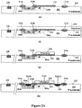
- FIGS 2 and 2A depicted are schematic elevational diagrams of process fabrication steps used in forming multiple N-well implants in a P-substrate, according to a specific example embodiment of this disclosure.
- a "zero" layer 222 is created by etching the silicon P-substrate 202 with an alignment target 220 for aligning future masks thereto.
- the alignment target 220 is outside of any active device area.
- multiple implants may be performed as more fully described hereinafter.
- a graded junction in the drift area of a metal oxide semiconductor (MOS) field effect transistor (FET) can be created and a pseudo Ldd structure may thereby be realized.
- MOS metal oxide semiconductor
- FET field effect transistor
- a lightly doped N - -well 204a is formed through means, e.g., implant and drive (heat), that are well known to one having ordinary skill in integrated circuit semiconductor fabrication.
- a second more heavily doped N-well 204b is formed through well known means, e.g., implant and drive (heat).
- field oxides 214a, 214b and 214c are grown (formed) through well known means.
- a gate oxide 216 is grown (formed) through well known means.
- polysilicon 218 is grown (formed) over the gate oxide 216 through well known means.
- the polysilicon 218 is formed into a polysilicon gate 218 by, for example but not limited to, photolithography and etching over the gate oxide 216 through well known means.
- implant and drive heat
- the wells can be implanted after the field oxide/isolation is in place, and the wells can be implanted and dopants activated without a drive (heat).
- the aforementioned fabrication steps create a high voltage (HV) MOS FET shown in Figure 2(h) .
- the alignment target 220 is used to align the respective masks thereof.
- the multiple N-well implants 204 create a graded junction in a drift area of the HV MOS FET. By fine tuning the lengths of the heavy and light N-well implants, high field effects can be significantly reduced as well as a reduction in the on resistance of the HV MOS FET device.
- FIG. 3 depicted is a voltage-current graph of Vds and Ids showing an improvement of the drive current in the HV MOS FET device with the multiple N-well drain engineering, according to the teachings of this disclosure.
- Advantages of the present invention are: 1) More accurate alignment of well implants, 2) ability to use multiple well implants to generate an engineered drift/drain, 3) better drive current, 4) elimination of hot carrier affects, and 5) a wider voltage range of device operation.
- FIGS. 4 and 4A depicted are schematic elevational diagrams of process fabrication steps used in forming N-well implants and a lightly doped P-well implant in an N - -substrate, according to another specific example not forming part of the present invention but useful for understanding it.
- a "zero" layer 422 is created by etching a lightly doped N - -substrate 402 with an alignment target 420 for aligning future masks thereto.
- the alignment target 420 is outside of any active device area. Thereafter multiple implants may be performed as more fully described hereinafter.
- the lightly doped N - -substrate 402 By using a N-well 404a of a different doping level then the lightly doped N - -substrate 402, a graded junction in the drift area of a metal oxide semiconductor (MOS) field effect transistor (FET) can be created and a pseudo Ldd structure may thereby be realized.
- MOS metal oxide semiconductor
- FET field effect transistor
- a more heavily doped N-well 404a is formed in the lightly doped N - -substrate 402 through well known means, e.g., implant and drive (heat).
- field oxides 414a, 414b and 414c are grown (formed) through well known means.
- a gate oxide 416 is grown (formed) through well known means.
- polysilicon 418 is grown (formed) over the gate oxide 416 through well known means.
- the polysilicon 418 is formed into a polysilicon gate 418 by, for example but not limited to, photolithography and etching over the gate oxide 416 through well known means.
- a low concentration implant P-type region 424 is formed in the lightly doped N - -substrate 402 through well known means e.g., photo, implant and drive (heat).
- the P-type region 424 may also be formed without requiring a drive (heat) for certain implant conditions.
- Shown in Figure 4(h) heavily doped N + regions 404b and 412 are formed in the N-well 404a and the P-type well 424, respectively, through well known implant means, for drain and source connections, respectively.
- a heavily doped P + region 426 is formed in the P-type region 424 through well known implant means.
- the heavily doped P + region 426 is used as a connection to the P-type region 424.
- the heavily doped P + region 426 may be butted adjacent the heavily doped N + region 412 and also connected to the source contact (as shown in Figure 4A ), or separated from the heavily doped N + region 412 and connected to a voltage source (not shown) to change the potential of the P-type region 424.
- the alignment target 420 is used to align the respective masks thereof.
- the N-well implant 404a and the lightly doped N - -substrate 402 create a graded junction in a drift area of the HV MOS FET. By fine tuning the length of the N-well implant 404a, high field effects can be significantly reduced as well as a reduction in the on resistance of the HV MOS FET device.
Landscapes
- Insulated Gate Type Field-Effect Transistor (AREA)
- Metal-Oxide And Bipolar Metal-Oxide Semiconductor Integrated Circuits (AREA)
Claims (9)
- Verfahren zur Herstellung einer Hochspannungs- (HV-) Metalloxidhalbleiter- (MOS-) Feldeffekttransistor- (FET-) Vorrichtung, wobei das Verfahren die folgenden Schritte aufweist:Ausbilden einer Nullschicht (222) auf einem P-Substrat (202) durch Ätzen eines Ausrichtungsziels (220) auf einer Oberfläche des P-Substrats (202) und außerhalb aktiver Vorrichtungsbereiche des P-Substrats (202);Ausbilden einer leicht dotierten N-Wanne (204a) in einem Teil des P-Substrats (202) durch Implantation;Ausbilden einer dotierten N-Wanne (204b) in einem Teil der leicht dotierten N-Wanne (204a) durch Implantation, wobei die dotierte N-Wanne (204b) stärker dotiert ist als die leicht dotierte N-Wanne (204a);Ausbilden von Feldoxiden (214a, 214b, 214c) über bestimmten Teilen des P-Substrats (202),wobei zumindest ein Feldoxid (214b) die leicht und stärker dotierten N-Wannen (204a, 204b) an einem Übergang zwischen der N-Wanne (204b) und der leicht dotierten N-Wanne (204a) überlappt;Ausbilden eines Gate-Oxids (216) über einem Teil der leicht dotierten N-Wanne (204a) und einem Teil des P-Substrats (202);Ausbilden eines Polysilicium-Gates (218) über dem Gate-Oxid (216); undAusbilden eines stark dotierten N+-Bereichs (204c) in einem Teil der dotierten N-Wanne (204b) und eines anderen stark dotierten N+-Bereichs (212) in einem anderen Teil des P-Substrats (202) durch Implantation,wobei die Schritte des Ausbildens das Verwenden von Masken aufweisen, die auf das Ausrichtungsziel (220) ausgerichtet sind.
- Verfahren gemäß Anspruch 1, wobei eine Drain-Verbindung zu dem stark dotierten N+-Bereich (204c) hergestellt wird, eine Gate-Verbindung zu dem Polysilicium-Gate (218) hergestellt wird und eine Source-Verbindung zu dem anderen stark dotierten N+-Bereich (212) hergestellt wird.
- Verfahren gemäß Anspruch 1, wobei die leicht dotierte N-Wanne (204a) und die stärker dotierte N-Wanne (204b) eine ähnliche Tiefe innerhalb des P-Substrats (202) aufweisen und unter Verwendung mehrerer Wannenimplantationen mit unterschiedlichen Dotierungsniveaus in einem Driftbereich der MOSFET-Vorrichtung einen abgestuften Übergang ausbilden.
- Verfahren gemäß Anspruch 1, das weiterhin die Schritte des Bestimmens der Längen der leicht dotierten und stärker dotierten N-Wannen (204a und 204b) in Bezug aufeinander aufweist, um einen abgestuften Übergang zu erzeugen, wodurch hohe Feldeffekte und/oder Einschaltwiderstände der MOSFET-Vorrichtung verringert werden.
- Hochspannungs- (HV-) Metalloxidhalbleiter- (MOS-) Feldeffekttransistor- (FET-) Vorrichtung, die aufweist:eine Nullschicht (222) auf einem P-Substrat (202), die ein geätztes Ausrichtungsziel auf einer Oberfläche davon und außerhalb der aktiven Vorrichtungsbereiche des P-Substrats (202) aufweist;eine leicht dotierte N-Wanne (204a), die in einen Teil des P-Substrats implantiert ist;eine dotierte N-Wanne (204b), die in einen Teil der leicht dotierten N-Wanne (204a) implantiert ist, wobei die dotierte N-Wanne (204b) stärker dotiert ist als die leicht dotierte N-Wanne (204a);einen stark dotierten N+-Bereich (204c), der in einen Teil der dotierten N-Wanne (204b) implantiert ist;einen anderen stark dotierten N+-Bereich (212), der in einen anderen Teil des P-Substrats (202) implantiert ist;Feldoxide (214a, 214b, 214c), die neben dem stark dotierten N+-Bereich (204c) und dem anderen stark dotierten N+-Bereich (212) ausgebildet sind, wobei zumindest ein Feldoxid (214b) die leicht und stärker dotierten N-Wannen ((204a, 204b) an einem Übergang zwischen der N-Wanne (204b) und der leicht dotierten N-Wanne (204a) überlappt;ein Gate-Oxid (216), das über einem Teil der leicht dotierten N-Wanne (204a) und einem Teil des P-Substrats (202) ausgebildet ist; undein Polysilicium-Gate (218), das über dem Gate-Oxid (216) ausgebildet ist,wobei das Ausrichtungsziel (220) zum Ausrichten der Implantation der leicht dotierten N-Wanne (204a), der dotierten N-Wanne (204b), des stark dotierten N+-Bereichs (204c) und des anderen stark dotierten N+-Bereichs (212), der Feldoxide (214a, 214b, 214c), des Gate-Oxids (216) und des Polysilicium-Gates (218) ausgebildet ist.
- HV-MOSFET-Vorrichtung gemäß Anspruch 5, die weiterhin eine Drain-Verbindung mit dem stark dotierten N+-Bereich (204c), eine Gate-Verbindung mit dem Polysilicium-Gate (218) und eine Source-Verbindung mit dem anderen stark dotierten N+-Bereich (212) aufweist.
- HV-MOSFET-Vorrichtung gemäß einem der vorhergehenden Ansprüche 5 bis 6, die eine Vielzahl von Hochspannungs-Metalloxid-Halbleiter-Feldeffekttransistorvorrichtungen aufweist.
- HV-MOSFET-Vorrichtung gemäß Anspruch 5, wobei die leicht dotierte N-Wanne (204a) und die stärker dotierte N-Wanne (204b) eine ähnliche Tiefe innerhalb des P-Substrats (202) aufweisen und einen abgestuften Übergang aus unterschiedlichen Dotierungsniveaus in einem Driftbereich der MOSFET-Vorrichtung ausbilden.
- HV-MOSFET-Vorrichtung gemäß einem der vorhergehenden Ansprüche 5 bis 8, wobei die Längen der leicht dotierten (204a) und stärker dotierten N-Wannen (204b) in Bezug aufeinander derart vorgegeben sind, dass hohe Feldeffekte und/oder Einschaltwiderstand der MOSFET-Vorrichtung reduziert werden/wird.
Applications Claiming Priority (3)
| Application Number | Priority Date | Filing Date | Title |
|---|---|---|---|
| US201161511195P | 2011-07-25 | 2011-07-25 | |
| US13/554,890 US8962397B2 (en) | 2011-07-25 | 2012-07-20 | Multiple well drain engineering for HV MOS devices |
| PCT/US2012/047826 WO2013016273A2 (en) | 2011-07-25 | 2012-07-23 | Multiple well drain engineering for hv mos devices |
Publications (2)
| Publication Number | Publication Date |
|---|---|
| EP2737539A2 EP2737539A2 (de) | 2014-06-04 |
| EP2737539B1 true EP2737539B1 (de) | 2021-01-13 |
Family
ID=47596528
Family Applications (1)
| Application Number | Title | Priority Date | Filing Date |
|---|---|---|---|
| EP12750895.0A Active EP2737539B1 (de) | 2011-07-25 | 2012-07-23 | Hochspannungs-mosfet und verfahren zu dessen herstellung |
Country Status (6)
| Country | Link |
|---|---|
| US (1) | US8962397B2 (de) |
| EP (1) | EP2737539B1 (de) |
| KR (1) | KR101987811B1 (de) |
| CN (1) | CN103814444B (de) |
| TW (1) | TWI615973B (de) |
| WO (1) | WO2013016273A2 (de) |
Families Citing this family (6)
| Publication number | Priority date | Publication date | Assignee | Title |
|---|---|---|---|---|
| US11181688B2 (en) * | 2009-10-13 | 2021-11-23 | Skorpios Technologies, Inc. | Integration of an unprocessed, direct-bandgap chip into a silicon photonic device |
| JP2015141996A (ja) * | 2014-01-28 | 2015-08-03 | 株式会社東芝 | 半導体装置及びその製造方法 |
| CN105244261B (zh) * | 2014-06-18 | 2019-06-28 | 上海华力微电子有限公司 | 半导体器件的制备方法 |
| US11120478B2 (en) * | 2015-01-12 | 2021-09-14 | Ebay Inc. | Joint-based item recognition |
| CN105825098B (zh) * | 2016-03-16 | 2018-03-27 | 广东欧珀移动通信有限公司 | 一种电子终端的屏幕解锁方法、图像采集方法及装置 |
| CN109192663B (zh) * | 2018-09-12 | 2021-07-16 | 长江存储科技有限责任公司 | 制作高压器件与半导体器件的方法 |
Citations (1)
| Publication number | Priority date | Publication date | Assignee | Title |
|---|---|---|---|---|
| US20060068552A1 (en) * | 2004-09-29 | 2006-03-30 | Takashi Ogura | Method of manufacturing semiconductor device |
Family Cites Families (8)
| Publication number | Priority date | Publication date | Assignee | Title |
|---|---|---|---|---|
| US5585294A (en) | 1994-10-14 | 1996-12-17 | Texas Instruments Incorporated | Method of fabricating lateral double diffused MOS (LDMOS) transistors |
| KR100225411B1 (ko) * | 1997-03-24 | 1999-10-15 | 김덕중 | LDMOS(a lateral double-diffused MOS) 트랜지스터 소자 및 그의 제조 방법 |
| US6020611A (en) | 1998-06-10 | 2000-02-01 | Motorola, Inc. | Semiconductor component and method of manufacture |
| JP2004200359A (ja) | 2002-12-18 | 2004-07-15 | Ricoh Co Ltd | 半導体装置及びその製造方法 |
| JP5063865B2 (ja) * | 2005-03-30 | 2012-10-31 | オンセミコンダクター・トレーディング・リミテッド | 半導体装置 |
| KR101009399B1 (ko) * | 2008-10-01 | 2011-01-19 | 주식회사 동부하이텍 | Ldmos 트랜지스터 및 그 제조방법 |
| US8643101B2 (en) * | 2011-04-20 | 2014-02-04 | United Microelectronics Corp. | High voltage metal oxide semiconductor device having a multi-segment isolation structure |
| US8592905B2 (en) * | 2011-06-26 | 2013-11-26 | United Microelectronics Corp. | High-voltage semiconductor device |
-
2012
- 2012-07-20 US US13/554,890 patent/US8962397B2/en active Active
- 2012-07-23 EP EP12750895.0A patent/EP2737539B1/de active Active
- 2012-07-23 WO PCT/US2012/047826 patent/WO2013016273A2/en not_active Ceased
- 2012-07-23 CN CN201280044545.1A patent/CN103814444B/zh active Active
- 2012-07-23 KR KR1020147004757A patent/KR101987811B1/ko active Active
- 2012-07-25 TW TW101126863A patent/TWI615973B/zh active
Patent Citations (1)
| Publication number | Priority date | Publication date | Assignee | Title |
|---|---|---|---|---|
| US20060068552A1 (en) * | 2004-09-29 | 2006-03-30 | Takashi Ogura | Method of manufacturing semiconductor device |
Also Published As
| Publication number | Publication date |
|---|---|
| CN103814444B (zh) | 2017-06-13 |
| EP2737539A2 (de) | 2014-06-04 |
| TWI615973B (zh) | 2018-02-21 |
| US8962397B2 (en) | 2015-02-24 |
| WO2013016273A2 (en) | 2013-01-31 |
| WO2013016273A3 (en) | 2013-05-30 |
| CN103814444A (zh) | 2014-05-21 |
| KR101987811B1 (ko) | 2019-06-11 |
| US20130026545A1 (en) | 2013-01-31 |
| TW201310650A (zh) | 2013-03-01 |
| KR20140051353A (ko) | 2014-04-30 |
Similar Documents
| Publication | Publication Date | Title |
|---|---|---|
| US9466700B2 (en) | Semiconductor device and method of fabricating same | |
| US9484454B2 (en) | Double-resurf LDMOS with drift and PSURF implants self-aligned to a stacked gate “bump” structure | |
| US8173500B2 (en) | Poly-emitter type bipolar junction transistor, bipolar CMOS DMOS device, and manufacturing methods of poly-emitter type bipolar junction transistor and bipolar CMOS DMOS device | |
| US7414287B2 (en) | System and method for making a LDMOS device with electrostatic discharge protection | |
| US7384836B2 (en) | Integrated circuit transistor insulating region fabrication method | |
| EP2737539B1 (de) | Hochspannungs-mosfet und verfahren zu dessen herstellung | |
| CN102891180B (zh) | 一种包含mosfet器件的半导体器件和制作方法 | |
| CN103579005B (zh) | 采用高电压反注入的功率晶体管 | |
| US20070296046A1 (en) | Semiconductor device and method of manufacture thereof | |
| US10910493B2 (en) | Semiconductor device and method of manufacturing the same | |
| US20020117714A1 (en) | High voltage MOS transistor | |
| US10522663B2 (en) | Integrated JFET structure with implanted backgate | |
| KR101015529B1 (ko) | Ldmos 트랜지스터 및 그 제조방법 | |
| US20130093014A1 (en) | Semiconductor device and method for fabricating the same | |
| CN102881588A (zh) | 一种双极结型晶体管的制作方法 | |
| KR100266689B1 (ko) | 고전압 수평 확산 모스 트랜지스터 제조방법 | |
| CN104392961A (zh) | 一种cmos集成电路的制造方法 | |
| JP2004296914A (ja) | 半導体装置およびその製造方法 | |
| KR101010439B1 (ko) | 반도체 소자의 제조 방법 | |
| KR20110078449A (ko) | Ldmos 트랜지스터의 제조방법 |
Legal Events
| Date | Code | Title | Description |
|---|---|---|---|
| PUAI | Public reference made under article 153(3) epc to a published international application that has entered the european phase |
Free format text: ORIGINAL CODE: 0009012 |
|
| 17P | Request for examination filed |
Effective date: 20140219 |
|
| AK | Designated contracting states |
Kind code of ref document: A2 Designated state(s): AL AT BE BG CH CY CZ DE DK EE ES FI FR GB GR HR HU IE IS IT LI LT LU LV MC MK MT NL NO PL PT RO RS SE SI SK SM TR |
|
| DAX | Request for extension of the european patent (deleted) | ||
| STAA | Information on the status of an ep patent application or granted ep patent |
Free format text: STATUS: EXAMINATION IS IN PROGRESS |
|
| 17Q | First examination report despatched |
Effective date: 20180522 |
|
| GRAP | Despatch of communication of intention to grant a patent |
Free format text: ORIGINAL CODE: EPIDOSNIGR1 |
|
| STAA | Information on the status of an ep patent application or granted ep patent |
Free format text: STATUS: GRANT OF PATENT IS INTENDED |
|
| INTG | Intention to grant announced |
Effective date: 20200806 |
|
| GRAS | Grant fee paid |
Free format text: ORIGINAL CODE: EPIDOSNIGR3 |
|
| GRAA | (expected) grant |
Free format text: ORIGINAL CODE: 0009210 |
|
| STAA | Information on the status of an ep patent application or granted ep patent |
Free format text: STATUS: THE PATENT HAS BEEN GRANTED |
|
| AK | Designated contracting states |
Kind code of ref document: B1 Designated state(s): AL AT BE BG CH CY CZ DE DK EE ES FI FR GB GR HR HU IE IS IT LI LT LU LV MC MK MT NL NO PL PT RO RS SE SI SK SM TR |
|
| REG | Reference to a national code |
Ref country code: GB Ref legal event code: FG4D |
|
| REG | Reference to a national code |
Ref country code: CH Ref legal event code: EP |
|
| REG | Reference to a national code |
Ref country code: IE Ref legal event code: FG4D |
|
| REG | Reference to a national code |
Ref country code: DE Ref legal event code: R096 Ref document number: 602012074143 Country of ref document: DE |
|
| REG | Reference to a national code |
Ref country code: AT Ref legal event code: REF Ref document number: 1355193 Country of ref document: AT Kind code of ref document: T Effective date: 20210215 |
|
| REG | Reference to a national code |
Ref country code: AT Ref legal event code: MK05 Ref document number: 1355193 Country of ref document: AT Kind code of ref document: T Effective date: 20210113 |
|
| REG | Reference to a national code |
Ref country code: NL Ref legal event code: MP Effective date: 20210113 |
|
| REG | Reference to a national code |
Ref country code: LT Ref legal event code: MG9D |
|
| PG25 | Lapsed in a contracting state [announced via postgrant information from national office to epo] |
Ref country code: NO Free format text: LAPSE BECAUSE OF FAILURE TO SUBMIT A TRANSLATION OF THE DESCRIPTION OR TO PAY THE FEE WITHIN THE PRESCRIBED TIME-LIMIT Effective date: 20210413 Ref country code: NL Free format text: LAPSE BECAUSE OF FAILURE TO SUBMIT A TRANSLATION OF THE DESCRIPTION OR TO PAY THE FEE WITHIN THE PRESCRIBED TIME-LIMIT Effective date: 20210113 Ref country code: BG Free format text: LAPSE BECAUSE OF FAILURE TO SUBMIT A TRANSLATION OF THE DESCRIPTION OR TO PAY THE FEE WITHIN THE PRESCRIBED TIME-LIMIT Effective date: 20210413 Ref country code: GR Free format text: LAPSE BECAUSE OF FAILURE TO SUBMIT A TRANSLATION OF THE DESCRIPTION OR TO PAY THE FEE WITHIN THE PRESCRIBED TIME-LIMIT Effective date: 20210414 Ref country code: FI Free format text: LAPSE BECAUSE OF FAILURE TO SUBMIT A TRANSLATION OF THE DESCRIPTION OR TO PAY THE FEE WITHIN THE PRESCRIBED TIME-LIMIT Effective date: 20210113 Ref country code: HR Free format text: LAPSE BECAUSE OF FAILURE TO SUBMIT A TRANSLATION OF THE DESCRIPTION OR TO PAY THE FEE WITHIN THE PRESCRIBED TIME-LIMIT Effective date: 20210113 Ref country code: PT Free format text: LAPSE BECAUSE OF FAILURE TO SUBMIT A TRANSLATION OF THE DESCRIPTION OR TO PAY THE FEE WITHIN THE PRESCRIBED TIME-LIMIT Effective date: 20210513 Ref country code: LT Free format text: LAPSE BECAUSE OF FAILURE TO SUBMIT A TRANSLATION OF THE DESCRIPTION OR TO PAY THE FEE WITHIN THE PRESCRIBED TIME-LIMIT Effective date: 20210113 |
|
| PG25 | Lapsed in a contracting state [announced via postgrant information from national office to epo] |
Ref country code: RS Free format text: LAPSE BECAUSE OF FAILURE TO SUBMIT A TRANSLATION OF THE DESCRIPTION OR TO PAY THE FEE WITHIN THE PRESCRIBED TIME-LIMIT Effective date: 20210113 Ref country code: PL Free format text: LAPSE BECAUSE OF FAILURE TO SUBMIT A TRANSLATION OF THE DESCRIPTION OR TO PAY THE FEE WITHIN THE PRESCRIBED TIME-LIMIT Effective date: 20210113 Ref country code: LV Free format text: LAPSE BECAUSE OF FAILURE TO SUBMIT A TRANSLATION OF THE DESCRIPTION OR TO PAY THE FEE WITHIN THE PRESCRIBED TIME-LIMIT Effective date: 20210113 Ref country code: AT Free format text: LAPSE BECAUSE OF FAILURE TO SUBMIT A TRANSLATION OF THE DESCRIPTION OR TO PAY THE FEE WITHIN THE PRESCRIBED TIME-LIMIT Effective date: 20210113 Ref country code: SE Free format text: LAPSE BECAUSE OF FAILURE TO SUBMIT A TRANSLATION OF THE DESCRIPTION OR TO PAY THE FEE WITHIN THE PRESCRIBED TIME-LIMIT Effective date: 20210113 |
|
| PG25 | Lapsed in a contracting state [announced via postgrant information from national office to epo] |
Ref country code: IS Free format text: LAPSE BECAUSE OF FAILURE TO SUBMIT A TRANSLATION OF THE DESCRIPTION OR TO PAY THE FEE WITHIN THE PRESCRIBED TIME-LIMIT Effective date: 20210513 |
|
| REG | Reference to a national code |
Ref country code: DE Ref legal event code: R097 Ref document number: 602012074143 Country of ref document: DE |
|
| PG25 | Lapsed in a contracting state [announced via postgrant information from national office to epo] |
Ref country code: SM Free format text: LAPSE BECAUSE OF FAILURE TO SUBMIT A TRANSLATION OF THE DESCRIPTION OR TO PAY THE FEE WITHIN THE PRESCRIBED TIME-LIMIT Effective date: 20210113 Ref country code: CZ Free format text: LAPSE BECAUSE OF FAILURE TO SUBMIT A TRANSLATION OF THE DESCRIPTION OR TO PAY THE FEE WITHIN THE PRESCRIBED TIME-LIMIT Effective date: 20210113 Ref country code: EE Free format text: LAPSE BECAUSE OF FAILURE TO SUBMIT A TRANSLATION OF THE DESCRIPTION OR TO PAY THE FEE WITHIN THE PRESCRIBED TIME-LIMIT Effective date: 20210113 |
|
| PLBE | No opposition filed within time limit |
Free format text: ORIGINAL CODE: 0009261 |
|
| STAA | Information on the status of an ep patent application or granted ep patent |
Free format text: STATUS: NO OPPOSITION FILED WITHIN TIME LIMIT |
|
| PG25 | Lapsed in a contracting state [announced via postgrant information from national office to epo] |
Ref country code: RO Free format text: LAPSE BECAUSE OF FAILURE TO SUBMIT A TRANSLATION OF THE DESCRIPTION OR TO PAY THE FEE WITHIN THE PRESCRIBED TIME-LIMIT Effective date: 20210113 Ref country code: ES Free format text: LAPSE BECAUSE OF FAILURE TO SUBMIT A TRANSLATION OF THE DESCRIPTION OR TO PAY THE FEE WITHIN THE PRESCRIBED TIME-LIMIT Effective date: 20210113 Ref country code: DK Free format text: LAPSE BECAUSE OF FAILURE TO SUBMIT A TRANSLATION OF THE DESCRIPTION OR TO PAY THE FEE WITHIN THE PRESCRIBED TIME-LIMIT Effective date: 20210113 Ref country code: SK Free format text: LAPSE BECAUSE OF FAILURE TO SUBMIT A TRANSLATION OF THE DESCRIPTION OR TO PAY THE FEE WITHIN THE PRESCRIBED TIME-LIMIT Effective date: 20210113 |
|
| 26N | No opposition filed |
Effective date: 20211014 |
|
| PG25 | Lapsed in a contracting state [announced via postgrant information from national office to epo] |
Ref country code: AL Free format text: LAPSE BECAUSE OF FAILURE TO SUBMIT A TRANSLATION OF THE DESCRIPTION OR TO PAY THE FEE WITHIN THE PRESCRIBED TIME-LIMIT Effective date: 20210113 |
|
| PG25 | Lapsed in a contracting state [announced via postgrant information from national office to epo] |
Ref country code: SI Free format text: LAPSE BECAUSE OF FAILURE TO SUBMIT A TRANSLATION OF THE DESCRIPTION OR TO PAY THE FEE WITHIN THE PRESCRIBED TIME-LIMIT Effective date: 20210113 |
|
| REG | Reference to a national code |
Ref country code: CH Ref legal event code: PL |
|
| GBPC | Gb: european patent ceased through non-payment of renewal fee |
Effective date: 20210723 |
|
| PG25 | Lapsed in a contracting state [announced via postgrant information from national office to epo] |
Ref country code: MC Free format text: LAPSE BECAUSE OF FAILURE TO SUBMIT A TRANSLATION OF THE DESCRIPTION OR TO PAY THE FEE WITHIN THE PRESCRIBED TIME-LIMIT Effective date: 20210113 |
|
| REG | Reference to a national code |
Ref country code: BE Ref legal event code: MM Effective date: 20210731 |
|
| PG25 | Lapsed in a contracting state [announced via postgrant information from national office to epo] |
Ref country code: LI Free format text: LAPSE BECAUSE OF NON-PAYMENT OF DUE FEES Effective date: 20210731 Ref country code: IT Free format text: LAPSE BECAUSE OF FAILURE TO SUBMIT A TRANSLATION OF THE DESCRIPTION OR TO PAY THE FEE WITHIN THE PRESCRIBED TIME-LIMIT Effective date: 20210113 Ref country code: GB Free format text: LAPSE BECAUSE OF NON-PAYMENT OF DUE FEES Effective date: 20210723 Ref country code: CH Free format text: LAPSE BECAUSE OF NON-PAYMENT OF DUE FEES Effective date: 20210731 |
|
| PG25 | Lapsed in a contracting state [announced via postgrant information from national office to epo] |
Ref country code: IS Free format text: LAPSE BECAUSE OF FAILURE TO SUBMIT A TRANSLATION OF THE DESCRIPTION OR TO PAY THE FEE WITHIN THE PRESCRIBED TIME-LIMIT Effective date: 20210513 Ref country code: LU Free format text: LAPSE BECAUSE OF NON-PAYMENT OF DUE FEES Effective date: 20210723 Ref country code: FR Free format text: LAPSE BECAUSE OF NON-PAYMENT OF DUE FEES Effective date: 20210731 |
|
| PG25 | Lapsed in a contracting state [announced via postgrant information from national office to epo] |
Ref country code: IE Free format text: LAPSE BECAUSE OF NON-PAYMENT OF DUE FEES Effective date: 20210723 Ref country code: BE Free format text: LAPSE BECAUSE OF NON-PAYMENT OF DUE FEES Effective date: 20210731 |
|
| PG25 | Lapsed in a contracting state [announced via postgrant information from national office to epo] |
Ref country code: HU Free format text: LAPSE BECAUSE OF FAILURE TO SUBMIT A TRANSLATION OF THE DESCRIPTION OR TO PAY THE FEE WITHIN THE PRESCRIBED TIME-LIMIT; INVALID AB INITIO Effective date: 20120723 Ref country code: CY Free format text: LAPSE BECAUSE OF FAILURE TO SUBMIT A TRANSLATION OF THE DESCRIPTION OR TO PAY THE FEE WITHIN THE PRESCRIBED TIME-LIMIT Effective date: 20210113 |
|
| P01 | Opt-out of the competence of the unified patent court (upc) registered |
Effective date: 20230528 |
|
| PG25 | Lapsed in a contracting state [announced via postgrant information from national office to epo] |
Ref country code: MK Free format text: LAPSE BECAUSE OF FAILURE TO SUBMIT A TRANSLATION OF THE DESCRIPTION OR TO PAY THE FEE WITHIN THE PRESCRIBED TIME-LIMIT Effective date: 20210113 |
|
| PG25 | Lapsed in a contracting state [announced via postgrant information from national office to epo] |
Ref country code: TR Free format text: LAPSE BECAUSE OF FAILURE TO SUBMIT A TRANSLATION OF THE DESCRIPTION OR TO PAY THE FEE WITHIN THE PRESCRIBED TIME-LIMIT Effective date: 20210113 |
|
| PG25 | Lapsed in a contracting state [announced via postgrant information from national office to epo] |
Ref country code: MT Free format text: LAPSE BECAUSE OF FAILURE TO SUBMIT A TRANSLATION OF THE DESCRIPTION OR TO PAY THE FEE WITHIN THE PRESCRIBED TIME-LIMIT Effective date: 20210113 |
|
| REG | Reference to a national code |
Ref country code: DE Ref legal event code: R079 Ref document number: 602012074143 Country of ref document: DE Free format text: PREVIOUS MAIN CLASS: H01L0029780000 Ipc: H10D0030600000 |
|
| PGFP | Annual fee paid to national office [announced via postgrant information from national office to epo] |
Ref country code: DE Payment date: 20250620 Year of fee payment: 14 |