EP2732509B1 - Stecker und verfahren zu seiner herstellung - Google Patents
Stecker und verfahren zu seiner herstellung Download PDFInfo
- Publication number
- EP2732509B1 EP2732509B1 EP12766857.2A EP12766857A EP2732509B1 EP 2732509 B1 EP2732509 B1 EP 2732509B1 EP 12766857 A EP12766857 A EP 12766857A EP 2732509 B1 EP2732509 B1 EP 2732509B1
- Authority
- EP
- European Patent Office
- Prior art keywords
- plug
- connector housing
- base plate
- lugs
- connector
- Prior art date
- Legal status (The legal status is an assumption and is not a legal conclusion. Google has not performed a legal analysis and makes no representation as to the accuracy of the status listed.)
- Not-in-force
Links
Images

Classifications
-
- H—ELECTRICITY
- H01—ELECTRIC ELEMENTS
- H01R—ELECTRICALLY-CONDUCTIVE CONNECTIONS; STRUCTURAL ASSOCIATIONS OF A PLURALITY OF MUTUALLY-INSULATED ELECTRICAL CONNECTING ELEMENTS; COUPLING DEVICES; CURRENT COLLECTORS
- H01R13/00—Details of coupling devices of the kinds covered by groups H01R12/70 or H01R24/00 - H01R33/00
- H01R13/62—Means for facilitating engagement or disengagement of coupling parts or for holding them in engagement
- H01R13/621—Bolt, set screw or screw clamp
-
- H—ELECTRICITY
- H01—ELECTRIC ELEMENTS
- H01R—ELECTRICALLY-CONDUCTIVE CONNECTIONS; STRUCTURAL ASSOCIATIONS OF A PLURALITY OF MUTUALLY-INSULATED ELECTRICAL CONNECTING ELEMENTS; COUPLING DEVICES; CURRENT COLLECTORS
- H01R12/00—Structural associations of a plurality of mutually-insulated electrical connecting elements, specially adapted for printed circuits, e.g. printed circuit boards [PCB], flat or ribbon cables, or like generally planar structures, e.g. terminal strips, terminal blocks; Coupling devices specially adapted for printed circuits, flat or ribbon cables, or like generally planar structures; Terminals specially adapted for contact with, or insertion into, printed circuits, flat or ribbon cables, or like generally planar structures
- H01R12/70—Coupling devices
- H01R12/7005—Guiding, mounting, polarizing or locking means; Extractors
- H01R12/7011—Locking or fixing a connector to a PCB
- H01R12/7064—Press fitting
-
- H—ELECTRICITY
- H01—ELECTRIC ELEMENTS
- H01R—ELECTRICALLY-CONDUCTIVE CONNECTIONS; STRUCTURAL ASSOCIATIONS OF A PLURALITY OF MUTUALLY-INSULATED ELECTRICAL CONNECTING ELEMENTS; COUPLING DEVICES; CURRENT COLLECTORS
- H01R13/00—Details of coupling devices of the kinds covered by groups H01R12/70 or H01R24/00 - H01R33/00
- H01R13/62—Means for facilitating engagement or disengagement of coupling parts or for holding them in engagement
- H01R13/621—Bolt, set screw or screw clamp
- H01R13/6215—Bolt, set screw or screw clamp using one or more bolts
-
- H—ELECTRICITY
- H01—ELECTRIC ELEMENTS
- H01R—ELECTRICALLY-CONDUCTIVE CONNECTIONS; STRUCTURAL ASSOCIATIONS OF A PLURALITY OF MUTUALLY-INSULATED ELECTRICAL CONNECTING ELEMENTS; COUPLING DEVICES; CURRENT COLLECTORS
- H01R13/00—Details of coupling devices of the kinds covered by groups H01R12/70 or H01R24/00 - H01R33/00
- H01R13/648—Protective earth or shield arrangements on coupling devices, e.g. anti-static shielding
- H01R13/658—High frequency shielding arrangements, e.g. against EMI [Electro-Magnetic Interference] or EMP [Electro-Magnetic Pulse]
- H01R13/6591—Specific features or arrangements of connection of shield to conductive members
- H01R13/6594—Specific features or arrangements of connection of shield to conductive members the shield being mounted on a PCB and connected to conductive members
-
- H—ELECTRICITY
- H01—ELECTRIC ELEMENTS
- H01R—ELECTRICALLY-CONDUCTIVE CONNECTIONS; STRUCTURAL ASSOCIATIONS OF A PLURALITY OF MUTUALLY-INSULATED ELECTRICAL CONNECTING ELEMENTS; COUPLING DEVICES; CURRENT COLLECTORS
- H01R12/00—Structural associations of a plurality of mutually-insulated electrical connecting elements, specially adapted for printed circuits, e.g. printed circuit boards [PCB], flat or ribbon cables, or like generally planar structures, e.g. terminal strips, terminal blocks; Coupling devices specially adapted for printed circuits, flat or ribbon cables, or like generally planar structures; Terminals specially adapted for contact with, or insertion into, printed circuits, flat or ribbon cables, or like generally planar structures
- H01R12/70—Coupling devices
- H01R12/7005—Guiding, mounting, polarizing or locking means; Extractors
- H01R12/7011—Locking or fixing a connector to a PCB
- H01R12/7052—Locking or fixing a connector to a PCB characterised by the locating members
-
- H—ELECTRICITY
- H01—ELECTRIC ELEMENTS
- H01R—ELECTRICALLY-CONDUCTIVE CONNECTIONS; STRUCTURAL ASSOCIATIONS OF A PLURALITY OF MUTUALLY-INSULATED ELECTRICAL CONNECTING ELEMENTS; COUPLING DEVICES; CURRENT COLLECTORS
- H01R12/00—Structural associations of a plurality of mutually-insulated electrical connecting elements, specially adapted for printed circuits, e.g. printed circuit boards [PCB], flat or ribbon cables, or like generally planar structures, e.g. terminal strips, terminal blocks; Coupling devices specially adapted for printed circuits, flat or ribbon cables, or like generally planar structures; Terminals specially adapted for contact with, or insertion into, printed circuits, flat or ribbon cables, or like generally planar structures
- H01R12/70—Coupling devices
- H01R12/71—Coupling devices for rigid printing circuits or like structures
- H01R12/72—Coupling devices for rigid printing circuits or like structures coupling with the edge of the rigid printed circuits or like structures
- H01R12/722—Coupling devices for rigid printing circuits or like structures coupling with the edge of the rigid printed circuits or like structures coupling devices mounted on the edge of the printed circuits
Definitions
- the invention relates to a so-called sub-D plug according to the preamble of the independent claim.
- Such connectors are widely used in the art and are used, for example, in computers.
- a generic plug is for example from the US 4,518,209 out.
- positioning pins are attached to both the laterally non-angled and the laterally doubly bent part of the tabs. These parts are aligned perpendicular to the direction of insertion. By this arrangement perpendicular to the direction of insertion there is a risk of bending during assembly.
- Sub-D plugs are also from the US 2011/0059653 A1 , of the EP 0 648 382 B1 as well as the EP 0 874 421 A1 known.
- a Sub-D plug has become known in SMD technology with a base plate which can be fastened to a printed circuit board.
- the base plate has at least one solder projection, which is designed such that it can be soldered to a soldering point provided on a printed circuit board with an SM soldering technique.
- the plug has a fairly large construction and therefore takes on the circuit board a considerable amount of space.
- Lötvorsprünge are arranged on the simply angled part of the tabs of the base plate.
- Positioning pins are arranged on the connector housing.
- Sub-D plug which are variously referred to as D-sub connector, in the installed state also go, for example, from the utility model 201 06 408 U1 and from the utility model 203 05 734 U1.
- the DE 20 2008 016 738 U1 discloses a shielded connector, in particular a D-sub connector comprising an electrically insulating base body, which is provided as a support for electrical contacts, a metallic shielding member having a circumferential flange and two electrically conductive, lateral fastening elements.
- the main body has a mounting surface and two opening into this mounting surface and extending through the body openings. In each of the two openings, a recess is arranged in each case in the mounting surface, wherein this recess has a collar on its inside.
- the fastening elements each have a window, formed from a frame, wherein the frame is provided to be positively inserted into the respective recess.
- the invention has the object of developing a plug, in particular a sub-D connector, to the effect that it has a simple structure and in particular in a quick and easy way to manufacture and assemble. It should also be ensured in particular that the usual in these plugs Positionierzapfen are not bent during assembly.
- the basic idea of the invention is to form the side flaps formed on the base plate of the plug, which folds at two edges substantially rectangularly at right angles, in such a way that the fastening openings on the plug front and rear sides are covered by the flaps in the enclosed state of the plug connector housing and that the base plate has openings which are aligned in the two-fold bent state of the tabs with the attachment openings of the connector housing.
- a positioning pin is arranged on the tabs and that at the simply angled portion of the tabs.
- the positioning pins are integrally formed with the base plate and arranged so far on an extension of the sheet. Due to the arrangement on the simply angled side of this sheet, on which the positioning pins are arranged, aligned in the mounted state parallel to the insertion direction and not perpendicular to the insertion direction. This has great advantages in particular with regard to bending, an arrangement of the positioning pins on a metal sheet perpendicular to the plugging direction can be bent much more easily than an arrangement of the positioning pins on a metal sheet which is arranged parallel to the plugging direction. Here, the bending forces are many times greater, so that with a bending of the necessary for the precise positioning of the connector positioning pin is not expected.
- an advantageous embodiment provides that the lateral tabs each have two beads arranged in the region of the right-angled bend and serving for the defined bend. Through these beads a defined and precise bending is very advantageous possible.
- the connector housing has a plastic body, are arranged in the plug contacts and terminals for a circuit board. This plastic body is attached to the base plate, for example molded.
- the plug contacts are, for example, blade contacts or spring contacts.
- the connection contacts for the printed circuit board are preferably SMD contacts, ie contacts which are surface-mounted on the printed circuit board ("Surface Mount Technology").
- Such a plug is positioned in particular on the edge of a printed circuit board. He should take up as little space as possible.
- the plug connector housing has a plastic bottle for plug-back insulation of the contact elements in the connector.
- This plastic bottle covers the plug contact elements and / or the connection contacts of the printed circuit board and / or the connecting lines between the plug contacts and the connection contacts.
- this plastic bottle can be hingedly hinged to the connector housing. In this case, after making the contact by simply folding down and locking the plastic bottle to the connector housing secure isolation can be achieved.
- a particularly advantageous embodiment, which is particularly easy to manufacture, provides that the hinged tab is molded onto the connector housing.
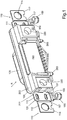
- a Sub-D plug or D-Sub plug in the FIGS. 1 to 4 in isometric view during different manufacturing steps and in Fig. 5 shown obliquely from the front, has a base plate 100 to which a connector housing 200 attached, for example glued or molded, is.
- a connector housing 200 On its front side, an apron 120, which is connected in one piece with the base plate 100 and is known per se, is arranged, which encloses an opening 122 in which the plug contacts, for example spring contact elements or knife contact elements 400, are arranged.
- the plastic connector housing 200 has two lateral openings 220, which serve to receive, for example, screws, bolts or the like for fastening the plug, for example on a housing wall.
- the base plate 100 openings 114 of which in the FIGS. 1 to 4 only one is visible at a time.
- the other opening 115 is arranged on the plug front side and is aligned with the opening 220 of the connector housing ( Fig. 5 ).
- the side flaps 110 of the base plate 100 are divided into two parts, a first part 111 and a second part 112. Between these parts 111, 112, a bead 117 is arranged, which serve in the following to be described in more detail defined deflection of the parts 111, 112 of the side flaps 110 of the base plate 100.
- a positioning pin 165 which serves to position the plug on the printed circuit board in a manner known per se, is arranged on its lower edge facing a printed circuit board (not shown) via a connecting web 160. In a corresponding manner, the connector plastic housing positioning 265 on.
- Fig. 1 now shows the beginning of the manufacturing process of such a connector, in which the connector housing 200 is already attached to the base plate 100.
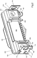
- the two tabs 110 are initially in the non-bent state laterally over the connector housing 200 via.
- a first manufacturing step shown in Fig. 2 .
- the two tabs 110 are first bent by 90 °, so that the part 111 rests against the connector housing 200.
- beads 131 may be provided for this purpose in the part 111, which engage in corresponding recesses 231 of the connector housing and insofar mediate stabilization and / or attachment of the part 111 to the connector housing 200.
- the positioning pin 165 When bending the part 111, the positioning pin 165 is simultaneously brought into position, wherein the connecting web 160, on which the positioning pin 165 is integrally connected to the base plate 100, parallel to the insertion direction, indicated by an arrow R in Fig. 1 , is positioned.
- This design has the great advantage that a bending of the positioning pin 165 in the plugging direction is practically impossible.
- the stability is substantially higher than if the connecting web 160, to which the positioning pin 165 is fastened, would run in the direction of insertion, for example as in FIG Fig. 1 represented, as is the case with connectors from the prior art.
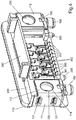
- contact elements 300 are arranged, which are formed on their plug front side, for example, as a blade contact elements or as spring contact elements in a known per se.
- these contact elements 300 are formed as SMD contact elements, that is to say contact elements which can be mounted in surface mounting technology on a printed circuit board.
- the entire plug has a very compact, in particular narrow, structure, so that it can be attached to the edge of a printed circuit board.
- the contact elements 300 of the plug are visible.
- the contact elements 300 are connected via corresponding connections 301, 302 with knife contact elements or spring contact elements of the sub-D plug arranged one above the other in two rows. For example, there are five contact elements in the upper row and four contact elements in the lower row.
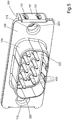
- a plastic bottle 290 is provided on the back of the connector, which is molded, for example, on the connector housing 200. By folding up the tab 290, the contact elements are exposed, by folding down the plastic bottle 290, the contact elements against external influences are not only protected, but also insulated.
- the above-described connector is characterized by a simple construction and especially by a simple production.
Landscapes
- Details Of Connecting Devices For Male And Female Coupling (AREA)
- Coupling Device And Connection With Printed Circuit (AREA)
- Manufacturing Of Electrical Connectors (AREA)
Applications Claiming Priority (2)
| Application Number | Priority Date | Filing Date | Title |
|---|---|---|---|
| DE102011107768.9A DE102011107768B4 (de) | 2011-07-15 | 2011-07-15 | Stecker und Verfahren zu seiner Herstellung |
| PCT/DE2012/000686 WO2013010525A1 (de) | 2011-07-15 | 2012-07-10 | Stecker und verfahren zu seiner herstellung |
Publications (2)
| Publication Number | Publication Date |
|---|---|
| EP2732509A1 EP2732509A1 (de) | 2014-05-21 |
| EP2732509B1 true EP2732509B1 (de) | 2017-05-31 |
Family
ID=46967873
Family Applications (1)
| Application Number | Title | Priority Date | Filing Date |
|---|---|---|---|
| EP12766857.2A Not-in-force EP2732509B1 (de) | 2011-07-15 | 2012-07-10 | Stecker und verfahren zu seiner herstellung |
Country Status (9)
| Country | Link |
|---|---|
| US (1) | US9065206B2 (ko) |
| EP (1) | EP2732509B1 (ko) |
| JP (2) | JP2014523098A (ko) |
| KR (1) | KR20140044900A (ko) |
| CN (1) | CN103843204B (ko) |
| DE (1) | DE102011107768B4 (ko) |
| DK (1) | DK2732509T3 (ko) |
| ES (1) | ES2635723T3 (ko) |
| WO (1) | WO2013010525A1 (ko) |
Families Citing this family (4)
| Publication number | Priority date | Publication date | Assignee | Title |
|---|---|---|---|---|
| JP6647825B2 (ja) * | 2015-09-29 | 2020-02-14 | 日本航空電子工業株式会社 | コネクタ及びコネクタ組立体 |
| WO2018080181A1 (ko) * | 2016-10-26 | 2018-05-03 | 삼성에스디아이 주식회사 | 인쇄 회로 기판용 커넥터 및 인쇄 회로 기판과 커넥터를 포함한 전지 시스템 |
| DE102017106036B3 (de) * | 2017-03-21 | 2018-09-13 | Harting Electric Gmbh & Co. Kg | Halterahmen mit PE-Kontakt |
| US11258198B1 (en) * | 2018-07-06 | 2022-02-22 | New Concepts Development Corporation | Peripheral cord lock |
Family Cites Families (18)
| Publication number | Priority date | Publication date | Assignee | Title |
|---|---|---|---|---|
| US4518209A (en) * | 1983-06-30 | 1985-05-21 | Welcon Connector Company | Connector block with RF shield |
| JPS6231383U (ko) * | 1985-08-08 | 1987-02-25 | ||
| JPH0436556Y2 (ko) * | 1987-05-18 | 1992-08-28 | ||
| US5314146A (en) | 1992-03-13 | 1994-05-24 | Spectrum Astro, Inc. | Multi-mission spacecraft bus having space frame structural design |
| DE9208703U1 (de) | 1992-06-29 | 1993-10-28 | Siemens Ag | Filter-Steckverbinder mit Schirmgehäuse |
| JP2606080Y2 (ja) * | 1993-02-09 | 2000-09-11 | 住友電装株式会社 | レバー式コネクタ |
| EP0874421B1 (de) * | 1997-04-25 | 2007-06-20 | Tyco Electronics Logistics AG | Sub-D-Stecker in SMD-Technik |
| DE20106408U1 (de) | 2001-04-12 | 2001-06-28 | Festo Ag & Co | Elektrische Steckverbindungseinrichtung |
| DE20305734U1 (de) | 2003-04-03 | 2003-06-12 | Festo Ag & Co | Adapter und damit ausgestattete fluidtechnische Ventilbatterie |
| JP3753706B2 (ja) * | 2003-05-22 | 2006-03-08 | 日本航空電子工業株式会社 | コネクタ |
| JP2005004990A (ja) * | 2003-06-09 | 2005-01-06 | Fujikura Ltd | 圧接端子及び圧接コネクタ |
| DE202006018042U1 (de) | 2006-11-28 | 2007-05-24 | Hengstler Gmbh | Dichtung für Flanschsteckerverbinder |
| JP5008492B2 (ja) * | 2007-08-01 | 2012-08-22 | 株式会社オートネットワーク技術研究所 | シールドコネクタ |
| DE202008016738U1 (de) | 2008-12-18 | 2009-03-26 | Harting Electronics Gmbh & Co. Kg | Geschirmter Steckverbinder |
| CN201498649U (zh) | 2009-06-02 | 2010-06-02 | 富士康(昆山)电脑接插件有限公司 | 电连接器 |
| CN201498677U (zh) * | 2009-09-04 | 2010-06-02 | 富士康(昆山)电脑接插件有限公司 | 电连接器 |
| JP5066243B2 (ja) * | 2010-06-08 | 2012-11-07 | ヒロセ電機株式会社 | 電気コネクタ、およびツイストペアケーブルと電気コネクタとの接続方法 |
| US20130045631A1 (en) * | 2011-08-16 | 2013-02-21 | Cheng Uei Precision Industry Co., Ltd. | Socket connector |
-
2011
- 2011-07-15 DE DE102011107768.9A patent/DE102011107768B4/de not_active Expired - Fee Related
-
2012
- 2012-07-10 WO PCT/DE2012/000686 patent/WO2013010525A1/de active Application Filing
- 2012-07-10 US US14/232,680 patent/US9065206B2/en not_active Expired - Fee Related
- 2012-07-10 EP EP12766857.2A patent/EP2732509B1/de not_active Not-in-force
- 2012-07-10 ES ES12766857.2T patent/ES2635723T3/es active Active
- 2012-07-10 DK DK12766857.2T patent/DK2732509T3/en active
- 2012-07-10 CN CN201280040323.2A patent/CN103843204B/zh not_active Expired - Fee Related
- 2012-07-10 KR KR1020147003208A patent/KR20140044900A/ko not_active Application Discontinuation
- 2012-07-10 JP JP2014520536A patent/JP2014523098A/ja active Pending
-
2016
- 2016-08-04 JP JP2016003814U patent/JP3207512U/ja not_active Expired - Fee Related
Also Published As
| Publication number | Publication date |
|---|---|
| US9065206B2 (en) | 2015-06-23 |
| ES2635723T3 (es) | 2017-10-04 |
| JP2014523098A (ja) | 2014-09-08 |
| DE102011107768B4 (de) | 2015-04-09 |
| DK2732509T3 (en) | 2017-07-31 |
| DE102011107768A1 (de) | 2013-01-17 |
| JP3207512U (ja) | 2016-11-17 |
| CN103843204B (zh) | 2016-05-11 |
| CN103843204A (zh) | 2014-06-04 |
| KR20140044900A (ko) | 2014-04-15 |
| WO2013010525A4 (de) | 2013-03-21 |
| EP2732509A1 (de) | 2014-05-21 |
| US20140220810A1 (en) | 2014-08-07 |
| WO2013010525A1 (de) | 2013-01-24 |
Similar Documents
| Publication | Publication Date | Title |
|---|---|---|
| DE19736607C1 (de) | Leiterplattensteckbuchse | |
| EP0748486A1 (de) | Steckkarte für elektronische datenverarbeitungsgeräte und verfahren zu dessen herstellung und montage | |
| DE2053568A1 (de) | Anschlußbuchsen fur integrierte Schaltungen und Verfahren zur gleich zeitigen Montage mehrerer Buchsen | |
| EP2959546B1 (de) | Kontaktträger mit einem toleranzausgleichabschnitt | |
| DE112010004545T5 (de) | Stecker zum Anbringen eines Elektrolytkondensators auf eine Platte und elektronische Schaltungsvorrichtung | |
| DE112012000474T5 (de) | Platinenverbindungsanschluss | |
| DE10119695B4 (de) | Steckverbinder für elektronische Bauelemente | |
| DE3436119C2 (de) | Kontaktfederelement zum Kontaktieren von Leiterplatten | |
| EP2732509B1 (de) | Stecker und verfahren zu seiner herstellung | |
| DE112008001092T5 (de) | Schutzabdeckung für einen Schaltungsträger | |
| DE102005042131A1 (de) | Abschirmgehäuse mit Einpresspins sowie Verfahren zu dessen Herstellung | |
| DE4310369A1 (de) | Adapter | |
| EP2200125B1 (de) | Geschirmter Steckverbinder | |
| EP2305010B1 (de) | Elektrische schaltungsanordnung | |
| DE202008014542U1 (de) | Steckverbinder für Schaltungsplatinen | |
| DE102016002821A1 (de) | Schaltkreis einer elektronischen Steuereinheit | |
| DE102018000204A1 (de) | Steckverbinderanordnung | |
| DE102016107898A1 (de) | Laterale Leiterplattenverbindung | |
| DE202011103356U1 (de) | Stecker | |
| EP2709212B1 (de) | Anordnung zum Verbinden von Leiterplatten | |
| DE10318980A1 (de) | Steckverbinder zur elektrischen Verbindung elektronischer Komponenten | |
| DE102016120180B4 (de) | Leiterplatten- und Mehrfachklemme | |
| DE102012212274B4 (de) | Elektrischer Stecker mit Abdichtung und Verfahren zur Herstellung des elektrischen Steckers | |
| DE102017212602A1 (de) | Steuergerät und elektrische Verbindungsanordnung | |
| DE102010019020A1 (de) | Stapelbare Klemmträgerelemente für Flachbaugruppen |
Legal Events
| Date | Code | Title | Description |
|---|---|---|---|
| PUAI | Public reference made under article 153(3) epc to a published international application that has entered the european phase |
Free format text: ORIGINAL CODE: 0009012 |
|
| 17P | Request for examination filed |
Effective date: 20140211 |
|
| AK | Designated contracting states |
Kind code of ref document: A1 Designated state(s): AL AT BE BG CH CY CZ DE DK EE ES FI FR GB GR HR HU IE IS IT LI LT LU LV MC MK MT NL NO PL PT RO RS SE SI SK SM TR |
|
| DAX | Request for extension of the european patent (deleted) | ||
| GRAP | Despatch of communication of intention to grant a patent |
Free format text: ORIGINAL CODE: EPIDOSNIGR1 |
|
| INTG | Intention to grant announced |
Effective date: 20170201 |
|
| GRAS | Grant fee paid |
Free format text: ORIGINAL CODE: EPIDOSNIGR3 |
|
| GRAA | (expected) grant |
Free format text: ORIGINAL CODE: 0009210 |
|
| AK | Designated contracting states |
Kind code of ref document: B1 Designated state(s): AL AT BE BG CH CY CZ DE DK EE ES FI FR GB GR HR HU IE IS IT LI LT LU LV MC MK MT NL NO PL PT RO RS SE SI SK SM TR |
|
| REG | Reference to a national code |
Ref country code: CH Ref legal event code: EP Ref country code: GB Ref legal event code: FG4D Free format text: NOT ENGLISH |
|
| REG | Reference to a national code |
Ref country code: AT Ref legal event code: REF Ref document number: 898217 Country of ref document: AT Kind code of ref document: T Effective date: 20170615 |
|
| REG | Reference to a national code |
Ref country code: IE Ref legal event code: FG4D Free format text: LANGUAGE OF EP DOCUMENT: GERMAN |
|
| REG | Reference to a national code |
Ref country code: DE Ref legal event code: R096 Ref document number: 502012010455 Country of ref document: DE |
|
| REG | Reference to a national code |
Ref country code: FR Ref legal event code: PLFP Year of fee payment: 6 |
|
| REG | Reference to a national code |
Ref country code: CH Ref legal event code: NV Representative=s name: RENTSCH PARTNER AG, CH Ref country code: DK Ref legal event code: T3 Effective date: 20170728 |
|
| REG | Reference to a national code |
Ref country code: SE Ref legal event code: TRGR |
|
| REG | Reference to a national code |
Ref country code: NL Ref legal event code: FP |
|
| REG | Reference to a national code |
Ref country code: CH Ref legal event code: PCAR Free format text: NEW ADDRESS: BELLERIVESTRASSE 203 POSTFACH, 8034 ZUERICH (CH) |
|
| REG | Reference to a national code |
Ref country code: ES Ref legal event code: FG2A Ref document number: 2635723 Country of ref document: ES Kind code of ref document: T3 Effective date: 20171004 |
|
| REG | Reference to a national code |
Ref country code: LT Ref legal event code: MG4D |
|
| REG | Reference to a national code |
Ref country code: NO Ref legal event code: T2 Effective date: 20170531 |
|
| PG25 | Lapsed in a contracting state [announced via postgrant information from national office to epo] |
Ref country code: GR Free format text: LAPSE BECAUSE OF FAILURE TO SUBMIT A TRANSLATION OF THE DESCRIPTION OR TO PAY THE FEE WITHIN THE PRESCRIBED TIME-LIMIT Effective date: 20170901 Ref country code: HR Free format text: LAPSE BECAUSE OF FAILURE TO SUBMIT A TRANSLATION OF THE DESCRIPTION OR TO PAY THE FEE WITHIN THE PRESCRIBED TIME-LIMIT Effective date: 20170531 Ref country code: LT Free format text: LAPSE BECAUSE OF FAILURE TO SUBMIT A TRANSLATION OF THE DESCRIPTION OR TO PAY THE FEE WITHIN THE PRESCRIBED TIME-LIMIT Effective date: 20170531 |
|
| PG25 | Lapsed in a contracting state [announced via postgrant information from national office to epo] |
Ref country code: RS Free format text: LAPSE BECAUSE OF FAILURE TO SUBMIT A TRANSLATION OF THE DESCRIPTION OR TO PAY THE FEE WITHIN THE PRESCRIBED TIME-LIMIT Effective date: 20170531 Ref country code: IS Free format text: LAPSE BECAUSE OF FAILURE TO SUBMIT A TRANSLATION OF THE DESCRIPTION OR TO PAY THE FEE WITHIN THE PRESCRIBED TIME-LIMIT Effective date: 20170930 Ref country code: BG Free format text: LAPSE BECAUSE OF FAILURE TO SUBMIT A TRANSLATION OF THE DESCRIPTION OR TO PAY THE FEE WITHIN THE PRESCRIBED TIME-LIMIT Effective date: 20170831 Ref country code: LV Free format text: LAPSE BECAUSE OF FAILURE TO SUBMIT A TRANSLATION OF THE DESCRIPTION OR TO PAY THE FEE WITHIN THE PRESCRIBED TIME-LIMIT Effective date: 20170531 |
|
| PG25 | Lapsed in a contracting state [announced via postgrant information from national office to epo] |
Ref country code: SK Free format text: LAPSE BECAUSE OF FAILURE TO SUBMIT A TRANSLATION OF THE DESCRIPTION OR TO PAY THE FEE WITHIN THE PRESCRIBED TIME-LIMIT Effective date: 20170531 Ref country code: CZ Free format text: LAPSE BECAUSE OF FAILURE TO SUBMIT A TRANSLATION OF THE DESCRIPTION OR TO PAY THE FEE WITHIN THE PRESCRIBED TIME-LIMIT Effective date: 20170531 Ref country code: EE Free format text: LAPSE BECAUSE OF FAILURE TO SUBMIT A TRANSLATION OF THE DESCRIPTION OR TO PAY THE FEE WITHIN THE PRESCRIBED TIME-LIMIT Effective date: 20170531 Ref country code: RO Free format text: LAPSE BECAUSE OF FAILURE TO SUBMIT A TRANSLATION OF THE DESCRIPTION OR TO PAY THE FEE WITHIN THE PRESCRIBED TIME-LIMIT Effective date: 20170531 |
|
| PG25 | Lapsed in a contracting state [announced via postgrant information from national office to epo] |
Ref country code: PL Free format text: LAPSE BECAUSE OF FAILURE TO SUBMIT A TRANSLATION OF THE DESCRIPTION OR TO PAY THE FEE WITHIN THE PRESCRIBED TIME-LIMIT Effective date: 20170531 Ref country code: SM Free format text: LAPSE BECAUSE OF FAILURE TO SUBMIT A TRANSLATION OF THE DESCRIPTION OR TO PAY THE FEE WITHIN THE PRESCRIBED TIME-LIMIT Effective date: 20170531 |
|
| REG | Reference to a national code |
Ref country code: DE Ref legal event code: R097 Ref document number: 502012010455 Country of ref document: DE |
|
| PLBE | No opposition filed within time limit |
Free format text: ORIGINAL CODE: 0009261 |
|
| STAA | Information on the status of an ep patent application or granted ep patent |
Free format text: STATUS: NO OPPOSITION FILED WITHIN TIME LIMIT |
|
| 26N | No opposition filed |
Effective date: 20180301 |
|
| PG25 | Lapsed in a contracting state [announced via postgrant information from national office to epo] |
Ref country code: SI Free format text: LAPSE BECAUSE OF FAILURE TO SUBMIT A TRANSLATION OF THE DESCRIPTION OR TO PAY THE FEE WITHIN THE PRESCRIBED TIME-LIMIT Effective date: 20170531 |
|
| PG25 | Lapsed in a contracting state [announced via postgrant information from national office to epo] |
Ref country code: LU Free format text: LAPSE BECAUSE OF NON-PAYMENT OF DUE FEES Effective date: 20170710 |
|
| REG | Reference to a national code |
Ref country code: FR Ref legal event code: PLFP Year of fee payment: 7 |
|
| PG25 | Lapsed in a contracting state [announced via postgrant information from national office to epo] |
Ref country code: MT Free format text: LAPSE BECAUSE OF FAILURE TO SUBMIT A TRANSLATION OF THE DESCRIPTION OR TO PAY THE FEE WITHIN THE PRESCRIBED TIME-LIMIT Effective date: 20170531 |
|
| PG25 | Lapsed in a contracting state [announced via postgrant information from national office to epo] |
Ref country code: MC Free format text: LAPSE BECAUSE OF FAILURE TO SUBMIT A TRANSLATION OF THE DESCRIPTION OR TO PAY THE FEE WITHIN THE PRESCRIBED TIME-LIMIT Effective date: 20170531 Ref country code: HU Free format text: LAPSE BECAUSE OF FAILURE TO SUBMIT A TRANSLATION OF THE DESCRIPTION OR TO PAY THE FEE WITHIN THE PRESCRIBED TIME-LIMIT; INVALID AB INITIO Effective date: 20120710 |
|
| PG25 | Lapsed in a contracting state [announced via postgrant information from national office to epo] |
Ref country code: CY Free format text: LAPSE BECAUSE OF NON-PAYMENT OF DUE FEES Effective date: 20170531 |
|
| PG25 | Lapsed in a contracting state [announced via postgrant information from national office to epo] |
Ref country code: MK Free format text: LAPSE BECAUSE OF FAILURE TO SUBMIT A TRANSLATION OF THE DESCRIPTION OR TO PAY THE FEE WITHIN THE PRESCRIBED TIME-LIMIT Effective date: 20170531 |
|
| PG25 | Lapsed in a contracting state [announced via postgrant information from national office to epo] |
Ref country code: TR Free format text: LAPSE BECAUSE OF FAILURE TO SUBMIT A TRANSLATION OF THE DESCRIPTION OR TO PAY THE FEE WITHIN THE PRESCRIBED TIME-LIMIT Effective date: 20170531 |
|
| PG25 | Lapsed in a contracting state [announced via postgrant information from national office to epo] |
Ref country code: PT Free format text: LAPSE BECAUSE OF FAILURE TO SUBMIT A TRANSLATION OF THE DESCRIPTION OR TO PAY THE FEE WITHIN THE PRESCRIBED TIME-LIMIT Effective date: 20170531 |
|
| PG25 | Lapsed in a contracting state [announced via postgrant information from national office to epo] |
Ref country code: AL Free format text: LAPSE BECAUSE OF FAILURE TO SUBMIT A TRANSLATION OF THE DESCRIPTION OR TO PAY THE FEE WITHIN THE PRESCRIBED TIME-LIMIT Effective date: 20170531 |
|
| PGFP | Annual fee paid to national office [announced via postgrant information from national office to epo] |
Ref country code: NL Payment date: 20200729 Year of fee payment: 9 |
|
| PGFP | Annual fee paid to national office [announced via postgrant information from national office to epo] |
Ref country code: ES Payment date: 20200818 Year of fee payment: 9 Ref country code: FR Payment date: 20200727 Year of fee payment: 9 Ref country code: GB Payment date: 20200724 Year of fee payment: 9 Ref country code: DK Payment date: 20200722 Year of fee payment: 9 Ref country code: FI Payment date: 20200720 Year of fee payment: 9 Ref country code: IE Payment date: 20200717 Year of fee payment: 9 Ref country code: NO Payment date: 20200722 Year of fee payment: 9 Ref country code: DE Payment date: 20200728 Year of fee payment: 9 |
|
| PGFP | Annual fee paid to national office [announced via postgrant information from national office to epo] |
Ref country code: AT Payment date: 20200720 Year of fee payment: 9 Ref country code: BE Payment date: 20200722 Year of fee payment: 9 Ref country code: CH Payment date: 20200724 Year of fee payment: 9 Ref country code: SE Payment date: 20200724 Year of fee payment: 9 Ref country code: IT Payment date: 20200731 Year of fee payment: 9 |
|
| REG | Reference to a national code |
Ref country code: DE Ref legal event code: R119 Ref document number: 502012010455 Country of ref document: DE |
|
| REG | Reference to a national code |
Ref country code: DK Ref legal event code: EBP Effective date: 20210731 |
|
| REG | Reference to a national code |
Ref country code: FI Ref legal event code: MAE Ref country code: CH Ref legal event code: PL Ref country code: NO Ref legal event code: MMEP |
|
| REG | Reference to a national code |
Ref country code: NL Ref legal event code: MM Effective date: 20210801 |
|
| REG | Reference to a national code |
Ref country code: AT Ref legal event code: MM01 Ref document number: 898217 Country of ref document: AT Kind code of ref document: T Effective date: 20210710 |
|
| GBPC | Gb: european patent ceased through non-payment of renewal fee |
Effective date: 20210710 |
|
| REG | Reference to a national code |
Ref country code: BE Ref legal event code: MM Effective date: 20210731 |
|
| PG25 | Lapsed in a contracting state [announced via postgrant information from national office to epo] |
Ref country code: LI Free format text: LAPSE BECAUSE OF NON-PAYMENT OF DUE FEES Effective date: 20210731 Ref country code: GB Free format text: LAPSE BECAUSE OF NON-PAYMENT OF DUE FEES Effective date: 20210710 Ref country code: FI Free format text: LAPSE BECAUSE OF NON-PAYMENT OF DUE FEES Effective date: 20210710 Ref country code: DE Free format text: LAPSE BECAUSE OF NON-PAYMENT OF DUE FEES Effective date: 20220201 Ref country code: CH Free format text: LAPSE BECAUSE OF NON-PAYMENT OF DUE FEES Effective date: 20210731 Ref country code: AT Free format text: LAPSE BECAUSE OF NON-PAYMENT OF DUE FEES Effective date: 20210710 |
|
| PG25 | Lapsed in a contracting state [announced via postgrant information from national office to epo] |
Ref country code: SE Free format text: LAPSE BECAUSE OF NON-PAYMENT OF DUE FEES Effective date: 20210711 Ref country code: NO Free format text: LAPSE BECAUSE OF NON-PAYMENT OF DUE FEES Effective date: 20210731 Ref country code: NL Free format text: LAPSE BECAUSE OF NON-PAYMENT OF DUE FEES Effective date: 20210801 Ref country code: FR Free format text: LAPSE BECAUSE OF NON-PAYMENT OF DUE FEES Effective date: 20210731 |
|
| PG25 | Lapsed in a contracting state [announced via postgrant information from national office to epo] |
Ref country code: IT Free format text: LAPSE BECAUSE OF NON-PAYMENT OF DUE FEES Effective date: 20210710 Ref country code: IE Free format text: LAPSE BECAUSE OF NON-PAYMENT OF DUE FEES Effective date: 20210710 Ref country code: DK Free format text: LAPSE BECAUSE OF NON-PAYMENT OF DUE FEES Effective date: 20210731 Ref country code: BE Free format text: LAPSE BECAUSE OF NON-PAYMENT OF DUE FEES Effective date: 20210731 |
|
| REG | Reference to a national code |
Ref country code: ES Ref legal event code: FD2A Effective date: 20220926 |
|
| PG25 | Lapsed in a contracting state [announced via postgrant information from national office to epo] |
Ref country code: ES Free format text: LAPSE BECAUSE OF NON-PAYMENT OF DUE FEES Effective date: 20210711 |