EP2700965A2 - Dispositif semi-conducteur et dispositif de surveillance de tension de batterie - Google Patents
Dispositif semi-conducteur et dispositif de surveillance de tension de batterie Download PDFInfo
- Publication number
- EP2700965A2 EP2700965A2 EP13179215.2A EP13179215A EP2700965A2 EP 2700965 A2 EP2700965 A2 EP 2700965A2 EP 13179215 A EP13179215 A EP 13179215A EP 2700965 A2 EP2700965 A2 EP 2700965A2
- Authority
- EP
- European Patent Office
- Prior art keywords
- voltage
- potential
- terminal
- low
- current
- Prior art date
- Legal status (The legal status is an assumption and is not a legal conclusion. Google has not performed a legal analysis and makes no representation as to the accuracy of the status listed.)
- Granted
Links
- 239000004065 semiconductor Substances 0.000 title claims abstract description 78
- 238000012806 monitoring device Methods 0.000 title claims description 28
- 238000005259 measurement Methods 0.000 claims abstract description 50
- 238000006243 chemical reaction Methods 0.000 claims description 18
- 238000004891 communication Methods 0.000 claims description 15
- 238000012544 monitoring process Methods 0.000 abstract description 89
- 238000001514 detection method Methods 0.000 abstract description 69
- 239000000758 substrate Substances 0.000 abstract description 12
- 238000010586 diagram Methods 0.000 description 13
- 238000000034 method Methods 0.000 description 11
- 238000007599 discharging Methods 0.000 description 10
- HBBGRARXTFLTSG-UHFFFAOYSA-N Lithium ion Chemical compound [Li+] HBBGRARXTFLTSG-UHFFFAOYSA-N 0.000 description 6
- 229910001416 lithium ion Inorganic materials 0.000 description 6
- 230000002159 abnormal effect Effects 0.000 description 5
- 230000005856 abnormality Effects 0.000 description 5
- 230000005540 biological transmission Effects 0.000 description 5
- 230000003071 parasitic effect Effects 0.000 description 5
- 230000008878 coupling Effects 0.000 description 4
- 238000010168 coupling process Methods 0.000 description 4
- 238000005859 coupling reaction Methods 0.000 description 4
- 230000010354 integration Effects 0.000 description 4
- 239000003990 capacitor Substances 0.000 description 3
- 230000009977 dual effect Effects 0.000 description 2
- 238000012986 modification Methods 0.000 description 2
- 230000004048 modification Effects 0.000 description 2
- 230000009471 action Effects 0.000 description 1
- 230000008901 benefit Effects 0.000 description 1
- 230000008859 change Effects 0.000 description 1
- 238000013461 design Methods 0.000 description 1
- 238000003745 diagnosis Methods 0.000 description 1
- 230000000694 effects Effects 0.000 description 1
- 230000001747 exhibiting effect Effects 0.000 description 1
- 238000004880 explosion Methods 0.000 description 1
- 239000000446 fuel Substances 0.000 description 1
- 229910052739 hydrogen Inorganic materials 0.000 description 1
- 239000001257 hydrogen Substances 0.000 description 1
- 230000002093 peripheral effect Effects 0.000 description 1
- 230000008569 process Effects 0.000 description 1
- 230000009467 reduction Effects 0.000 description 1
- 230000004044 response Effects 0.000 description 1
- 238000004092 self-diagnosis Methods 0.000 description 1
- 230000008719 thickening Effects 0.000 description 1
Images


Classifications
-
- H—ELECTRICITY
- H02—GENERATION; CONVERSION OR DISTRIBUTION OF ELECTRIC POWER
- H02J—CIRCUIT ARRANGEMENTS OR SYSTEMS FOR SUPPLYING OR DISTRIBUTING ELECTRIC POWER; SYSTEMS FOR STORING ELECTRIC ENERGY
- H02J7/00—Circuit arrangements for charging or depolarising batteries or for supplying loads from batteries
- H02J7/0047—Circuit arrangements for charging or depolarising batteries or for supplying loads from batteries with monitoring or indicating devices or circuits
- H02J7/0048—Detection of remaining charge capacity or state of charge [SOC]
-
- G—PHYSICS
- G01—MEASURING; TESTING
- G01R—MEASURING ELECTRIC VARIABLES; MEASURING MAGNETIC VARIABLES
- G01R31/00—Arrangements for testing electric properties; Arrangements for locating electric faults; Arrangements for electrical testing characterised by what is being tested not provided for elsewhere
- G01R31/36—Arrangements for testing, measuring or monitoring the electrical condition of accumulators or electric batteries, e.g. capacity or state of charge [SoC]
- G01R31/382—Arrangements for monitoring battery or accumulator variables, e.g. SoC
- G01R31/3835—Arrangements for monitoring battery or accumulator variables, e.g. SoC involving only voltage measurements
-
- G—PHYSICS
- G01—MEASURING; TESTING
- G01R—MEASURING ELECTRIC VARIABLES; MEASURING MAGNETIC VARIABLES
- G01R31/00—Arrangements for testing electric properties; Arrangements for locating electric faults; Arrangements for electrical testing characterised by what is being tested not provided for elsewhere
- G01R31/36—Arrangements for testing, measuring or monitoring the electrical condition of accumulators or electric batteries, e.g. capacity or state of charge [SoC]
- G01R31/396—Acquisition or processing of data for testing or for monitoring individual cells or groups of cells within a battery
-
- H—ELECTRICITY
- H02—GENERATION; CONVERSION OR DISTRIBUTION OF ELECTRIC POWER
- H02H—EMERGENCY PROTECTIVE CIRCUIT ARRANGEMENTS
- H02H7/00—Emergency protective circuit arrangements specially adapted for specific types of electric machines or apparatus or for sectionalised protection of cable or line systems, and effecting automatic switching in the event of an undesired change from normal working conditions
- H02H7/18—Emergency protective circuit arrangements specially adapted for specific types of electric machines or apparatus or for sectionalised protection of cable or line systems, and effecting automatic switching in the event of an undesired change from normal working conditions for batteries; for accumulators
-
- H—ELECTRICITY
- H02—GENERATION; CONVERSION OR DISTRIBUTION OF ELECTRIC POWER
- H02J—CIRCUIT ARRANGEMENTS OR SYSTEMS FOR SUPPLYING OR DISTRIBUTING ELECTRIC POWER; SYSTEMS FOR STORING ELECTRIC ENERGY
- H02J7/00—Circuit arrangements for charging or depolarising batteries or for supplying loads from batteries
- H02J7/0013—Circuit arrangements for charging or depolarising batteries or for supplying loads from batteries acting upon several batteries simultaneously or sequentially
- H02J7/0014—Circuits for equalisation of charge between batteries
- H02J7/0016—Circuits for equalisation of charge between batteries using shunting, discharge or bypass circuits
-
- G—PHYSICS
- G01—MEASURING; TESTING
- G01R—MEASURING ELECTRIC VARIABLES; MEASURING MAGNETIC VARIABLES
- G01R19/00—Arrangements for measuring currents or voltages or for indicating presence or sign thereof
- G01R19/165—Indicating that current or voltage is either above or below a predetermined value or within or outside a predetermined range of values
- G01R19/16533—Indicating that current or voltage is either above or below a predetermined value or within or outside a predetermined range of values characterised by the application
- G01R19/16538—Indicating that current or voltage is either above or below a predetermined value or within or outside a predetermined range of values characterised by the application in AC or DC supplies
- G01R19/16542—Indicating that current or voltage is either above or below a predetermined value or within or outside a predetermined range of values characterised by the application in AC or DC supplies for batteries
Definitions
- the present invention relates to a device which measures a voltage of each of plural voltage supplies coupled in series and collects the measurement results, and, in particular, the present invention can be utilized suitably for a semiconductor device which configures the device.
- an electric vehicle which employs a motor as a driving source for traveling of the vehicle is developed by not only automakers but other companies or groups.
- an in-vehicle power supply which produces a high voltage of several hundred volts is required.
- This power source is realized by a battery system comprised of a series coupling of many unit cells (battery cells) each of which produces a voltage of several volts.
- Such a battery system needs to measure the voltage of each of plural unit cells coupled in series with high accuracy, in order to determine the state of the battery (for example, an overcharge state, an overdischarge state, the remaining amount of charge) under all environments including at the time of traveling and electric charging of a vehicle.
- a battery system may incur serious risks, such as ignition and explosion, at the time of occurrence of abnormal conditions; therefore, in order to operate the battery system safely, a fail-safe solution is adopted in the voltage measurement device.
- a battery control system is usually comprised of a supervisory IC (Integrated Circuit), a fault monitor IC (secondary protection IC), an MCU (Micro Controller Unit), and others.
- the supervisory IC monitors the state of a battery cell and outputs state data (mainly battery voltage).
- the supervisory IC is provided with an analog-to-digital converter circuit (ADC), measures the battery voltage of a unit cell to an accuracy of about 5 mV, and outputs the measurement result in response to an instruction from the MCU.
- ADC analog-to-digital converter circuit
- the fault monitor IC monitors the voltage of a battery cell and outputs an abnormality detection signal when the monitored voltage deviates from a predetermined voltage range.
- the fault monitor IC outputs an abnormality detection signal, noting that it is an overdischarge state when the unit cell voltage becomes less than 2V, and outputs an abnormality detection signal, noting that it is an overcharge state when the unit cell voltage becomes greater than 4.5V.
- the MCU controls the supervisory IC and the secondary protection IC, and at the same time, controls the entire battery control system on the basis of the outputs of the supervisory IC and the fault monitor IC.
- the MCU summarizes the state data outputted from the supervisory IC in real time, and performs suitable control on the basis of the state data.
- severe functional safety standards are applied to a vehicle electronic control system.
- many kinds of diagnosis function are provided in the battery control system.
- the examples include the detection function of disconnection between a node of unit cells of an assembled battery and a terminal of the supervisory IC, and self-diagnosis function of each blocks, such as ADC, etc.
- the fault monitor IC which can detect an overcharge state and an overdischarge state is frequently employed for realizing such functional safety.
- Patent Literature 1 discloses the technique of adding to a supervisory IC the function capable of detecting disconnection between a node of unit cells in an assembled battery and a terminal of the supervisory IC. The disconnection is detected by observing a voltage drop which occurs at the time when the node and the ground is selectively short-circuited with a resistor and a switch. The measurement of the voltage drop is performed by utilizing an ADC provided in the supervisory IC for measurement of the cell voltage as the original function.
- Patent Literature 2 realizes the function of detecting disconnection between a node of unit cells in an assembled battery and a terminal of a supervisory IC, by employing an overvoltage detection comparator and a low-voltage detection comparator. In the normal operation without disconnection, the overvoltage detection comparator determines that an abnormality is detected when a cell voltage becomes greater than a predetermined value, and the low-voltage detection comparator determines that an abnormality is detected when a cell voltage becomes less than a predetermined value.
- Patent Literature 2 points out that "when disconnection occurs in the voltage measurement wiring, it is important to detect the disconnection immediately and to take fail-safe action" (Paragragh 0004).
- Patent Literature 3 discloses an invention which has improved the invention disclosed by Patent Literature 2. Patent Literature 3 solves an issue that an output of a voltage sensor module is accidentally outputted due to disconnection of wiring, thereby causing an unstable output as a battery voltage monitoring device.
- Patent Literature 4 discloses a battery voltage monitoring device which can check whether a comparator for monitoring the occurrence of an overcharge state or an overdischarge state is working properly, in the state where the voltage of each battery cell configuring an assembled battery is in the normal voltage range.
- Patent Literature 1, 2, 3, and 4 The examination performed by the present inventors on Patent Literature 1, 2, 3, and 4 has revealed that there exists the following new issue.
- Patent Literature 1 In the technique disclosed by Patent Literature 1, the supervisory IC detects disconnection between a node of unit cells in an assembled battery and a terminal of the supervisory IC by employing an ADC provided for the measurement of the cell voltage as the original function. Therefore, the measurement system and the fault detection system are not independent (not dual-redundant). Accordingly, it is difficult to satisfy the functional safety standards only with the disclosed technique.
- Patent Literature 1 describes simultaneous use of a double protection IC as a premise.
- Patent Literature 2 and 3 is the technique of additionally imparting the function of detecting disconnection between a node of unit cells in the assembled battery and a terminal of the supervisory IC, to the overcharge/overdischarge detection circuit provided in the fault monitor IC, and is independent of the supervisory IC (dual-redundant). Therefore, the functional safety standards can be satisfied.
- the supervisory IC and the fault monitor IC are mounted in separate chips, and neither description nor suggestion is made about their integration in a single semiconductor chip.
- an overvoltage detection comparator and a low-voltage detection comparator are provided in each of unit battery cells, and no consideration is taken about integration onto a single semiconductor substrate.
- Comparator circuits coupled to battery cells series-coupled in multi-stage operate with respectively different potential, and the potential difference between a comparator circuit of the highest potential and a comparator circuit of the lowest potential may amount to several hundred volts. In that case, it is necessary to insulate each comparator circuit coupled to each battery cell from other battery cells; accordingly, it is necessary to adopt multi-well structure in a CMOS process, for example. Even if the multi-well structure is adopted, it is necessary to provide a broad insulating region in order to make a withstand voltage high; therefore, the burden with respect to cost is heavy.
- Patent Literature 4 discloses the technique in which the potential of a node of unit cells is converted by level shifter circuits 12 - 14 and transmitted to a comparator circuit, as illustrated in FIG. 1 for example. However, any concrete realization method of the level shifter circuit is not disclosed.
- the technique disclosed by Patent Literature 4 relates to a failure detection circuit of a comparator which performs overcharge/overdischarge detection; however, there is no reference to the function of detecting disconnection between a node of unit cells and a terminal of the supervisory IC, and, furthermore, there is neither description nor suggestion about integration with the supervisory IC.
- a semiconductor device for measuring voltage of each of plural unit cells series-coupled in multi-stage and configuring an assembled battery is configured as follows.
- the semiconductor device is provided with two terminals to be coupled to two nodes which are both electrodes of a unit cell and coupled with other unit cells, and a voltage measurement circuit which measures an inter-terminal voltage between the two terminals.
- the semiconductor device is further provided with a down-convert level shifter circuit which converts the inter-terminal voltage into a low-potential-side inter-terminal voltage on the basis of a ground potential, and a comparator circuit which compares the converted low-potential-side inter-terminal voltage with a predetermined reference voltage.
- the semiconductor device is also provided with an up-convert level shifter circuit which converts the low-potential-side shunt control signal on the basis of the ground potential into a high-potential-side shunt control signal, and a switch which short-circuits the two terminals via a resistor on the basis of the converted high-potential-side shunt control signal.
- a voltage measurement circuit (7) which measures an inter-terminal voltage between the first terminal and the second terminal.
- a first level shifter circuit (2) which converts the inter-terminal voltage into a low-potential-side inter-terminal voltage.
- a comparator circuit (6) which compares the low-potential-side inter-terminal voltage with a predetermined reference voltage (V ref ).
- a first switch (11) which short-circuits the first terminal and the second terminal via a first resistor (21), on the basis of the high-potential-side shunt control signal.
- the present structure while satisfying the functional safety standards with dual-redundancy of the function of battery voltage monitoring and fault monitoring, it is possible to realize the measurement of a battery voltage as well as the detection of overcharge/overdischarge and disconnection between a node of unit cells and a terminal as the function of fault monitoring, in a circuit formed on a single semiconductor substrate.
- the semiconductor device is comprised of the following elements.
- a third level shifter circuit (4) which converts a low-potential-side sense enable signal (EN_L MON ) into a high-potential-side sense enable signal (EN_H MON ).
- a fourth level shifter circuit (5) which converts a low-potential-side cell balance enable signal (EN_L CB ) into a high-potential-side cell balance enable signal (EN_H CB ).
- a third switch (12) which short-circuits the third terminal and the second terminal, on the basis of the high-potential-side cell balance enable signal.
- the first level shifter circuit is provided with a voltage-to-current converter circuit (8) which converts the inter-terminal voltage into a current value corresponding to the inter-terminal voltage, and a current-to-voltage converter circuit (9) which converts the current value into a low-potential-side inter-terminal voltage corresponding to the current value.
- the first level shifter circuit is also provided with a second switch (13) which controls operation of the voltage-to-current converter circuit, on the basis of the high-potential-side sense enable signal, and a fourth switch (14) which controls operation of the voltage-to-current converter circuit, on the basis of the potential of the third terminal, in parallel with the second switch.
- the present structure it is possible to realize, with a circuit formed on a single semiconductor substrate, the fault detection of the switch (12) which discharges a unit cell in order to realize the cell balance function (function to correct the imbalance of the voltage among plural unit cells), while satisfying the functional safety standards with dual-redundancy with the monitoring of a battery voltage.
- the semiconductor device is comprised of the following elements.
- a third level shifter circuit (4) which converts a low-potential-side sense enable signal (EN_L MON ) into a high-potential-side sense enable signal (EN_H MON ).
- a fourth level shifter circuit (5) which converts a low-potential-side cell balance enable signal (EN_L CB ) into a high-potential-side cell balance enable signal (EN_H CB ).
- the first level shifter circuit is provided with a voltage-to-current converter circuit (8) which converts the inter-terminal voltage into a current value corresponding to the inter-terminal voltage, and a current-to-voltage converter circuit (9) which converts the current value into a low-potential-side inter-terminal voltage corresponding to the current value.
- the semiconductor device (1) is provided with a second switch (13) which controls operation of the voltage-to-current converter circuit, on the basis of the high-potential-side sense enable signal, and a fourth switch (14) which controls operation of the voltage-to-current converter circuit, on the basis of the potential of the third terminal, in parallel with the second switch.
- the present structure with a circuit formed in a single semiconductor substrate, it is possible to realize the fault detection of the switch (15, 16) which discharges a unit cell in order to realize the cell balance function, while satisfying the functional safety standards with dual-redundancy with the monitoring of a battery voltage.
- the current-to-voltage converter circuit is comprised of a fourth resistor (24) and a second high withstand voltage FET.
- the fourth resistor is coupled in series with a diode formed between a drain and a short-circuited gate-and-source of the second high withstand voltage FET, and the current-to-voltage converter circuit converts the inputted conversion current into the low-potential-side inter-terminal voltage corresponding to the current value, and outputs the voltage.
- the down-convert level shifter with a high withstand voltage FET.
- the down-convert level shifter by use of a high withstand voltage FET of a withstand voltage lower than the voltage of the assembled battery.
- the voltage-to-current converter circuit and the current-to-voltage converter circuit are configured as follows, respectively.
- the voltage-to-current converter circuit is comprised of a third resistor (23) and a first high withstand voltage bipolar transistor (41).
- a base of the first high withstand voltage bipolar transistor is coupled to the second terminal, the second switch and the third resistor are coupled in series between an emitter of the first high withstand voltage bipolar transistor and the first terminal, and a conversion current of a current value corresponding to the inter-terminal voltage is outputted to a collector of the first high withstand voltage bipolar transistor.
- the down-convert level shifter with a high withstand voltage bipolar transistor.
- the semiconductor device is further provided with a fifth terminal (C n-3 ) to be coupled to a third node which is one electrode of a unit cell different from the unit cell and is coupled to another unit cell in the plural unit cells.
- the first level shifter circuit is comprised of a third high withstand voltage bipolar transistor (43). A base of the third high withstand voltage bipolar transistor is coupled to the fifth terminal, and a collector and an emitter of the third high withstand voltage bipolar transistor are inserted in a signal line which transmits the conversion current between the voltage-to-current converter circuit and the current-to-voltage converter circuit.
- At least one of the second level shifter circuit, the third level shifter circuit, and the fourth level shifter circuit is a circuit which converts a low-potential-side control signal (EN_L TAP , EN_L CB , EN_L MON ) into a high-potential-side control signal (EN_H TAP , EN_H CB , EN_H MON ), and is configured as follows.
- an up-convert level shifter which is appropriate to drive a switch (11, 12, 13) comprised of an n-channel MOSFET (30_7).
- At least one of the second level shifter circuit, the third level shifter circuit, and the fourth level shifter circuit converts the first low-potential-side control signal (EN_L TAP , EN_L CB , EN_L MON ) into the first high-potential-side control signal (EN_H TAP , EN_H CB , EN_H MON ), and the second low-potential-side control signal (EN_L TAP , EN_L CB , EN_L MON ) into the second high-potential-side control signal (EN_H TAP , EN_H CB , EN_H MON ) of a potential lower than the first high-potential-side control signal.
- At least one of the second level shifter circuit, the third level shifter circuit, and the fourth level shifter circuit is provided with the following elements.
- a second high-withstand voltage transistor (34, 44) which controls the first current output on the basis of the second low-potential-side control signal and outputs a third current output.
- the switch (11, 12, 13) comprised of the p-channel MOSFET (30_8) and the switch (11, 12, 13) comprised of the n-channel MOSFET (30_7) are intermingled, it is possible to configure the up-convert level shifter which is appropriate for driving each of the switches. Accordingly, it is possible to design the circuit area of the switch, etc. optimally.
- the present structure it is possible to easily monitor externally the detection result of overcharge/overdischarge and the detection result of disconnection between a node of unit cells and a terminal.
- the comparator circuit is provided with a high-voltage-side comparator circuit (CCOMP12 - CCOMP1) which compares the low-potential-side inter-terminal voltage with a high-voltage-side reference voltage (V ref H), and a low-voltage-side comparator circuit (DCOMP12 - DCOMP1) which compares the low-potential-side inter-terminal voltage with a low-voltage-side reference voltage (V ref L).
- CCOMP12 - CCOMP1 high-voltage-side comparator circuit
- DCOMP12 - DCOMP1 low-voltage-side comparator circuit
- the semiconductor device is provided with a status register (10) which stores comparison results of each of the high-voltage-side comparator circuit and the low-voltage-side comparator circuit.
- the semiconductor device is further provided with a control register (10) which stores at least one of the low-potential-side shunt control signal (EN_L TAP ), the low-potential-side sense enable signal (EN_L MON ), and the low-potential-side cell balance enable signal (EN_L CB ).
- the present structure it is possible to easily monitor externally the detection result of overcharge/overdischarge, the detection result of disconnection between a node of unit cells and a terminal, and the detection result of fault of the switch (15, 16) which discharges a unit cell in order to realize the cell balance function. Also, it is possible to easily control externally the semiconductor device so as to perform such detecting operation.
- the semiconductor device is provided with an interrupt generating circuit (63) which generates an interrupt signal (INTO) on the basis of the comparison results of each of the high-voltage-side comparator circuit and the low-voltage-side comparator circuit.
- an interrupt generating circuit (63) which generates an interrupt signal (INTO) on the basis of the comparison results of each of the high-voltage-side comparator circuit and the low-voltage-side comparator circuit.
- a battery voltage monitoring device is comprised of plural voltage measurement units provided for each group (BC 1 _ 1 - BC 1 _ N , ⁇ , BC M_1 - BC M_N ) of plural unit cells series-coupled in multi-stage and configuring an assembled battery, and a battery system controller (60) coupled to the plural voltage measurement units.
- Each of the plural voltage measurement units is comprised of a semiconductor device (1_1 - 1_M).
- the semiconductor device is provided with the following elements.
- a voltage measurement circuit (7) which measures an inter-terminal voltage between the first terminal and the second terminal.
- a first level shifter circuit (2) which converts the inter-terminal voltage into a low-potential-side inter-terminal voltage.
- a comparator circuit (6) which compares the low-potential-side inter-terminal voltage with a predetermined reference voltage (V ref ).
- a second level shifter circuit (3) which converts a low-potential-side shunt control signal (EN_L TAP ) into a high-potential-side shunt control signal (EN_H TAP ).
- a first switch (11) which short-circuits the first terminal and the second terminal via a first resistor (21), on the basis of the high-potential-side shunt control signal.
- the battery voltage monitoring device in which each of plural voltage measurement units is provided with the semiconductor device which has realized the measurement of a battery voltage as well as the detection of overcharge/overdischarge and disconnection between a node of unit cells and a terminal as the function of fault monitoring, in a circuit formed on a single semiconductor substrate.
- the semiconductor device is comprised of the following elements.
- a third level shifter circuit (4) which converts a low-potential-side sense enable signal (EN_L MON ) into a high-potential-side sense enable signal (EN_H MON ).
- a fourth level shifter circuit (5) which converts a low-potential-side cell balance enable signal (EN_L CB ) into a high-potential-side cell balance enable signal (EN_H CB ).
- a third switch (12) which short-circuits the third terminal and the second terminal, on the basis of the high-potential-side cell balance enable signal.
- the first level shifter circuit is provided with a voltage-to-current converter circuit (8) which converts the inter-terminal voltage into a current value corresponding to the inter-terminal voltage, and a current-to-voltage converter circuit (9) which converts the current value into a low-potential-side inter-terminal voltage corresponding to the current value.
- the first level shifter circuit is provided with a second switch (13) which controls operation of the voltage-to-current converter circuit on the basis of the high-potential-side sense enable signal, and a fourth switch (14) which controls operation of the voltage-to-current converter circuit on the basis of the potential of the third terminal, in parallel with the second switch.
- the battery voltage monitoring device in which each of plural voltage measurement units is provided with the semiconductor device which has realized, in a circuit formed on a single semiconductor substrate, the fault detection of the switch (12) which discharges a unit cell in order to realize the cell balance function (function to correct the imbalance of the voltage among plural unit cells), while satisfying the functional safety standards with dual-redundancy with the monitoring of a battery voltage.
- the semiconductor device is comprised of the following elements.
- a third level shifter circuit (4) which converts a low-potential-side sense enable signal into a high-potential-side sense enable signal.
- a fourth level shifter circuit (5) which converts a low-potential-side cell balance enable signal into a high-potential-side cell balance enable signal.
- a fifth switch (15, 16) which short-circuits the third terminal and the fourth terminal on the basis of the high-potential-side cell balance enable signal.
- the first level shifter circuit is provided with a voltage-to-current converter circuit (8) which converts the inter-terminal voltage into a current value corresponding to the inter-terminal voltage, and a current-to-voltage converter circuit (9) which converts the current value into a low-potential-side inter-terminal voltage corresponding to the current value.
- the first level shifter circuit is provided with a second switch (13) which controls operation of the voltage-to-current converter circuit, on the basis of the high-potential-side sense enable signal, and a fourth switch (14) which controls operation of the voltage-to-current converter circuit on the basis of the potential of the third terminal, in parallel with the second switch.
- the battery voltage monitoring device in which each of plural voltage measurement units is provided with the semiconductor device which has realized, in a circuit formed on a single semiconductor substrate, the fault detection of the switch (15, 16) which discharges a unit cell in order to realize the cell balance function, while satisfying the functional safety standards with dual-redundancy with the monitoring of a battery voltage.
- the comparator circuit is provided with a high-voltage-side comparator circuit (CCOMP12 - CCOMP1) which compares the low-potential-side inter-terminal voltage with a high-voltage-side reference voltage (V ref H), and a low-voltage-side comparator circuit (DCOMP12 - DCOMP1) which compares the low-potential-side inter-terminal voltage with a low-voltage-side reference voltage (V ref L).
- the semiconductor device is further provided with a status register (10) which stores comparison results of each of the high-voltage-side comparator circuit and the low-voltage-side comparator circuit.
- the semiconductor device included in each of the plural voltage measurement units is coupled to the battery system controller via a communication path (61), and the battery system controller enables the status register accessible via the communication path.
- the present structure it is possible to easily monitor, from a battery system controller (60), the detection result of overcharge/overdischarge and the detection result of disconnection between a node of unit cells and a terminal, in the semiconductor device (1_1 - 1_M) of each voltage measurement unit.
- the comparator circuit is provided with a high-voltage-side comparator circuit (CCOMP12 - CCOMP1) which compares the low-potential-side inter-terminal voltage with a high-voltage-side reference voltage (V ref H), and a low-voltage-side comparator circuit (DCOMP12 - DCOMP1) which compares the low-potential-side inter-terminal voltage with a low-voltage-side reference voltage (V ref L).
- CCOMP12 - CCOMP1 high-voltage-side comparator circuit
- DCOMP12 - DCOMP1 low-voltage-side comparator circuit
- the semiconductor device is provided with a status register (10) which stores comparison results of each of the high-voltage-side comparator circuit and the low-voltage-side comparator circuit.
- the semiconductor device is further provided with a control register (10) which stores at least one of the low-potential-side shunt control signal (EN_L TAP ), the low-potential-side sense enable signal (EN_L MON ), and the low-potential-side cell balance enable signal (EN_L CB ).
- the semiconductor device included in each of the plural voltage measurement units is coupled to the battery system controller via a communication path (61), and the battery system controller enables the status register and the control register accessible via the communication path.
- the present structure it is possible to easily monitor, from the battery system controller (60), the detection result of overcharge/overdischarge, the detection result of disconnection between a node of unit cells and a terminal, and the detection result of fault of the switch (15, 16) which discharges a unit cell in order to realize the cell balance function, in the semiconductor device (1_1 - 1_M) of each voltage measurement unit. Furthermore, it is possible to easily control the semiconductor device so as to perform such detecting operation, from the battery system controller (60).
- the semiconductor device is provided with an interrupt generating circuit which generates an interrupt signal (INTO) to the battery system controller, on the basis of the comparison results of each of the high-voltage-side comparator circuit and the low-voltage-side comparator circuit.
- INTO interrupt signal
- the battery system controller (60) can detect occurrence of fault, without monitoring the status register.
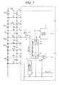
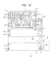
- FIG. 1 illustrates a configuration of principal parts of a battery voltage monitoring IC according to Embodiment 1.
- a battery voltage monitoring IC (a semiconductor device) 1 is for measuring a cell voltage of each of plural unit cells BC 1 - BC 12 which are series-coupled in multi-stage to configure an assembled battery.
- the battery voltage monitoring IC 1 is comprised of terminals C 0 - C 12 coupled to each of nodes coupled in series across both poles of the unit cells BC 1 - BC 12 , and is configured as follows, for example. There exists wiring resistance Rf 0 - Rf 12 between each of the nodes of unit cells BC 1 - BC 12 and each of the terminals C 0 - C 12 , and there also exists parasitic capacitance Cf 0 - Cf 12 between the adjoining pair of the terminals C 0 - C 12 .
- the voltage measurement circuit 7 can be configured by combining a multiplexer MUX and an analog-to-digital converter ADC, for example.
- the multiplexer MUX is comprised of plural switches, selects a signal from the adjoining pair of terminals C n and C n-1 , and transmits it to the analog-to-digital converter ADC.
- the signal from the adjoining pair of terminals C n and C n-1 is a cell voltage of a unit cell BC n .
- the signal is measured by the analog-to-digital converter ADC and the converted digital value is outputted.
- the unit cells BC 1 - BC 12 are selected sequentially, and each cell voltage is measured.
- the analog-to-digital converter ADC may adopt a delta-sigma ADC, a successive-approximation ADC, and others.
- the plural unit cells BC 1 - BC 12 are series-coupled, accordingly, a unit cell located closer to the terminal C 12 has a higher potential, even though the cell voltage for each unit cell is low.
- the potential of the terminal C 12 with reference to the terminal C0 is 44.4V normally but may amount to 50V when all unit cells are in an overcharge state.
- the signal of the terminals C n and C n-1 illustrated in FIG. 1 is equal to the voltage of a unit cell (for example, 3.7V) as the inter-terminal voltage.
- the battery voltage monitoring IC 1 is provided with a down-convert level shifter circuit 2 which converts the inter-terminal voltage between the terminals C n and C n-1 at a high potential side into a low-potential-side inter-terminal voltage, and a comparator circuit 6 which compares the converted low-potential-side inter-terminal voltage with a predetermined reference voltage (V ref ).
- the battery voltage monitoring IC 1 is also provided with an up-convert level shifter circuit 3 which converts a low-potential-side shunt control signal (EN_L TAP ) into a high-potential-side shunt control signal (EN_H TAP ), and a switch 11 which short-circuits the terminals C n and C n-1 via a resistor R TAP 21, on the basis of the converted high-potential-side shunt control signal.
- EN_L TAP low-potential-side shunt control signal
- EN_H TAP high-potential-side shunt control signal
- the switch 11 is opened (set to OFF) and the voltage for each unit cell is measured by the voltage measurement circuit 7.
- the comparator circuit 6 performs overcharge/overdischarge detection by comparing the low-potential-side inter-terminal voltage converted by the down-convert level shifter circuit 2, with a predetermined reference voltage (V ref ). Since others circuits except for the terminals C 0 - C 12 are separated and independent, the measurement of a battery voltage and the overcharge/overdischarge detection as one of the fault monitoring function are provided with dual redundancy.
- the comparator circuit 6 may be comprised of a high-voltage-side comparator circuit which compares the low-potential-side inter-terminal voltage converted by the down-convert level shifter circuit 2 with a high-voltage-side reference voltage (V ref H), and a low-voltage-side comparator circuit which compares the low-potential-side inter-terminal voltage with the low-voltage-side reference voltage (V ref L).
- the high-voltage-side comparator circuit detects the overcharge state, by setting the high-voltage-side reference voltage (V ref H) to 4.5V, and it is possible for the low-voltage-side comparator circuit to detect the overdischarge state, by setting the low-voltage-side reference voltage (V ref L) to 2V.
- the charge stored in the parasitic capacitance Cf n cannot be drawn out, since the monitoring of a battery voltage is configured at high impedance so that a battery may not be consumed as much as possible.
- the potential of the terminal C n tends to be maintained at the midpoint of the terminal C n+1 and the terminal C n-1 by capacitive subdivision of the parasitic capacitance Cf n+1 and Cf n . Accordingly, in order to detect the tap disengagement of the terminal C n , the terminal C n and the terminal C n-1 are short-circuited with the switch 11 via R TAP 21.
- the charge stored in the parasitic capacitance Cf n can be drawn out, and when there exists disconnection, the voltage between the terminal C n and the terminal C n-1 becomes low.
- This voltage is converted into a low-potential-side inter-terminal voltage by the down-convert level shifter circuit 2, and is compared with a predetermined reference voltage V ref by the comparator circuit 6.
- the tap disengagement detection i.e., the detection of disconnection between a node of unit cells and a terminal is performed.
- the down-convert level shifter circuit 2 and the comparator circuit 6 cannot perform concurrently the detection of overcharge/overdischarge and the detection of disconnection between a node of unit cells and a terminal, when they are configured to be shared by the detection of overcharge/overdischarge.
- both kinds of detection are the function of fault monitoring; therefore, when each of them is provided with dual redundancy with the monitoring of a battery voltage, it is possible to satisfy the functional safety standards.
- the detection of overcharge/overdischarge or the detection of disconnection between a node of unit cells and a terminal by use of the down-convert level shifter circuit 2 and the comparator circuit 6 are performed normally.
- the monitoring of a battery voltage can be performed normally.
- the attention is paid to the unit cell BC n , and circuits for measuring the cell voltage of other unit cells are omitted.
- the same circuits are provided in all the terminals. By this means, it is possible to realize the function of the fault monitoring for all the unit cells BC 1 - BC 12 .
- the terminals C 0 - C 12 have mutually different potentials, however, the inter-terminal voltages with different potentials are converted into low-potential-side inter-terminal voltages with the same reference potential by the down-convert level shifter circuit 2.
- the signal EN_H TAP for controlling the switch 11 is assigned with a different potential for every unit cell. Therefore, the up-convert level shifter circuit 3 performs the up-convert level shift which assigns a suitable potential to the low-potential-side shunt control signal EN_H TAP .
- the inter-terminal voltage is level-shifted to the low potential side; therefore, it is possible to configure the comparator circuit 6 with devices which treat a signal of low potential and small amplitude. It is possible to limit the circuits which have various potential levels to the minimum circuits including the switch 11. Therefore, it is possible to minimize the number of devices which require the high-cost device structure such as a multi-well.
- plural comparator circuits 6 are provided corresponding to plural unit cells, it is possible to share the voltage supply which generates the reference voltage. Therefore, it is possible to suppress the increase in a chip area.
- the present structure while satisfying the functional safety standards with dual-redundancy of the function of battery voltage monitoring and fault monitoring, it is possible to realize the measurement of a battery voltage as well as the detection of overcharge/overdischarge and disconnection between a node of unit cells and a terminal as the function of fault monitoring, in a circuit formed on a single semiconductor substrate.
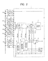
- FIG. 2 illustrates a configuration of principal parts of a battery voltage monitoring IC according to Embodiment 2.
- the battery voltage monitoring IC according to Embodiment 2 adds the cell balance function and the fault detection function of a switch for attaining a cell balance to the battery voltage monitoring IC according to Embodiment 1.
- the cell balance function means the function for maintaining the cell voltage of the plural series-coupled unit cells at an approximately equal value. A unit cell exhibiting a higher cell voltage compared with other unit cells is discharged by short-circuiting the terminals thereof, so that the unit cell is controlled to exhibit a substantially equal cell voltage as the other unit cells. What is necessary is to be balanced approximately and controlling to a strictly equal voltage is not necessary. Depending on a path which transmits current when the terminals of a unit cell is short-circuited, three kinds of modifications are possible.
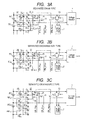
- FIGS. 3A, 3B, and 3C are explanatory diagrams illustrating modified examples of the battery voltage monitoring IC provided with cell balance function; FIG. 3A illustrates a separated drain type, FIG. 3B illustrates a separated discharge path type, and FIG. 3C illustrates a separated drain/source type. Each feature will be described later.
- the battery voltage monitoring IC illustrated in FIG. 2 is the example which adopts the separated drain type illustrated in FIG. 3A .
- terminals B 0 - B 12 for the cell balance are provided.
- the terminals B 0 - B 12 are coupled via resistors RB 0 - RB 12 to the nodes coupled in series across both poles of the unit cells BC 1 - BC 12 .
- FIG. 2 illustrates only the unit cell BC n , for simplicity.
- a switch 12 is provided for short-circuiting the terminal B n and the terminal C n-1 .
- an up-convert level shifter 5 is provided in order to generate a high-potential-side cell balance enable signal EN_H CB which controls ON and OFF of the switch 12.
- the up-convert level shifter 5 performs the level conversion of a low-potential-side cell balance enable signal EN_L CB , and generates the high-potential-side cell balance enable signal EN_H CB .
- Switches 13 and 14 are provided in parallel between a down-convert level shifter 2 and the terminal C n .
- the switch 13 is on/off controlled by a high-potential-side sense enable signal EN_H MON .
- an up-convert level shifter 4 is provided in order to generate the high-potential-side monitor enable signal EN_H MON from a low-potential-side monitor enable signal EN_L MON .
- the signal from the terminal B n is supplied to the switch 14.
- the switch 12 is provided between the signal from the terminal B n and the terminal C n-1 , and the signal from the terminal B n is pulled-up to the terminal C n via a resistor R CB .
- the switch 12 When the cell voltage of the unit cell BC n becomes higher than those of other unit cells, the switch 12 is closed to discharge the unit cell BC n .
- the path through which the discharge current flows starts from the positive electrode of the unit cell BC n , passes through a resistor RB n , the terminal B n , the switch 12, the terminal C n-1 , and a resistor Rf n-1 , and returns to the negative electrode of the unit cell BC n .
- the switch 13 is set to OFF by the high-potential-side sense enable signal EN_H MON .
- EN_H MON the high-potential-side sense enable signal
- the switch 12 When the switch 12 is closed and the switch 12 works normally, the potential difference between the terminal B n and the terminal C n-1 becomes nearly 0V. It is because the on-resistance of the switch 12 is designed to be lower enough than the resistor RB n , accordingly, the voltage drop is produced mostly in the resistor RB n . If the switch 12 is designed to have somewhat higher on-resistance and to consume electric power, there exists a possibility that the battery voltage monitoring IC 1 may be overheated.
- the switch 14 When the potential difference between the terminal B n and the terminal C n-1 becomes nearly 0V, the switch 14 is not set to ON. Since the switch 13 is also set to OFF, the down-convert level shifter 2 does not operate, and the output thereof is set to 0V.
- the switch 12 when the switch 12 is unable to be set to ON due to fault (disconnection fault), the potential of the terminal B n rises to the same potential as the terminal C n by the pull-up resistor 22. Accordingly, the switch 14 is set to ON, and the down-convert level shifter 2 operates to output the low-potential-side inter-terminal voltage corresponding to the cell voltage of the unit cell BC n .
- the switch 14 is set always to ON, even if the switch 12 is not controlled to be ON by the cell balance enable signal EN_L CB , since the switch 12 is set to ON due to fault.
- the switch 13 When the switch 13 is set to OFF by the sense enable signal EN_L MON and the switch 12 is controlled to be set to ON by the cell balance enable signal EN_L CB , if the output of the down-convert level shifter 2 becomes 0V, it is determined that the switch 12 is normal, however, if the low-potential-side inter-terminal voltage corresponding to the cell voltage of the unit cell BC n is outputted, it is determined that the switch 12 is in the disconnection fault.
- the switch 13 When the switch 13 is set to OFF by the sense enable signal EN_L MON and the switch 12 is controlled to be set to OFF by the cell balance enable signal EN_L CB , if the output of the down-convert level shifter 2 becomes 0V, it is determined that the switch 12 is in the sticking conduction fault, however, if the low-potential-side inter-terminal voltage corresponding to the cell voltage of the unit cell BC n is outputted, it is determined that the switch 12 is normal.
- the switch 13 and the switch 14 may be formed by an n-channel FET or a p-channel FET. The signal level for the on-off control described above may be adjusted suitably, according to the type of FET adopted in the switch.
- the present structure it is possible to realize, with a circuit formed on a single semiconductor substrate, the fault detection of the switch (12) which discharges a unit cell in order to realize the cell balance function, while satisfying the functional safety standards with dual-redundancy with the monitoring of a battery voltage.
- FIGS. 3A, 3B, and 3C are explanatory diagrams illustrating modified examples of the battery voltage monitoring IC provided with cell balance function;
- FIG. 3A illustrates a separated drain type
- FIG. 3B illustrates a separated discharge path type
- FIG. 3C illustrates a separated drain/source type.
- the separated drain type illustrated in FIG. 3A is adopted.
- terminals B 0 - B 12 for the cell balance are provided in addition to the terminals C 0 - C 12 .
- the terminals B 0 - B 12 are coupled via resistors RB 0 - RB 12 to the nodes coupled in series across both poles of the unit cells BC 1 - BC 12 .
- a switch 12 is provided for short-circuiting the terminal B n and the terminal C n-1 .
- the path for discharging the unit cell BC n is from the resistor RB n , via the terminal B n , the switch 12_n, and the terminal C n-1 , and to the resistor Rf n-1 .
- the path for discharging an adj oining unit cell BC n-1 is from a resistor RB n-1 , via a terminal B n-1 , a switch 12_n-1, and a terminal C n-2 , and to a resistor Rf n-2 .
- terminals B 0 - B 12 for the cell balance are provided in addition to the terminals C 0 - C 12 .
- the terminals B 0 - B 12 are coupled via resistors RB 0 - RB 12 to the nodes coupled in series across both poles of the unit cells BC 1 - BC 12 .
- a switch 15 for discharging the unit cell BC n is provided so as to short-circuit the terminal B n and the terminal B n-1 .
- the path for discharging the unit cell BC n is from the resistor RB n , via the terminal B n , the switch 15_n, and the terminal B n-1 , and to the resistor RB n-1 .
- the separated discharge path type it is not possible to discharge the adjoining unit cells concurrently. This is because, if a switch 15_n-1 for discharging the adjoining unit cell is set to ON concurrently with the switch 15_n, the discharge current flows not through the discharge path described above but towards the switch 15_n-1.
- the wiring resistance Rf n and Rf n-1 are not included in the discharge path, therefore, it is possible to measure the cell voltage of the unit cell BC n by the voltage measurement unit 7 during the discharging period for the cell balance.
- a switch 16 for discharging the unit cell BC n is provided so as to short-circuit the terminal BD n and the terminal BS n .
- the path for discharging the unit cell BC n is from the resistor RB n , via the terminal BD n , the switch 16_n, and the terminal BS n , and to a resistor RB' n .
- the wiring resistance Rf n and Rf n-1 are not included in the discharge path; therefore, it is possible to measure the cell voltage of the unit cell BC n by the voltage measurement unit 7 during the discharging period for the cell balance as well.
- the type illustrated in FIG. 3C requires more numbers of terminals, but exhibits the improved performance.
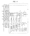
- FIG. 4 is an explanatory diagram illustrating an example in which a down-convert level shifter circuit 2 of the battery voltage monitoring IC is comprised of a high withstand voltage MOSFET.
- MOSFETs 31, 32, and 33 of which the gate electrodes are depicted with a thick outline bar are high withstand voltage MOSFETs. It is possible to realize the high withstand voltage by the well-known methods, such as by thickening a gate oxide layer or providing a drain with an offset region.
- the down-convert level shifter circuit 2 is comprised of a voltage-to-current converter circuit 8 and a current-to-voltage converter circuit 9.
- the voltage-to-current converter circuit 8 is comprised of the high withstand voltage MOSFET 31 and a resistor 23, and converts the voltage between the terminals C n and C n-1 as the cell voltage of the unit cell BC n into a conversion current of the corresponding current value.
- an inter-terminal voltage is V BH
- a threshold voltage of the high withstand voltage MOSFET 31 is Vt 31
- a value of resistance of the resistor 23 Rs 23
- the current-to-voltage converter circuit 9 is comprised of the high withstand voltage MOSFET 32 and a resistor 24, and outputs a low-potential-side inter-terminal voltage corresponding to the converted conversion current.
- a threshold voltage of the high withstand voltage MOSFET 32 is Vt 32 and a value of resistance of the resistor 24 is Rs 24
- the low-potential-side inter-terminal voltage VBL Vt 32 + IcRs 24 .
- a gate and a source of the high withstand voltage MOSFET 32 are short-circuited to form a diode; therefore, a forward voltage drop which corresponds to the threshold voltage Vt 32 is generated.
- FIG. 6 is an explanatory diagram illustrating an example in which an up-convert level shifter circuit of the battery voltage monitoring IC is comprised of a high withstand voltage MOSFET.
- FIG. 6 illustrates a circuit which outputs the high-potential-side control signal for driving a switch comprised of a p-channel MOSFET 30_8.
- the lower part of FIG. 6 illustrates a circuit which outputs the high-potential-side control signal for driving a switch comprised of an n-channel MOSFET 30_7.
- the high withstand voltage MOSFET 35 performs the on-off control of the output current of the current mirror 51 according to the value of the low-potential-side control signal.
- the high withstand voltage MOSFET 35 makes the output current of the current mirror 51 flow through the resistor 26. Accordingly, a voltage drop is generated across the resistor 26, and a high-potential-side control signal is generated, which is based on the potential of one of the terminals C 0 - C 12 as a reference potential. Since the high-potential-side control signal is lower than the terminal voltage, it is suitable for control of the switch comprised of the p-channel MOSFET 30_8.
- a gate of the high withstand voltage MOSFET 34 is supplied with the other of the low-potential-side control signals, and a drain thereof is coupled to a current mirror 52.
- the output of the current mirror 52 is coupled to a resistor 25 and a gate of the n-channel MOSFET 30_7 which configures a switch.
- This signal line corresponds to the high-potential-side control signal.
- the other side of the resistor 25 is coupled to a source of the n-channel MOSFET 30_7 which configures the switch.
- This signal line corresponds to one of the terminals C 0 - C 12 illustrated in FIG. 2 .
- the switch 12 for the cell balance function needs the enlarged area of the switch itself in order to make large current flow. Therefore, even if the number of the current mirrors 52 increases, configuring comparatively many switches of the n-channel MOSFET 30_7 can reduce the entire chip area. On the other hand, the switches 11 and 13 do not make large current flow; therefore, the area of the switch itself can be made small. Therefore, configuring comparatively many switches of the p-channel MOSFET 30_8 and suppressing the number of the current mirrors 52 to be employed can reduce the entire chip area.
- the switch comprised of the n-channel MOSFET 30_7 When the switch comprised of the n-channel MOSFET 30_7 is adopted sequentially from the comparatively low potential side, it is preferable to determine suitably the power supply voltage of the current mirror 52, the necessity of the high withstand voltage MOSFETs 36 and 37, or the number of stages, in accordance with the potential of the high-potential-side control signal to drive.
- the switch comprised of the n-channel MOSFET 30_7 is arranged at the lowest potential side, it is also preferable to couple directly the low-potential-side control signal to drive, without employing a level shifter circuit.
- a high withstand voltage MOSFET of the same kind as the MOSFET 33 illustrated in FIG. 4 is inserted in the middle of the input-output current path of a current mirror; accordingly, the withstand voltage can be distributed.
- FIG. 7 is an explanatory diagram illustrating an example in which the up-convert level shifter circuit of the battery voltage monitoring IC is comprised of a high withstand voltage bipolar transistor.
- the up-convert level shifter circuits 3, 4, and 5 convert a low-potential-side control signal (EN_L TAP , EN_L CB , EN_L MON ) into a high-potential-side control signal (EN_H TAP , EN_H CB , EN_H MON ).
- Each of the low-potential-side control signal and the high-potential-side control signal can employ the bus arrangement formed by 12 signal lines respectively corresponding to 12 unit cells.
- FIG. 7 illustrates an example in which two low-potential-side control signals are shifted to two high-potential-side control signals.
- the low-potential-side control signals are stored in a register 10. The upper part of FIG.
- FIG. 7 illustrates a circuit which outputs the high-potential-side control signal for driving a switch comprised of a p-channel MOSFET 30_8.
- the lower part of FIG. 7 illustrates a circuit which outputs the high-potential-side control signal for driving a switch comprised of an n-channel MOSFET 30_7.
- Bipolar transistors 44, 45, 46, and 47 are high withstand voltage transistors, and MOSFETs are ordinary low withstand voltage MOSFETs.
- a current mirror 51 comprised of MOSFETs 30_1, 30_2, and 30_3 is provided.
- the current mirror 51 is supplied with a reference current I ref and outputs a current at a predetermined magnification of the reference current to the bipolar transistor 45 via the MOSFET 30_2, and to the bipolar transistor 44 via the MOSFET 30_3, respectively.
- the bipolar transistor 45 performs the on-off control of the output current of the current mirror 51 according to the value of the low-potential-side control signal.
- the bipolar transistor 45 makes the output current of the current mirror 51 flow through the resistor 26. Accordingly, a voltage drop is generated across the resistor 26, and a high-potential-side control signal is generated, which is based on the potential of one of the terminals C 0 - C 12 as a reference potential. Since the high-potential-side control signal is lower than the terminal voltage, it is suitable for control of the switch comprised of the p-channel MOSFET 30_8.
- a base of bipolar transistor 44 is supplied with the other of the low-potential-side control signals, and a collector thereof is coupled to a current mirror 53.
- the output of the current mirror 53 is coupled to a resistor 25 and a gate of an n-channel MOSFET 30_7 which configures a switch.
- This signal line corresponds to the high-potential-side control signal.
- the other side of the resistor 25 is coupled to a source of the n-channel MOSFET 30_7 which configures the switch.
- This signal line corresponds to one of the terminals C 0 - C 12 illustrated in FIG. 2 .
- the bipolar transistor 44 performs the on-off control of the output current of the current mirror 51 according to the value of the low-potential-side control signal.
- the current further mirrored by the current mirror 53 flows through the resistor 25. Accordingly, a voltage drop is generated across the resistor 25, and a high-potential-side control signal is generated, which is based on the potential of one of the terminals C 0 - C 12 as a reference potential. Since the high-potential-side control signal is higher than the terminal voltage, it is suitable for control of the switch comprised of the n-channel MOSFET 30_7.
- the comparator circuit 6 is comprised of a high-voltage-side comparator circuit (CCOMP1 - CCOMP12) which compares the cell voltage shifted to the low potential side by a down-convert level shifter circuit 2, with a high-voltage-side reference voltage (V ref H), and a low-voltage-side comparator circuit (DCOMP1 - DCOMP12) which compares the cell voltage shifted to the low potential side, with a low-voltage-side reference voltage (V ref L).
- CCOMP1 - CCOMP12 high-voltage-side comparator circuit
- V ref H high-voltage-side reference voltage
- DCOMP1 - DCOMP12 low-voltage-side comparator circuit
- the battery voltage monitoring IC (semiconductor device) 1 is provided with terminals B 0 - B 12 in addition to the terminals C 0 - C 12 , and switches S CB 12 - S CB 1 for short-circuiting the terminal B n and the terminal C n-1 . It is possible to employ a cell balance circuit of other types than ones illustrated in FIGS. 3A, 3B, and 3C . By discharging selectively a unit cell whose cell voltage is higher than the other unit cells, it is possible to control the cell voltage of all the unit cells so as to be approximately equal.
- the high-potential-side control signals EN_H TAP , EN_H CB , and EN_H MON which control respectively the switches S TAP 12 - S TAP 1, the switches S CB 12 - S CB 1, and the MOSFETs M M 12 - M M 1 configuring the switch 13, are generated by level-shifting the potential of the low-potential-side control signals EN_L TAP , EN_L CB , and EN_L MON by the up-convert level shifter circuits 3, 4, and 5. It is possible to employ the circuit illustrated in Embodiments 6 or 7 for the circuit of the up-convert level shifters 3, 4, and 5.
- the low-potential-side control signals EN_L TAP , EN_L CB , and EN_L MON are stored in the register 10.
- the battery voltage monitoring IC 1 is further provided with a logic circuit 63 including the register 10, and an SPI (Serial Peripheral Interface) control circuit as a communication interface 62.
- the register 10 can be accessed from the exterior via the communication interface 62.
- the logic circuit 63 can receive an interrupt INTI from the exterior, and can issue an interrupt INTO to the exterior. For example, when abnormal conditions are detected by the fault monitoring function, such as the fault detection, not only the abnormal conditions are stored in the register 10, but the interrupt INTO is issued to notify the abnormal conditions more positively.
- FIG. 9 illustrates a configuration of principal parts of a battery voltage monitoring device 70.
- Plural unit cells which configure an assembled battery are divided into groups of series-coupled plural unit cells, and the battery voltage monitoring ICs 1_1 - 1_M are coupled to each group.
- the battery voltage monitoring device 70 is further provided with a battery system controller 60.
- the battery system controller 60 is coupled to a communication interface 62 of the battery voltage monitoring ICs 1_1 - 1_M through a communication path 61 which is formed by use of a daisy chain, for example.
- the battery voltage monitoring IC which is applied to an assembled battery comprised of unit cells (battery cells) series-coupled in multi-stage has been explained. It is effective to employ secondary cells, such as a lithium-ion battery, a nickel-hydrogen battery, and a fuel cell, as the unit cell and to apply the battery voltage monitoring IC in order to monitor the charge and discharge state of the secondary cells. It is also effective to apply the battery voltage monitoring IC as the voltage monitoring device for an assembled battery comprised of series-coupled primary cells, and for the power source in which large capacity capacitors, such as electric double layer capacitors and lithium-ion capacitors, etc. are series-coupled inmulti-stage.
Landscapes
- Engineering & Computer Science (AREA)
- Power Engineering (AREA)
- Physics & Mathematics (AREA)
- General Physics & Mathematics (AREA)
- Secondary Cells (AREA)
- Charge And Discharge Circuits For Batteries Or The Like (AREA)
- Measurement Of Current Or Voltage (AREA)
Applications Claiming Priority (1)
| Application Number | Priority Date | Filing Date | Title |
|---|---|---|---|
| JP2012185120A JP5932569B2 (ja) | 2012-08-24 | 2012-08-24 | 半導体装置及び電池電圧監視装置 |
Publications (3)
| Publication Number | Publication Date |
|---|---|
| EP2700965A2 true EP2700965A2 (fr) | 2014-02-26 |
| EP2700965A3 EP2700965A3 (fr) | 2017-05-10 |
| EP2700965B1 EP2700965B1 (fr) | 2020-10-07 |
Family
ID=48914147
Family Applications (1)
| Application Number | Title | Priority Date | Filing Date |
|---|---|---|---|
| EP13179215.2A Active EP2700965B1 (fr) | 2012-08-24 | 2013-08-05 | Dispositif semi-conducteur et dispositif de surveillance de tension de batterie |
Country Status (3)
| Country | Link |
|---|---|
| US (2) | US9735567B2 (fr) |
| EP (1) | EP2700965B1 (fr) |
| JP (1) | JP5932569B2 (fr) |
Cited By (7)
| Publication number | Priority date | Publication date | Assignee | Title |
|---|---|---|---|---|
| CN104953684A (zh) * | 2015-06-23 | 2015-09-30 | 深圳市科列技术股份有限公司 | 一种电池管理系统的动态均衡电路及其动态均衡方法 |
| DE102015202567A1 (de) * | 2015-02-12 | 2016-08-18 | Robert Bosch Gmbh | Batteriesystem mit einer Batterie und mehreren Messeinheiten zum Messen einer mittels mindestens einer Batteriezelle der Batterie bereitgestellte Spannung und Verfahren zum Messen einer mittels mindestens einer Batteriezelle einer Batterie bereitgestellte Spannung |
| US20170033570A1 (en) * | 2015-07-30 | 2017-02-02 | Lapis Semiconductor Co., Ltd. | Semiconductor device and cell voltage equalization method for battery cell |
| CN109283470A (zh) * | 2018-10-24 | 2019-01-29 | 南宁学院 | 一种动力电池组单体电压监测电路 |
| WO2020015502A1 (fr) * | 2018-07-17 | 2020-01-23 | 深圳市道通智能航空技术有限公司 | Procédé et dispositif de suivi de décharge excessive de batterie, puce, batterie, et aéronef |
| EP3757594A4 (fr) * | 2018-11-02 | 2021-06-30 | Lg Chem, Ltd. | Appareil et procédé de diagnostic de capteur de courant |
| WO2021191894A1 (fr) * | 2020-03-22 | 2021-09-30 | Irp Nexus Group Ltd | Système de gestion de batterie (bms) et application |
Families Citing this family (20)
| Publication number | Priority date | Publication date | Assignee | Title |
|---|---|---|---|---|
| JPH0487323A (ja) * | 1990-07-31 | 1992-03-19 | Mitsubishi Electric Corp | Cvd装置 |
| JP5932569B2 (ja) * | 2012-08-24 | 2016-06-08 | ルネサスエレクトロニクス株式会社 | 半導体装置及び電池電圧監視装置 |
| KR101589198B1 (ko) * | 2013-02-19 | 2016-01-28 | 주식회사 엘지화학 | 셀 밸런싱 회로의 고장 진단 장치 및 방법 |
| JP6152815B2 (ja) * | 2014-03-25 | 2017-06-28 | 株式会社豊田自動織機 | 電池監視装置 |
| EP3149499B1 (fr) * | 2014-06-02 | 2018-01-31 | Volvo Truck Corporation | Procédé et système permettant de surveiller l'état d'éléments de batterie |
| US9857431B2 (en) * | 2014-07-23 | 2018-01-02 | Gm Global Technology Operation Llc | Battery cell voltage sensing circuit diagnostics |
| CN114609426A (zh) * | 2015-09-17 | 2022-06-10 | 新唐科技日本株式会社 | 电压检测电路、异常检测装置、以及电池系统 |
| KR101846200B1 (ko) | 2016-11-09 | 2018-04-06 | 현대오트론 주식회사 | 배터리 관리 시스템의 단선 검출 장치 및 방법 |
| JP7014565B2 (ja) * | 2016-12-15 | 2022-02-01 | エイブリック株式会社 | 二次電池監視装置及び故障診断方法 |
| US10288694B2 (en) * | 2016-12-15 | 2019-05-14 | Ablic Inc. | Secondary battery monitoring device and method for diagnosing failure |
| KR102236384B1 (ko) * | 2017-10-27 | 2021-04-05 | 주식회사 엘지화학 | 배터리 밸런싱을 위한 장치 및 그것을 포함하는 배터리팩 |
| CN111279569B (zh) * | 2017-10-30 | 2022-07-19 | 新唐科技日本株式会社 | 电源保护电路 |
| CN110350262B (zh) * | 2018-04-02 | 2021-03-05 | 南京德朔实业有限公司 | 电池包及充电组合 |
| KR102500362B1 (ko) * | 2018-10-19 | 2023-02-14 | 주식회사 엘지에너지솔루션 | 배터리 관리 장치 |
| CN111337837B (zh) * | 2018-12-18 | 2022-07-05 | 华润微集成电路(无锡)有限公司 | 一种电压采样电路及电压采样方法 |
| CN113544896B (zh) * | 2019-03-06 | 2024-06-28 | 三洋电机株式会社 | 异常诊断系统和车辆用电源系统 |
| US11495976B2 (en) * | 2019-10-01 | 2022-11-08 | Samsung Sdi Co., Ltd. | Battery system and method for controlling battery system |
| EP3806226A1 (fr) * | 2019-10-09 | 2021-04-14 | NXP USA, Inc. | Mesures de tension redondant pour systèmes de gestion de batterie |
| CN113972907A (zh) * | 2020-07-24 | 2022-01-25 | 雅特力科技(重庆)有限公司 | 针对电池电压的分压器电路及具备分压器电路的电子装置 |
| JP6912744B1 (ja) * | 2020-08-28 | 2021-08-04 | ミツミ電機株式会社 | 制御システム、制御方法及び二次電池保護集積回路 |
Citations (4)
| Publication number | Priority date | Publication date | Assignee | Title |
|---|---|---|---|---|
| JP2006064639A (ja) | 2004-08-30 | 2006-03-09 | Renesas Technology Corp | 電池電圧監視装置 |
| JP2006275928A (ja) | 2005-03-30 | 2006-10-12 | Nec Electronics Corp | 電池電圧測定装置 |
| WO2007119682A1 (fr) | 2006-04-13 | 2007-10-25 | Panasonic Corporation | Bloc-batterie et procédé de détection de disjonction du bloc-batterie |
| JP2008164567A (ja) | 2007-01-05 | 2008-07-17 | Nec Electronics Corp | 電池電圧監視装置 |
Family Cites Families (11)
| Publication number | Priority date | Publication date | Assignee | Title |
|---|---|---|---|---|
| JP2001224138A (ja) * | 2000-02-07 | 2001-08-17 | Hitachi Ltd | 蓄電装置及び蓄電器の電圧検出方法 |
| JP4605952B2 (ja) * | 2001-08-29 | 2011-01-05 | 株式会社日立製作所 | 蓄電装置及びその制御方法 |
| JP4199578B2 (ja) * | 2003-04-04 | 2008-12-17 | 日本電気株式会社 | 電圧検出回路 |
| JP2006185685A (ja) * | 2004-12-27 | 2006-07-13 | Nissan Motor Co Ltd | 断線検出装置および断線検出方法 |
| JP5133926B2 (ja) * | 2009-03-26 | 2013-01-30 | 株式会社日立製作所 | 車両用電池システム |
| US8629687B2 (en) * | 2009-04-24 | 2014-01-14 | Yazaki Corporation | Disconnection detecting device |
| WO2011052594A1 (fr) * | 2009-10-27 | 2011-05-05 | ミツミ電機株式会社 | Circuit de commande de charge/décharge, circuit intégré à semi-conducteurs, procédé de commande de charge/décharge, et programme de commande de charge/décharge |
| JP5663783B2 (ja) * | 2010-02-26 | 2015-02-04 | リコー電子デバイス株式会社 | 2次電池保護回路とバッテリ装置 |
| JP5571485B2 (ja) | 2010-07-14 | 2014-08-13 | 矢崎総業株式会社 | 組電池の電圧均等化装置 |
| JP5606997B2 (ja) * | 2011-07-27 | 2014-10-15 | 株式会社東芝 | 電池セル監視回路、電池セルモジュール、電池セルモジュールを備えた自動車 |
| JP5932569B2 (ja) * | 2012-08-24 | 2016-06-08 | ルネサスエレクトロニクス株式会社 | 半導体装置及び電池電圧監視装置 |
-
2012
- 2012-08-24 JP JP2012185120A patent/JP5932569B2/ja active Active
-
2013
- 2013-08-05 EP EP13179215.2A patent/EP2700965B1/fr active Active
- 2013-08-16 US US13/968,635 patent/US9735567B2/en active Active
-
2017
- 2017-07-06 US US15/642,939 patent/US10630067B2/en active Active
Patent Citations (4)
| Publication number | Priority date | Publication date | Assignee | Title |
|---|---|---|---|---|
| JP2006064639A (ja) | 2004-08-30 | 2006-03-09 | Renesas Technology Corp | 電池電圧監視装置 |
| JP2006275928A (ja) | 2005-03-30 | 2006-10-12 | Nec Electronics Corp | 電池電圧測定装置 |
| WO2007119682A1 (fr) | 2006-04-13 | 2007-10-25 | Panasonic Corporation | Bloc-batterie et procédé de détection de disjonction du bloc-batterie |
| JP2008164567A (ja) | 2007-01-05 | 2008-07-17 | Nec Electronics Corp | 電池電圧監視装置 |
Cited By (10)
| Publication number | Priority date | Publication date | Assignee | Title |
|---|---|---|---|---|
| DE102015202567A1 (de) * | 2015-02-12 | 2016-08-18 | Robert Bosch Gmbh | Batteriesystem mit einer Batterie und mehreren Messeinheiten zum Messen einer mittels mindestens einer Batteriezelle der Batterie bereitgestellte Spannung und Verfahren zum Messen einer mittels mindestens einer Batteriezelle einer Batterie bereitgestellte Spannung |
| CN104953684A (zh) * | 2015-06-23 | 2015-09-30 | 深圳市科列技术股份有限公司 | 一种电池管理系统的动态均衡电路及其动态均衡方法 |
| US20170033570A1 (en) * | 2015-07-30 | 2017-02-02 | Lapis Semiconductor Co., Ltd. | Semiconductor device and cell voltage equalization method for battery cell |
| US10177581B2 (en) * | 2015-07-30 | 2019-01-08 | Lapis Semiconductor Co., Ltd. | Semiconductor device and cell voltage equalization method for battery cell |
| WO2020015502A1 (fr) * | 2018-07-17 | 2020-01-23 | 深圳市道通智能航空技术有限公司 | Procédé et dispositif de suivi de décharge excessive de batterie, puce, batterie, et aéronef |
| CN109283470A (zh) * | 2018-10-24 | 2019-01-29 | 南宁学院 | 一种动力电池组单体电压监测电路 |
| CN109283470B (zh) * | 2018-10-24 | 2021-03-16 | 南宁学院 | 一种动力电池组单体电压监测电路 |
| EP3757594A4 (fr) * | 2018-11-02 | 2021-06-30 | Lg Chem, Ltd. | Appareil et procédé de diagnostic de capteur de courant |
| US11353484B2 (en) | 2018-11-02 | 2022-06-07 | Lg Energy Solution, Ltd. | Current sensor diagnosing apparatus and method |
| WO2021191894A1 (fr) * | 2020-03-22 | 2021-09-30 | Irp Nexus Group Ltd | Système de gestion de batterie (bms) et application |
Also Published As
| Publication number | Publication date |
|---|---|
| EP2700965A3 (fr) | 2017-05-10 |
| EP2700965B1 (fr) | 2020-10-07 |
| JP2014044061A (ja) | 2014-03-13 |
| JP5932569B2 (ja) | 2016-06-08 |
| US10630067B2 (en) | 2020-04-21 |
| US9735567B2 (en) | 2017-08-15 |
| US20140055896A1 (en) | 2014-02-27 |
| US20170302069A1 (en) | 2017-10-19 |
Similar Documents
| Publication | Publication Date | Title |
|---|---|---|
| US10630067B2 (en) | Semiconductor device and battery voltage monitoring device | |
| JP4982274B2 (ja) | バッテリ状態監視回路及びバッテリ装置 | |
| JP5389387B2 (ja) | バッテリ状態監視回路及びバッテリ装置 | |
| US10581124B2 (en) | Battery assembly controller which monitors voltages of secondary batteries and semiconductor integrated circuit used for the battery assembly controller | |
| JP4186916B2 (ja) | 組電池管理装置 | |
| US8227944B2 (en) | Vertical bus circuits | |
| JP6137007B2 (ja) | 異常検出装置 | |
| US20120112755A1 (en) | Battery voltage monitoring circuit | |
| CN107315107B (zh) | 半导体装置、电池监控系统以及检测方法 | |
| JP7542606B2 (ja) | 管理装置、及び電源システム | |
| JP2013234851A (ja) | 電池システム、電動車両及び電池制御装置 | |
| US10038329B2 (en) | Monitor and control module and method | |
| US9217778B2 (en) | Voltage measuring device | |
| US20100268492A1 (en) | Battery cell voltage measurement device | |
| US20120038364A1 (en) | Circuit for Monitoring of Accumulator Cells Connected in Series | |
| EP4366116A9 (fr) | Puce de protection de batterie, système de batterie et procédé de protection de batterie | |
| US7893715B2 (en) | Arrangement and method for signal transmission between different voltage domains | |
| JP2024512997A (ja) | 電圧判断回路 |
Legal Events
| Date | Code | Title | Description |
|---|---|---|---|
| PUAI | Public reference made under article 153(3) epc to a published international application that has entered the european phase |
Free format text: ORIGINAL CODE: 0009012 |
|
| AK | Designated contracting states |
Kind code of ref document: A2 Designated state(s): AL AT BE BG CH CY CZ DE DK EE ES FI FR GB GR HR HU IE IS IT LI LT LU LV MC MK MT NL NO PL PT RO RS SE SI SK SM TR |
|
| AX | Request for extension of the european patent |
Extension state: BA ME |
|
| RAP1 | Party data changed (applicant data changed or rights of an application transferred) |
Owner name: RENESAS ELECTRONICS CORPORATION |
|
| RIN1 | Information on inventor provided before grant (corrected) |
Inventor name: HAYAKAWA, HIROHIKO Inventor name: KIMURA, JUNKO Inventor name: MURAMOTO, YOSHITAKA |
|
| PUAL | Search report despatched |
Free format text: ORIGINAL CODE: 0009013 |
|
| AK | Designated contracting states |
Kind code of ref document: A3 Designated state(s): AL AT BE BG CH CY CZ DE DK EE ES FI FR GB GR HR HU IE IS IT LI LT LU LV MC MK MT NL NO PL PT RO RS SE SI SK SM TR |
|
| AX | Request for extension of the european patent |
Extension state: BA ME |
|
| RIC1 | Information provided on ipc code assigned before grant |
Ipc: G01R 31/36 20060101AFI20170406BHEP Ipc: H02J 7/00 20060101ALI20170406BHEP Ipc: G01R 19/165 20060101ALI20170406BHEP |
|
| STAA | Information on the status of an ep patent application or granted ep patent |
Free format text: STATUS: REQUEST FOR EXAMINATION WAS MADE |
|
| 17P | Request for examination filed |
Effective date: 20171109 |
|
| RBV | Designated contracting states (corrected) |
Designated state(s): AL AT BE BG CH CY CZ DE DK EE ES FI FR GB GR HR HU IE IS IT LI LT LU LV MC MK MT NL NO PL PT RO RS SE SI SK SM TR |
|
| GRAP | Despatch of communication of intention to grant a patent |
Free format text: ORIGINAL CODE: EPIDOSNIGR1 |
|
| STAA | Information on the status of an ep patent application or granted ep patent |
Free format text: STATUS: GRANT OF PATENT IS INTENDED |
|
| INTG | Intention to grant announced |
Effective date: 20200504 |
|
| GRAS | Grant fee paid |
Free format text: ORIGINAL CODE: EPIDOSNIGR3 |
|
| GRAA | (expected) grant |
Free format text: ORIGINAL CODE: 0009210 |
|
| STAA | Information on the status of an ep patent application or granted ep patent |
Free format text: STATUS: THE PATENT HAS BEEN GRANTED |
|
| AK | Designated contracting states |
Kind code of ref document: B1 Designated state(s): AL AT BE BG CH CY CZ DE DK EE ES FI FR GB GR HR HU IE IS IT LI LT LU LV MC MK MT NL NO PL PT RO RS SE SI SK SM TR |
|
| REG | Reference to a national code |
Ref country code: GB Ref legal event code: FG4D |
|
| REG | Reference to a national code |
Ref country code: CH Ref legal event code: EP Ref country code: AT Ref legal event code: REF Ref document number: 1321736 Country of ref document: AT Kind code of ref document: T Effective date: 20201015 |
|
| REG | Reference to a national code |
Ref country code: IE Ref legal event code: FG4D |
|
| REG | Reference to a national code |
Ref country code: DE Ref legal event code: R096 Ref document number: 602013073053 Country of ref document: DE |
|
| REG | Reference to a national code |
Ref country code: NL Ref legal event code: MP Effective date: 20201007 |
|
| REG | Reference to a national code |
Ref country code: AT Ref legal event code: MK05 Ref document number: 1321736 Country of ref document: AT Kind code of ref document: T Effective date: 20201007 |
|
| PG25 | Lapsed in a contracting state [announced via postgrant information from national office to epo] |
Ref country code: FI Free format text: LAPSE BECAUSE OF FAILURE TO SUBMIT A TRANSLATION OF THE DESCRIPTION OR TO PAY THE FEE WITHIN THE PRESCRIBED TIME-LIMIT Effective date: 20201007 Ref country code: RS Free format text: LAPSE BECAUSE OF FAILURE TO SUBMIT A TRANSLATION OF THE DESCRIPTION OR TO PAY THE FEE WITHIN THE PRESCRIBED TIME-LIMIT Effective date: 20201007 Ref country code: NL Free format text: LAPSE BECAUSE OF FAILURE TO SUBMIT A TRANSLATION OF THE DESCRIPTION OR TO PAY THE FEE WITHIN THE PRESCRIBED TIME-LIMIT Effective date: 20201007 Ref country code: PT Free format text: LAPSE BECAUSE OF FAILURE TO SUBMIT A TRANSLATION OF THE DESCRIPTION OR TO PAY THE FEE WITHIN THE PRESCRIBED TIME-LIMIT Effective date: 20210208 Ref country code: NO Free format text: LAPSE BECAUSE OF FAILURE TO SUBMIT A TRANSLATION OF THE DESCRIPTION OR TO PAY THE FEE WITHIN THE PRESCRIBED TIME-LIMIT Effective date: 20210107 Ref country code: GR Free format text: LAPSE BECAUSE OF FAILURE TO SUBMIT A TRANSLATION OF THE DESCRIPTION OR TO PAY THE FEE WITHIN THE PRESCRIBED TIME-LIMIT Effective date: 20210108 |
|
| REG | Reference to a national code |
Ref country code: LT Ref legal event code: MG4D |
|
| PG25 | Lapsed in a contracting state [announced via postgrant information from national office to epo] |
Ref country code: BG Free format text: LAPSE BECAUSE OF FAILURE TO SUBMIT A TRANSLATION OF THE DESCRIPTION OR TO PAY THE FEE WITHIN THE PRESCRIBED TIME-LIMIT Effective date: 20210107 Ref country code: ES Free format text: LAPSE BECAUSE OF FAILURE TO SUBMIT A TRANSLATION OF THE DESCRIPTION OR TO PAY THE FEE WITHIN THE PRESCRIBED TIME-LIMIT Effective date: 20201007 Ref country code: AT Free format text: LAPSE BECAUSE OF FAILURE TO SUBMIT A TRANSLATION OF THE DESCRIPTION OR TO PAY THE FEE WITHIN THE PRESCRIBED TIME-LIMIT Effective date: 20201007 Ref country code: SE Free format text: LAPSE BECAUSE OF FAILURE TO SUBMIT A TRANSLATION OF THE DESCRIPTION OR TO PAY THE FEE WITHIN THE PRESCRIBED TIME-LIMIT Effective date: 20201007 Ref country code: PL Free format text: LAPSE BECAUSE OF FAILURE TO SUBMIT A TRANSLATION OF THE DESCRIPTION OR TO PAY THE FEE WITHIN THE PRESCRIBED TIME-LIMIT Effective date: 20201007 Ref country code: IS Free format text: LAPSE BECAUSE OF FAILURE TO SUBMIT A TRANSLATION OF THE DESCRIPTION OR TO PAY THE FEE WITHIN THE PRESCRIBED TIME-LIMIT Effective date: 20210207 Ref country code: LV Free format text: LAPSE BECAUSE OF FAILURE TO SUBMIT A TRANSLATION OF THE DESCRIPTION OR TO PAY THE FEE WITHIN THE PRESCRIBED TIME-LIMIT Effective date: 20201007 |
|
| PG25 | Lapsed in a contracting state [announced via postgrant information from national office to epo] |
Ref country code: HR Free format text: LAPSE BECAUSE OF FAILURE TO SUBMIT A TRANSLATION OF THE DESCRIPTION OR TO PAY THE FEE WITHIN THE PRESCRIBED TIME-LIMIT Effective date: 20201007 |
|
| REG | Reference to a national code |
Ref country code: DE Ref legal event code: R097 Ref document number: 602013073053 Country of ref document: DE |
|
| PG25 | Lapsed in a contracting state [announced via postgrant information from national office to epo] |
Ref country code: SM Free format text: LAPSE BECAUSE OF FAILURE TO SUBMIT A TRANSLATION OF THE DESCRIPTION OR TO PAY THE FEE WITHIN THE PRESCRIBED TIME-LIMIT Effective date: 20201007 Ref country code: EE Free format text: LAPSE BECAUSE OF FAILURE TO SUBMIT A TRANSLATION OF THE DESCRIPTION OR TO PAY THE FEE WITHIN THE PRESCRIBED TIME-LIMIT Effective date: 20201007 Ref country code: CZ Free format text: LAPSE BECAUSE OF FAILURE TO SUBMIT A TRANSLATION OF THE DESCRIPTION OR TO PAY THE FEE WITHIN THE PRESCRIBED TIME-LIMIT Effective date: 20201007 Ref country code: LT Free format text: LAPSE BECAUSE OF FAILURE TO SUBMIT A TRANSLATION OF THE DESCRIPTION OR TO PAY THE FEE WITHIN THE PRESCRIBED TIME-LIMIT Effective date: 20201007 Ref country code: SK Free format text: LAPSE BECAUSE OF FAILURE TO SUBMIT A TRANSLATION OF THE DESCRIPTION OR TO PAY THE FEE WITHIN THE PRESCRIBED TIME-LIMIT Effective date: 20201007 Ref country code: RO Free format text: LAPSE BECAUSE OF FAILURE TO SUBMIT A TRANSLATION OF THE DESCRIPTION OR TO PAY THE FEE WITHIN THE PRESCRIBED TIME-LIMIT Effective date: 20201007 |
|
| PLBE | No opposition filed within time limit |
Free format text: ORIGINAL CODE: 0009261 |
|
| STAA | Information on the status of an ep patent application or granted ep patent |
Free format text: STATUS: NO OPPOSITION FILED WITHIN TIME LIMIT |
|
| PG25 | Lapsed in a contracting state [announced via postgrant information from national office to epo] |
Ref country code: DK Free format text: LAPSE BECAUSE OF FAILURE TO SUBMIT A TRANSLATION OF THE DESCRIPTION OR TO PAY THE FEE WITHIN THE PRESCRIBED TIME-LIMIT Effective date: 20201007 |
|
| 26N | No opposition filed |
Effective date: 20210708 |
|
| PG25 | Lapsed in a contracting state [announced via postgrant information from national office to epo] |
Ref country code: AL Free format text: LAPSE BECAUSE OF FAILURE TO SUBMIT A TRANSLATION OF THE DESCRIPTION OR TO PAY THE FEE WITHIN THE PRESCRIBED TIME-LIMIT Effective date: 20201007 Ref country code: IT Free format text: LAPSE BECAUSE OF FAILURE TO SUBMIT A TRANSLATION OF THE DESCRIPTION OR TO PAY THE FEE WITHIN THE PRESCRIBED TIME-LIMIT Effective date: 20201007 |
|
| PG25 | Lapsed in a contracting state [announced via postgrant information from national office to epo] |
Ref country code: SI Free format text: LAPSE BECAUSE OF FAILURE TO SUBMIT A TRANSLATION OF THE DESCRIPTION OR TO PAY THE FEE WITHIN THE PRESCRIBED TIME-LIMIT Effective date: 20201007 |
|
| REG | Reference to a national code |
Ref country code: CH Ref legal event code: PL |
|
| PG25 | Lapsed in a contracting state [announced via postgrant information from national office to epo] |
Ref country code: MC Free format text: LAPSE BECAUSE OF FAILURE TO SUBMIT A TRANSLATION OF THE DESCRIPTION OR TO PAY THE FEE WITHIN THE PRESCRIBED TIME-LIMIT Effective date: 20201007 |
|
| REG | Reference to a national code |
Ref country code: BE Ref legal event code: MM Effective date: 20210831 |
|
| GBPC | Gb: european patent ceased through non-payment of renewal fee |
Effective date: 20210805 |
|
| PG25 | Lapsed in a contracting state [announced via postgrant information from national office to epo] |
Ref country code: LI Free format text: LAPSE BECAUSE OF NON-PAYMENT OF DUE FEES Effective date: 20210831 Ref country code: CH Free format text: LAPSE BECAUSE OF NON-PAYMENT OF DUE FEES Effective date: 20210831 |
|
| PG25 | Lapsed in a contracting state [announced via postgrant information from national office to epo] |
Ref country code: IS Free format text: LAPSE BECAUSE OF FAILURE TO SUBMIT A TRANSLATION OF THE DESCRIPTION OR TO PAY THE FEE WITHIN THE PRESCRIBED TIME-LIMIT Effective date: 20210207 Ref country code: LU Free format text: LAPSE BECAUSE OF NON-PAYMENT OF DUE FEES Effective date: 20210805 |
|
| PG25 | Lapsed in a contracting state [announced via postgrant information from national office to epo] |
Ref country code: IE Free format text: LAPSE BECAUSE OF NON-PAYMENT OF DUE FEES Effective date: 20210805 Ref country code: GB Free format text: LAPSE BECAUSE OF NON-PAYMENT OF DUE FEES Effective date: 20210805 Ref country code: FR Free format text: LAPSE BECAUSE OF NON-PAYMENT OF DUE FEES Effective date: 20210831 Ref country code: BE Free format text: LAPSE BECAUSE OF NON-PAYMENT OF DUE FEES Effective date: 20210831 |
|
| PG25 | Lapsed in a contracting state [announced via postgrant information from national office to epo] |
Ref country code: HU Free format text: LAPSE BECAUSE OF FAILURE TO SUBMIT A TRANSLATION OF THE DESCRIPTION OR TO PAY THE FEE WITHIN THE PRESCRIBED TIME-LIMIT; INVALID AB INITIO Effective date: 20130805 |
|
| PG25 | Lapsed in a contracting state [announced via postgrant information from national office to epo] |
Ref country code: CY Free format text: LAPSE BECAUSE OF FAILURE TO SUBMIT A TRANSLATION OF THE DESCRIPTION OR TO PAY THE FEE WITHIN THE PRESCRIBED TIME-LIMIT Effective date: 20201007 |
|
| PGFP | Annual fee paid to national office [announced via postgrant information from national office to epo] |
Ref country code: DE Payment date: 20230828 Year of fee payment: 11 |
|
| PG25 | Lapsed in a contracting state [announced via postgrant information from national office to epo] |
Ref country code: MK Free format text: LAPSE BECAUSE OF FAILURE TO SUBMIT A TRANSLATION OF THE DESCRIPTION OR TO PAY THE FEE WITHIN THE PRESCRIBED TIME-LIMIT Effective date: 20201007 |
|
| PG25 | Lapsed in a contracting state [announced via postgrant information from national office to epo] |
Ref country code: TR Free format text: LAPSE BECAUSE OF FAILURE TO SUBMIT A TRANSLATION OF THE DESCRIPTION OR TO PAY THE FEE WITHIN THE PRESCRIBED TIME-LIMIT Effective date: 20201007 |
|
| PG25 | Lapsed in a contracting state [announced via postgrant information from national office to epo] |
Ref country code: MT Free format text: LAPSE BECAUSE OF FAILURE TO SUBMIT A TRANSLATION OF THE DESCRIPTION OR TO PAY THE FEE WITHIN THE PRESCRIBED TIME-LIMIT Effective date: 20201007 |