EP2700735B1 - Sputtertarget und herstellungsverfahren dafür - Google Patents
Sputtertarget und herstellungsverfahren dafür Download PDFInfo
- Publication number
- EP2700735B1 EP2700735B1 EP12774193.2A EP12774193A EP2700735B1 EP 2700735 B1 EP2700735 B1 EP 2700735B1 EP 12774193 A EP12774193 A EP 12774193A EP 2700735 B1 EP2700735 B1 EP 2700735B1
- Authority
- EP
- European Patent Office
- Prior art keywords
- powder
- sputtering target
- alloy
- starting material
- atomized
- Prior art date
- Legal status (The legal status is an assumption and is not a legal conclusion. Google has not performed a legal analysis and makes no representation as to the accuracy of the status listed.)
- Not-in-force
Links
Images


Classifications
-
- C—CHEMISTRY; METALLURGY
- C23—COATING METALLIC MATERIAL; COATING MATERIAL WITH METALLIC MATERIAL; CHEMICAL SURFACE TREATMENT; DIFFUSION TREATMENT OF METALLIC MATERIAL; COATING BY VACUUM EVAPORATION, BY SPUTTERING, BY ION IMPLANTATION OR BY CHEMICAL VAPOUR DEPOSITION, IN GENERAL; INHIBITING CORROSION OF METALLIC MATERIAL OR INCRUSTATION IN GENERAL
- C23C—COATING METALLIC MATERIAL; COATING MATERIAL WITH METALLIC MATERIAL; SURFACE TREATMENT OF METALLIC MATERIAL BY DIFFUSION INTO THE SURFACE, BY CHEMICAL CONVERSION OR SUBSTITUTION; COATING BY VACUUM EVAPORATION, BY SPUTTERING, BY ION IMPLANTATION OR BY CHEMICAL VAPOUR DEPOSITION, IN GENERAL
- C23C14/00—Coating by vacuum evaporation, by sputtering or by ion implantation of the coating forming material
- C23C14/22—Coating by vacuum evaporation, by sputtering or by ion implantation of the coating forming material characterised by the process of coating
- C23C14/34—Sputtering
- C23C14/3407—Cathode assembly for sputtering apparatus, e.g. Target
-
- B—PERFORMING OPERATIONS; TRANSPORTING
- B22—CASTING; POWDER METALLURGY
- B22F—WORKING METALLIC POWDER; MANUFACTURE OF ARTICLES FROM METALLIC POWDER; MAKING METALLIC POWDER; APPARATUS OR DEVICES SPECIALLY ADAPTED FOR METALLIC POWDER
- B22F1/00—Metallic powder; Treatment of metallic powder, e.g. to facilitate working or to improve properties
-
- B—PERFORMING OPERATIONS; TRANSPORTING
- B22—CASTING; POWDER METALLURGY
- B22F—WORKING METALLIC POWDER; MANUFACTURE OF ARTICLES FROM METALLIC POWDER; MAKING METALLIC POWDER; APPARATUS OR DEVICES SPECIALLY ADAPTED FOR METALLIC POWDER
- B22F3/00—Manufacture of workpieces or articles from metallic powder characterised by the manner of compacting or sintering; Apparatus specially adapted therefor ; Presses and furnaces
- B22F3/12—Both compacting and sintering
- B22F3/14—Both compacting and sintering simultaneously
-
- C—CHEMISTRY; METALLURGY
- C22—METALLURGY; FERROUS OR NON-FERROUS ALLOYS; TREATMENT OF ALLOYS OR NON-FERROUS METALS
- C22C—ALLOYS
- C22C1/00—Making non-ferrous alloys
- C22C1/04—Making non-ferrous alloys by powder metallurgy
-
- C—CHEMISTRY; METALLURGY
- C22—METALLURGY; FERROUS OR NON-FERROUS ALLOYS; TREATMENT OF ALLOYS OR NON-FERROUS METALS
- C22C—ALLOYS
- C22C28/00—Alloys based on a metal not provided for in groups C22C5/00 - C22C27/00
-
- C—CHEMISTRY; METALLURGY
- C22—METALLURGY; FERROUS OR NON-FERROUS ALLOYS; TREATMENT OF ALLOYS OR NON-FERROUS METALS
- C22C—ALLOYS
- C22C9/00—Alloys based on copper
-
- C—CHEMISTRY; METALLURGY
- C23—COATING METALLIC MATERIAL; COATING MATERIAL WITH METALLIC MATERIAL; CHEMICAL SURFACE TREATMENT; DIFFUSION TREATMENT OF METALLIC MATERIAL; COATING BY VACUUM EVAPORATION, BY SPUTTERING, BY ION IMPLANTATION OR BY CHEMICAL VAPOUR DEPOSITION, IN GENERAL; INHIBITING CORROSION OF METALLIC MATERIAL OR INCRUSTATION IN GENERAL
- C23C—COATING METALLIC MATERIAL; COATING MATERIAL WITH METALLIC MATERIAL; SURFACE TREATMENT OF METALLIC MATERIAL BY DIFFUSION INTO THE SURFACE, BY CHEMICAL CONVERSION OR SUBSTITUTION; COATING BY VACUUM EVAPORATION, BY SPUTTERING, BY ION IMPLANTATION OR BY CHEMICAL VAPOUR DEPOSITION, IN GENERAL
- C23C14/00—Coating by vacuum evaporation, by sputtering or by ion implantation of the coating forming material
- C23C14/22—Coating by vacuum evaporation, by sputtering or by ion implantation of the coating forming material characterised by the process of coating
- C23C14/34—Sputtering
- C23C14/3407—Cathode assembly for sputtering apparatus, e.g. Target
- C23C14/3414—Metallurgical or chemical aspects of target preparation, e.g. casting, powder metallurgy
Definitions
- the present invention relates to a sputtering target for use in forming a compound film that mainly contains Cu and Ga and a method for producing the same.
- a Cu-Ga target has been used as a material essential for producing a solar cell in which a Cu-In-Ga-Se quaternary alloy film (so-called "CIGS film”) is used as a light absorbing layer by a so-called selenization (Se) method.
- CIGS film Cu-In-Ga-Se quaternary alloy film
- Se selenization
- the selenization method is a method in which a Cu-Ga target is subject to sputtering of about 500 nm, a film stack subject to sputtering of about 500 nm consisting of the Cu-Ga target and an In film formed thereon is subject to heat treatment in an H 2 Se gas at a temperature of 500 °C, and then Se is diffused into CuGaIn to thereby form a Cu-In-Ga-Se compound film (see Patent Document 1).
- Non-Patent Document 1 proposes the fact that Na content in a precursor film (Cu-In-Ga-Se quaternary alloy film) is typically about 0.1%.
- Patent Document 2 relates to a Cu-Ga alloy sputtering target which comprises a Cu-based alloy containing Ga, has an average crystal particle diameter of 10 ⁇ m or less, and has a porosity of 0.1% or less.
- Patent Document 3 relates to improvements in the preparation of copper-bismuth alloys, with particular reference to their use in vacuum switches.
- a Na-doped Cu-Ga target also has the same problems as described above.
- the present invention has been made in view of the aforementioned circumstances, and an object of the present invention is to provide a sputtering target which has excellent machinability and is capable of forming a compound film that mainly contains Cu and Ga and a method for producing the same.
- the present inventors have studied the method for producing a sputtering target for a compound film that mainly contains Cu and Ga. Consequently, the present inventors have found that the machinability of the sputtering target can improve with small addition of Sb.
- a sputtering target according to a first aspect of the present invention is characterized in that the sputtering target has a component composition consisting of 20 to 40 at% of Ga, 0.1 to 3 at% of Sb and optionally 0.05 to 2 at% of Na with respect to all metal elements in the sputtering target, which Na is contained as an NaF compound, an Na 2 S compound or an Na 2 Se compound, and the balance composed of Cu and unavoidable impurities.
- the sputtering target according to the first aspect of the present invention contains 0.1 to 3 at% of Sb, the sputtering target can have high machinability even if the sputtering target is produced with high density.
- the reason why the amount of Sb added is set within the above range is because, if the amount of Sb added is less than 0.1 at%, the machinability improving effect of the sputtering target cannot be obtained and whereas if the amount of Sb added exceeds 3 at%, the sputtering target is susceptible to embrittlement, resulting in the readily occurrence of cracking or chipping during cutting processing.
- a sputtering target according to a second aspect of the present invention is characterized in that the sputtering target according to the first aspect of the present invention has a structure including at least one of a Sb simple substance or a compound including Sb and Cu within crystal grains or grain boundaries of an alloy phase mainly containing a Cu-Ga alloy.
- the sputtering target according to the second aspect of the present invention has a structure including at least one of a Sb simple substance or a compound including Sb and Cu within crystal grains or grain boundaries (hereinafter, may be abbreviated as "grain boundaries or the like") of an alloy phase mainly containing a Cu-Ga alloy, free-machinability can be imparted to the sputtering target by the presence of a Sb simple substance or a compound including Sb and Cu within grain boundaries or the like, resulting in an improvement in machinability.
- a sputtering target according to a third aspect of the present invention is characterized in that Ga in the sputtering target material is contained in the form of a Cu-Ga binary alloy according to the first or the second aspect of the present invention.
- the present inventors have found that, when Sb is added, the presence of Ga simple substance in the sputtering target material affects the machinability of the sputtering target. Specifically, the present inventors have found that, if a Ga simple substance is contained in the sputtering target, cracking or chipping may easily occur in the Sb-containing Cu-Ga sputtering target during machine processing after sintering.
- the sputtering target of the present invention is characterized in that Ga in the sputtering target material is contained in the form of a Cu-Ga binary alloy. Specifically, Ga is contained in the form of a Cu-Ga solid solution or an intermetallic compound, so that a working surface suitable for sputtering can be realized without the occurrence of chipping or cracking during cutting processing after sintering.
- Ga in the sputtering target is contained in the form of a Cu-Ga alloy and partially in the form of a Ga-Sb alloy.
- a sputtering target according to a fourth aspect of the present invention is characterized in that Na is contained as an NaF compound, an Na 2 S compound, or an Na 2 Se compound and Na is contained in 0.05 to 2 at% with respect to all metal elements in the sputtering target according to the first to third aspects of the present invention.
- Na is contained as an NaF compound, an Na 2 S compound, or an Na 2 Se compound and Na is contained in 0.05 to 2 at% with respect to all metal elements in the sputtering target
- a Cu-Ga film containing Na which is effective for the improvement in power generation efficiency may be formed.
- fluorine (F) and sulfur (S) entrapped in a Cu-Ga film containing Na do not particularly affect the characteristics of the light absorbing layer of a solar cell.
- the reason why the Na content is set within the above range is as follows. If the amount of Na added exceeds 2 at%, the adhesion between a Cu-Ga-Na film and an Mo electrode serving as a base layer becomes significantly weak, resulting in the occurrence of film separations during a subsequent selenization process. On the other hand, if the amount of Na added is less than 0.05 at%, the effect of improving power generation efficiency may not be obtained. It should be noted that the Na content in the Cu-Ga sputtering target is preferably in the range of 0.1 at% to 0.5 at%.
- a method for producing a sputtering target according to a fifth aspect of the present invention is a method for producing the sputtering target according to any one of the first to fourth aspects of the present invention and is characterized in that the method includes a step of producing a starting material powder that is obtained by pulverizing at least Cu, Ga and Sb as simple substances or an alloy that contains two or more of these elements; and a step of subjecting the starting material powder to hot processing in a vacuum, in an inert atmosphere or in a reducing atmosphere, wherein Ga is contained in the starting material powder in the form of a Cu-Ga alloy or in the form of a Ga-Sb alloy.
- Ga is contained in the starting material powder in the form of a Cu-Ga alloy or in the form of a Ga-Sb alloy, Ga in a sintered body structure can surely be alloyed as compared with a case where only metal Ga is contained in the starting material powder, resulting in an improvement in cutting processability of a sintered body consisting of Cu, Ga, and Sb.
- a method for producing a sputtering target according to a sixth aspect of the present invention is a method for producing the sputtering target according to the fourth aspect of the present invention and is characterized in that the method includes a step of producing a starting material powder that is obtained by preparing at least Cu, Ga and Sb as simple substances or an alloy that contains two or more of these elements as metal powder and mixing the metal powder with NaF powder, Na 2 S powder, or Na 2 Se powder; and a step of subjecting the starting material powder to hot processing in a vacuum, in an inert atmosphere or in a reducing atmosphere, wherein Ga is contained in the starting material powder in the form of a Cu-Ga alloy or in the form of a Ga-Sb alloy.
- Ga is contained in the starting material powder in the form of a Cu-Ga alloy or in the form of a Ga-Sb alloy, Ga in a sintered body structure can surely be alloyed as compared with a case where only metal Ga is contained in the starting material powder, resulting in an improvement in cutting processability of a sintered body consisting of Cu, Ga, and Sb.
- the sputtering target of the present invention contains 0.1 to 3 at% of Sb, and thus, the sputtering target can have high machinability even if the sputtering target is produced with high density.
- the sputtering target of the present invention it becomes easy to subject the sputtering target to surface processing by cutting, so that a sputtering target processing speed is fast and it also becomes easy to process the sputtering target to a complex shape.
- an Sb-containing Cu-Ga film can be formed by using the sputtering target of the present invention by the sputtering method.
- the sputtering target of the present embodiment has a component composition containing 20 to 40 at% of Ga, 0.1 to 3 at% of Sb, and the balance composed of Cu and unavoidable impurities with respect to all metal elements in the sputtering target.
- the sputtering target of the present embodiment has a structure including a Sb simple substance or a compound including Sb and Cu within crystal grains or grain boundaries of an alloy phase mainly containing a Cu-Ga alloy. Furthermore, it is preferable that, in the Sb simple substance or the compound including Sb and Cu, the number of particles having a grain diameter (inscribed circle-equivalent diameter) of 0.5 ⁇ m or greater in the area of 200 ⁇ m ⁇ 150 ⁇ m is three or greater.
- a Sb simple substance or a compound including Sb and Cu and its grain diameter dispersed within crystal grains or grain boundaries of an alloy phase mainly containing a Cu-Ga alloy can be measured by Cu, Ga, and Sb element mapping images using, for example, an electron-probe micro analyzer (EPMA).
- EPMA electron-probe micro analyzer
- Ga in the sputtering target material is contained in the form of a Cu-Ga binary alloy.
- Ga is not present in the sputtering target material as a simple substance, resulting in an improvement in machinability of the sputtering target.
- the presence/absence of a Ga simple substance and the presence/absence of a Cu-Ga alloy can be determined by, for example, X-ray diffraction (XRD) measurement of the sputtering target. Specifically, after polishing of the surfaces of these sputtering targets (Ra: 5 ⁇ m or less), XRD measurement is performed, so that the presence of a Ga simple substance can be determined by peaks at around ⁇ of 15.24° (orientation: 111), 22.77° (113), and 23.27° (202) belonging to the Ga simple substance.
- XRD X-ray diffraction
- the presence/absence of a Cu-Ga alloy can be determined by a standard diffraction curve card using XRD measurement by the same method as in the above-described method.
- a method for forming a Ga alloy in the sputtering target material include a method for adding Ga which is the starting material for the sputtering target to a starting material powder as a Cu-Ga alloy or a Cu-Ga intermetallic compound or as a Ga-Sb alloy or a Ga-Sb intermetallic compound, a method for forming an alloy by melting the starting materials Cu, Ga, and Sb together, and the like.
- Na may be contained as an NaF compound, an Na 2 S compound, or an Na 2 Se compound and Na may be contained in 0.05 to 2 at% with respect to all metal elements in the sputtering target.
- composition evaluation of the metal elements quantitative analysis is carried out using an ICP method (high frequency induction coupled plasma method) by pulverizing the sputtering target.
- ICP method high frequency induction coupled plasma method
- the method for producing the sputtering target of the present embodiment includes a step of producing a starting material powder that is obtained by pulverizing at least Cu, Ga and Sb as simple substances or an alloy that contains two or more of these elements; a step of subjecting the starting material powder to hot processing such as sintering by hot pressing (HP) or hot isostatic pressing (HIP) in a vacuum, in an inert gas atmosphere or in a reducing atmosphere or a step of subjecting the produced starting material powder to hot processing such as sintering in an unpressurized state such as in a vacuum, in an inert gas atmosphere at a pressure of from 0.01 kgf/cm 2 to 10 kgf/cm 2 , or in a reducing atmosphere after pressure molding of the produced starting material powder.
- hot processing such as sintering by hot pressing (HP) or hot isostatic pressing (HIP) in a vacuum, in an inert gas atmosphere or in a reducing atmosphere
- sintering using the hot pressing method is performed at a hot pressing temperature (retention temperature during hot pressing) in the range of from 500 °C to 650 °C.
- a hot pressing temperature retention temperature during hot pressing
- the reason why a hot pressing temperature is set within the above range is as follows. If the hot pressing temperature is less than 500 °C, the density of the sintered body becomes low, and thus, chipping may easily occur on the sintered body during cutting processing. On the other hand, if the hot pressing temperature exceeds 650 °C, Sb is eluted during hot pressing, resulting in a cause of composition deviance in the sintered body.
- the melting point of a metal Sb is around a temperature of 630 °C
- the amount of Sb added in this application does not cause the elution of Sb during hot pressing at a hot pressing temperature of 650 °C or less according to the results of research by the present inventors.
- HIP temperature retention temperature during HIP pressing
- a HIP temperature retention temperature during HIP pressing
- the reason why an HIP temperature is set within the above range is as follows. If the HIP temperature is less than 400 °C, the density of the sintered body becomes low, and thus, chipping may easily occur on the sintered body during cutting processing. On the other hand, if the HIP temperature exceeds 620 °C, Sb is eluted during HIP, resulting in a cause of composition deviance in the sintered body.
- sintering using a method for sintering the resulting molded object in vacuum, in an inert atmosphere, or in a reducing atmosphere after pressure molding of the starting material powder is performed at a sintering temperature (sintering temperature during sintering) in the range of from 550 °C to 650 °C.
- a sintering temperature is set within the above range. If the sintering temperature is less than 550 °C, the density of the sintered body becomes low, and thus, chipping may easily occur on the sintered body during cutting processing.
- the sintering temperature exceeds 650 °C, Sb is eluted during hot pressing, resulting in a cause of composition deviance in the sintered body.
- the melting point of a metal Sb is around a temperature of 630 °C, the amount of Sb added in this application does not cause the elution of Sb during sintering using the method at a sintering temperature of 650 °C or less according to the results of research by the present inventors.
- a starting material powder for use in hot processing is produced by any one of the following methods (a) to (d).
- the starting material powder produced by any one of the methods (a) to (d) is subject to hot processing by a method such as hot pressing, HIP (hot isostatic pressing), or sintering a molded object after pressure molding of the starting material powder.
- a method such as hot pressing, HIP (hot isostatic pressing), or sintering a molded object after pressure molding of the starting material powder.
- hot processing is carried out in a vacuum, in an inert gas atmosphere, or in a reducing gas atmosphere.
- the pressure applied during hot pressing or HIP may greatly affect the density of the sputtering target sintered body, and thus, the pressure to be applied during hot pressing is preferably in the range of from 100 kgf/cm 2 to 500 kgf/cm 2 .
- the pressure to be applied during HIP is preferably in the range of from 500 kgf/cm 2 to 1500 kgf/cm 2 . Also, pressurization may be performed prior to the start of the elevation of temperature for sintering or may be applied after a certain temperature is reached.
- the Sb-containing Cu-Ga sintered body is processed into a specified shape of a sputtering target using cutting processing.
- the processed sputtering target is bonded to a backing plate consisting of Cu or Cu alloy using In as a solder, and the resulting target is provided to sputtering.
- the entire sputtering target is preferably stored in a vacuum pack or a pack purged with inert gas.
- the thus produced sputtering target of the present embodiment is subject to sputtering in Ar gas by a direct-current (DC) magnetron sputtering method.
- a direct-current (DC) magnetron sputtering method for the direct-current sputtering, a pulse superimposing power supply for applying a pulse voltage or a non-pulse DC power supply may also be employed.
- the sputtering target of the present embodiment contains 0.1 to 3 at% of Sb, and thus, the sputtering target can have high machinability even if the sputtering target is produced with high density.
- the sputtering target since the sputtering target has a structure including a Sb simple substance or a compound including Sb and Cu within crystal grains or grain boundaries of an alloy phase mainly containing a Cu-Ga alloy, the bonding strength between crystal grains becomes low by the presence of a Sb simple substance or a compound including Sb and Cu within grain boundaries or the like, resulting in an improvement in machinability.
- Ga in the sputtering target material is contained in the form of a Cu-Ga binary alloy. Specifically, Ga is contained in the form of a Cu-Ga solid solution or an intermetallic compound, so that a working surface suitable for sputtering can be realized without the occurrence of chipping or cracking during cutting processing after sintering. Also, Ga in the sputtering target is contained in the form of a Cu-Ga alloy and partially in the form of a Ga-Sb alloy.
- a Cu-Ga film containing Na which is effective for the improvement in power generation efficiency may be formed by the sputtering method.
- fluorine (F) and sulfur (S) entrapped in a Cu-Ga film containing Na do not particularly affect the characteristics of the light absorbing layer of a solar cell.
- Ga is contained in the starting material powder in the form of a Cu-Ga alloy or in the form of a Ga-Sb alloy in the method for producing the sputtering target of the present embodiment, cutting processability of the sputtering target improves as compared with a case where only metal Ga is contained in the starting material powder.
- the sputtering target of the present invention and a method for producing the same will be specifically described with reference to the evaluation result of the actually produced sputtering target by way of Examples, based on the aforementioned embodiment.
- the total amount of Cu, Sb, and Ga metals was loaded into an atomizing device and was heated to 1150 °C. After confirming the fact that all metals became molten, the resulting molten metal was atomized by the atomizing device to thereby produce Cu-Ga-Sb atomized powder so as to obtain the composition in Table 1.
- Example 7 As the starting material powder in Example 7, the total amount of Sb and Ga and a half the amount of Cu were loaded into an atomizing device and were heated to 1150 °C. After confirming the fact that all metals became molten, the resulting molten metal was atomized by the atomizing device to thereby produce Cu-Ga-Sb atomized powder so as to obtain the composition in Table 1.
- the starting material powder in Example 8 the total amount of Cu, Sb, and Ga was loaded into a vacuum melting furnace and was heated to 1150 °C. After confirming the fact that all metals became molten, the resulting metal molten was poured into a water-cooled casting mold to thereby produce an ingot consisting of Cu, Ga, and Sb so as to obtain the composition in Table 1. Next, the obtained Cu-Ga-Sb ingot was pulverized into a powder having an average grain diameter of 5 ⁇ m or less to thereby produce a powder mixture of Cu, Ga, and Sb having a predetermined composition.
- Example 9 As the starting material powder in Example 9, Cu, Ga, and Sb were firstly loaded into an atomizing device and were heated to 1150 °C. After confirming the fact that all metals became molten, the resulting molten metal was atomized by the atomizing device to thereby produce Cu 57 Ga 40 Sb 3 (at%) atomized powder so as to obtain the composition of Cu 57 Ga 40 Sb 3 (at%). Next, Cu, Ga, and Sb were loaded into an atomizing device and were heated to 1150 °C.
- the resulting molten metal was atomized by the atomizing device to thereby produce Cu 67 Ga 30 Sb 3 (at%) atomized powder so as to obtain the composition of Cu 67 Ga 30 Sb 3 (at%). Furthermore, the obtained two compositions were mixed by dry ball milling for four hours to thereby produce a powder mixture of Cu, Ga, and Sb so as to obtain a predetermined composition in Table 1.
- the total amount of Cu and Ga metals was firstly loaded into an atomizing device and was heated to 1150 °C. After confirming the fact that all metals became molten, the resulting molten metal was atomized by the atomizing device to thereby produce Cu-Ga atomized powder. Next, the pulverized Sb powder having an average grain diameter of 2 ⁇ m or less was applied on the obtained Cu-Ga atomized powder and the resulting mixture was mixed by dry ball milling for eight hours to thereby produce a powder mixture of Cu, Ga, and Sb in Table 1 so as to obtain the composition of Cu 74 Ga 25.5 Sb 0.5 (at%).
- Example 13 As the starting material powder in Example 13, the total amount of Cu and Ga metals was loaded into an atomizing device and was heated to 1150 °C. After confirming the fact that all metals became molten, the resulting molten metal was atomized by the atomizing device to thereby produce Cu-Ga atomized powder. Next, the pulverized Sb powder having an average grain diameter of 2 ⁇ m or less and NaF powder having an average grain diameter of 1 ⁇ m or less were applied on the obtained Cu-Ga atomized powder and the resulting mixture was mixed by dry ball milling for eight hours to thereby produce a powder mixture in Table 1 so as to obtain the composition of CU 68.5 Ga 30 Sb 0.5 Na 0.5 F 0.5 (at%).
- Example 14 As the starting material powder in Example 14, the total amount of Cu and Ga metals was loaded into an atomizing device and was heated to 1150 °C. After confirming the fact that all metals became molten, the resulting molten metal was atomized by the atomizing device to thereby produce Cu-Ga atomized powder. Next, the pulverized Sb powder having an average grain diameter of 2 ⁇ m or less and NaF powder having an average grain diameter of 1 ⁇ m or less were applied on the obtained Cu-Ga atomized powder, and the resulting mixture was mixed by dry ball milling for eight hours to thereby produce a powder mixture in Table 1 so as to obtain the composition of Cu 78.5 Ga 20 Sb 0.5 Na 0.5 F 0.5 (at%).
- Example 15 As the starting material powder in Example 15, the total amount of Cu, Ga, and Sb metals was loaded into an atomizing device and was heated to 1150 °C. After confirming the fact that all metals became molten, the resulting molten metal was atomized by the atomizing device to thereby produce Cu-Ga-Sb atomized powder. Next, NaF powder having an average grain diameter of 1 ⁇ m or less was applied on the obtained Cu-Ga-Sb atomized powder, and the resulting mixture was mixed by dry ball milling for eight hours to thereby produce a powder mixture in Table 1 so as to obtain the composition of Cu 63.5 Ga 35 Sb 0.5 Na 0.5 F 0.5 (at%).
- Example 16 As the starting material powder in Example 16, a half the amount of Cu and the total amount of Ga and Sb metals were loaded into an atomizing device and were heated to 1150 °C. After confirming the fact that all metals became molten, the resulting molten metal was atomized by the atomizing device to thereby produce Cu-Ga-Sb atomized powder. Next, Cu powder having an average grain diameter of 2 ⁇ m or less and NaF powder having an average grain diameter of 1 ⁇ m or less were applied on the obtained Cu-Ga-Sb atomized powder, and the resulting mixture was mixed by dry ball milling for eight hours to thereby produce a powder mixture in Table 1 so as to obtain the composition of Cu 63.5 Ga 35 Sb 0.5 Na 0.5 F 0.5 (at%).
- Example 17 As the starting material powder in Example 17, the total amount of Cu, Ga, and Sb metals was loaded into an atomizing device and was heated to 1150 °C. After confirming the fact that all metals became molten, the resulting molten metal was atomized by the atomizing device to thereby produce Cu-Ga-Sb atomized powder. Next, Na 2 S powder having an average grain diameter of 1 ⁇ m or less was applied on the obtained Cu-Ga-Sb atomized powder, and the resulting mixture was mixed by dry ball milling for four hours to thereby produce a powder mixture in Table 1 so as to obtain the composition of Cu 63.75 Ga 35 Sb 0.5 Na 0.5 S 0.25 (at%).
- Example 18 As the starting material powder in Example 18, the total amount of Cu, Ga, and Sb metals was loaded into an atomizing device and was heated to 1150 °C. After confirming the fact that all metals became molten, the resulting molten metal was atomized by the atomizing device to thereby produce Cu-Ga-Sb atomized powder. Next, Na 2 Se powder having an average grain diameter of 1 ⁇ m or less was applied on the obtained Cu-Ga-Sb atomized powder, and the resulting mixture was mixed by dry ball milling for four hours to thereby produce a powder mixture in Table 1 so as to obtain the composition of Cu 63.75 Ga 35 Sb 0.5 Na 0.5 Se 0.25 (at%).
- the total amount of Cu and Ga metals was loaded into an atomizing device and was heated to 1150 °C. After confirming the fact that all metals became molten, the resulting molten metal was atomized by the atomizing device to thereby produce Cu-Ga atomized powder in Table 2 so as to obtain the composition of CU 75 Ga 25 (at%).
- Comparative Example 4 the total amount of Cu and Ga metals was loaded into a vacuum melting device and was heated to 1150 °C. After confirming the fact that all metals became molten, the resulting metal molten was poured into a graphite casting mold to thereby produce an ingot so as to obtain the composition of CU 75 Ga 25 (at%) in Table 2. The obtained ingot was further heated to 800 °C in nitrogen, was held for one hour, and then was subject to rolling in four passes in total at a reduction of 5% per pass.
- the total amount of Cu, Sb, and Ga metals was loaded into an atomizing device and was heated to 1150 °C. After confirming the fact that all metals became molten, the resulting molten metal was atomized by the atomizing device to thereby produce Cu-Ga-Sb atomized powder in Table 2 so as to obtain the composition of Cu 69.98 Ga 30 Sb 0.02 (at%).
- the total amount of Cu and Ga metals was firstly loaded into an atomizing device and was heated to 1150 °C. After confirming the fact that all metals became molten, the resulting molten metal was atomized by the atomizing device to thereby produce Cu-Ga atomized powder so as to obtain the composition of Cu 69.98 Ga 30 Sb 0.02 (at%). Next, the pulverized Sb powder having an average grain diameter of 2 ⁇ m or less was applied on the obtained Cu-Ga atomized powder, and the resulting mixture was mixed by dry ball milling for eight hours to thereby produce a powder mixture in Table 2.
- Comparative Example 7 the total amount of Cu, Ga, and Sb metals was loaded into a vacuum melting device and was heated to 1150 °C. After confirming the fact that all metals became molten, the resulting metal molten was poured into a graphite casting mold to thereby produce an ingot so as to obtain the composition of Cu 69.98 Ga 30 Sb 0.02 (at%) in Table 2. The obtained ingot was further heated to 600 °C in nitrogen, was held for one hour, and then was subject to rolling in four passes in total at a reduction of 5% per pass.
- the starting material powder in Comparative Example 8 the total amount of Cu, Sb, and Ga metals was loaded into an atomizing device and was heated to 1150 °C. After confirming the fact that all metals became molten, the resulting molten metal was atomized by the atomizing device to thereby produce Cu-Ga-Sb atomized powder in Table 2 so as to obtain the composition of Cu 60 Ga 35 Sb 5 (at%).
- the starting material powder in Comparative Example 9 the total amount of Cu, Ga, and Sb metals was loaded into an atomizing device and was heated to 1150 °C. After confirming the fact that all metals became molten, the resulting molten metal was atomized by the atomizing device to thereby produce Cu-Ga-Sb atomized powder. Next, NaF powder having an average grain diameter of 1 ⁇ m or less was applied on the obtained Cu-Ga-Sb atomized powder, and the resulting mixture was mixed by dry ball milling for eight hours to thereby produce a powder mixture in Table 2 so as to obtain the composition of Cu 73 Ga 20 Sb 5 Na 1.0 F 1.0 (at%).
- the total amount of Cu and Sb metals was firstly loaded into an atomizing device and was heated to 1150 °C. After confirming the fact that all metals became molten, the resulting molten metal was atomized by the atomizing device to thereby produce Cu-Sb atomized powder. At the same time, a Ga ingot was pulverized at a low temperature of 20 °C or lower and then was passed through a 0.5 mm mesh sieve to thereby produce Ga powder having a diameter of 0.5 mm or less.
- the Ga powder was applied on the obtained Cu-Sb atomized powder, and the resulting mixture was mixed by dry ball milling for one hour at a temperature of 15 °C or lower to thereby produce a powder mixture in Table 2 so as to obtain the composition of CU 61.5 Ga 35 Sb 3.5 (at%).
- the total amount of Cu, Ga, and Sb metals was firstly loaded into an atomizing device and was heated to 1150 °C. After confirming the fact that all metals became molten, the resulting molten metal was atomized by the atomizing device to thereby produce Cu-Ga-Sb atomized powder. At the same time, a Ga ingot was pulverized at a low temperature of 20 °C or lower and then was passed through a 0.5 mm mesh sieve to thereby produce Ga powder having a diameter of 0.5 mm or less.
- the pulverized Sb powder having an average grain diameter of 2 ⁇ m or less and the Ga powder were applied on the obtained Cu-Ga-Sb atomized powder, and the resulting mixture was mixed by dry ball milling for one hour at a temperature of 15 °C or lower to thereby produce a powder mixture in Table 2 so as to obtain the composition of Cu 66 Ga 32 Sb 2.0 (at%).
- the starting material powder in Comparative Example 12 the total amount of Cu and Ga metals was loaded into an atomizing device and was heated to 1150 °C. After confirming the fact that all metals became molten, the resulting molten metal was atomized by the atomizing device to thereby produce Cu-Ga atomized powder. Next, Na 2 S powder having an average grain diameter of 1 ⁇ m or less was applied on the obtained Cu-Ga atomized powder, and the resulting mixture was mixed by dry ball milling for four hours to thereby produce a powder mixture in Table 2 so as to obtain the composition of Cu 63.5 Ga 35 Na l1.0 S 0.5 (at%).
- the starting material powder in Comparative Example 13 the total amount of Cu and Ga metals was loaded into an atomizing device and was heated to 1150 °C. After confirming the fact that all metals became molten, the resulting molten metal was atomized by the atomizing device to thereby produce Cu-Ga atomized powder. Next, Na 2 Se powder having an average grain diameter of 1 ⁇ m or less was applied on the obtained Cu-Ga atomized powder, and the resulting mixture was mixed by dry ball milling for four hours to thereby produce a powder mixture in Table 2 so as to obtain the composition of Cu 63 . 5 Ga 35 Na 1.0 Se 0.5 (at%).
- these produced starting material powder in Examples and Comparative Examples were used to thereby produce sputtering targets each having a diameter of 200 mm and a thickness of 6 mm by using the vacuum hot pressing method, the HIP method, the atmosphere sintering method after pressure molding (a mixed gas of 20% hydrogen and 80% nitrogen of two atmosphere was used as the atmosphere during sintering), or the casting method as shown in Table 3 and Table 4.
- the dimension and the density of each of the obtained target were calculated and the results calculated as the theoretical density ratio were described in Table 3 and Table 4.
- the presence of a Ga simple substance in the target material was identified as a Ga simple substance using the XRD chart of the sintered targets. Specifically, after polishing of the surfaces of these sintered bodies (Ra: 5 ⁇ m or less), X-ray diffraction (XRD) was performed so that the presence of a Ga simple substance was identified by peaks at around ⁇ of 15.24° (orientation: 111), 22.77° (113), and 23.27° (202) belonging to the Ga simple substance.
- XRD X-ray diffraction
- the structure observation of the sputtering targets was performed as follows.
- the fragment of the sintered sputtering target was embedded with a resin and was then subject to wet polishing so as to obtain a flat surface.
- the surface distribution (MAPPING) of Cu, Ga, and Sb elements was measured by using an EPMA (electron-probe micro analyzer: manufactured by JEOL JXA-8500F).
- the observation conditions were as follows: an accelerating voltage of 15 kV, an irradiation current of 50 nA, a scan type of single direction, a pixel (X, Y) of (240 ,180), a spot size (X, Y) of (0.2 ⁇ m, 0.2 ⁇ m), and a measurement time of 10 mS.
- mapping element distribution was measured several times in the area of 200 x 150 ⁇ m in an observation magnification of 2,000.
- the presence/absence of a structure (hereinafter referred to as "intervening Sb phase") including at least one of a Sb simple substance or a compound including Sb and Cu within crystal grains or grain boundaries of an alloy phase mainly containing a Cu-Ga alloy was confirmed by the obtained mapping image.
- the number of particles of the intervening Sb phase having an inscribed circle-equivalent diameter of 0.5 ⁇ m or greater was measured by using the Sb composition distribution diagram. The abovementioned results were described in Table 5 and Table 6.
- the method for evaluating processability and cutting effect was performed as follows. Firstly, CuGa sintered bodies or Cu-Ga-Sb sintered bodies in Examples or Comparative Examples were subject to dry processing using a MS850G lathe manufactured by MORI SEIKI CO., LTD.
- the sintered bodies had a size with a diameter of ⁇ 80 mm and a thickness of 6 mm.
- the rotational speed during processing was 140 rpm, the amount of cutting by the cutting tool was 0.3 mm, and the feed speed was 0.097 mm/rev.
- the used cutting tool (manufactured by MITSUBISHI MATERIALS CORPORATION) has a shape model number of STFER1616H16, an insert shape model number of TEGX160302L, and a material type of HTi10. Then, the surface having a thickness of 0.5 mm was cut from each sintered body to thereby evaluate the surface of the sintered body. Specifically, surface roughness measurement and confirmation of the presence/absence of chipping of the processed surface were performed at the position 20 mm apart from the central portion of the processed sintered body. Note that the surface roughness measuring device was surftest SV-3000 manufactured by Mitsutoyo and the evaluation length was 4 mm.
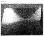
- FIG. 1 and FIG. 2 the photographs of the processed target surfaces in Example of the present invention in which the composition of Cu, Ga, and Sb was Cu 69 Ga 30 Sb 1 (at%) and in Comparative Example of the present invention in which the composition of Cu, Ga, and Sb was Cu 69 Ga 30 Sb 0.01 (at%) are shown in FIG. 1 and FIG. 2 .
- Example of the present invention in which the composition of Cu, Ga, and Sb was Cu 64 Ga 35 Sb 1 (at%) were shown in FIG. 3 . All of the original images of these EPMA images were color images but were converted into monochromatic images by gray scale. The content of Cu, Ga, and Sb tends to be high as the brightness increases.
- the obtained targets had a high density of 95% or greater in all of Examples of the present invention.
Landscapes
- Chemical & Material Sciences (AREA)
- Engineering & Computer Science (AREA)
- Mechanical Engineering (AREA)
- Materials Engineering (AREA)
- Metallurgy (AREA)
- Organic Chemistry (AREA)
- Chemical Kinetics & Catalysis (AREA)
- Manufacturing & Machinery (AREA)
- Powder Metallurgy (AREA)
- Physical Vapour Deposition (AREA)
Claims (6)
- Sputtertarget mit einer Komponentenzusammensetzung, die aus 20 bis 40 At.-% Ga, 0,1 bis 3 At.-% Sb und optional 0,05 bis 2 At.-% Na, bezogen auf alle Metallelemente in dem Sputtertarget, wobei das Na als eine NaF-Verbindung, eine Na2S-Verbindung oder eine Na2Se-Verbindung enthalten ist, und dem Rest aus Cu und unvermeidbaren Verunreinigungen besteht.
- Sputtertarget gemäß Anspruch 1, wobei das Sputtertarget eine Struktur, die mindestens einen Vertreter von einer einfachen Sb-Substanz oder einer Verbindung, beinhaltend Sb und Cu, einschließt, innerhalb der Kristallkörner oder den Korngrenzen einer Legierungsphase, die hauptsächlich eine Cu-Ga-Legierung enthält, aufweist.
- Sputtertarget gemäß Anspruch 1, wobei Ga in dem Sputtertargetmaterial in der Form einer binären Cu-Ga-Legierung enthalten ist.
- Sputtertarget gemäß Anspruch 1, wobei Na als eine NaF-Verbindung, eine Na2S-Verbindung oder eine Na2Se-Verbindung enthalten ist und Na in 0,05 bis 2 At.-%, bezogen auf alle Metallelemente, enthalten ist.
- Verfahren zur Herstellung des Sputtertargets gemäß Anspruch 1, wobei das Verfahren umfasst:einen Schritt des Herstellens eines Ausgangsmaterialpulvers, das durch Pulverisieren von mindestens Cu, Ga und Sb als einfache Substanzen oder einer Legierung, die zwei oder mehrere dieser Elemente enthält, erhalten wird; undeinen Schritt, in dem das Ausgangsmaterialpulver im Vakuum, in einer inerten Atmosphäre oder in einer reduzierenden Atmosphäre einer heißen Bearbeitung (hot processing) unterzogen wird,wobei Ga in Form einer Cu-Ga-Legierung oder in Form einer Ga-Sb-Legierung in dem Ausgangsmaterialpulver enthalten ist.
- Verfahren zur Herstellung des Sputtertargets gemäß Anspruch 4, wobei das Verfahren umfasst:einen Schritt des Herstellens eines Ausgangsmaterialpulvers, das durch Herstellen von mindestens Cu, Ga und Sb als einfache Substanzen oder eine Legierung, die zwei oder mehrere dieser Elemente enthält, als Metallpulver und Mischen des Metallpulvers mit NaF-Pulver, Na2S-Pulver oder Na2S-Pulver erhalten wird; undeinen Schritt, in dem das Ausgangsmaterialpulver im Vakuum, in einer inerten Atmosphäre oder in einer reduzierenden Atmosphäre einer heißen Bearbeitung (hot processing) unterzogen wird,wobei Ga in Form einer Cu-Ga-Legierung oder in Form einer Ga-Sb-Legierung in dem Ausgangsmaterialpulver enthalten ist.
Applications Claiming Priority (2)
| Application Number | Priority Date | Filing Date | Title |
|---|---|---|---|
| JP2011096591A JP5153911B2 (ja) | 2011-04-22 | 2011-04-22 | スパッタリングターゲット及びその製造方法 |
| PCT/JP2012/061301 WO2012144655A1 (ja) | 2011-04-22 | 2012-04-20 | スパッタリングターゲット及びその製造方法 |
Publications (3)
| Publication Number | Publication Date |
|---|---|
| EP2700735A1 EP2700735A1 (de) | 2014-02-26 |
| EP2700735A4 EP2700735A4 (de) | 2014-10-01 |
| EP2700735B1 true EP2700735B1 (de) | 2016-08-17 |
Family
ID=47041745
Family Applications (1)
| Application Number | Title | Priority Date | Filing Date |
|---|---|---|---|
| EP12774193.2A Not-in-force EP2700735B1 (de) | 2011-04-22 | 2012-04-20 | Sputtertarget und herstellungsverfahren dafür |
Country Status (7)
| Country | Link |
|---|---|
| US (1) | US9528181B2 (de) |
| EP (1) | EP2700735B1 (de) |
| JP (1) | JP5153911B2 (de) |
| KR (1) | KR101358345B1 (de) |
| CN (1) | CN103261473B (de) |
| TW (1) | TWI438296B (de) |
| WO (1) | WO2012144655A1 (de) |
Families Citing this family (5)
| Publication number | Priority date | Publication date | Assignee | Title |
|---|---|---|---|---|
| US9822430B2 (en) | 2012-02-29 | 2017-11-21 | The United States Of America As Represented By The Secretary Of The Army | High-density thermodynamically stable nanostructured copper-based bulk metallic systems, and methods of making the same |
| JP6176535B2 (ja) * | 2013-02-25 | 2017-08-09 | 三菱マテリアル株式会社 | スパッタリングターゲット及びその製造方法 |
| JP5594618B1 (ja) * | 2013-02-25 | 2014-09-24 | 三菱マテリアル株式会社 | スパッタリングターゲット及びその製造方法 |
| WO2015042622A1 (de) * | 2013-09-27 | 2015-04-02 | Plansee Se | Kupfer-gallium sputtering target |
| CN108772567A (zh) * | 2018-06-29 | 2018-11-09 | 米亚索乐装备集成(福建)有限公司 | 一种用于cig靶材打底层的合金材料、cig靶材及其制备方法 |
Family Cites Families (12)
| Publication number | Priority date | Publication date | Assignee | Title |
|---|---|---|---|---|
| GB1157652A (en) | 1966-06-15 | 1969-07-09 | Ass Elect Ind | Hardened Copper-Bismuth Base Alloys |
| JP3249408B2 (ja) | 1996-10-25 | 2002-01-21 | 昭和シェル石油株式会社 | 薄膜太陽電池の薄膜光吸収層の製造方法及び製造装置 |
| JP2002064062A (ja) * | 2000-08-17 | 2002-02-28 | Honda Motor Co Ltd | 化合物半導体の成膜方法 |
| JP4582457B2 (ja) | 2003-07-15 | 2010-11-17 | Jx日鉱日石金属株式会社 | スパッタリングターゲット及び光記録媒体 |
| US7803209B2 (en) | 2004-11-30 | 2010-09-28 | Nippon Mining & Metals Co., Ltd | Sb-Te alloy sintered compact sputtering target |
| JP2006351142A (ja) * | 2005-06-20 | 2006-12-28 | Sony Corp | 光記録媒体およびその製造方法ならびにスパッタリングターゲット |
| TWI432592B (zh) | 2007-04-27 | 2014-04-01 | Honeywell Int Inc | 具有降低預燒時間之濺鍍靶,其製造方法及其用途 |
| JP5192990B2 (ja) * | 2008-11-11 | 2013-05-08 | 光洋應用材料科技股▲分▼有限公司 | 銅−ガリウム合金スパッタリングターゲット及びそのスパッタリングターゲットの製造方法並びに関連用途 |
| US20100116341A1 (en) * | 2008-11-12 | 2010-05-13 | Solar Applied Materials Technology Corp. | Copper-gallium allay sputtering target, method for fabricating the same and related applications |
| JP5643524B2 (ja) * | 2009-04-14 | 2014-12-17 | 株式会社コベルコ科研 | Cu−Ga合金スパッタリングターゲットおよびその製造方法 |
| JP2010280944A (ja) * | 2009-06-04 | 2010-12-16 | Hitachi Cable Ltd | Cu−Ga合金、スパッタリングターゲット、Cu−Ga合金の製造方法、スパッタリングターゲットの製造方法 |
| JP4793504B2 (ja) * | 2009-11-06 | 2011-10-12 | 三菱マテリアル株式会社 | スパッタリングターゲット及びその製造方法 |
-
2011
- 2011-04-22 JP JP2011096591A patent/JP5153911B2/ja not_active Expired - Fee Related
-
2012
- 2012-04-20 CN CN201280003518.XA patent/CN103261473B/zh not_active Expired - Fee Related
- 2012-04-20 WO PCT/JP2012/061301 patent/WO2012144655A1/ja not_active Ceased
- 2012-04-20 TW TW101114153A patent/TWI438296B/zh not_active IP Right Cessation
- 2012-04-20 EP EP12774193.2A patent/EP2700735B1/de not_active Not-in-force
- 2012-04-20 US US14/111,504 patent/US9528181B2/en not_active Expired - Fee Related
- 2012-04-20 KR KR1020137011164A patent/KR101358345B1/ko not_active Expired - Fee Related
Also Published As
| Publication number | Publication date |
|---|---|
| CN103261473A (zh) | 2013-08-21 |
| US20140048414A1 (en) | 2014-02-20 |
| EP2700735A1 (de) | 2014-02-26 |
| TW201307593A (zh) | 2013-02-16 |
| EP2700735A4 (de) | 2014-10-01 |
| KR20130059458A (ko) | 2013-06-05 |
| US9528181B2 (en) | 2016-12-27 |
| JP5153911B2 (ja) | 2013-02-27 |
| JP2012229454A (ja) | 2012-11-22 |
| WO2012144655A1 (ja) | 2012-10-26 |
| CN103261473B (zh) | 2016-01-20 |
| TWI438296B (zh) | 2014-05-21 |
| KR101358345B1 (ko) | 2014-02-06 |
Similar Documents
| Publication | Publication Date | Title |
|---|---|---|
| EP2784173B1 (de) | Sputtertarget und herstellungsverfahren dafür | |
| EP2402482B1 (de) | Sputtertarget und herstellungsverfahren dafür | |
| EP2703519B1 (de) | Sputtertarget und herstellungsverfahren dafür | |
| EP2548993B1 (de) | Sputtertarget und herstellungsverfahren dafür | |
| EP2589571A1 (de) | Pulver, sinterkörper und sputtertarget, jedes mit den elementen cu, in, ga und se, sowie verfahren zur herstellung des pulvers | |
| WO2017115648A1 (ja) | スパッタリングターゲットの製造方法 | |
| EP2960355B1 (de) | Sputtertarget und herstellungsverfahren dafür | |
| EP2700735B1 (de) | Sputtertarget und herstellungsverfahren dafür | |
| EP2500447A1 (de) | Quaternäres cu-in-ga-se-legierungs-sputtertarget | |
| EP2818574A1 (de) | Sputtertarget und herstellungsverfahren dafür | |
| EP3029171A1 (de) | Cu-ga-legierungssputtertarget und verfahren zur herstellung davon | |
| EP3124647B1 (de) | Sputtertarget mit al-te-cu-zr-legierung und verfahren zur herstellung davon | |
| JP6176535B2 (ja) | スパッタリングターゲット及びその製造方法 | |
| WO2014061697A1 (ja) | Cu-Ga二元系スパッタリングターゲット及びその製造方法 | |
| JP2017014599A (ja) | スパッタリングターゲット及びその製造方法 |
Legal Events
| Date | Code | Title | Description |
|---|---|---|---|
| PUAI | Public reference made under article 153(3) epc to a published international application that has entered the european phase |
Free format text: ORIGINAL CODE: 0009012 |
|
| 17P | Request for examination filed |
Effective date: 20131021 |
|
| AK | Designated contracting states |
Kind code of ref document: A1 Designated state(s): AL AT BE BG CH CY CZ DE DK EE ES FI FR GB GR HR HU IE IS IT LI LT LU LV MC MK MT NL NO PL PT RO RS SE SI SK SM TR |
|
| DAX | Request for extension of the european patent (deleted) | ||
| A4 | Supplementary search report drawn up and despatched |
Effective date: 20140903 |
|
| RIC1 | Information provided on ipc code assigned before grant |
Ipc: C22C 28/00 20060101ALI20140828BHEP Ipc: B22F 3/14 20060101ALI20140828BHEP Ipc: C22C 1/04 20060101ALI20140828BHEP Ipc: C23C 14/34 20060101AFI20140828BHEP Ipc: B22F 1/00 20060101ALI20140828BHEP Ipc: C22C 9/00 20060101ALI20140828BHEP |
|
| RAP1 | Party data changed (applicant data changed or rights of an application transferred) |
Owner name: MITSUBISHI MATERIALS CORPORATION Owner name: SOLAR FRONTIER K.K. |
|
| GRAP | Despatch of communication of intention to grant a patent |
Free format text: ORIGINAL CODE: EPIDOSNIGR1 |
|
| RIC1 | Information provided on ipc code assigned before grant |
Ipc: B22F 1/00 20060101ALI20160311BHEP Ipc: C22C 28/00 20060101ALI20160311BHEP Ipc: C23C 14/34 20060101AFI20160311BHEP Ipc: C22C 1/04 20060101ALI20160311BHEP Ipc: B22F 3/14 20060101ALI20160311BHEP Ipc: C22C 9/00 20060101ALI20160311BHEP |
|
| INTG | Intention to grant announced |
Effective date: 20160414 |
|
| GRAS | Grant fee paid |
Free format text: ORIGINAL CODE: EPIDOSNIGR3 |
|
| GRAA | (expected) grant |
Free format text: ORIGINAL CODE: 0009210 |
|
| AK | Designated contracting states |
Kind code of ref document: B1 Designated state(s): AL AT BE BG CH CY CZ DE DK EE ES FI FR GB GR HR HU IE IS IT LI LT LU LV MC MK MT NL NO PL PT RO RS SE SI SK SM TR |
|
| REG | Reference to a national code |
Ref country code: GB Ref legal event code: FG4D |
|
| REG | Reference to a national code |
Ref country code: CH Ref legal event code: EP |
|
| REG | Reference to a national code |
Ref country code: IE Ref legal event code: FG4D |
|
| REG | Reference to a national code |
Ref country code: AT Ref legal event code: REF Ref document number: 821182 Country of ref document: AT Kind code of ref document: T Effective date: 20160915 |
|
| REG | Reference to a national code |
Ref country code: DE Ref legal event code: R096 Ref document number: 602012021945 Country of ref document: DE |
|
| REG | Reference to a national code |
Ref country code: NL Ref legal event code: MP Effective date: 20160817 |
|
| REG | Reference to a national code |
Ref country code: LT Ref legal event code: MG4D |
|
| REG | Reference to a national code |
Ref country code: AT Ref legal event code: MK05 Ref document number: 821182 Country of ref document: AT Kind code of ref document: T Effective date: 20160817 |
|
| PG25 | Lapsed in a contracting state [announced via postgrant information from national office to epo] |
Ref country code: HR Free format text: LAPSE BECAUSE OF FAILURE TO SUBMIT A TRANSLATION OF THE DESCRIPTION OR TO PAY THE FEE WITHIN THE PRESCRIBED TIME-LIMIT Effective date: 20160817 Ref country code: NL Free format text: LAPSE BECAUSE OF FAILURE TO SUBMIT A TRANSLATION OF THE DESCRIPTION OR TO PAY THE FEE WITHIN THE PRESCRIBED TIME-LIMIT Effective date: 20160817 Ref country code: RS Free format text: LAPSE BECAUSE OF FAILURE TO SUBMIT A TRANSLATION OF THE DESCRIPTION OR TO PAY THE FEE WITHIN THE PRESCRIBED TIME-LIMIT Effective date: 20160817 Ref country code: IT Free format text: LAPSE BECAUSE OF FAILURE TO SUBMIT A TRANSLATION OF THE DESCRIPTION OR TO PAY THE FEE WITHIN THE PRESCRIBED TIME-LIMIT Effective date: 20160817 Ref country code: LT Free format text: LAPSE BECAUSE OF FAILURE TO SUBMIT A TRANSLATION OF THE DESCRIPTION OR TO PAY THE FEE WITHIN THE PRESCRIBED TIME-LIMIT Effective date: 20160817 Ref country code: NO Free format text: LAPSE BECAUSE OF FAILURE TO SUBMIT A TRANSLATION OF THE DESCRIPTION OR TO PAY THE FEE WITHIN THE PRESCRIBED TIME-LIMIT Effective date: 20161117 Ref country code: FI Free format text: LAPSE BECAUSE OF FAILURE TO SUBMIT A TRANSLATION OF THE DESCRIPTION OR TO PAY THE FEE WITHIN THE PRESCRIBED TIME-LIMIT Effective date: 20160817 |
|
| PG25 | Lapsed in a contracting state [announced via postgrant information from national office to epo] |
Ref country code: PL Free format text: LAPSE BECAUSE OF FAILURE TO SUBMIT A TRANSLATION OF THE DESCRIPTION OR TO PAY THE FEE WITHIN THE PRESCRIBED TIME-LIMIT Effective date: 20160817 Ref country code: SE Free format text: LAPSE BECAUSE OF FAILURE TO SUBMIT A TRANSLATION OF THE DESCRIPTION OR TO PAY THE FEE WITHIN THE PRESCRIBED TIME-LIMIT Effective date: 20160817 Ref country code: AT Free format text: LAPSE BECAUSE OF FAILURE TO SUBMIT A TRANSLATION OF THE DESCRIPTION OR TO PAY THE FEE WITHIN THE PRESCRIBED TIME-LIMIT Effective date: 20160817 Ref country code: GR Free format text: LAPSE BECAUSE OF FAILURE TO SUBMIT A TRANSLATION OF THE DESCRIPTION OR TO PAY THE FEE WITHIN THE PRESCRIBED TIME-LIMIT Effective date: 20161118 Ref country code: LV Free format text: LAPSE BECAUSE OF FAILURE TO SUBMIT A TRANSLATION OF THE DESCRIPTION OR TO PAY THE FEE WITHIN THE PRESCRIBED TIME-LIMIT Effective date: 20160817 Ref country code: PT Free format text: LAPSE BECAUSE OF FAILURE TO SUBMIT A TRANSLATION OF THE DESCRIPTION OR TO PAY THE FEE WITHIN THE PRESCRIBED TIME-LIMIT Effective date: 20161219 Ref country code: ES Free format text: LAPSE BECAUSE OF FAILURE TO SUBMIT A TRANSLATION OF THE DESCRIPTION OR TO PAY THE FEE WITHIN THE PRESCRIBED TIME-LIMIT Effective date: 20160817 |
|
| PG25 | Lapsed in a contracting state [announced via postgrant information from national office to epo] |
Ref country code: RO Free format text: LAPSE BECAUSE OF FAILURE TO SUBMIT A TRANSLATION OF THE DESCRIPTION OR TO PAY THE FEE WITHIN THE PRESCRIBED TIME-LIMIT Effective date: 20160817 Ref country code: EE Free format text: LAPSE BECAUSE OF FAILURE TO SUBMIT A TRANSLATION OF THE DESCRIPTION OR TO PAY THE FEE WITHIN THE PRESCRIBED TIME-LIMIT Effective date: 20160817 |
|
| REG | Reference to a national code |
Ref country code: DE Ref legal event code: R097 Ref document number: 602012021945 Country of ref document: DE |
|
| PG25 | Lapsed in a contracting state [announced via postgrant information from national office to epo] |
Ref country code: SM Free format text: LAPSE BECAUSE OF FAILURE TO SUBMIT A TRANSLATION OF THE DESCRIPTION OR TO PAY THE FEE WITHIN THE PRESCRIBED TIME-LIMIT Effective date: 20160817 Ref country code: CZ Free format text: LAPSE BECAUSE OF FAILURE TO SUBMIT A TRANSLATION OF THE DESCRIPTION OR TO PAY THE FEE WITHIN THE PRESCRIBED TIME-LIMIT Effective date: 20160817 Ref country code: SK Free format text: LAPSE BECAUSE OF FAILURE TO SUBMIT A TRANSLATION OF THE DESCRIPTION OR TO PAY THE FEE WITHIN THE PRESCRIBED TIME-LIMIT Effective date: 20160817 Ref country code: DK Free format text: LAPSE BECAUSE OF FAILURE TO SUBMIT A TRANSLATION OF THE DESCRIPTION OR TO PAY THE FEE WITHIN THE PRESCRIBED TIME-LIMIT Effective date: 20160817 Ref country code: BE Free format text: LAPSE BECAUSE OF FAILURE TO SUBMIT A TRANSLATION OF THE DESCRIPTION OR TO PAY THE FEE WITHIN THE PRESCRIBED TIME-LIMIT Effective date: 20160817 Ref country code: BG Free format text: LAPSE BECAUSE OF FAILURE TO SUBMIT A TRANSLATION OF THE DESCRIPTION OR TO PAY THE FEE WITHIN THE PRESCRIBED TIME-LIMIT Effective date: 20161117 |
|
| PLBE | No opposition filed within time limit |
Free format text: ORIGINAL CODE: 0009261 |
|
| STAA | Information on the status of an ep patent application or granted ep patent |
Free format text: STATUS: NO OPPOSITION FILED WITHIN TIME LIMIT |
|
| 26N | No opposition filed |
Effective date: 20170518 |
|
| PG25 | Lapsed in a contracting state [announced via postgrant information from national office to epo] |
Ref country code: SI Free format text: LAPSE BECAUSE OF FAILURE TO SUBMIT A TRANSLATION OF THE DESCRIPTION OR TO PAY THE FEE WITHIN THE PRESCRIBED TIME-LIMIT Effective date: 20160817 |
|
| REG | Reference to a national code |
Ref country code: CH Ref legal event code: PL |
|
| GBPC | Gb: european patent ceased through non-payment of renewal fee |
Effective date: 20170420 |
|
| REG | Reference to a national code |
Ref country code: IE Ref legal event code: MM4A |
|
| REG | Reference to a national code |
Ref country code: FR Ref legal event code: ST Effective date: 20171229 |
|
| PG25 | Lapsed in a contracting state [announced via postgrant information from national office to epo] |
Ref country code: MC Free format text: LAPSE BECAUSE OF FAILURE TO SUBMIT A TRANSLATION OF THE DESCRIPTION OR TO PAY THE FEE WITHIN THE PRESCRIBED TIME-LIMIT Effective date: 20160817 Ref country code: FR Free format text: LAPSE BECAUSE OF NON-PAYMENT OF DUE FEES Effective date: 20170502 |
|
| PG25 | Lapsed in a contracting state [announced via postgrant information from national office to epo] |
Ref country code: LU Free format text: LAPSE BECAUSE OF NON-PAYMENT OF DUE FEES Effective date: 20170420 Ref country code: GB Free format text: LAPSE BECAUSE OF NON-PAYMENT OF DUE FEES Effective date: 20170420 Ref country code: LI Free format text: LAPSE BECAUSE OF NON-PAYMENT OF DUE FEES Effective date: 20170430 Ref country code: CH Free format text: LAPSE BECAUSE OF NON-PAYMENT OF DUE FEES Effective date: 20170430 |
|
| PG25 | Lapsed in a contracting state [announced via postgrant information from national office to epo] |
Ref country code: IE Free format text: LAPSE BECAUSE OF NON-PAYMENT OF DUE FEES Effective date: 20170420 |
|
| PG25 | Lapsed in a contracting state [announced via postgrant information from national office to epo] |
Ref country code: MT Free format text: LAPSE BECAUSE OF NON-PAYMENT OF DUE FEES Effective date: 20170420 |
|
| PG25 | Lapsed in a contracting state [announced via postgrant information from national office to epo] |
Ref country code: AL Free format text: LAPSE BECAUSE OF FAILURE TO SUBMIT A TRANSLATION OF THE DESCRIPTION OR TO PAY THE FEE WITHIN THE PRESCRIBED TIME-LIMIT Effective date: 20160817 |
|
| PG25 | Lapsed in a contracting state [announced via postgrant information from national office to epo] |
Ref country code: HU Free format text: LAPSE BECAUSE OF FAILURE TO SUBMIT A TRANSLATION OF THE DESCRIPTION OR TO PAY THE FEE WITHIN THE PRESCRIBED TIME-LIMIT; INVALID AB INITIO Effective date: 20120420 |
|
| PG25 | Lapsed in a contracting state [announced via postgrant information from national office to epo] |
Ref country code: CY Free format text: LAPSE BECAUSE OF NON-PAYMENT OF DUE FEES Effective date: 20160817 |
|
| PG25 | Lapsed in a contracting state [announced via postgrant information from national office to epo] |
Ref country code: MK Free format text: LAPSE BECAUSE OF FAILURE TO SUBMIT A TRANSLATION OF THE DESCRIPTION OR TO PAY THE FEE WITHIN THE PRESCRIBED TIME-LIMIT Effective date: 20160817 |
|
| PG25 | Lapsed in a contracting state [announced via postgrant information from national office to epo] |
Ref country code: TR Free format text: LAPSE BECAUSE OF FAILURE TO SUBMIT A TRANSLATION OF THE DESCRIPTION OR TO PAY THE FEE WITHIN THE PRESCRIBED TIME-LIMIT Effective date: 20160817 |
|
| PG25 | Lapsed in a contracting state [announced via postgrant information from national office to epo] |
Ref country code: IS Free format text: LAPSE BECAUSE OF FAILURE TO SUBMIT A TRANSLATION OF THE DESCRIPTION OR TO PAY THE FEE WITHIN THE PRESCRIBED TIME-LIMIT Effective date: 20161217 |
|
| PGFP | Annual fee paid to national office [announced via postgrant information from national office to epo] |
Ref country code: DE Payment date: 20220429 Year of fee payment: 11 |
|
| REG | Reference to a national code |
Ref country code: DE Ref legal event code: R119 Ref document number: 602012021945 Country of ref document: DE |
|
| PG25 | Lapsed in a contracting state [announced via postgrant information from national office to epo] |
Ref country code: DE Free format text: LAPSE BECAUSE OF NON-PAYMENT OF DUE FEES Effective date: 20231103 |