EP2693470B1 - Surface mount module with diffusion barrier and method of making the same - Google Patents
Surface mount module with diffusion barrier and method of making the same Download PDFInfo
- Publication number
- EP2693470B1 EP2693470B1 EP13177219.6A EP13177219A EP2693470B1 EP 2693470 B1 EP2693470 B1 EP 2693470B1 EP 13177219 A EP13177219 A EP 13177219A EP 2693470 B1 EP2693470 B1 EP 2693470B1
- Authority
- EP
- European Patent Office
- Prior art keywords
- layer
- diffusion barrier
- barrier layer
- level
- module
- Prior art date
- Legal status (The legal status is an assumption and is not a legal conclusion. Google has not performed a legal analysis and makes no representation as to the accuracy of the status listed.)
- Active
Links
Images


Classifications
-
- H—ELECTRICITY
- H10—SEMICONDUCTOR DEVICES; ELECTRIC SOLID-STATE DEVICES NOT OTHERWISE PROVIDED FOR
- H10W—GENERIC PACKAGES, INTERCONNECTIONS, CONNECTORS OR OTHER CONSTRUCTIONAL DETAILS OF DEVICES COVERED BY CLASS H10
- H10W74/00—Encapsulations, e.g. protective coatings
- H10W74/10—Encapsulations, e.g. protective coatings characterised by their shape or disposition
- H10W74/111—Encapsulations, e.g. protective coatings characterised by their shape or disposition the semiconductor body being completely enclosed
- H10W74/114—Encapsulations, e.g. protective coatings characterised by their shape or disposition the semiconductor body being completely enclosed by a substrate and the encapsulations
-
- H—ELECTRICITY
- H10—SEMICONDUCTOR DEVICES; ELECTRIC SOLID-STATE DEVICES NOT OTHERWISE PROVIDED FOR
- H10W—GENERIC PACKAGES, INTERCONNECTIONS, CONNECTORS OR OTHER CONSTRUCTIONAL DETAILS OF DEVICES COVERED BY CLASS H10
- H10W40/00—Arrangements for thermal protection or thermal control
- H10W40/20—Arrangements for cooling
- H10W40/25—Arrangements for cooling characterised by their materials
- H10W40/255—Arrangements for cooling characterised by their materials having a laminate or multilayered structure, e.g. direct bond copper [DBC] ceramic substrates
-
- H—ELECTRICITY
- H10—SEMICONDUCTOR DEVICES; ELECTRIC SOLID-STATE DEVICES NOT OTHERWISE PROVIDED FOR
- H10W—GENERIC PACKAGES, INTERCONNECTIONS, CONNECTORS OR OTHER CONSTRUCTIONAL DETAILS OF DEVICES COVERED BY CLASS H10
- H10W70/00—Package substrates; Interposers; Redistribution layers [RDL]
- H10W70/01—Manufacture or treatment
- H10W70/05—Manufacture or treatment of insulating or insulated package substrates, or of interposers, or of redistribution layers
- H10W70/08—Manufacture or treatment of insulating or insulated package substrates, or of interposers, or of redistribution layers by depositing layers on the chip or wafer, e.g. "chip-first" RDLs
- H10W70/09—Manufacture or treatment of insulating or insulated package substrates, or of interposers, or of redistribution layers by depositing layers on the chip or wafer, e.g. "chip-first" RDLs extending onto an encapsulation that laterally surrounds the chip or wafer, e.g. fan-out wafer level package [FOWLP] RDLs
-
- H—ELECTRICITY
- H10—SEMICONDUCTOR DEVICES; ELECTRIC SOLID-STATE DEVICES NOT OTHERWISE PROVIDED FOR
- H10W—GENERIC PACKAGES, INTERCONNECTIONS, CONNECTORS OR OTHER CONSTRUCTIONAL DETAILS OF DEVICES COVERED BY CLASS H10
- H10W70/00—Package substrates; Interposers; Redistribution layers [RDL]
- H10W70/01—Manufacture or treatment
- H10W70/05—Manufacture or treatment of insulating or insulated package substrates, or of interposers, or of redistribution layers
- H10W70/093—Connecting or disconnecting other interconnections thereto or therefrom, e.g. connecting bond wires or bumps
-
- H—ELECTRICITY
- H10—SEMICONDUCTOR DEVICES; ELECTRIC SOLID-STATE DEVICES NOT OTHERWISE PROVIDED FOR
- H10W—GENERIC PACKAGES, INTERCONNECTIONS, CONNECTORS OR OTHER CONSTRUCTIONAL DETAILS OF DEVICES COVERED BY CLASS H10
- H10W70/00—Package substrates; Interposers; Redistribution layers [RDL]
- H10W70/60—Insulating or insulated package substrates; Interposers; Redistribution layers
- H10W70/611—Insulating or insulated package substrates; Interposers; Redistribution layers for connecting multiple chips together
- H10W70/614—Insulating or insulated package substrates; Interposers; Redistribution layers for connecting multiple chips together the multiple chips being integrally enclosed
-
- H—ELECTRICITY
- H10—SEMICONDUCTOR DEVICES; ELECTRIC SOLID-STATE DEVICES NOT OTHERWISE PROVIDED FOR
- H10W—GENERIC PACKAGES, INTERCONNECTIONS, CONNECTORS OR OTHER CONSTRUCTIONAL DETAILS OF DEVICES COVERED BY CLASS H10
- H10W70/00—Package substrates; Interposers; Redistribution layers [RDL]
- H10W70/60—Insulating or insulated package substrates; Interposers; Redistribution layers
- H10W70/67—Insulating or insulated package substrates; Interposers; Redistribution layers characterised by their insulating layers or insulating parts
- H10W70/69—Insulating materials thereof
-
- H—ELECTRICITY
- H10—SEMICONDUCTOR DEVICES; ELECTRIC SOLID-STATE DEVICES NOT OTHERWISE PROVIDED FOR
- H10W—GENERIC PACKAGES, INTERCONNECTIONS, CONNECTORS OR OTHER CONSTRUCTIONAL DETAILS OF DEVICES COVERED BY CLASS H10
- H10W90/00—Package configurations
- H10W90/401—Package configurations characterised by multiple insulating or insulated package substrates, interposers or RDLs
-
- H—ELECTRICITY
- H10—SEMICONDUCTOR DEVICES; ELECTRIC SOLID-STATE DEVICES NOT OTHERWISE PROVIDED FOR
- H10W—GENERIC PACKAGES, INTERCONNECTIONS, CONNECTORS OR OTHER CONSTRUCTIONAL DETAILS OF DEVICES COVERED BY CLASS H10
- H10W90/00—Package configurations
- H10W90/701—Package configurations characterised by the relative positions of pads or connectors relative to package parts
-
- H—ELECTRICITY
- H10—SEMICONDUCTOR DEVICES; ELECTRIC SOLID-STATE DEVICES NOT OTHERWISE PROVIDED FOR
- H10W—GENERIC PACKAGES, INTERCONNECTIONS, CONNECTORS OR OTHER CONSTRUCTIONAL DETAILS OF DEVICES COVERED BY CLASS H10
- H10W42/00—Arrangements for protection of devices
-
- H—ELECTRICITY
- H10—SEMICONDUCTOR DEVICES; ELECTRIC SOLID-STATE DEVICES NOT OTHERWISE PROVIDED FOR
- H10W—GENERIC PACKAGES, INTERCONNECTIONS, CONNECTORS OR OTHER CONSTRUCTIONAL DETAILS OF DEVICES COVERED BY CLASS H10
- H10W72/00—Interconnections or connectors in packages
- H10W72/01—Manufacture or treatment
- H10W72/0198—Manufacture or treatment batch processes
-
- H—ELECTRICITY
- H10—SEMICONDUCTOR DEVICES; ELECTRIC SOLID-STATE DEVICES NOT OTHERWISE PROVIDED FOR
- H10W—GENERIC PACKAGES, INTERCONNECTIONS, CONNECTORS OR OTHER CONSTRUCTIONAL DETAILS OF DEVICES COVERED BY CLASS H10
- H10W72/00—Interconnections or connectors in packages
- H10W72/071—Connecting or disconnecting
- H10W72/073—Connecting or disconnecting of die-attach connectors
- H10W72/07331—Connecting techniques
- H10W72/07337—Connecting techniques using a polymer adhesive, e.g. an adhesive based on silicone or epoxy
- H10W72/07338—Connecting techniques using a polymer adhesive, e.g. an adhesive based on silicone or epoxy hardening the adhesive by curing, e.g. thermosetting
-
- H—ELECTRICITY
- H10—SEMICONDUCTOR DEVICES; ELECTRIC SOLID-STATE DEVICES NOT OTHERWISE PROVIDED FOR
- H10W—GENERIC PACKAGES, INTERCONNECTIONS, CONNECTORS OR OTHER CONSTRUCTIONAL DETAILS OF DEVICES COVERED BY CLASS H10
- H10W72/00—Interconnections or connectors in packages
- H10W72/20—Bump connectors, e.g. solder bumps or copper pillars; Dummy bumps; Thermal bumps
- H10W72/241—Dispositions, e.g. layouts
- H10W72/242—Dispositions, e.g. layouts relative to the surface, e.g. recessed, protruding
-
- H—ELECTRICITY
- H10—SEMICONDUCTOR DEVICES; ELECTRIC SOLID-STATE DEVICES NOT OTHERWISE PROVIDED FOR
- H10W—GENERIC PACKAGES, INTERCONNECTIONS, CONNECTORS OR OTHER CONSTRUCTIONAL DETAILS OF DEVICES COVERED BY CLASS H10
- H10W72/00—Interconnections or connectors in packages
- H10W72/20—Bump connectors, e.g. solder bumps or copper pillars; Dummy bumps; Thermal bumps
- H10W72/251—Materials
- H10W72/252—Materials comprising solid metals or solid metalloids, e.g. PbSn, Ag or Cu
-
- H—ELECTRICITY
- H10—SEMICONDUCTOR DEVICES; ELECTRIC SOLID-STATE DEVICES NOT OTHERWISE PROVIDED FOR
- H10W—GENERIC PACKAGES, INTERCONNECTIONS, CONNECTORS OR OTHER CONSTRUCTIONAL DETAILS OF DEVICES COVERED BY CLASS H10
- H10W72/00—Interconnections or connectors in packages
- H10W72/30—Die-attach connectors
- H10W72/321—Structures or relative sizes of die-attach connectors
- H10W72/325—Die-attach connectors having a filler embedded in a matrix
-
- H—ELECTRICITY
- H10—SEMICONDUCTOR DEVICES; ELECTRIC SOLID-STATE DEVICES NOT OTHERWISE PROVIDED FOR
- H10W—GENERIC PACKAGES, INTERCONNECTIONS, CONNECTORS OR OTHER CONSTRUCTIONAL DETAILS OF DEVICES COVERED BY CLASS H10
- H10W72/00—Interconnections or connectors in packages
- H10W72/30—Die-attach connectors
- H10W72/351—Materials of die-attach connectors
- H10W72/352—Materials of die-attach connectors comprising metals or metalloids, e.g. solders
-
- H—ELECTRICITY
- H10—SEMICONDUCTOR DEVICES; ELECTRIC SOLID-STATE DEVICES NOT OTHERWISE PROVIDED FOR
- H10W—GENERIC PACKAGES, INTERCONNECTIONS, CONNECTORS OR OTHER CONSTRUCTIONAL DETAILS OF DEVICES COVERED BY CLASS H10
- H10W72/00—Interconnections or connectors in packages
- H10W72/30—Die-attach connectors
- H10W72/351—Materials of die-attach connectors
- H10W72/353—Materials of die-attach connectors not comprising solid metals or solid metalloids, e.g. ceramics
- H10W72/354—Materials of die-attach connectors not comprising solid metals or solid metalloids, e.g. ceramics comprising polymers
-
- H—ELECTRICITY
- H10—SEMICONDUCTOR DEVICES; ELECTRIC SOLID-STATE DEVICES NOT OTHERWISE PROVIDED FOR
- H10W—GENERIC PACKAGES, INTERCONNECTIONS, CONNECTORS OR OTHER CONSTRUCTIONAL DETAILS OF DEVICES COVERED BY CLASS H10
- H10W72/00—Interconnections or connectors in packages
- H10W72/851—Dispositions of multiple connectors or interconnections
- H10W72/874—On different surfaces
-
- H—ELECTRICITY
- H10—SEMICONDUCTOR DEVICES; ELECTRIC SOLID-STATE DEVICES NOT OTHERWISE PROVIDED FOR
- H10W—GENERIC PACKAGES, INTERCONNECTIONS, CONNECTORS OR OTHER CONSTRUCTIONAL DETAILS OF DEVICES COVERED BY CLASS H10
- H10W74/00—Encapsulations, e.g. protective coatings
-
- H—ELECTRICITY
- H10—SEMICONDUCTOR DEVICES; ELECTRIC SOLID-STATE DEVICES NOT OTHERWISE PROVIDED FOR
- H10W—GENERIC PACKAGES, INTERCONNECTIONS, CONNECTORS OR OTHER CONSTRUCTIONAL DETAILS OF DEVICES COVERED BY CLASS H10
- H10W74/00—Encapsulations, e.g. protective coatings
- H10W74/01—Manufacture or treatment
- H10W74/014—Manufacture or treatment using batch processing
-
- H—ELECTRICITY
- H10—SEMICONDUCTOR DEVICES; ELECTRIC SOLID-STATE DEVICES NOT OTHERWISE PROVIDED FOR
- H10W—GENERIC PACKAGES, INTERCONNECTIONS, CONNECTORS OR OTHER CONSTRUCTIONAL DETAILS OF DEVICES COVERED BY CLASS H10
- H10W90/00—Package configurations
- H10W90/10—Configurations of laterally-adjacent chips
-
- H—ELECTRICITY
- H10—SEMICONDUCTOR DEVICES; ELECTRIC SOLID-STATE DEVICES NOT OTHERWISE PROVIDED FOR
- H10W—GENERIC PACKAGES, INTERCONNECTIONS, CONNECTORS OR OTHER CONSTRUCTIONAL DETAILS OF DEVICES COVERED BY CLASS H10
- H10W90/00—Package configurations
- H10W90/701—Package configurations characterised by the relative positions of pads or connectors relative to package parts
- H10W90/731—Package configurations characterised by the relative positions of pads or connectors relative to package parts of die-attach connectors
- H10W90/734—Package configurations characterised by the relative positions of pads or connectors relative to package parts of die-attach connectors between a chip and a stacked insulating package substrate, interposer or RDL
Definitions
- Embodiments of the invention relate generally to structures and methods for packaging semiconductor devices and, more particularly, to a surface-mount package structure that includes a diffusion barrier coating.
- Surface-mount technology is a method for constructing electronic circuits in which surface mount components or packages are mounted directly onto the surface of printed circuit boards (PCBs) or other similar external circuits.
- PCBs printed circuit boards
- surface-mount technology has replaced the through-hole technology construction method of fitting components with wire leads into holes in the circuit board.
- a power semiconductor device which is a semiconductor device used as a switch or rectifier in power electronic circuits, such as switched mode power supplies, for example.
- Most power semiconductor devices are only used in commutation mode (i.e., they are either on or off), and are therefore optimized for this.
- Many power semiconductor devices are used in high voltage power applications and are designed to carry a large amount of current and support a large voltage.
- high voltage power semiconductor devices are surface mounted to an external circuit by way of a power overlay (POL) packaging and interconnect system, with the POL package also providing a way to remove the heat generated by the device and protect the device from the external environment.
- POL power overlay
- a standard POL package manufacturing process typically begins with placement of one or more power semiconductor devices onto a dielectric layer by way of an adhesive.
- Metal interconnects e.g., copper interconnects
- the metal interconnects may be in the form of a low profile (e.g., less than 200 micrometers thick), planar interconnect structure that provides for formation of an input/output (I/O) system to and from the power semiconductor device(s).
- the POL sub-module is then soldered to a ceramic substrate (Alumina with DBC, A1N with AMB Cu, etc.) using soldered interconnection for electrical and thermal connectivity.
- the gaps around the semiconductor between the POL dielectric layer and the ceramic substrate are then filled using a dielectric organic material using either capillary flow (capillary underfill), no-flow underfill or injection molding (molding compounds) to form the POL package.
- POL packages are susceptible to moisture, as moisture in the environment may be absorbed by the materials in the POL package.
- the module may absorb moisture within the bulk of Kapton-adhesive layers and organic dielectric material (i.e., underfill, molding compound, etc.) and at the interfaces created by these materials within the package.
- temperatures in the range of 210-260 degrees Celsius are reached and, at these temperatures, the vapor pressure of the moisture in the POL package increases rapidly. This increase in vapor pressure can cause delamination, "pop-corning" and failure if the moisture is excessive.
- US 6306680 describes packaging of power semiconductor devices in both single chip and multiple chip packages, with enhanced electrical and thermal characteristics. US 6306680 discloses the preamble of claims 1 and 11 respectively of the present application. US 6154366 describes a chip-on-flex packaging technology which includes at least one moisture barrier layer to prevent metal corrosion and delamination of flex component layers. US 5250843 describes an improved multichip integrated circuit module including a packaging method for electronic integrated circuit chips on a substrate and having a polymer encapsulant overlying the chips. A hermetically sealed module is disclosed. US 2007/138651 describes semiconductor device packages including a direct bonded copper substrate (DBC) and processes for their manufacture.
- DBC direct bonded copper substrate
- a surface-mount package having a diffusion barrier that reduces the ingress of moisture and gases into the package, so as to provide enhanced reliability to moisture-related and gas-related failure mechanisms. It would further be desirable for such a diffusion barrier to be introduced during various stages of manufacture of the surface-mount package.
- the invention provides a surface-mount package in accordance with claim 1.
- the package includes a diffusion barrier coating configured to reduce the ingress of moisture and gases from a surrounding environment into the surface-mount structure.
- the present invention further provides a method of manufacturing a surface-mount package as defined in claim 11. Preferred embodiments are defined in the dependent claims.
- Embodiments of the present invention provide for a surface-mount package having a diffusion barrier layer included thereon, as well as a method of forming such a surface-mount package.
- the surface-mount package is manufactured such that the diffusion barrier layer reduces the ingress of moisture and gases into the package, while still providing for attaching of the surface-mount package to an external circuit.
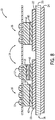
- a surface-mount packaging and interconnect structure 10 is shown according to an embodiment of the invention.
- surface-mount package structure 10 is in the form of a power overlay (POL) structure, although it is recognized that other surface-mount package structures are considered to be within the scope of the invention.
- the POL structure 10 includes one or more semiconductor device(s) 12 therein that, according to various embodiments, may be in the form of a die, diode, or other power electronic device. As shown in FIG. 1 , three semiconductor device(s) 12 are provided in POL structure 10, however, it is recognized that a greater or lesser number of semiconductor devices 12 could be included in POL structure 10.
- the semiconductor device(s) 12 are packaged within a POL sub-module 14 that forms a direct metallic connection to the power semiconductor device(s) 12, with the connection being in the form of a low profile, planar first-level interconnect structure, for example.
- a second-level input-output (I/O) connection 16 is provided on POL sub-module 14 to enable surface mounting of the POL structure 10 to an external circuit, such as a printed circuit board (PCB) (not shown).
- the second-level I/O connection 16 is formed of land grid array (LGA) solder bumps 17 that are configured to be attached/affixed to the PCB to electrically couple the POL structure 10 to the PCB, although other suitable second-level solder interconnections, such as ball grid array (BGA) solder bumps, could also be used.
- LGA solder bumps 17 provide a highly reliable interconnection structure that is resistive to failure in high stress conditions.
- POL structure 10 also includes a substrate structure 18 to which POL sub-module 14 is attached.
- the substrate structure 18 is composed of a ceramic tile (e.g., alumina) 20 with a layer of direct bond copper (DBC) 22, 24 bonded to both sides thereof by a high-temperature joining process.
- DBC direct bond copper
- different brazing and direct bond technologies may be employed based on, for example, whether tile 20 is composed of alumina or aluminum nitride and silicon nitride, etc.
- the top DBC layer 22, or "die side DBC layer,” of substrate structure 18 is then etched after firing, to pattern the layer as desired based on the number/arrangement of semiconductor devices 12.
- the bottom DBC layer 24, or "non-die side DBC layer,” on the backside of the substrate structure 18 is left fully or partially exposed to provide efficient heat transfer out from the POL structure 10.
- DBC layers While referred to above and here below as “DBC layers,” it is recognized that aluminum can be used instead of copper as the metal layers, and thus such an embodiment is considered within the scope of the invention.
- use of the term “DBC layers” here below is meant to encompass a substrate structure 18 that includes sheets of any suitable metallic material 22, 24 (such as copper or aluminum) bonded to both sides of a ceramic tile (e.g., alumina) 20. As shown in FIG.
- a dielectric material 26 is also provided on POL structure 10 to fill in gaps in the POL structure 10, so as to provide additional structural integrity to POL structure 10.
- the dielectric material 26 is generally referred to hereafter as an "underfill material," and in a preferred embodiment is an organic dielectric material that is moisture sensitive and that flows as a liquid prior to curing.
- underfill material an organic dielectric material that is moisture sensitive and that flows as a liquid prior to curing.
- the dielectric material 26 could be formed of any of a number of suitable materials, including underfills, silicones, molding compounds, encapsulates, or other suitable organic materials.
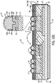
- POL structure 10 also includes a diffusion barrier layer 28 that is applied about POL sub-module 14 of POL structure 10.
- diffusion barrier layer 28 is configured to have a low permeability of moisture and gases (e.g., oxygen), so as to significantly reduce the amount of moisture and gases that are absorbed by the materials in the POL sub-module 14, underfill material 26, and at the interfaces between materials in the sub-module, as well as prevent other contaminants from coming in contact with the POL sub-module 14.
- the barrier layer 28 makes the POL structure 10 more reliable to soldering operations (e.g., soldering of second-level I/O connections 16 to a PCB).
- the diffusion barrier layer 28 is applied adjacent to second-level I/O connections 16 and is applied with a thickness that does not inhibit the soldering of the second-level I/O connections 16 to a PCB. Application of the diffusion barrier layer 28 to POL structure 10 according to various embodiments of the invention is discussed in greater detail below.
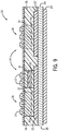
- FIGS. 2-12 detailed views of the process steps for a technique of manufacturing the POL structure 10 of FIG. 1 are provided, according to an embodiment of the invention.
- process steps for a build-up of the POL sub-module 14 are provided.
- the build-up process of POL sub-module 14 begins with the placement and attachment of a dielectric layer 30 or "flex layer” onto a frame structure 32.
- the dielectric layer 30 is in the form of a lamination or film and is placed on frame structure 32 to provide stability during the build-up process of POL sub-module 14.
- the dielectric layer 30 may be formed of one a plurality of dielectric materials, such as Kapton®, Ultem®, polytetrafluoroethylene (PTFE), Upilex®, polysulfone materials (e.g., Udel®, Radel®), or another polymer film, such as a liquid crystal polymer (LCP) or a polyimide material.
- dielectric materials such as Kapton®, Ultem®, polytetrafluoroethylene (PTFE), Upilex®, polysulfone materials (e.g., Udel®, Radel®), or another polymer film, such as a liquid crystal polymer (LCP) or a polyimide material.
- an adhesive layer 34 is deposited onto dielectric layer 30.
- a plurality of vias 36 is then formed through the adhesive layer 34 and dielectric layer 30, as illustrated in FIG. 4 .
- the vias 36 may be formed by way of a laser ablation or laser drilling process, plasma etching, photo-definition, or mechanical drilling processes.
- one or more semiconductor devices 12 e.g., three semiconductor devices are secured to dielectric layer 30 by way of adhesive layer 34, as illustrated in FIG. 5 .
- semiconductor devices 12 may be of varying thickness/height.
- a copper shim 37 may be soldered to one or more of semiconductor devices 12 in order to increase its thickness/height so that the thickness/height of all semiconductor devices 12 is equal and a back surface of the semiconductor devices 12 is "planarized.”
- vias 36 through adhesive layer 34 and dielectric lamination 30 is shown in FIG. 4 as being performed prior to placement of semiconductor devices 12 onto adhesive layer 34, it is recognized that the placement of semiconductor devices 12 could occur prior to via formation. That is, depending on constraints imposed by via size, semiconductor devices 12 could first be placed on adhesive layer 34 and dielectric layer 30, with the vias 36 subsequently being formed at locations corresponding to a plurality of metalized circuits and/or connection pads (not shown) formed on semiconductor devices 12. Furthermore, a combination of pre- and post-drilled vias could be employed as needed.
- first-level interconnects 38 are typically formed through a combination of sputtering and electroplating applications, although it is recognized that other electroless methods of metal deposition could also be used.
- a titanium adhesion layer and copper seed layer may first be applied via a sputtering process, followed by an electroplating process that increases a thickness of the copper to a desired level.
- metal interconnects 38 i.e., first level interconnects
- the metal interconnects 38 extend out from circuits and/or connection pads (not shown) of semiconductor devices 12, through vias/opening 36, and out across a top surface 39 of dielectric layer 30.
- POL sub-module 14 is attached to substrate structure 18 by way of a solder material 40, so as to secure the POL sub-module 14 and substrate structure 18 together. That is, each of semiconductor devices 12 is soldered to the die side DBC layer 22.
- a polymeric underfill, encapsulate, or molding compound 26 e.g., epoxy or other organic filler material
- diffusion barrier layer 28 is applied to the POL structure 10 to significantly reduce the amount of moisture and gases that are absorbed by the materials in the POL structure 10 and at the interfaces between materials in the structure, as well as prevent other contaminants from coming in contact with the POL sub-module 14.
- the diffusion barrier layer 28 may include organic materials, inorganic materials, ceramic materials, and any combination thereof, with these materials typically being reaction or recombination products of reacting plasma species.
- the layer forming diffusion barrier layer 28 has a low diffusion/transmission of moisture and gas therethrough so as to collectively reduce moisture and gas ingress into the POL structure 10.
- the diffusion barrier layer 28 may be applied via any of a number of suitable processes, such as a plasma-enhanced chemical vapor deposition process, and has a desired thickness, such as a thickness in the range of one atomic layer up to 25-100 microns, such that the layer 28 does not interfere with the solderability of the LGA/BGA solder bumps 17.
- the diffusion barrier layer 28 is configured as an electrically non-conductive layer that is applied at a low temperature, such as a temperature that does not exceed approximately 250-300 degrees Celsius, for example.
- solder mask layer 42 is applied over the patterned metal interconnects 38 on POL sub-module 14 to provide a protective coating for the copper shims thereof.
- the layer 42 could be composed of some metal material other than solder, such as Ni or Ni/Au.
- the second-level I/O interconnections 16 are then applied to solder mask 42 on top of the dielectric layer 30.
- I/O interconnections 16 are formed as LGA or BGA solder bumps 17 that are soldered to solder mask 42 to enable surface mounting of the POL structure 10 to an external circuit, with the solder bumps 17 providing a highly reliable second-level interconnection structure that is resistive to failure in high stress conditions.
- diffusion barrier layer 28 is then applied to the POL structure 10. The diffusion barrier layer 28 is applied over solder mask 42 and the solder bumps 17 of second-level I/O interconnection 16, without any need for patterning the layer.
- the diffusion barrier layer 28 also extends down the sides of the POL structure 10 and to the ceramic layer 20 or backside DBC layer 24, such that the underfill material 26 is also covered by the diffusion barrier layer 28 and the POL structure 10 is enclosed by the barrier layer 28.
- diffusion barrier layer 28 is applied to the POL structure 10 directly onto the metal interconnects 38.
- a solder mask layer 42 is then applied over the diffusion barrier layer 28 to provide a protective coating for the copper shims thereof, with the solder mask layer 42 also being used to etch the diffusion barrier layer 28 to open at locations where the LGA solder bumps 17 are to be formed.
- the second-level I/O interconnections 16 are applied to solder mask 42, on top of the dielectric layer 30 and on top of diffusion barrier layer 28, with the interconnections being in the form of LGA or BGA solder bumps 17 that are soldered to solder mask 42 to enable surface mounting of the POL structure 10 to an external circuit.
- the diffusion barrier layer 28 extends down the sides of the POL structure 10 and to the ceramic layer 20 or backside DBC layer 24, such that the underfill material 26 is also covered by the diffusion barrier layer 28 and the POL structure 10 is enclosed by the barrier layer.
- multiple diffusion barrier layers 28 are applied onto POL structure 10 at various stages of the manufacturing process. That is, a first diffusion barrier layer 28A is applied to the POL structure 10 directly onto the metal interconnects 38. A solder mask layer 42 is then applied over the diffusion barrier layer 28A to provide a protective coating for the copper shims thereof, with the second-level I/O interconnections 16 then being applied to solder mask 42 on top of the dielectric layer 30 and on top of the first diffusion barrier layer 28A, with the interconnections being in the form of LGA or BGA solder bumps 17.
- a second diffusion barrier layer 28B is then applied to the sub-module, with the second diffusion barrier layer 28B being applied over solder mask 42 and the solder bumps 17 of second-level I/O interconnection 16, without any need for patterning the layer.
- the second diffusion barrier layer 28B is configured such that the layer does not interfere with the solderability of the LGA/BGA solder bumps 17.
- the first and/or second diffusion barrier layers 28A, 28B extend down the sides of the POL structure and to the ceramic layer 20 or backside DBC layer 24, such that the underfill material 26 is also covered by the diffusion barrier layer and the POL structure 10 is enclosed by the barrier layer.
- diffusion barrier layer 28 is applied to the POL structure 10 directly onto the metal interconnects 38 and is configured to act as a solder mask.
- a thickness of diffusion barrier layer 28 is increased such that the barrier layer provides adequate protection to metal interconnects 38.
- the second-level I/O interconnections 16 are formed thereover, with the interconnections being in the form of LGA or BGA solder bumps 17.
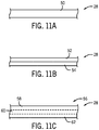
- FIGS. 11A-11C various examples diffusion barrier layers 28 are shown.
- FIG. 11C illustrates a diffusion barrier layer which is used in the surface mount package structure of the present invention.
- FIGS. 11A and 11B illustrate alternative diffusion barrier layers which are not used in the surface mount package of the present invention.
- the diffusion barrier layer 28 described with reference to FIGS. 11A-11C includes one or more layers formed of organic materials, inorganic materials, ceramic materials, and any combination thereof, with these materials typically being reaction or recombination products of reacting plasma species.
- the diffusion barrier layer 28 may be constructed as a single layer 50 having a consistent composition throughout.
- the single layer 50 may be formed of inorganic and/or ceramic materials only, with the inorganic/ceramic materials comprising any of oxides, nitrides, carbides, and borides of elements of Groups IIA, IIIA, IVA, VA, VIA, VIIA, IB, IIB, metals of Groups IIIB, IVB, VB, rare earth elements, or any combination thereof.
- the diffusion barrier layer 28 may instead be constructed as a stack of layers 52, 54 (i.e., a multi-layer construction), such as a first layer 52 and a second layer 54, although it is recognized that additional layers could be constructed.
- the first layer 52 may be formed of one or more organic materials, such as carbon, hydrogen, oxygen, and optionally other minor elements, such as sulfur, nitrogen, silicon, etc., depending on the types of reactants used therewith, with suitable reactants that result in organic compositions in the coating being straight or branched alkanes, alkenes, alkynes, alcohols, aldehydes, ethers, alkylene oxides, aromatics, etc., having up to 15 carbon atoms.
- the second layer 54 may be formed of inorganic and/or ceramic materials, with the inorganic/ceramic materials comprising any of oxides, nitrides, carbides, and borides of elements of Groups IIA, IIIA, IVA, VA, VIA, VIIA, IB, IIB, metals of Groups IIIB, IVB, VB, rare earth elements, or any combination thereof.
- the diffusion barrier layer 28 may be constructed as a layer 56 having a graded composition, i.e., the composition of the layer 56 varies across a thickness of the layer, such that layer 56 can be termed as having a plurality of regions 58, 60, 62.
- Suitable coating compositions of regions 58, 60, 62 across the thickness of layer 56 are organic, inorganic, or ceramic materials, such as the organic, inorganic, and ceramic materials set forth above.
- silicon carbide can be deposited onto a substrate by recombination of plasmas generated from silane (SiH 4 ) and an organic material, such as methane or xylene.
- Silicon oxycarbide can be deposited from plasmas generated from silane, methane, and oxygen or silane and propylene oxide. Silicon oxycarbide also can be deposited from plasmas generated from organosilicone precursors, such as tetraethoxysilane (TEOS), hexamethyldisiloxane (HMDSO), hexamethyldisilazane (HMDSN), or octamethylcyclotetrasiloxane (D 4 ). Silicon nitride can be deposited from plasmas generated from silane and ammonia. Aluminum oxycarbonitride can be deposited from a plasma generated from a mixture of aluminum tartrate and ammonia. Other combinations of reactants may be chosen to obtain a desired composition of layer 56. A graded composition of the layer 56 is obtained by changing the compositions of the reactants fed into the reactor chamber during the deposition of reaction products to form the layer.
- organosilicone precursors such as tetraethoxysilane (TE
- embodiments of the invention thus provide a POL packaging and interconnect structure 10 having second-level package I/O's 16 that are provided on the flex side (i.e., on top of dielectric layer 30) of the POL sub-module 14 for second-level interconnection to an external circuit and the entire non-die side DBC layer 24 is available for thermal connection.
- the POL structure 10 includes a diffusion barrier layer 28 configured to reduce the ingress of moisture and gases into the package, so as to provide enhanced reliability to moisture and gas related failure mechanisms.
- the diffusion barrier layer 28 is further configured such that it does not interfere with the solderability of the second-level I/O interconnections 16 to a PCB or other external circuit.
Landscapes
- Non-Metallic Protective Coatings For Printed Circuits (AREA)
- Wire Bonding (AREA)
- Engineering & Computer Science (AREA)
- Production Of Multi-Layered Print Wiring Board (AREA)
- Structures Or Materials For Encapsulating Or Coating Semiconductor Devices Or Solid State Devices (AREA)
- Manufacturing & Machinery (AREA)
- Chemical & Material Sciences (AREA)
- Ceramic Engineering (AREA)
- Microelectronics & Electronic Packaging (AREA)
Applications Claiming Priority (1)
| Application Number | Priority Date | Filing Date | Title |
|---|---|---|---|
| US13/561,868 US9299630B2 (en) | 2012-07-30 | 2012-07-30 | Diffusion barrier for surface mount modules |
Publications (3)
| Publication Number | Publication Date |
|---|---|
| EP2693470A2 EP2693470A2 (en) | 2014-02-05 |
| EP2693470A3 EP2693470A3 (en) | 2015-07-22 |
| EP2693470B1 true EP2693470B1 (en) | 2020-10-28 |
Family
ID=48803437
Family Applications (1)
| Application Number | Title | Priority Date | Filing Date |
|---|---|---|---|
| EP13177219.6A Active EP2693470B1 (en) | 2012-07-30 | 2013-07-19 | Surface mount module with diffusion barrier and method of making the same |
Country Status (7)
| Country | Link |
|---|---|
| US (1) | US9299630B2 (https=) |
| EP (1) | EP2693470B1 (https=) |
| JP (1) | JP6266251B2 (https=) |
| KR (1) | KR102089926B1 (https=) |
| CN (1) | CN103579136B (https=) |
| SG (2) | SG196754A1 (https=) |
| TW (1) | TWI588957B (https=) |
Families Citing this family (22)
| Publication number | Priority date | Publication date | Assignee | Title |
|---|---|---|---|---|
| US10269688B2 (en) | 2013-03-14 | 2019-04-23 | General Electric Company | Power overlay structure and method of making same |
| US8987876B2 (en) * | 2013-03-14 | 2015-03-24 | General Electric Company | Power overlay structure and method of making same |
| KR102117477B1 (ko) * | 2015-04-23 | 2020-06-01 | 삼성전기주식회사 | 반도체 패키지 및 반도체 패키지의 제조방법 |
| US9711713B1 (en) * | 2016-01-15 | 2017-07-18 | Taiwan Semiconductor Manufacturing Company Ltd. | Semiconductor structure, electrode structure and method of forming the same |
| US10453786B2 (en) | 2016-01-19 | 2019-10-22 | General Electric Company | Power electronics package and method of manufacturing thereof |
| CN205807211U (zh) * | 2016-06-20 | 2016-12-14 | 冯霞 | 用于容器的发光装置 |
| FR3061404B1 (fr) * | 2016-12-27 | 2022-09-23 | Packaging Sip | Procede de fabrication collective de modules electroniques hermetiques |
| US10804115B2 (en) | 2017-08-03 | 2020-10-13 | General Electric Company | Electronics package with integrated interconnect structure and method of manufacturing thereof |
| US10541153B2 (en) | 2017-08-03 | 2020-01-21 | General Electric Company | Electronics package with integrated interconnect structure and method of manufacturing thereof |
| US10541209B2 (en) | 2017-08-03 | 2020-01-21 | General Electric Company | Electronics package including integrated electromagnetic interference shield and method of manufacturing thereof |
| US10332832B2 (en) | 2017-08-07 | 2019-06-25 | General Electric Company | Method of manufacturing an electronics package using device-last or device-almost last placement |
| US10685935B2 (en) * | 2017-11-15 | 2020-06-16 | Taiwan Semiconductor Manufacturing Company, Ltd. | Forming metal bonds with recesses |
| CN108044259B (zh) * | 2017-12-01 | 2020-04-03 | 温州宏丰电工合金股份有限公司 | 一种用于不锈钢真空钎焊的阻流剂的制备方法 |
| CN108098093B (zh) * | 2017-12-01 | 2020-04-03 | 温州宏丰电工合金股份有限公司 | 一种用于不锈钢真空钎焊的阻流剂 |
| EP3518278A1 (en) * | 2018-01-30 | 2019-07-31 | Infineon Technologies AG | Power semiconductor module and method for producing the same |
| CN111819682B (zh) * | 2018-03-26 | 2025-04-29 | 三菱综合材料株式会社 | 绝缘电路基板用接合体的制造方法及绝缘电路基板用接合体 |
| US10892237B2 (en) * | 2018-12-14 | 2021-01-12 | General Electric Company | Methods of fabricating high voltage semiconductor devices having improved electric field suppression |
| US11538769B2 (en) | 2018-12-14 | 2022-12-27 | General Electric Company | High voltage semiconductor devices having improved electric field suppression |
| US11398445B2 (en) | 2020-05-29 | 2022-07-26 | General Electric Company | Mechanical punched via formation in electronics package and electronics package formed thereby |
| JPWO2023190106A1 (https=) * | 2022-03-31 | 2023-10-05 | ||
| WO2023190107A1 (ja) * | 2022-03-31 | 2023-10-05 | 株式会社Flosfia | 半導体装置 |
| US12362237B1 (en) * | 2024-04-05 | 2025-07-15 | Wolfspeed, Inc. | Fill-in planarization system and method |
Citations (1)
| Publication number | Priority date | Publication date | Assignee | Title |
|---|---|---|---|---|
| US20040046497A1 (en) * | 2002-09-11 | 2004-03-11 | General Electric Company | Diffusion barrier coatings having graded compositions and devices incorporating the same |
Family Cites Families (22)
| Publication number | Priority date | Publication date | Assignee | Title |
|---|---|---|---|---|
| US5250843A (en) | 1991-03-27 | 1993-10-05 | Integrated System Assemblies Corp. | Multichip integrated circuit modules |
| TW272311B (https=) * | 1994-01-12 | 1996-03-11 | At & T Corp | |
| US7653215B2 (en) * | 1997-04-02 | 2010-01-26 | Gentex Corporation | System for controlling exterior vehicle lights |
| US6306680B1 (en) | 1999-02-22 | 2001-10-23 | General Electric Company | Power overlay chip scale packages for discrete power devices |
| US6154366A (en) | 1999-11-23 | 2000-11-28 | Intel Corporation | Structures and processes for fabricating moisture resistant chip-on-flex packages |
| US6551148B1 (en) * | 2001-10-19 | 2003-04-22 | Hewlett-Packard Development Company, L.P. | Electrical connector with minimized non-target contact |
| US7169345B2 (en) * | 2003-08-27 | 2007-01-30 | Texas Instruments Incorporated | Method for integrated circuit packaging |
| WO2005051525A1 (en) | 2003-11-25 | 2005-06-09 | Polyvalor, Limited Partnership | Permeation barrier coating or layer with modulated properties and methods of making the same |
| US7262444B2 (en) * | 2005-08-17 | 2007-08-28 | General Electric Company | Power semiconductor packaging method and structure |
| US8018056B2 (en) * | 2005-12-21 | 2011-09-13 | International Rectifier Corporation | Package for high power density devices |
| US7733554B2 (en) | 2006-03-08 | 2010-06-08 | E Ink Corporation | Electro-optic displays, and materials and methods for production thereof |
| US20070295387A1 (en) | 2006-05-05 | 2007-12-27 | Nanosolar, Inc. | Solar assembly with a multi-ply barrier layer and individually encapsulated solar cells or solar cell strings |
| US7688497B2 (en) | 2007-01-22 | 2010-03-30 | E Ink Corporation | Multi-layer sheet for use in electro-optic displays |
| US9953910B2 (en) * | 2007-06-21 | 2018-04-24 | General Electric Company | Demountable interconnect structure |
| JP5241177B2 (ja) * | 2007-09-05 | 2013-07-17 | 株式会社オクテック | 半導体装置及び半導体装置の製造方法 |
| US20100308468A1 (en) * | 2008-03-14 | 2010-12-09 | Noriyuki Yoshikawa | Semiconductor device and semiconductor device fabrication method |
| DE102008028757B4 (de) * | 2008-06-17 | 2017-03-16 | Epcos Ag | Verfahren zur Herstellung einer Halbleiterchipanordnung |
| US8358000B2 (en) * | 2009-03-13 | 2013-01-22 | General Electric Company | Double side cooled power module with power overlay |
| US9013018B2 (en) | 2010-02-18 | 2015-04-21 | Beneq Oy | Multilayer moisture barrier |
| JP2010212698A (ja) * | 2010-04-01 | 2010-09-24 | Sony Chemical & Information Device Corp | 接続構造体及びその製造方法 |
| US8531027B2 (en) * | 2010-04-30 | 2013-09-10 | General Electric Company | Press-pack module with power overlay interconnection |
| US8114712B1 (en) * | 2010-12-22 | 2012-02-14 | General Electric Company | Method for fabricating a semiconductor device package |
-
2012
- 2012-07-30 US US13/561,868 patent/US9299630B2/en active Active
-
2013
- 2013-07-15 TW TW102125294A patent/TWI588957B/zh active
- 2013-07-19 EP EP13177219.6A patent/EP2693470B1/en active Active
- 2013-07-25 SG SG2013056924A patent/SG196754A1/en unknown
- 2013-07-25 SG SG10201508888UA patent/SG10201508888UA/en unknown
- 2013-07-26 JP JP2013155115A patent/JP6266251B2/ja active Active
- 2013-07-29 KR KR1020130089684A patent/KR102089926B1/ko active Active
- 2013-07-30 CN CN201310324406.0A patent/CN103579136B/zh active Active
Patent Citations (1)
| Publication number | Priority date | Publication date | Assignee | Title |
|---|---|---|---|---|
| US20040046497A1 (en) * | 2002-09-11 | 2004-03-11 | General Electric Company | Diffusion barrier coatings having graded compositions and devices incorporating the same |
Also Published As
| Publication number | Publication date |
|---|---|
| EP2693470A2 (en) | 2014-02-05 |
| EP2693470A3 (en) | 2015-07-22 |
| JP6266251B2 (ja) | 2018-01-24 |
| US9299630B2 (en) | 2016-03-29 |
| KR20140016192A (ko) | 2014-02-07 |
| TWI588957B (zh) | 2017-06-21 |
| CN103579136A (zh) | 2014-02-12 |
| CN103579136B (zh) | 2018-03-06 |
| US20140029210A1 (en) | 2014-01-30 |
| TW201409635A (zh) | 2014-03-01 |
| KR102089926B1 (ko) | 2020-04-14 |
| JP2014027277A (ja) | 2014-02-06 |
| SG196754A1 (en) | 2014-02-13 |
| SG10201508888UA (en) | 2015-11-27 |
Similar Documents
| Publication | Publication Date | Title |
|---|---|---|
| EP2693470B1 (en) | Surface mount module with diffusion barrier and method of making the same | |
| US9184124B2 (en) | Reliable surface mount integrated power module | |
| US11177204B2 (en) | Power electronics package and method of manufacturing thereof | |
| US10186477B2 (en) | Power overlay structure and method of making same | |
| CN102956594B (zh) | 带有引线框连接的功率覆盖结构 | |
| CN108428689B (zh) | 功率电子设备组件及其制造方法 | |
| TWI697077B (zh) | 功率電子封裝及其製造方法 | |
| KR100836657B1 (ko) | 전자 패키지 및 그 제조방법 | |
| KR20180092379A (ko) | 전력 전자 패키지 및 그 제조 방법 |
Legal Events
| Date | Code | Title | Description |
|---|---|---|---|
| AK | Designated contracting states |
Kind code of ref document: A2 Designated state(s): AL AT BE BG CH CY CZ DE DK EE ES FI FR GB GR HR HU IE IS IT LI LT LU LV MC MK MT NL NO PL PT RO RS SE SI SK SM TR |
|
| AX | Request for extension of the european patent |
Extension state: BA ME |
|
| PUAI | Public reference made under article 153(3) epc to a published international application that has entered the european phase |
Free format text: ORIGINAL CODE: 0009012 |
|
| PUAL | Search report despatched |
Free format text: ORIGINAL CODE: 0009013 |
|
| AK | Designated contracting states |
Kind code of ref document: A3 Designated state(s): AL AT BE BG CH CY CZ DE DK EE ES FI FR GB GR HR HU IE IS IT LI LT LU LV MC MK MT NL NO PL PT RO RS SE SI SK SM TR |
|
| AX | Request for extension of the european patent |
Extension state: BA ME |
|
| RIC1 | Information provided on ipc code assigned before grant |
Ipc: H01L 23/00 20060101ALI20150618BHEP Ipc: H01L 23/498 20060101ALI20150618BHEP Ipc: H01L 23/538 20060101ALI20150618BHEP Ipc: H01L 23/31 20060101AFI20150618BHEP Ipc: H01L 23/532 20060101ALI20150618BHEP Ipc: H01L 21/56 20060101ALN20150618BHEP Ipc: H01L 23/373 20060101ALI20150618BHEP Ipc: H01L 21/48 20060101ALI20150618BHEP |
|
| 17P | Request for examination filed |
Effective date: 20160122 |
|
| RBV | Designated contracting states (corrected) |
Designated state(s): AL AT BE BG CH CY CZ DE DK EE ES FI FR GB GR HR HU IE IS IT LI LT LU LV MC MK MT NL NO PL PT RO RS SE SI SK SM TR |
|
| STAA | Information on the status of an ep patent application or granted ep patent |
Free format text: STATUS: EXAMINATION IS IN PROGRESS |
|
| 17Q | First examination report despatched |
Effective date: 20180425 |
|
| GRAP | Despatch of communication of intention to grant a patent |
Free format text: ORIGINAL CODE: EPIDOSNIGR1 |
|
| RIC1 | Information provided on ipc code assigned before grant |
Ipc: H01L 23/532 20060101ALI20200608BHEP Ipc: H01L 21/48 20060101ALI20200608BHEP Ipc: H01L 23/00 20060101ALI20200608BHEP Ipc: H01L 23/31 20060101AFI20200608BHEP Ipc: H01L 23/498 20060101ALI20200608BHEP Ipc: H01L 21/56 20060101ALN20200608BHEP Ipc: H01L 23/538 20060101ALI20200608BHEP Ipc: H01L 23/373 20060101ALI20200608BHEP |
|
| STAA | Information on the status of an ep patent application or granted ep patent |
Free format text: STATUS: GRANT OF PATENT IS INTENDED |
|
| RIC1 | Information provided on ipc code assigned before grant |
Ipc: H01L 23/538 20060101ALI20200616BHEP Ipc: H01L 23/532 20060101ALI20200616BHEP Ipc: H01L 23/373 20060101ALI20200616BHEP Ipc: H01L 21/56 20060101ALN20200616BHEP Ipc: H01L 21/48 20060101ALI20200616BHEP Ipc: H01L 23/00 20060101ALI20200616BHEP Ipc: H01L 23/31 20060101AFI20200616BHEP Ipc: H01L 23/498 20060101ALI20200616BHEP |
|
| INTG | Intention to grant announced |
Effective date: 20200716 |
|
| RIC1 | Information provided on ipc code assigned before grant |
Ipc: H01L 23/538 20060101ALI20200706BHEP Ipc: H01L 23/373 20060101ALI20200706BHEP Ipc: H01L 23/00 20060101ALI20200706BHEP Ipc: H01L 21/48 20060101ALI20200706BHEP Ipc: H01L 23/31 20060101AFI20200706BHEP Ipc: H01L 23/498 20060101ALI20200706BHEP Ipc: H01L 23/532 20060101ALI20200706BHEP Ipc: H01L 21/56 20060101ALN20200706BHEP |
|
| RIN1 | Information on inventor provided before grant (corrected) |
Inventor name: ZHAO, RI-AN Inventor name: MCCONNELEE, PAUL ALAN Inventor name: CHAUHAN, SHAKTI SINGH Inventor name: GOWDA, ARUN VIRUPAKSHA |
|
| GRAS | Grant fee paid |
Free format text: ORIGINAL CODE: EPIDOSNIGR3 |
|
| GRAA | (expected) grant |
Free format text: ORIGINAL CODE: 0009210 |
|
| STAA | Information on the status of an ep patent application or granted ep patent |
Free format text: STATUS: THE PATENT HAS BEEN GRANTED |
|
| AK | Designated contracting states |
Kind code of ref document: B1 Designated state(s): AL AT BE BG CH CY CZ DE DK EE ES FI FR GB GR HR HU IE IS IT LI LT LU LV MC MK MT NL NO PL PT RO RS SE SI SK SM TR |
|
| REG | Reference to a national code |
Ref country code: GB Ref legal event code: FG4D |
|
| REG | Reference to a national code |
Ref country code: CH Ref legal event code: EP |
|
| REG | Reference to a national code |
Ref country code: DE Ref legal event code: R096 Ref document number: 602013073566 Country of ref document: DE |
|
| REG | Reference to a national code |
Ref country code: AT Ref legal event code: REF Ref document number: 1329078 Country of ref document: AT Kind code of ref document: T Effective date: 20201115 |
|
| REG | Reference to a national code |
Ref country code: IE Ref legal event code: FG4D |
|
| REG | Reference to a national code |
Ref country code: AT Ref legal event code: MK05 Ref document number: 1329078 Country of ref document: AT Kind code of ref document: T Effective date: 20201028 |
|
| REG | Reference to a national code |
Ref country code: NL Ref legal event code: MP Effective date: 20201028 |
|
| PG25 | Lapsed in a contracting state [announced via postgrant information from national office to epo] |
Ref country code: GR Free format text: LAPSE BECAUSE OF FAILURE TO SUBMIT A TRANSLATION OF THE DESCRIPTION OR TO PAY THE FEE WITHIN THE PRESCRIBED TIME-LIMIT Effective date: 20210129 Ref country code: FI Free format text: LAPSE BECAUSE OF FAILURE TO SUBMIT A TRANSLATION OF THE DESCRIPTION OR TO PAY THE FEE WITHIN THE PRESCRIBED TIME-LIMIT Effective date: 20201028 Ref country code: RS Free format text: LAPSE BECAUSE OF FAILURE TO SUBMIT A TRANSLATION OF THE DESCRIPTION OR TO PAY THE FEE WITHIN THE PRESCRIBED TIME-LIMIT Effective date: 20201028 Ref country code: NO Free format text: LAPSE BECAUSE OF FAILURE TO SUBMIT A TRANSLATION OF THE DESCRIPTION OR TO PAY THE FEE WITHIN THE PRESCRIBED TIME-LIMIT Effective date: 20210128 Ref country code: PT Free format text: LAPSE BECAUSE OF FAILURE TO SUBMIT A TRANSLATION OF THE DESCRIPTION OR TO PAY THE FEE WITHIN THE PRESCRIBED TIME-LIMIT Effective date: 20210301 Ref country code: NL Free format text: LAPSE BECAUSE OF FAILURE TO SUBMIT A TRANSLATION OF THE DESCRIPTION OR TO PAY THE FEE WITHIN THE PRESCRIBED TIME-LIMIT Effective date: 20201028 |
|
| REG | Reference to a national code |
Ref country code: LT Ref legal event code: MG4D |
|
| PG25 | Lapsed in a contracting state [announced via postgrant information from national office to epo] |
Ref country code: BG Free format text: LAPSE BECAUSE OF FAILURE TO SUBMIT A TRANSLATION OF THE DESCRIPTION OR TO PAY THE FEE WITHIN THE PRESCRIBED TIME-LIMIT Effective date: 20210128 Ref country code: AT Free format text: LAPSE BECAUSE OF FAILURE TO SUBMIT A TRANSLATION OF THE DESCRIPTION OR TO PAY THE FEE WITHIN THE PRESCRIBED TIME-LIMIT Effective date: 20201028 Ref country code: ES Free format text: LAPSE BECAUSE OF FAILURE TO SUBMIT A TRANSLATION OF THE DESCRIPTION OR TO PAY THE FEE WITHIN THE PRESCRIBED TIME-LIMIT Effective date: 20201028 Ref country code: SE Free format text: LAPSE BECAUSE OF FAILURE TO SUBMIT A TRANSLATION OF THE DESCRIPTION OR TO PAY THE FEE WITHIN THE PRESCRIBED TIME-LIMIT Effective date: 20201028 Ref country code: PL Free format text: LAPSE BECAUSE OF FAILURE TO SUBMIT A TRANSLATION OF THE DESCRIPTION OR TO PAY THE FEE WITHIN THE PRESCRIBED TIME-LIMIT Effective date: 20201028 Ref country code: LV Free format text: LAPSE BECAUSE OF FAILURE TO SUBMIT A TRANSLATION OF THE DESCRIPTION OR TO PAY THE FEE WITHIN THE PRESCRIBED TIME-LIMIT Effective date: 20201028 Ref country code: IS Free format text: LAPSE BECAUSE OF FAILURE TO SUBMIT A TRANSLATION OF THE DESCRIPTION OR TO PAY THE FEE WITHIN THE PRESCRIBED TIME-LIMIT Effective date: 20210228 |
|
| PG25 | Lapsed in a contracting state [announced via postgrant information from national office to epo] |
Ref country code: HR Free format text: LAPSE BECAUSE OF FAILURE TO SUBMIT A TRANSLATION OF THE DESCRIPTION OR TO PAY THE FEE WITHIN THE PRESCRIBED TIME-LIMIT Effective date: 20201028 |
|
| REG | Reference to a national code |
Ref country code: DE Ref legal event code: R097 Ref document number: 602013073566 Country of ref document: DE |
|
| PG25 | Lapsed in a contracting state [announced via postgrant information from national office to epo] |
Ref country code: SK Free format text: LAPSE BECAUSE OF FAILURE TO SUBMIT A TRANSLATION OF THE DESCRIPTION OR TO PAY THE FEE WITHIN THE PRESCRIBED TIME-LIMIT Effective date: 20201028 Ref country code: RO Free format text: LAPSE BECAUSE OF FAILURE TO SUBMIT A TRANSLATION OF THE DESCRIPTION OR TO PAY THE FEE WITHIN THE PRESCRIBED TIME-LIMIT Effective date: 20201028 Ref country code: LT Free format text: LAPSE BECAUSE OF FAILURE TO SUBMIT A TRANSLATION OF THE DESCRIPTION OR TO PAY THE FEE WITHIN THE PRESCRIBED TIME-LIMIT Effective date: 20201028 Ref country code: EE Free format text: LAPSE BECAUSE OF FAILURE TO SUBMIT A TRANSLATION OF THE DESCRIPTION OR TO PAY THE FEE WITHIN THE PRESCRIBED TIME-LIMIT Effective date: 20201028 Ref country code: CZ Free format text: LAPSE BECAUSE OF FAILURE TO SUBMIT A TRANSLATION OF THE DESCRIPTION OR TO PAY THE FEE WITHIN THE PRESCRIBED TIME-LIMIT Effective date: 20201028 Ref country code: SM Free format text: LAPSE BECAUSE OF FAILURE TO SUBMIT A TRANSLATION OF THE DESCRIPTION OR TO PAY THE FEE WITHIN THE PRESCRIBED TIME-LIMIT Effective date: 20201028 |
|
| PG25 | Lapsed in a contracting state [announced via postgrant information from national office to epo] |
Ref country code: DK Free format text: LAPSE BECAUSE OF FAILURE TO SUBMIT A TRANSLATION OF THE DESCRIPTION OR TO PAY THE FEE WITHIN THE PRESCRIBED TIME-LIMIT Effective date: 20201028 |
|
| PLBE | No opposition filed within time limit |
Free format text: ORIGINAL CODE: 0009261 |
|
| STAA | Information on the status of an ep patent application or granted ep patent |
Free format text: STATUS: NO OPPOSITION FILED WITHIN TIME LIMIT |
|
| 26N | No opposition filed |
Effective date: 20210729 |
|
| PG25 | Lapsed in a contracting state [announced via postgrant information from national office to epo] |
Ref country code: IT Free format text: LAPSE BECAUSE OF FAILURE TO SUBMIT A TRANSLATION OF THE DESCRIPTION OR TO PAY THE FEE WITHIN THE PRESCRIBED TIME-LIMIT Effective date: 20201028 Ref country code: AL Free format text: LAPSE BECAUSE OF FAILURE TO SUBMIT A TRANSLATION OF THE DESCRIPTION OR TO PAY THE FEE WITHIN THE PRESCRIBED TIME-LIMIT Effective date: 20201028 |
|
| PG25 | Lapsed in a contracting state [announced via postgrant information from national office to epo] |
Ref country code: SI Free format text: LAPSE BECAUSE OF FAILURE TO SUBMIT A TRANSLATION OF THE DESCRIPTION OR TO PAY THE FEE WITHIN THE PRESCRIBED TIME-LIMIT Effective date: 20201028 |
|
| REG | Reference to a national code |
Ref country code: CH Ref legal event code: PL |
|
| PG25 | Lapsed in a contracting state [announced via postgrant information from national office to epo] |
Ref country code: MC Free format text: LAPSE BECAUSE OF FAILURE TO SUBMIT A TRANSLATION OF THE DESCRIPTION OR TO PAY THE FEE WITHIN THE PRESCRIBED TIME-LIMIT Effective date: 20201028 |
|
| REG | Reference to a national code |
Ref country code: BE Ref legal event code: MM Effective date: 20210731 |
|
| PG25 | Lapsed in a contracting state [announced via postgrant information from national office to epo] |
Ref country code: LI Free format text: LAPSE BECAUSE OF NON-PAYMENT OF DUE FEES Effective date: 20210731 Ref country code: CH Free format text: LAPSE BECAUSE OF NON-PAYMENT OF DUE FEES Effective date: 20210731 |
|
| PG25 | Lapsed in a contracting state [announced via postgrant information from national office to epo] |
Ref country code: IS Free format text: LAPSE BECAUSE OF FAILURE TO SUBMIT A TRANSLATION OF THE DESCRIPTION OR TO PAY THE FEE WITHIN THE PRESCRIBED TIME-LIMIT Effective date: 20210228 Ref country code: LU Free format text: LAPSE BECAUSE OF NON-PAYMENT OF DUE FEES Effective date: 20210719 |
|
| PG25 | Lapsed in a contracting state [announced via postgrant information from national office to epo] |
Ref country code: IE Free format text: LAPSE BECAUSE OF NON-PAYMENT OF DUE FEES Effective date: 20210719 Ref country code: BE Free format text: LAPSE BECAUSE OF NON-PAYMENT OF DUE FEES Effective date: 20210731 |
|
| PG25 | Lapsed in a contracting state [announced via postgrant information from national office to epo] |
Ref country code: HU Free format text: LAPSE BECAUSE OF FAILURE TO SUBMIT A TRANSLATION OF THE DESCRIPTION OR TO PAY THE FEE WITHIN THE PRESCRIBED TIME-LIMIT; INVALID AB INITIO Effective date: 20130719 |
|
| PG25 | Lapsed in a contracting state [announced via postgrant information from national office to epo] |
Ref country code: CY Free format text: LAPSE BECAUSE OF FAILURE TO SUBMIT A TRANSLATION OF THE DESCRIPTION OR TO PAY THE FEE WITHIN THE PRESCRIBED TIME-LIMIT Effective date: 20201028 |
|
| PG25 | Lapsed in a contracting state [announced via postgrant information from national office to epo] |
Ref country code: MK Free format text: LAPSE BECAUSE OF FAILURE TO SUBMIT A TRANSLATION OF THE DESCRIPTION OR TO PAY THE FEE WITHIN THE PRESCRIBED TIME-LIMIT Effective date: 20201028 |
|
| PG25 | Lapsed in a contracting state [announced via postgrant information from national office to epo] |
Ref country code: MT Free format text: LAPSE BECAUSE OF FAILURE TO SUBMIT A TRANSLATION OF THE DESCRIPTION OR TO PAY THE FEE WITHIN THE PRESCRIBED TIME-LIMIT Effective date: 20201028 |
|
| PGFP | Annual fee paid to national office [announced via postgrant information from national office to epo] |
Ref country code: GB Payment date: 20250619 Year of fee payment: 13 |
|
| PGFP | Annual fee paid to national office [announced via postgrant information from national office to epo] |
Ref country code: FR Payment date: 20250620 Year of fee payment: 13 |
|
| PGFP | Annual fee paid to national office [announced via postgrant information from national office to epo] |
Ref country code: DE Payment date: 20250620 Year of fee payment: 13 |
|
| REG | Reference to a national code |
Ref country code: DE Ref legal event code: R079 Ref document number: 602013073566 Country of ref document: DE Free format text: PREVIOUS MAIN CLASS: H01L0023310000 Ipc: H10W0074100000 |
|
| PG25 | Lapsed in a contracting state [announced via postgrant information from national office to epo] |
Ref country code: TR Free format text: LAPSE BECAUSE OF FAILURE TO SUBMIT A TRANSLATION OF THE DESCRIPTION OR TO PAY THE FEE WITHIN THE PRESCRIBED TIME-LIMIT Effective date: 20201028 |