EP2693470B1 - Surface mount module with diffusion barrier and method of making the same - Google Patents
Surface mount module with diffusion barrier and method of making the same Download PDFInfo
- Publication number
- EP2693470B1 EP2693470B1 EP13177219.6A EP13177219A EP2693470B1 EP 2693470 B1 EP2693470 B1 EP 2693470B1 EP 13177219 A EP13177219 A EP 13177219A EP 2693470 B1 EP2693470 B1 EP 2693470B1
- Authority
- EP
- European Patent Office
- Prior art keywords
- layer
- diffusion barrier
- barrier layer
- level
- module
- Prior art date
- Legal status (The legal status is an assumption and is not a legal conclusion. Google has not performed a legal analysis and makes no representation as to the accuracy of the status listed.)
- Active
Links
- 230000004888 barrier function Effects 0.000 title claims description 78
- 238000009792 diffusion process Methods 0.000 title claims description 74
- 238000004519 manufacturing process Methods 0.000 title claims description 11
- 239000010410 layer Substances 0.000 claims description 184
- 239000004065 semiconductor Substances 0.000 claims description 49
- 229910000679 solder Inorganic materials 0.000 claims description 44
- 239000000758 substrate Substances 0.000 claims description 32
- 229910052751 metal Inorganic materials 0.000 claims description 28
- 239000002184 metal Substances 0.000 claims description 28
- 238000000034 method Methods 0.000 claims description 28
- 239000000463 material Substances 0.000 claims description 23
- 239000007789 gas Substances 0.000 claims description 14
- 239000010949 copper Substances 0.000 claims description 13
- RYGMFSIKBFXOCR-UHFFFAOYSA-N Copper Chemical compound [Cu] RYGMFSIKBFXOCR-UHFFFAOYSA-N 0.000 claims description 12
- 239000012790 adhesive layer Substances 0.000 claims description 12
- 229910052802 copper Inorganic materials 0.000 claims description 12
- 229910010272 inorganic material Inorganic materials 0.000 claims description 12
- 239000003989 dielectric material Substances 0.000 claims description 11
- 239000000203 mixture Substances 0.000 claims description 11
- 229910010293 ceramic material Inorganic materials 0.000 claims description 10
- 239000000919 ceramic Substances 0.000 claims description 9
- 239000011368 organic material Substances 0.000 claims description 9
- 239000011147 inorganic material Substances 0.000 claims description 6
- 150000001247 metal acetylides Chemical class 0.000 claims description 3
- 150000002739 metals Chemical class 0.000 claims description 3
- 150000004767 nitrides Chemical class 0.000 claims description 3
- 229910052761 rare earth metal Inorganic materials 0.000 claims description 3
- 230000008569 process Effects 0.000 description 13
- QVGXLLKOCUKJST-UHFFFAOYSA-N atomic oxygen Chemical compound [O] QVGXLLKOCUKJST-UHFFFAOYSA-N 0.000 description 7
- 229910052760 oxygen Inorganic materials 0.000 description 7
- 239000001301 oxygen Substances 0.000 description 7
- 210000002381 plasma Anatomy 0.000 description 7
- 238000004806 packaging method and process Methods 0.000 description 6
- BLRPTPMANUNPDV-UHFFFAOYSA-N Silane Chemical compound [SiH4] BLRPTPMANUNPDV-UHFFFAOYSA-N 0.000 description 5
- QGZKDVFQNNGYKY-UHFFFAOYSA-N Ammonia Chemical compound N QGZKDVFQNNGYKY-UHFFFAOYSA-N 0.000 description 4
- PNEYBMLMFCGWSK-UHFFFAOYSA-N aluminium oxide Inorganic materials [O-2].[O-2].[O-2].[Al+3].[Al+3] PNEYBMLMFCGWSK-UHFFFAOYSA-N 0.000 description 4
- 230000015572 biosynthetic process Effects 0.000 description 4
- 238000000151 deposition Methods 0.000 description 4
- 230000008021 deposition Effects 0.000 description 4
- 238000005516 engineering process Methods 0.000 description 4
- FFUAGWLWBBFQJT-UHFFFAOYSA-N hexamethyldisilazane Chemical compound C[Si](C)(C)N[Si](C)(C)C FFUAGWLWBBFQJT-UHFFFAOYSA-N 0.000 description 4
- 230000007774 longterm Effects 0.000 description 4
- VNWKTOKETHGBQD-UHFFFAOYSA-N methane Chemical compound C VNWKTOKETHGBQD-UHFFFAOYSA-N 0.000 description 4
- 238000000465 moulding Methods 0.000 description 4
- 239000000376 reactant Substances 0.000 description 4
- 229910000077 silane Inorganic materials 0.000 description 4
- 238000005476 soldering Methods 0.000 description 4
- XUIMIQQOPSSXEZ-UHFFFAOYSA-N Silicon Chemical compound [Si] XUIMIQQOPSSXEZ-UHFFFAOYSA-N 0.000 description 3
- 229910052782 aluminium Inorganic materials 0.000 description 3
- XAGFODPZIPBFFR-UHFFFAOYSA-N aluminium Chemical compound [Al] XAGFODPZIPBFFR-UHFFFAOYSA-N 0.000 description 3
- 239000011248 coating agent Substances 0.000 description 3
- 238000000576 coating method Methods 0.000 description 3
- 150000001875 compounds Chemical class 0.000 description 3
- 239000007769 metal material Substances 0.000 description 3
- 238000001020 plasma etching Methods 0.000 description 3
- 239000011253 protective coating Substances 0.000 description 3
- 230000006798 recombination Effects 0.000 description 3
- 238000005215 recombination Methods 0.000 description 3
- 239000010703 silicon Substances 0.000 description 3
- 229910052710 silicon Inorganic materials 0.000 description 3
- 238000003860 storage Methods 0.000 description 3
- IJGRMHOSHXDMSA-UHFFFAOYSA-N Atomic nitrogen Chemical compound N#N IJGRMHOSHXDMSA-UHFFFAOYSA-N 0.000 description 2
- 229920000106 Liquid crystal polymer Polymers 0.000 description 2
- 239000004977 Liquid-crystal polymers (LCPs) Substances 0.000 description 2
- 229910052581 Si3N4 Inorganic materials 0.000 description 2
- BOTDANWDWHJENH-UHFFFAOYSA-N Tetraethyl orthosilicate Chemical compound CCO[Si](OCC)(OCC)OCC BOTDANWDWHJENH-UHFFFAOYSA-N 0.000 description 2
- 239000000853 adhesive Substances 0.000 description 2
- 230000001070 adhesive effect Effects 0.000 description 2
- 229910021529 ammonia Inorganic materials 0.000 description 2
- 238000006243 chemical reaction Methods 0.000 description 2
- 238000010276 construction Methods 0.000 description 2
- 239000000356 contaminant Substances 0.000 description 2
- 230000007797 corrosion Effects 0.000 description 2
- 238000005260 corrosion Methods 0.000 description 2
- 230000032798 delamination Effects 0.000 description 2
- 238000005553 drilling Methods 0.000 description 2
- 238000009713 electroplating Methods 0.000 description 2
- UQEAIHBTYFGYIE-UHFFFAOYSA-N hexamethyldisiloxane Chemical compound C[Si](C)(C)O[Si](C)(C)C UQEAIHBTYFGYIE-UHFFFAOYSA-N 0.000 description 2
- 238000005304 joining Methods 0.000 description 2
- 238000003475 lamination Methods 0.000 description 2
- 230000007246 mechanism Effects 0.000 description 2
- 229910052759 nickel Inorganic materials 0.000 description 2
- 238000000059 patterning Methods 0.000 description 2
- 229920003223 poly(pyromellitimide-1,4-diphenyl ether) Polymers 0.000 description 2
- -1 polytetrafluoroethylene Polymers 0.000 description 2
- 229920001343 polytetrafluoroethylene Polymers 0.000 description 2
- 239000004810 polytetrafluoroethylene Substances 0.000 description 2
- 239000000047 product Substances 0.000 description 2
- HQVNEWCFYHHQES-UHFFFAOYSA-N silicon nitride Chemical compound N12[Si]34N5[Si]62N3[Si]51N64 HQVNEWCFYHHQES-UHFFFAOYSA-N 0.000 description 2
- 239000002356 single layer Substances 0.000 description 2
- 238000004544 sputter deposition Methods 0.000 description 2
- WJQZZLQMLJPKQH-UHFFFAOYSA-N 2,4-dichloro-6-methylphenol Chemical compound CC1=CC(Cl)=CC(Cl)=C1O WJQZZLQMLJPKQH-UHFFFAOYSA-N 0.000 description 1
- YSUIQYOGTINQIN-UZFYAQMZSA-N 2-amino-9-[(1S,6R,8R,9S,10R,15R,17R,18R)-8-(6-aminopurin-9-yl)-9,18-difluoro-3,12-dihydroxy-3,12-bis(sulfanylidene)-2,4,7,11,13,16-hexaoxa-3lambda5,12lambda5-diphosphatricyclo[13.2.1.06,10]octadecan-17-yl]-1H-purin-6-one Chemical compound NC1=NC2=C(N=CN2[C@@H]2O[C@@H]3COP(S)(=O)O[C@@H]4[C@@H](COP(S)(=O)O[C@@H]2[C@@H]3F)O[C@H]([C@H]4F)N2C=NC3=C2N=CN=C3N)C(=O)N1 YSUIQYOGTINQIN-UZFYAQMZSA-N 0.000 description 1
- OKTJSMMVPCPJKN-UHFFFAOYSA-N Carbon Chemical compound [C] OKTJSMMVPCPJKN-UHFFFAOYSA-N 0.000 description 1
- 239000004593 Epoxy Substances 0.000 description 1
- CTQNGGLPUBDAKN-UHFFFAOYSA-N O-Xylene Chemical compound CC1=CC=CC=C1C CTQNGGLPUBDAKN-UHFFFAOYSA-N 0.000 description 1
- 239000004642 Polyimide Substances 0.000 description 1
- GOOHAUXETOMSMM-UHFFFAOYSA-N Propylene oxide Chemical compound CC1CO1 GOOHAUXETOMSMM-UHFFFAOYSA-N 0.000 description 1
- 229920003295 Radel® Polymers 0.000 description 1
- NINIDFKCEFEMDL-UHFFFAOYSA-N Sulfur Chemical compound [S] NINIDFKCEFEMDL-UHFFFAOYSA-N 0.000 description 1
- RTAQQCXQSZGOHL-UHFFFAOYSA-N Titanium Chemical compound [Ti] RTAQQCXQSZGOHL-UHFFFAOYSA-N 0.000 description 1
- 229920004738 ULTEM® Polymers 0.000 description 1
- 229920001646 UPILEX Polymers 0.000 description 1
- 238000010521 absorption reaction Methods 0.000 description 1
- 150000001298 alcohols Chemical class 0.000 description 1
- 150000001299 aldehydes Chemical class 0.000 description 1
- 150000001335 aliphatic alkanes Chemical class 0.000 description 1
- 150000001336 alkenes Chemical class 0.000 description 1
- 150000001345 alkine derivatives Chemical class 0.000 description 1
- 125000002947 alkylene group Chemical group 0.000 description 1
- 230000005540 biological transmission Effects 0.000 description 1
- 238000005219 brazing Methods 0.000 description 1
- 229910052799 carbon Inorganic materials 0.000 description 1
- 125000004432 carbon atom Chemical group C* 0.000 description 1
- 230000015556 catabolic process Effects 0.000 description 1
- 239000007795 chemical reaction product Substances 0.000 description 1
- 239000008199 coating composition Substances 0.000 description 1
- PMHQVHHXPFUNSP-UHFFFAOYSA-M copper(1+);methylsulfanylmethane;bromide Chemical compound Br[Cu].CSC PMHQVHHXPFUNSP-UHFFFAOYSA-M 0.000 description 1
- 238000006731 degradation reaction Methods 0.000 description 1
- 230000000593 degrading effect Effects 0.000 description 1
- 230000001419 dependent effect Effects 0.000 description 1
- 238000010292 electrical insulation Methods 0.000 description 1
- 239000008393 encapsulating agent Substances 0.000 description 1
- 150000002170 ethers Chemical class 0.000 description 1
- 238000010304 firing Methods 0.000 description 1
- 239000001257 hydrogen Substances 0.000 description 1
- 229910052739 hydrogen Inorganic materials 0.000 description 1
- 125000004435 hydrogen atom Chemical class [H]* 0.000 description 1
- 238000001746 injection moulding Methods 0.000 description 1
- 238000000608 laser ablation Methods 0.000 description 1
- 239000007788 liquid Substances 0.000 description 1
- 238000001465 metallisation Methods 0.000 description 1
- 229910052757 nitrogen Inorganic materials 0.000 description 1
- HMMGMWAXVFQUOA-UHFFFAOYSA-N octamethylcyclotetrasiloxane Chemical compound C[Si]1(C)O[Si](C)(C)O[Si](C)(C)O[Si](C)(C)O1 HMMGMWAXVFQUOA-UHFFFAOYSA-N 0.000 description 1
- 239000012766 organic filler Substances 0.000 description 1
- 238000012536 packaging technology Methods 0.000 description 1
- 230000035699 permeability Effects 0.000 description 1
- 238000000623 plasma-assisted chemical vapour deposition Methods 0.000 description 1
- 229920002492 poly(sulfone) Polymers 0.000 description 1
- 229920001721 polyimide Polymers 0.000 description 1
- 229920000642 polymer Polymers 0.000 description 1
- 229920006254 polymer film Polymers 0.000 description 1
- 229920001296 polysiloxane Polymers 0.000 description 1
- 239000002243 precursor Substances 0.000 description 1
- HBMJWWWQQXIZIP-UHFFFAOYSA-N silicon carbide Chemical compound [Si+]#[C-] HBMJWWWQQXIZIP-UHFFFAOYSA-N 0.000 description 1
- 229910010271 silicon carbide Inorganic materials 0.000 description 1
- 229910052717 sulfur Inorganic materials 0.000 description 1
- 239000011593 sulfur Substances 0.000 description 1
- 230000008961 swelling Effects 0.000 description 1
- 239000010936 titanium Substances 0.000 description 1
- 229910052719 titanium Inorganic materials 0.000 description 1
- 231100000331 toxic Toxicity 0.000 description 1
- 230000002588 toxic effect Effects 0.000 description 1
- 239000008096 xylene Substances 0.000 description 1
Images


Classifications
-
- H—ELECTRICITY
- H01—ELECTRIC ELEMENTS
- H01L—SEMICONDUCTOR DEVICES NOT COVERED BY CLASS H10
- H01L23/00—Details of semiconductor or other solid state devices
- H01L23/12—Mountings, e.g. non-detachable insulating substrates
-
- H—ELECTRICITY
- H01—ELECTRIC ELEMENTS
- H01L—SEMICONDUCTOR DEVICES NOT COVERED BY CLASS H10
- H01L23/00—Details of semiconductor or other solid state devices
- H01L23/28—Encapsulations, e.g. encapsulating layers, coatings, e.g. for protection
- H01L23/31—Encapsulations, e.g. encapsulating layers, coatings, e.g. for protection characterised by the arrangement or shape
- H01L23/3107—Encapsulations, e.g. encapsulating layers, coatings, e.g. for protection characterised by the arrangement or shape the device being completely enclosed
- H01L23/3121—Encapsulations, e.g. encapsulating layers, coatings, e.g. for protection characterised by the arrangement or shape the device being completely enclosed a substrate forming part of the encapsulation
-
- H—ELECTRICITY
- H01—ELECTRIC ELEMENTS
- H01L—SEMICONDUCTOR DEVICES NOT COVERED BY CLASS H10
- H01L21/00—Processes or apparatus adapted for the manufacture or treatment of semiconductor or solid state devices or of parts thereof
- H01L21/02—Manufacture or treatment of semiconductor devices or of parts thereof
- H01L21/04—Manufacture or treatment of semiconductor devices or of parts thereof the devices having at least one potential-jump barrier or surface barrier, e.g. PN junction, depletion layer or carrier concentration layer
- H01L21/48—Manufacture or treatment of parts, e.g. containers, prior to assembly of the devices, using processes not provided for in a single one of the subgroups H01L21/06 - H01L21/326
- H01L21/4814—Conductive parts
- H01L21/4846—Leads on or in insulating or insulated substrates, e.g. metallisation
- H01L21/4853—Connection or disconnection of other leads to or from a metallisation, e.g. pins, wires, bumps
-
- H—ELECTRICITY
- H01—ELECTRIC ELEMENTS
- H01L—SEMICONDUCTOR DEVICES NOT COVERED BY CLASS H10
- H01L23/00—Details of semiconductor or other solid state devices
- H01L23/34—Arrangements for cooling, heating, ventilating or temperature compensation ; Temperature sensing arrangements
- H01L23/36—Selection of materials, or shaping, to facilitate cooling or heating, e.g. heatsinks
- H01L23/373—Cooling facilitated by selection of materials for the device or materials for thermal expansion adaptation, e.g. carbon
- H01L23/3735—Laminates or multilayers, e.g. direct bond copper ceramic substrates
-
- H—ELECTRICITY
- H01—ELECTRIC ELEMENTS
- H01L—SEMICONDUCTOR DEVICES NOT COVERED BY CLASS H10
- H01L23/00—Details of semiconductor or other solid state devices
- H01L23/48—Arrangements for conducting electric current to or from the solid state body in operation, e.g. leads, terminal arrangements ; Selection of materials therefor
- H01L23/488—Arrangements for conducting electric current to or from the solid state body in operation, e.g. leads, terminal arrangements ; Selection of materials therefor consisting of soldered or bonded constructions
- H01L23/498—Leads, i.e. metallisations or lead-frames on insulating substrates, e.g. chip carriers
- H01L23/49811—Additional leads joined to the metallisation on the insulating substrate, e.g. pins, bumps, wires, flat leads
- H01L23/49816—Spherical bumps on the substrate for external connection, e.g. ball grid arrays [BGA]
-
- H—ELECTRICITY
- H01—ELECTRIC ELEMENTS
- H01L—SEMICONDUCTOR DEVICES NOT COVERED BY CLASS H10
- H01L23/00—Details of semiconductor or other solid state devices
- H01L23/48—Arrangements for conducting electric current to or from the solid state body in operation, e.g. leads, terminal arrangements ; Selection of materials therefor
- H01L23/488—Arrangements for conducting electric current to or from the solid state body in operation, e.g. leads, terminal arrangements ; Selection of materials therefor consisting of soldered or bonded constructions
- H01L23/498—Leads, i.e. metallisations or lead-frames on insulating substrates, e.g. chip carriers
- H01L23/49833—Leads, i.e. metallisations or lead-frames on insulating substrates, e.g. chip carriers the chip support structure consisting of a plurality of insulating substrates
-
- H—ELECTRICITY
- H01—ELECTRIC ELEMENTS
- H01L—SEMICONDUCTOR DEVICES NOT COVERED BY CLASS H10
- H01L23/00—Details of semiconductor or other solid state devices
- H01L23/48—Arrangements for conducting electric current to or from the solid state body in operation, e.g. leads, terminal arrangements ; Selection of materials therefor
- H01L23/488—Arrangements for conducting electric current to or from the solid state body in operation, e.g. leads, terminal arrangements ; Selection of materials therefor consisting of soldered or bonded constructions
- H01L23/498—Leads, i.e. metallisations or lead-frames on insulating substrates, e.g. chip carriers
- H01L23/49866—Leads, i.e. metallisations or lead-frames on insulating substrates, e.g. chip carriers characterised by the materials
- H01L23/49894—Materials of the insulating layers or coatings
-
- H—ELECTRICITY
- H01—ELECTRIC ELEMENTS
- H01L—SEMICONDUCTOR DEVICES NOT COVERED BY CLASS H10
- H01L23/00—Details of semiconductor or other solid state devices
- H01L23/52—Arrangements for conducting electric current within the device in operation from one component to another, i.e. interconnections, e.g. wires, lead frames
- H01L23/538—Arrangements for conducting electric current within the device in operation from one component to another, i.e. interconnections, e.g. wires, lead frames the interconnection structure between a plurality of semiconductor chips being formed on, or in, insulating substrates
- H01L23/5389—Arrangements for conducting electric current within the device in operation from one component to another, i.e. interconnections, e.g. wires, lead frames the interconnection structure between a plurality of semiconductor chips being formed on, or in, insulating substrates the chips being integrally enclosed by the interconnect and support structures
-
- H—ELECTRICITY
- H01—ELECTRIC ELEMENTS
- H01L—SEMICONDUCTOR DEVICES NOT COVERED BY CLASS H10
- H01L24/00—Arrangements for connecting or disconnecting semiconductor or solid-state bodies; Methods or apparatus related thereto
- H01L24/01—Means for bonding being attached to, or being formed on, the surface to be connected, e.g. chip-to-package, die-attach, "first-level" interconnects; Manufacturing methods related thereto
- H01L24/18—High density interconnect [HDI] connectors; Manufacturing methods related thereto
- H01L24/19—Manufacturing methods of high density interconnect preforms
-
- H—ELECTRICITY
- H01—ELECTRIC ELEMENTS
- H01L—SEMICONDUCTOR DEVICES NOT COVERED BY CLASS H10
- H01L24/00—Arrangements for connecting or disconnecting semiconductor or solid-state bodies; Methods or apparatus related thereto
- H01L24/01—Means for bonding being attached to, or being formed on, the surface to be connected, e.g. chip-to-package, die-attach, "first-level" interconnects; Manufacturing methods related thereto
- H01L24/18—High density interconnect [HDI] connectors; Manufacturing methods related thereto
- H01L24/20—Structure, shape, material or disposition of high density interconnect preforms
-
- H—ELECTRICITY
- H01—ELECTRIC ELEMENTS
- H01L—SEMICONDUCTOR DEVICES NOT COVERED BY CLASS H10
- H01L24/00—Arrangements for connecting or disconnecting semiconductor or solid-state bodies; Methods or apparatus related thereto
- H01L24/01—Means for bonding being attached to, or being formed on, the surface to be connected, e.g. chip-to-package, die-attach, "first-level" interconnects; Manufacturing methods related thereto
- H01L24/18—High density interconnect [HDI] connectors; Manufacturing methods related thereto
- H01L24/23—Structure, shape, material or disposition of the high density interconnect connectors after the connecting process
- H01L24/24—Structure, shape, material or disposition of the high density interconnect connectors after the connecting process of an individual high density interconnect connector
-
- H—ELECTRICITY
- H01—ELECTRIC ELEMENTS
- H01L—SEMICONDUCTOR DEVICES NOT COVERED BY CLASS H10
- H01L21/00—Processes or apparatus adapted for the manufacture or treatment of semiconductor or solid state devices or of parts thereof
- H01L21/02—Manufacture or treatment of semiconductor devices or of parts thereof
- H01L21/04—Manufacture or treatment of semiconductor devices or of parts thereof the devices having at least one potential-jump barrier or surface barrier, e.g. PN junction, depletion layer or carrier concentration layer
- H01L21/50—Assembly of semiconductor devices using processes or apparatus not provided for in a single one of the subgroups H01L21/06 - H01L21/326, e.g. sealing of a cap to a base of a container
- H01L21/56—Encapsulations, e.g. encapsulation layers, coatings
- H01L21/561—Batch processing
-
- H—ELECTRICITY
- H01—ELECTRIC ELEMENTS
- H01L—SEMICONDUCTOR DEVICES NOT COVERED BY CLASS H10
- H01L2224/00—Indexing scheme for arrangements for connecting or disconnecting semiconductor or solid-state bodies and methods related thereto as covered by H01L24/00
- H01L2224/01—Means for bonding being attached to, or being formed on, the surface to be connected, e.g. chip-to-package, die-attach, "first-level" interconnects; Manufacturing methods related thereto
- H01L2224/10—Bump connectors; Manufacturing methods related thereto
- H01L2224/12—Structure, shape, material or disposition of the bump connectors prior to the connecting process
- H01L2224/12105—Bump connectors formed on an encapsulation of the semiconductor or solid-state body, e.g. bumps on chip-scale packages
-
- H—ELECTRICITY
- H01—ELECTRIC ELEMENTS
- H01L—SEMICONDUCTOR DEVICES NOT COVERED BY CLASS H10
- H01L2224/00—Indexing scheme for arrangements for connecting or disconnecting semiconductor or solid-state bodies and methods related thereto as covered by H01L24/00
- H01L2224/01—Means for bonding being attached to, or being formed on, the surface to be connected, e.g. chip-to-package, die-attach, "first-level" interconnects; Manufacturing methods related thereto
- H01L2224/10—Bump connectors; Manufacturing methods related thereto
- H01L2224/12—Structure, shape, material or disposition of the bump connectors prior to the connecting process
- H01L2224/13—Structure, shape, material or disposition of the bump connectors prior to the connecting process of an individual bump connector
- H01L2224/13001—Core members of the bump connector
- H01L2224/1302—Disposition
- H01L2224/13022—Disposition the bump connector being at least partially embedded in the surface
-
- H—ELECTRICITY
- H01—ELECTRIC ELEMENTS
- H01L—SEMICONDUCTOR DEVICES NOT COVERED BY CLASS H10
- H01L2224/00—Indexing scheme for arrangements for connecting or disconnecting semiconductor or solid-state bodies and methods related thereto as covered by H01L24/00
- H01L2224/01—Means for bonding being attached to, or being formed on, the surface to be connected, e.g. chip-to-package, die-attach, "first-level" interconnects; Manufacturing methods related thereto
- H01L2224/10—Bump connectors; Manufacturing methods related thereto
- H01L2224/12—Structure, shape, material or disposition of the bump connectors prior to the connecting process
- H01L2224/13—Structure, shape, material or disposition of the bump connectors prior to the connecting process of an individual bump connector
- H01L2224/13001—Core members of the bump connector
- H01L2224/13099—Material
- H01L2224/131—Material with a principal constituent of the material being a metal or a metalloid, e.g. boron [B], silicon [Si], germanium [Ge], arsenic [As], antimony [Sb], tellurium [Te] and polonium [Po], and alloys thereof
-
- H—ELECTRICITY
- H01—ELECTRIC ELEMENTS
- H01L—SEMICONDUCTOR DEVICES NOT COVERED BY CLASS H10
- H01L2224/00—Indexing scheme for arrangements for connecting or disconnecting semiconductor or solid-state bodies and methods related thereto as covered by H01L24/00
- H01L2224/01—Means for bonding being attached to, or being formed on, the surface to be connected, e.g. chip-to-package, die-attach, "first-level" interconnects; Manufacturing methods related thereto
- H01L2224/18—High density interconnect [HDI] connectors; Manufacturing methods related thereto
- H01L2224/23—Structure, shape, material or disposition of the high density interconnect connectors after the connecting process
- H01L2224/24—Structure, shape, material or disposition of the high density interconnect connectors after the connecting process of an individual high density interconnect connector
- H01L2224/241—Disposition
- H01L2224/24135—Connecting between different semiconductor or solid-state bodies, i.e. chip-to-chip
- H01L2224/24137—Connecting between different semiconductor or solid-state bodies, i.e. chip-to-chip the bodies being arranged next to each other, e.g. on a common substrate
-
- H—ELECTRICITY
- H01—ELECTRIC ELEMENTS
- H01L—SEMICONDUCTOR DEVICES NOT COVERED BY CLASS H10
- H01L2224/00—Indexing scheme for arrangements for connecting or disconnecting semiconductor or solid-state bodies and methods related thereto as covered by H01L24/00
- H01L2224/01—Means for bonding being attached to, or being formed on, the surface to be connected, e.g. chip-to-package, die-attach, "first-level" interconnects; Manufacturing methods related thereto
- H01L2224/26—Layer connectors, e.g. plate connectors, solder or adhesive layers; Manufacturing methods related thereto
- H01L2224/28—Structure, shape, material or disposition of the layer connectors prior to the connecting process
- H01L2224/29—Structure, shape, material or disposition of the layer connectors prior to the connecting process of an individual layer connector
- H01L2224/29001—Core members of the layer connector
- H01L2224/29099—Material
- H01L2224/291—Material with a principal constituent of the material being a metal or a metalloid, e.g. boron [B], silicon [Si], germanium [Ge], arsenic [As], antimony [Sb], tellurium [Te] and polonium [Po], and alloys thereof
-
- H—ELECTRICITY
- H01—ELECTRIC ELEMENTS
- H01L—SEMICONDUCTOR DEVICES NOT COVERED BY CLASS H10
- H01L2224/00—Indexing scheme for arrangements for connecting or disconnecting semiconductor or solid-state bodies and methods related thereto as covered by H01L24/00
- H01L2224/01—Means for bonding being attached to, or being formed on, the surface to be connected, e.g. chip-to-package, die-attach, "first-level" interconnects; Manufacturing methods related thereto
- H01L2224/26—Layer connectors, e.g. plate connectors, solder or adhesive layers; Manufacturing methods related thereto
- H01L2224/28—Structure, shape, material or disposition of the layer connectors prior to the connecting process
- H01L2224/29—Structure, shape, material or disposition of the layer connectors prior to the connecting process of an individual layer connector
- H01L2224/29001—Core members of the layer connector
- H01L2224/29099—Material
- H01L2224/29198—Material with a principal constituent of the material being a combination of two or more materials in the form of a matrix with a filler, i.e. being a hybrid material, e.g. segmented structures, foams
- H01L2224/29199—Material of the matrix
- H01L2224/2929—Material of the matrix with a principal constituent of the material being a polymer, e.g. polyester, phenolic based polymer, epoxy
-
- H—ELECTRICITY
- H01—ELECTRIC ELEMENTS
- H01L—SEMICONDUCTOR DEVICES NOT COVERED BY CLASS H10
- H01L2224/00—Indexing scheme for arrangements for connecting or disconnecting semiconductor or solid-state bodies and methods related thereto as covered by H01L24/00
- H01L2224/01—Means for bonding being attached to, or being formed on, the surface to be connected, e.g. chip-to-package, die-attach, "first-level" interconnects; Manufacturing methods related thereto
- H01L2224/26—Layer connectors, e.g. plate connectors, solder or adhesive layers; Manufacturing methods related thereto
- H01L2224/28—Structure, shape, material or disposition of the layer connectors prior to the connecting process
- H01L2224/29—Structure, shape, material or disposition of the layer connectors prior to the connecting process of an individual layer connector
- H01L2224/29001—Core members of the layer connector
- H01L2224/29099—Material
- H01L2224/29198—Material with a principal constituent of the material being a combination of two or more materials in the form of a matrix with a filler, i.e. being a hybrid material, e.g. segmented structures, foams
- H01L2224/29298—Fillers
- H01L2224/29299—Base material
- H01L2224/293—Base material with a principal constituent of the material being a metal or a metalloid, e.g. boron [B], silicon [Si], germanium [Ge], arsenic [As], antimony [Sb], tellurium [Te] and polonium [Po], and alloys thereof
-
- H—ELECTRICITY
- H01—ELECTRIC ELEMENTS
- H01L—SEMICONDUCTOR DEVICES NOT COVERED BY CLASS H10
- H01L2224/00—Indexing scheme for arrangements for connecting or disconnecting semiconductor or solid-state bodies and methods related thereto as covered by H01L24/00
- H01L2224/01—Means for bonding being attached to, or being formed on, the surface to be connected, e.g. chip-to-package, die-attach, "first-level" interconnects; Manufacturing methods related thereto
- H01L2224/26—Layer connectors, e.g. plate connectors, solder or adhesive layers; Manufacturing methods related thereto
- H01L2224/31—Structure, shape, material or disposition of the layer connectors after the connecting process
- H01L2224/32—Structure, shape, material or disposition of the layer connectors after the connecting process of an individual layer connector
- H01L2224/321—Disposition
- H01L2224/32151—Disposition the layer connector connecting between a semiconductor or solid-state body and an item not being a semiconductor or solid-state body, e.g. chip-to-substrate, chip-to-passive
- H01L2224/32221—Disposition the layer connector connecting between a semiconductor or solid-state body and an item not being a semiconductor or solid-state body, e.g. chip-to-substrate, chip-to-passive the body and the item being stacked
- H01L2224/32225—Disposition the layer connector connecting between a semiconductor or solid-state body and an item not being a semiconductor or solid-state body, e.g. chip-to-substrate, chip-to-passive the body and the item being stacked the item being non-metallic, e.g. insulating substrate with or without metallisation
-
- H—ELECTRICITY
- H01—ELECTRIC ELEMENTS
- H01L—SEMICONDUCTOR DEVICES NOT COVERED BY CLASS H10
- H01L2224/00—Indexing scheme for arrangements for connecting or disconnecting semiconductor or solid-state bodies and methods related thereto as covered by H01L24/00
- H01L2224/73—Means for bonding being of different types provided for in two or more of groups H01L2224/10, H01L2224/18, H01L2224/26, H01L2224/34, H01L2224/42, H01L2224/50, H01L2224/63, H01L2224/71
- H01L2224/732—Location after the connecting process
- H01L2224/73251—Location after the connecting process on different surfaces
- H01L2224/73267—Layer and HDI connectors
-
- H—ELECTRICITY
- H01—ELECTRIC ELEMENTS
- H01L—SEMICONDUCTOR DEVICES NOT COVERED BY CLASS H10
- H01L2224/00—Indexing scheme for arrangements for connecting or disconnecting semiconductor or solid-state bodies and methods related thereto as covered by H01L24/00
- H01L2224/80—Methods for connecting semiconductor or other solid state bodies using means for bonding being attached to, or being formed on, the surface to be connected
- H01L2224/83—Methods for connecting semiconductor or other solid state bodies using means for bonding being attached to, or being formed on, the surface to be connected using a layer connector
- H01L2224/8319—Arrangement of the layer connectors prior to mounting
- H01L2224/83192—Arrangement of the layer connectors prior to mounting wherein the layer connectors are disposed only on another item or body to be connected to the semiconductor or solid-state body
-
- H—ELECTRICITY
- H01—ELECTRIC ELEMENTS
- H01L—SEMICONDUCTOR DEVICES NOT COVERED BY CLASS H10
- H01L2224/00—Indexing scheme for arrangements for connecting or disconnecting semiconductor or solid-state bodies and methods related thereto as covered by H01L24/00
- H01L2224/80—Methods for connecting semiconductor or other solid state bodies using means for bonding being attached to, or being formed on, the surface to be connected
- H01L2224/83—Methods for connecting semiconductor or other solid state bodies using means for bonding being attached to, or being formed on, the surface to be connected using a layer connector
- H01L2224/838—Bonding techniques
- H01L2224/8385—Bonding techniques using a polymer adhesive, e.g. an adhesive based on silicone, epoxy, polyimide, polyester
- H01L2224/83855—Hardening the adhesive by curing, i.e. thermosetting
-
- H—ELECTRICITY
- H01—ELECTRIC ELEMENTS
- H01L—SEMICONDUCTOR DEVICES NOT COVERED BY CLASS H10
- H01L2224/00—Indexing scheme for arrangements for connecting or disconnecting semiconductor or solid-state bodies and methods related thereto as covered by H01L24/00
- H01L2224/91—Methods for connecting semiconductor or solid state bodies including different methods provided for in two or more of groups H01L2224/80 - H01L2224/90
- H01L2224/92—Specific sequence of method steps
- H01L2224/921—Connecting a surface with connectors of different types
- H01L2224/9212—Sequential connecting processes
- H01L2224/92142—Sequential connecting processes the first connecting process involving a layer connector
- H01L2224/92144—Sequential connecting processes the first connecting process involving a layer connector the second connecting process involving a build-up interconnect
-
- H—ELECTRICITY
- H01—ELECTRIC ELEMENTS
- H01L—SEMICONDUCTOR DEVICES NOT COVERED BY CLASS H10
- H01L2224/00—Indexing scheme for arrangements for connecting or disconnecting semiconductor or solid-state bodies and methods related thereto as covered by H01L24/00
- H01L2224/91—Methods for connecting semiconductor or solid state bodies including different methods provided for in two or more of groups H01L2224/80 - H01L2224/90
- H01L2224/92—Specific sequence of method steps
- H01L2224/922—Connecting different surfaces of the semiconductor or solid-state body with connectors of different types
- H01L2224/9222—Sequential connecting processes
-
- H—ELECTRICITY
- H01—ELECTRIC ELEMENTS
- H01L—SEMICONDUCTOR DEVICES NOT COVERED BY CLASS H10
- H01L2224/00—Indexing scheme for arrangements for connecting or disconnecting semiconductor or solid-state bodies and methods related thereto as covered by H01L24/00
- H01L2224/93—Batch processes
- H01L2224/95—Batch processes at chip-level, i.e. with connecting carried out on a plurality of singulated devices, i.e. on diced chips
- H01L2224/97—Batch processes at chip-level, i.e. with connecting carried out on a plurality of singulated devices, i.e. on diced chips the devices being connected to a common substrate, e.g. interposer, said common substrate being separable into individual assemblies after connecting
-
- H—ELECTRICITY
- H01—ELECTRIC ELEMENTS
- H01L—SEMICONDUCTOR DEVICES NOT COVERED BY CLASS H10
- H01L23/00—Details of semiconductor or other solid state devices
- H01L23/564—Details not otherwise provided for, e.g. protection against moisture
-
- H—ELECTRICITY
- H01—ELECTRIC ELEMENTS
- H01L—SEMICONDUCTOR DEVICES NOT COVERED BY CLASS H10
- H01L2924/00—Indexing scheme for arrangements or methods for connecting or disconnecting semiconductor or solid-state bodies as covered by H01L24/00
- H01L2924/10—Details of semiconductor or other solid state devices to be connected
- H01L2924/11—Device type
- H01L2924/12—Passive devices, e.g. 2 terminal devices
- H01L2924/1204—Optical Diode
- H01L2924/12042—LASER
-
- H—ELECTRICITY
- H01—ELECTRIC ELEMENTS
- H01L—SEMICONDUCTOR DEVICES NOT COVERED BY CLASS H10
- H01L2924/00—Indexing scheme for arrangements or methods for connecting or disconnecting semiconductor or solid-state bodies as covered by H01L24/00
- H01L2924/15—Details of package parts other than the semiconductor or other solid state devices to be connected
- H01L2924/151—Die mounting substrate
- H01L2924/156—Material
- H01L2924/15786—Material with a principal constituent of the material being a non metallic, non metalloid inorganic material
- H01L2924/15787—Ceramics, e.g. crystalline carbides, nitrides or oxides
-
- H—ELECTRICITY
- H01—ELECTRIC ELEMENTS
- H01L—SEMICONDUCTOR DEVICES NOT COVERED BY CLASS H10
- H01L2924/00—Indexing scheme for arrangements or methods for connecting or disconnecting semiconductor or solid-state bodies as covered by H01L24/00
- H01L2924/15—Details of package parts other than the semiconductor or other solid state devices to be connected
- H01L2924/181—Encapsulation
-
- H—ELECTRICITY
- H01—ELECTRIC ELEMENTS
- H01L—SEMICONDUCTOR DEVICES NOT COVERED BY CLASS H10
- H01L2924/00—Indexing scheme for arrangements or methods for connecting or disconnecting semiconductor or solid-state bodies as covered by H01L24/00
- H01L2924/30—Technical effects
- H01L2924/35—Mechanical effects
- H01L2924/351—Thermal stress
- H01L2924/3511—Warping
Definitions
- Embodiments of the invention relate generally to structures and methods for packaging semiconductor devices and, more particularly, to a surface-mount package structure that includes a diffusion barrier coating.
- Surface-mount technology is a method for constructing electronic circuits in which surface mount components or packages are mounted directly onto the surface of printed circuit boards (PCBs) or other similar external circuits.
- PCBs printed circuit boards
- surface-mount technology has replaced the through-hole technology construction method of fitting components with wire leads into holes in the circuit board.
- a power semiconductor device which is a semiconductor device used as a switch or rectifier in power electronic circuits, such as switched mode power supplies, for example.
- Most power semiconductor devices are only used in commutation mode (i.e., they are either on or off), and are therefore optimized for this.
- Many power semiconductor devices are used in high voltage power applications and are designed to carry a large amount of current and support a large voltage.
- high voltage power semiconductor devices are surface mounted to an external circuit by way of a power overlay (POL) packaging and interconnect system, with the POL package also providing a way to remove the heat generated by the device and protect the device from the external environment.
- POL power overlay
- a standard POL package manufacturing process typically begins with placement of one or more power semiconductor devices onto a dielectric layer by way of an adhesive.
- Metal interconnects e.g., copper interconnects
- the metal interconnects may be in the form of a low profile (e.g., less than 200 micrometers thick), planar interconnect structure that provides for formation of an input/output (I/O) system to and from the power semiconductor device(s).
- the POL sub-module is then soldered to a ceramic substrate (Alumina with DBC, A1N with AMB Cu, etc.) using soldered interconnection for electrical and thermal connectivity.
- the gaps around the semiconductor between the POL dielectric layer and the ceramic substrate are then filled using a dielectric organic material using either capillary flow (capillary underfill), no-flow underfill or injection molding (molding compounds) to form the POL package.
- POL packages are susceptible to moisture, as moisture in the environment may be absorbed by the materials in the POL package.
- the module may absorb moisture within the bulk of Kapton-adhesive layers and organic dielectric material (i.e., underfill, molding compound, etc.) and at the interfaces created by these materials within the package.
- temperatures in the range of 210-260 degrees Celsius are reached and, at these temperatures, the vapor pressure of the moisture in the POL package increases rapidly. This increase in vapor pressure can cause delamination, "pop-corning" and failure if the moisture is excessive.
- US 6306680 describes packaging of power semiconductor devices in both single chip and multiple chip packages, with enhanced electrical and thermal characteristics. US 6306680 discloses the preamble of claims 1 and 11 respectively of the present application. US 6154366 describes a chip-on-flex packaging technology which includes at least one moisture barrier layer to prevent metal corrosion and delamination of flex component layers. US 5250843 describes an improved multichip integrated circuit module including a packaging method for electronic integrated circuit chips on a substrate and having a polymer encapsulant overlying the chips. A hermetically sealed module is disclosed. US 2007/138651 describes semiconductor device packages including a direct bonded copper substrate (DBC) and processes for their manufacture.
- DBC direct bonded copper substrate
- a surface-mount package having a diffusion barrier that reduces the ingress of moisture and gases into the package, so as to provide enhanced reliability to moisture-related and gas-related failure mechanisms. It would further be desirable for such a diffusion barrier to be introduced during various stages of manufacture of the surface-mount package.
- the invention provides a surface-mount package in accordance with claim 1.
- the package includes a diffusion barrier coating configured to reduce the ingress of moisture and gases from a surrounding environment into the surface-mount structure.
- the present invention further provides a method of manufacturing a surface-mount package as defined in claim 11. Preferred embodiments are defined in the dependent claims.
- Embodiments of the present invention provide for a surface-mount package having a diffusion barrier layer included thereon, as well as a method of forming such a surface-mount package.
- the surface-mount package is manufactured such that the diffusion barrier layer reduces the ingress of moisture and gases into the package, while still providing for attaching of the surface-mount package to an external circuit.
- a surface-mount packaging and interconnect structure 10 is shown according to an embodiment of the invention.
- surface-mount package structure 10 is in the form of a power overlay (POL) structure, although it is recognized that other surface-mount package structures are considered to be within the scope of the invention.
- the POL structure 10 includes one or more semiconductor device(s) 12 therein that, according to various embodiments, may be in the form of a die, diode, or other power electronic device. As shown in FIG. 1 , three semiconductor device(s) 12 are provided in POL structure 10, however, it is recognized that a greater or lesser number of semiconductor devices 12 could be included in POL structure 10.
- the semiconductor device(s) 12 are packaged within a POL sub-module 14 that forms a direct metallic connection to the power semiconductor device(s) 12, with the connection being in the form of a low profile, planar first-level interconnect structure, for example.
- a second-level input-output (I/O) connection 16 is provided on POL sub-module 14 to enable surface mounting of the POL structure 10 to an external circuit, such as a printed circuit board (PCB) (not shown).
- the second-level I/O connection 16 is formed of land grid array (LGA) solder bumps 17 that are configured to be attached/affixed to the PCB to electrically couple the POL structure 10 to the PCB, although other suitable second-level solder interconnections, such as ball grid array (BGA) solder bumps, could also be used.
- LGA solder bumps 17 provide a highly reliable interconnection structure that is resistive to failure in high stress conditions.
- POL structure 10 also includes a substrate structure 18 to which POL sub-module 14 is attached.
- the substrate structure 18 is composed of a ceramic tile (e.g., alumina) 20 with a layer of direct bond copper (DBC) 22, 24 bonded to both sides thereof by a high-temperature joining process.
- DBC direct bond copper
- different brazing and direct bond technologies may be employed based on, for example, whether tile 20 is composed of alumina or aluminum nitride and silicon nitride, etc.
- the top DBC layer 22, or "die side DBC layer,” of substrate structure 18 is then etched after firing, to pattern the layer as desired based on the number/arrangement of semiconductor devices 12.
- the bottom DBC layer 24, or "non-die side DBC layer,” on the backside of the substrate structure 18 is left fully or partially exposed to provide efficient heat transfer out from the POL structure 10.
- DBC layers While referred to above and here below as “DBC layers,” it is recognized that aluminum can be used instead of copper as the metal layers, and thus such an embodiment is considered within the scope of the invention.
- use of the term “DBC layers” here below is meant to encompass a substrate structure 18 that includes sheets of any suitable metallic material 22, 24 (such as copper or aluminum) bonded to both sides of a ceramic tile (e.g., alumina) 20. As shown in FIG.
- a dielectric material 26 is also provided on POL structure 10 to fill in gaps in the POL structure 10, so as to provide additional structural integrity to POL structure 10.
- the dielectric material 26 is generally referred to hereafter as an "underfill material," and in a preferred embodiment is an organic dielectric material that is moisture sensitive and that flows as a liquid prior to curing.
- underfill material an organic dielectric material that is moisture sensitive and that flows as a liquid prior to curing.
- the dielectric material 26 could be formed of any of a number of suitable materials, including underfills, silicones, molding compounds, encapsulates, or other suitable organic materials.
- POL structure 10 also includes a diffusion barrier layer 28 that is applied about POL sub-module 14 of POL structure 10.
- diffusion barrier layer 28 is configured to have a low permeability of moisture and gases (e.g., oxygen), so as to significantly reduce the amount of moisture and gases that are absorbed by the materials in the POL sub-module 14, underfill material 26, and at the interfaces between materials in the sub-module, as well as prevent other contaminants from coming in contact with the POL sub-module 14.
- the barrier layer 28 makes the POL structure 10 more reliable to soldering operations (e.g., soldering of second-level I/O connections 16 to a PCB).
- the diffusion barrier layer 28 is applied adjacent to second-level I/O connections 16 and is applied with a thickness that does not inhibit the soldering of the second-level I/O connections 16 to a PCB. Application of the diffusion barrier layer 28 to POL structure 10 according to various embodiments of the invention is discussed in greater detail below.
- FIGS. 2-12 detailed views of the process steps for a technique of manufacturing the POL structure 10 of FIG. 1 are provided, according to an embodiment of the invention.
- process steps for a build-up of the POL sub-module 14 are provided.
- the build-up process of POL sub-module 14 begins with the placement and attachment of a dielectric layer 30 or "flex layer” onto a frame structure 32.
- the dielectric layer 30 is in the form of a lamination or film and is placed on frame structure 32 to provide stability during the build-up process of POL sub-module 14.
- the dielectric layer 30 may be formed of one a plurality of dielectric materials, such as Kapton®, Ultem®, polytetrafluoroethylene (PTFE), Upilex®, polysulfone materials (e.g., Udel®, Radel®), or another polymer film, such as a liquid crystal polymer (LCP) or a polyimide material.
- dielectric materials such as Kapton®, Ultem®, polytetrafluoroethylene (PTFE), Upilex®, polysulfone materials (e.g., Udel®, Radel®), or another polymer film, such as a liquid crystal polymer (LCP) or a polyimide material.
- an adhesive layer 34 is deposited onto dielectric layer 30.
- a plurality of vias 36 is then formed through the adhesive layer 34 and dielectric layer 30, as illustrated in FIG. 4 .
- the vias 36 may be formed by way of a laser ablation or laser drilling process, plasma etching, photo-definition, or mechanical drilling processes.
- one or more semiconductor devices 12 e.g., three semiconductor devices are secured to dielectric layer 30 by way of adhesive layer 34, as illustrated in FIG. 5 .
- semiconductor devices 12 may be of varying thickness/height.
- a copper shim 37 may be soldered to one or more of semiconductor devices 12 in order to increase its thickness/height so that the thickness/height of all semiconductor devices 12 is equal and a back surface of the semiconductor devices 12 is "planarized.”
- vias 36 through adhesive layer 34 and dielectric lamination 30 is shown in FIG. 4 as being performed prior to placement of semiconductor devices 12 onto adhesive layer 34, it is recognized that the placement of semiconductor devices 12 could occur prior to via formation. That is, depending on constraints imposed by via size, semiconductor devices 12 could first be placed on adhesive layer 34 and dielectric layer 30, with the vias 36 subsequently being formed at locations corresponding to a plurality of metalized circuits and/or connection pads (not shown) formed on semiconductor devices 12. Furthermore, a combination of pre- and post-drilled vias could be employed as needed.
- first-level interconnects 38 are typically formed through a combination of sputtering and electroplating applications, although it is recognized that other electroless methods of metal deposition could also be used.
- a titanium adhesion layer and copper seed layer may first be applied via a sputtering process, followed by an electroplating process that increases a thickness of the copper to a desired level.
- metal interconnects 38 i.e., first level interconnects
- the metal interconnects 38 extend out from circuits and/or connection pads (not shown) of semiconductor devices 12, through vias/opening 36, and out across a top surface 39 of dielectric layer 30.
- POL sub-module 14 is attached to substrate structure 18 by way of a solder material 40, so as to secure the POL sub-module 14 and substrate structure 18 together. That is, each of semiconductor devices 12 is soldered to the die side DBC layer 22.
- a polymeric underfill, encapsulate, or molding compound 26 e.g., epoxy or other organic filler material
- diffusion barrier layer 28 is applied to the POL structure 10 to significantly reduce the amount of moisture and gases that are absorbed by the materials in the POL structure 10 and at the interfaces between materials in the structure, as well as prevent other contaminants from coming in contact with the POL sub-module 14.
- the diffusion barrier layer 28 may include organic materials, inorganic materials, ceramic materials, and any combination thereof, with these materials typically being reaction or recombination products of reacting plasma species.
- the layer forming diffusion barrier layer 28 has a low diffusion/transmission of moisture and gas therethrough so as to collectively reduce moisture and gas ingress into the POL structure 10.
- the diffusion barrier layer 28 may be applied via any of a number of suitable processes, such as a plasma-enhanced chemical vapor deposition process, and has a desired thickness, such as a thickness in the range of one atomic layer up to 25-100 microns, such that the layer 28 does not interfere with the solderability of the LGA/BGA solder bumps 17.
- the diffusion barrier layer 28 is configured as an electrically non-conductive layer that is applied at a low temperature, such as a temperature that does not exceed approximately 250-300 degrees Celsius, for example.
- solder mask layer 42 is applied over the patterned metal interconnects 38 on POL sub-module 14 to provide a protective coating for the copper shims thereof.
- the layer 42 could be composed of some metal material other than solder, such as Ni or Ni/Au.
- the second-level I/O interconnections 16 are then applied to solder mask 42 on top of the dielectric layer 30.
- I/O interconnections 16 are formed as LGA or BGA solder bumps 17 that are soldered to solder mask 42 to enable surface mounting of the POL structure 10 to an external circuit, with the solder bumps 17 providing a highly reliable second-level interconnection structure that is resistive to failure in high stress conditions.
- diffusion barrier layer 28 is then applied to the POL structure 10. The diffusion barrier layer 28 is applied over solder mask 42 and the solder bumps 17 of second-level I/O interconnection 16, without any need for patterning the layer.
- the diffusion barrier layer 28 also extends down the sides of the POL structure 10 and to the ceramic layer 20 or backside DBC layer 24, such that the underfill material 26 is also covered by the diffusion barrier layer 28 and the POL structure 10 is enclosed by the barrier layer 28.
- diffusion barrier layer 28 is applied to the POL structure 10 directly onto the metal interconnects 38.
- a solder mask layer 42 is then applied over the diffusion barrier layer 28 to provide a protective coating for the copper shims thereof, with the solder mask layer 42 also being used to etch the diffusion barrier layer 28 to open at locations where the LGA solder bumps 17 are to be formed.
- the second-level I/O interconnections 16 are applied to solder mask 42, on top of the dielectric layer 30 and on top of diffusion barrier layer 28, with the interconnections being in the form of LGA or BGA solder bumps 17 that are soldered to solder mask 42 to enable surface mounting of the POL structure 10 to an external circuit.
- the diffusion barrier layer 28 extends down the sides of the POL structure 10 and to the ceramic layer 20 or backside DBC layer 24, such that the underfill material 26 is also covered by the diffusion barrier layer 28 and the POL structure 10 is enclosed by the barrier layer.
- multiple diffusion barrier layers 28 are applied onto POL structure 10 at various stages of the manufacturing process. That is, a first diffusion barrier layer 28A is applied to the POL structure 10 directly onto the metal interconnects 38. A solder mask layer 42 is then applied over the diffusion barrier layer 28A to provide a protective coating for the copper shims thereof, with the second-level I/O interconnections 16 then being applied to solder mask 42 on top of the dielectric layer 30 and on top of the first diffusion barrier layer 28A, with the interconnections being in the form of LGA or BGA solder bumps 17.
- a second diffusion barrier layer 28B is then applied to the sub-module, with the second diffusion barrier layer 28B being applied over solder mask 42 and the solder bumps 17 of second-level I/O interconnection 16, without any need for patterning the layer.
- the second diffusion barrier layer 28B is configured such that the layer does not interfere with the solderability of the LGA/BGA solder bumps 17.
- the first and/or second diffusion barrier layers 28A, 28B extend down the sides of the POL structure and to the ceramic layer 20 or backside DBC layer 24, such that the underfill material 26 is also covered by the diffusion barrier layer and the POL structure 10 is enclosed by the barrier layer.
- diffusion barrier layer 28 is applied to the POL structure 10 directly onto the metal interconnects 38 and is configured to act as a solder mask.
- a thickness of diffusion barrier layer 28 is increased such that the barrier layer provides adequate protection to metal interconnects 38.
- the second-level I/O interconnections 16 are formed thereover, with the interconnections being in the form of LGA or BGA solder bumps 17.
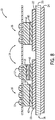
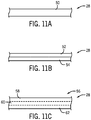
- FIGS. 11A-11C various examples diffusion barrier layers 28 are shown.
- FIG. 11C illustrates a diffusion barrier layer which is used in the surface mount package structure of the present invention.
- FIGS. 11A and 11B illustrate alternative diffusion barrier layers which are not used in the surface mount package of the present invention.
- the diffusion barrier layer 28 described with reference to FIGS. 11A-11C includes one or more layers formed of organic materials, inorganic materials, ceramic materials, and any combination thereof, with these materials typically being reaction or recombination products of reacting plasma species.
- the diffusion barrier layer 28 may be constructed as a single layer 50 having a consistent composition throughout.
- the single layer 50 may be formed of inorganic and/or ceramic materials only, with the inorganic/ceramic materials comprising any of oxides, nitrides, carbides, and borides of elements of Groups IIA, IIIA, IVA, VA, VIA, VIIA, IB, IIB, metals of Groups IIIB, IVB, VB, rare earth elements, or any combination thereof.
- the diffusion barrier layer 28 may instead be constructed as a stack of layers 52, 54 (i.e., a multi-layer construction), such as a first layer 52 and a second layer 54, although it is recognized that additional layers could be constructed.
- the first layer 52 may be formed of one or more organic materials, such as carbon, hydrogen, oxygen, and optionally other minor elements, such as sulfur, nitrogen, silicon, etc., depending on the types of reactants used therewith, with suitable reactants that result in organic compositions in the coating being straight or branched alkanes, alkenes, alkynes, alcohols, aldehydes, ethers, alkylene oxides, aromatics, etc., having up to 15 carbon atoms.
- the second layer 54 may be formed of inorganic and/or ceramic materials, with the inorganic/ceramic materials comprising any of oxides, nitrides, carbides, and borides of elements of Groups IIA, IIIA, IVA, VA, VIA, VIIA, IB, IIB, metals of Groups IIIB, IVB, VB, rare earth elements, or any combination thereof.
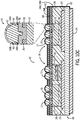
- the diffusion barrier layer 28 may be constructed as a layer 56 having a graded composition, i.e., the composition of the layer 56 varies across a thickness of the layer, such that layer 56 can be termed as having a plurality of regions 58, 60, 62.
- Suitable coating compositions of regions 58, 60, 62 across the thickness of layer 56 are organic, inorganic, or ceramic materials, such as the organic, inorganic, and ceramic materials set forth above.
- silicon carbide can be deposited onto a substrate by recombination of plasmas generated from silane (SiH 4 ) and an organic material, such as methane or xylene.
- Silicon oxycarbide can be deposited from plasmas generated from silane, methane, and oxygen or silane and propylene oxide. Silicon oxycarbide also can be deposited from plasmas generated from organosilicone precursors, such as tetraethoxysilane (TEOS), hexamethyldisiloxane (HMDSO), hexamethyldisilazane (HMDSN), or octamethylcyclotetrasiloxane (D 4 ). Silicon nitride can be deposited from plasmas generated from silane and ammonia. Aluminum oxycarbonitride can be deposited from a plasma generated from a mixture of aluminum tartrate and ammonia. Other combinations of reactants may be chosen to obtain a desired composition of layer 56. A graded composition of the layer 56 is obtained by changing the compositions of the reactants fed into the reactor chamber during the deposition of reaction products to form the layer.
- organosilicone precursors such as tetraethoxysilane (TE
- embodiments of the invention thus provide a POL packaging and interconnect structure 10 having second-level package I/O's 16 that are provided on the flex side (i.e., on top of dielectric layer 30) of the POL sub-module 14 for second-level interconnection to an external circuit and the entire non-die side DBC layer 24 is available for thermal connection.
- the POL structure 10 includes a diffusion barrier layer 28 configured to reduce the ingress of moisture and gases into the package, so as to provide enhanced reliability to moisture and gas related failure mechanisms.
- the diffusion barrier layer 28 is further configured such that it does not interfere with the solderability of the second-level I/O interconnections 16 to a PCB or other external circuit.
Description
- Embodiments of the invention relate generally to structures and methods for packaging semiconductor devices and, more particularly, to a surface-mount package structure that includes a diffusion barrier coating.
- Surface-mount technology is a method for constructing electronic circuits in which surface mount components or packages are mounted directly onto the surface of printed circuit boards (PCBs) or other similar external circuits. In the industry, surface-mount technology has replaced the through-hole technology construction method of fitting components with wire leads into holes in the circuit board.
- One common type of component that is surface-mounted is a power semiconductor device, which is a semiconductor device used as a switch or rectifier in power electronic circuits, such as switched mode power supplies, for example. Most power semiconductor devices are only used in commutation mode (i.e., they are either on or off), and are therefore optimized for this. Many power semiconductor devices are used in high voltage power applications and are designed to carry a large amount of current and support a large voltage. In use, high voltage power semiconductor devices are surface mounted to an external circuit by way of a power overlay (POL) packaging and interconnect system, with the POL package also providing a way to remove the heat generated by the device and protect the device from the external environment.
- A standard POL package manufacturing process typically begins with placement of one or more power semiconductor devices onto a dielectric layer by way of an adhesive. Metal interconnects (e.g., copper interconnects) are then electroplated onto the dielectric layer to form a direct metallic connection to the power semiconductor device(s), so as to form a POL sub-module. The metal interconnects may be in the form of a low profile (e.g., less than 200 micrometers thick), planar interconnect structure that provides for formation of an input/output (I/O) system to and from the power semiconductor device(s). The POL sub-module is then soldered to a ceramic substrate (Alumina with DBC, A1N with AMB Cu, etc.) using soldered interconnection for electrical and thermal connectivity. The gaps around the semiconductor between the POL dielectric layer and the ceramic substrate are then filled using a dielectric organic material using either capillary flow (capillary underfill), no-flow underfill or injection molding (molding compounds) to form the POL package.
- It is recognized that POL packages are susceptible to moisture, as moisture in the environment may be absorbed by the materials in the POL package. For example the module may absorb moisture within the bulk of Kapton-adhesive layers and organic dielectric material (i.e., underfill, molding compound, etc.) and at the interfaces created by these materials within the package. When soldering the POL module with absorbed moisture to a circuit board, temperatures in the range of 210-260 degrees Celsius are reached and, at these temperatures, the vapor pressure of the moisture in the POL package increases rapidly. This increase in vapor pressure can cause delamination, "pop-corning" and failure if the moisture is excessive. Additionally, in long term storage and use while exposed to moisture, excessive moisture absorption by the POL package and corrosion at dissimilar material interfaces within the package may lead to electrical and mechanical failures due to increased leakage currents and can also cause mechanical damage on interconnects due to swelling of the POL module upon reflow during board-assembly operations.
- Long term operating/storage at elevated temperatures in air (or oxygen-rich environments) or with exposure to toxic/corrosive gasses may also affect the long term life and functionality of the POL modules. With oxygen ingress at elevated temperatures, various interfaces can degrade and the mechanical/electrical/thermal performance of the module may be severely affected. As an example, the adhesion between POL metal (Cu) and Kapton is strongly affected by exposure to oxygen at elevated temperatures, with degradation of adhesion strength being seen within 1000 hrs of storage at temperatures between 200C - 250C. The inclusion of a robust diffusion barrier can slow down the ingress of oxygen (or other degrading gases) and increase the long-term life of the modules.
-
US 6306680 describes packaging of power semiconductor devices in both single chip and multiple chip packages, with enhanced electrical and thermal characteristics.US 6306680 discloses the preamble of claims 1 and 11 respectively of the present application.US 6154366 describes a chip-on-flex packaging technology which includes at least one moisture barrier layer to prevent metal corrosion and delamination of flex component layers.US 5250843 describes an improved multichip integrated circuit module including a packaging method for electronic integrated circuit chips on a substrate and having a polymer encapsulant overlying the chips. A hermetically sealed module is disclosed.US 2007/138651 describes semiconductor device packages including a direct bonded copper substrate (DBC) and processes for their manufacture. - Therefore, it would be desirable to provide a surface-mount package having a diffusion barrier that reduces the ingress of moisture and gases into the package, so as to provide enhanced reliability to moisture-related and gas-related failure mechanisms. It would further be desirable for such a diffusion barrier to be introduced during various stages of manufacture of the surface-mount package.
- The invention provides a surface-mount package in accordance with claim 1. The package includes a diffusion barrier coating configured to reduce the ingress of moisture and gases from a surrounding environment into the surface-mount structure.
- The present invention further provides a method of manufacturing a surface-mount package as defined in claim 11. Preferred embodiments are defined in the dependent claims.
- These advantages and features of the invention will be more readily understood from the following detailed description of preferred embodiments of the invention that is provided in connection with the accompanying drawings.
- The drawings illustrate embodiments of the invention.
- In the drawings:
-
FIG. 1 is a schematic cross-sectional side view of a surface mount package structure according to an embodiment of the invention. -
FIGS. 2-9 are schematic cross-sectional side views of a surface mount package structure during various stages of a manufacturing/build-up process according to an embodiment of the invention. -
FIGS. 10A-10D are schematic cross-sectional side views of a surface mount package structure having a diffusion barrier layer applied thereto according to embodiments of the invention. -
FIGS. 11A-11C are schematic cross-sectional side views of a diffusion player.FIG. 11C illustrates a diffusion barrier layer which is used in the surface mount package structure of the present invention.FIGS. 11A and 11B illustrate alternative diffusion barrier layers which are not used in the surface mount package of the invention. - Embodiments of the present invention provide for a surface-mount package having a diffusion barrier layer included thereon, as well as a method of forming such a surface-mount package. The surface-mount package is manufactured such that the diffusion barrier layer reduces the ingress of moisture and gases into the package, while still providing for attaching of the surface-mount package to an external circuit.
- Referring to
FIG. 1 , a surface-mount packaging andinterconnect structure 10 is shown according to an embodiment of the invention. In the embodiment shown inFIG. 1 , surface-mount package structure 10 is in the form of a power overlay (POL) structure, although it is recognized that other surface-mount package structures are considered to be within the scope of the invention. ThePOL structure 10 includes one or more semiconductor device(s) 12 therein that, according to various embodiments, may be in the form of a die, diode, or other power electronic device. As shown inFIG. 1 , three semiconductor device(s) 12 are provided inPOL structure 10, however, it is recognized that a greater or lesser number ofsemiconductor devices 12 could be included inPOL structure 10. The semiconductor device(s) 12 are packaged within aPOL sub-module 14 that forms a direct metallic connection to the power semiconductor device(s) 12, with the connection being in the form of a low profile, planar first-level interconnect structure, for example. - A second-level input-output (I/O)
connection 16 is provided onPOL sub-module 14 to enable surface mounting of thePOL structure 10 to an external circuit, such as a printed circuit board (PCB) (not shown). According to an exemplary embodiment, the second-level I/O connection 16 is formed of land grid array (LGA)solder bumps 17 that are configured to be attached/affixed to the PCB to electrically couple thePOL structure 10 to the PCB, although other suitable second-level solder interconnections, such as ball grid array (BGA) solder bumps, could also be used. TheLGA solder bumps 17 provide a highly reliable interconnection structure that is resistive to failure in high stress conditions. - As shown in
FIG. 1 ,POL structure 10 also includes asubstrate structure 18 to whichPOL sub-module 14 is attached. According to an exemplary embodiment, thesubstrate structure 18 is composed of a ceramic tile (e.g., alumina) 20 with a layer of direct bond copper (DBC) 22, 24 bonded to both sides thereof by a high-temperature joining process. For the joining process, different brazing and direct bond technologies may be employed based on, for example, whethertile 20 is composed of alumina or aluminum nitride and silicon nitride, etc. Thetop DBC layer 22, or "die side DBC layer," ofsubstrate structure 18 is then etched after firing, to pattern the layer as desired based on the number/arrangement ofsemiconductor devices 12. Thebottom DBC layer 24, or "non-die side DBC layer," on the backside of thesubstrate structure 18 is left fully or partially exposed to provide efficient heat transfer out from thePOL structure 10. While referred to above and here below as "DBC layers," it is recognized that aluminum can be used instead of copper as the metal layers, and thus such an embodiment is considered within the scope of the invention. Thus, use of the term "DBC layers" here below is meant to encompass asubstrate structure 18 that includes sheets of any suitablemetallic material 22, 24 (such as copper or aluminum) bonded to both sides of a ceramic tile (e.g., alumina) 20. As shown inFIG. 1 , adielectric material 26 is also provided onPOL structure 10 to fill in gaps in thePOL structure 10, so as to provide additional structural integrity toPOL structure 10. Thedielectric material 26 is generally referred to hereafter as an "underfill material," and in a preferred embodiment is an organic dielectric material that is moisture sensitive and that flows as a liquid prior to curing. However, it is recognized that thedielectric material 26 could be formed of any of a number of suitable materials, including underfills, silicones, molding compounds, encapsulates, or other suitable organic materials. - As shown in
FIG. 1 ,POL structure 10 also includes adiffusion barrier layer 28 that is applied about POL sub-module 14 ofPOL structure 10. According to embodiments of the invention,diffusion barrier layer 28 is configured to have a low permeability of moisture and gases (e.g., oxygen), so as to significantly reduce the amount of moisture and gases that are absorbed by the materials in thePOL sub-module 14,underfill material 26, and at the interfaces between materials in the sub-module, as well as prevent other contaminants from coming in contact with thePOL sub-module 14. Additionally, thebarrier layer 28 makes thePOL structure 10 more reliable to soldering operations (e.g., soldering of second-level I/O connections 16 to a PCB). Thediffusion barrier layer 28 is applied adjacent to second-level I/O connections 16 and is applied with a thickness that does not inhibit the soldering of the second-level I/O connections 16 to a PCB. Application of thediffusion barrier layer 28 toPOL structure 10 according to various embodiments of the invention is discussed in greater detail below. - Referring now to
FIGS. 2-12 , detailed views of the process steps for a technique of manufacturing thePOL structure 10 ofFIG. 1 are provided, according to an embodiment of the invention. As shown first inFIGS. 2-9 , process steps for a build-up of the POL sub-module 14 are provided. Referring toFIG. 2 , the build-up process of POL sub-module 14 begins with the placement and attachment of adielectric layer 30 or "flex layer" onto aframe structure 32. Thedielectric layer 30 is in the form of a lamination or film and is placed onframe structure 32 to provide stability during the build-up process ofPOL sub-module 14. According to embodiments of the invention, thedielectric layer 30 may be formed of one a plurality of dielectric materials, such as Kapton®, Ultem®, polytetrafluoroethylene (PTFE), Upilex®, polysulfone materials (e.g., Udel®, Radel®), or another polymer film, such as a liquid crystal polymer (LCP) or a polyimide material. - As shown in
FIG. 3 , upon securing ofdielectric layer 30 to framestructure 32, anadhesive layer 34 is deposited ontodielectric layer 30. A plurality ofvias 36 is then formed through theadhesive layer 34 anddielectric layer 30, as illustrated inFIG. 4 . According to embodiments of the invention, thevias 36 may be formed by way of a laser ablation or laser drilling process, plasma etching, photo-definition, or mechanical drilling processes. In a next step of technique, one or more semiconductor devices 12 (e.g., three semiconductor devices) are secured todielectric layer 30 by way ofadhesive layer 34, as illustrated inFIG. 5 . To secure thesemiconductor devices 12 todielectric layer 30, thesemiconductor devices 12 are placed ontoadhesive layer 34 and the adhesive 34 is then cured to secure thesemiconductor device 12 on thedielectric layer 30. According to one embodiment of the invention, and as shown inFIG. 5 ,semiconductor devices 12 may be of varying thickness/height. In order to increase a thickness/height of asemiconductor device 12, acopper shim 37 may be soldered to one or more ofsemiconductor devices 12 in order to increase its thickness/height so that the thickness/height of allsemiconductor devices 12 is equal and a back surface of thesemiconductor devices 12 is "planarized." - While the formation of
vias 36 throughadhesive layer 34 anddielectric lamination 30 is shown inFIG. 4 as being performed prior to placement ofsemiconductor devices 12 ontoadhesive layer 34, it is recognized that the placement ofsemiconductor devices 12 could occur prior to via formation. That is, depending on constraints imposed by via size,semiconductor devices 12 could first be placed onadhesive layer 34 anddielectric layer 30, with thevias 36 subsequently being formed at locations corresponding to a plurality of metalized circuits and/or connection pads (not shown) formed onsemiconductor devices 12. Furthermore, a combination of pre- and post-drilled vias could be employed as needed. - As shown in
FIGS. 6 and 7 , upon securing ofsemiconductor devices 12 on thedielectric layer 30 and the formation ofvias 36, thevias 36 are cleaned (such as through a reactive ion etching (RIE) desoot process) and subsequently metalized to form first-level interconnects 38. The first-level metal interconnects 38 are typically formed through a combination of sputtering and electroplating applications, although it is recognized that other electroless methods of metal deposition could also be used. For example, a titanium adhesion layer and copper seed layer may first be applied via a sputtering process, followed by an electroplating process that increases a thickness of the copper to a desired level. The applied metal material is then subsequently patterned into metal interconnects 38 (i.e., first level interconnects) having a desired shape and that function as vertical feed-throughs formed throughdielectric layer 30 andadhesive layer 34. The metal interconnects 38 extend out from circuits and/or connection pads (not shown) ofsemiconductor devices 12, through vias/opening 36, and out across atop surface 39 ofdielectric layer 30. - Referring now to
FIG. 8 , the technique of manufacturingPOL structure 10 continues with the attaching of the POL sub-module 14 tosubstrate structure 18. According to one embodiment of the invention,POL sub-module 14 is attached tosubstrate structure 18 by way of asolder material 40, so as to secure the POL sub-module 14 andsubstrate structure 18 together. That is, each ofsemiconductor devices 12 is soldered to the dieside DBC layer 22. A polymeric underfill, encapsulate, or molding compound 26 (e.g., epoxy or other organic filler material) is then provided onPOL structure 10 that fills in gaps in thePOL structure 10, as shown inFIG. 9 , so as to constraindielectric layer 30 and provide additional electrical insulation and structural integrity to thePOL structure 10. - Referring now to
FIGS. 10A-10D , various embodiments of a next step in the manufacturing of thePOL structure 10 is illustrated in which one or more diffusion barrier layers 28 are applied to thePOL structure 10. In each of the various alternative steps shown inFIGS. 10A-10D ,diffusion barrier layer 28 is applied to thePOL structure 10 to significantly reduce the amount of moisture and gases that are absorbed by the materials in thePOL structure 10 and at the interfaces between materials in the structure, as well as prevent other contaminants from coming in contact with thePOL sub-module 14. According to embodiments of the invention, thediffusion barrier layer 28 may include organic materials, inorganic materials, ceramic materials, and any combination thereof, with these materials typically being reaction or recombination products of reacting plasma species.. The layer formingdiffusion barrier layer 28 has a low diffusion/transmission of moisture and gas therethrough so as to collectively reduce moisture and gas ingress into thePOL structure 10. Thediffusion barrier layer 28 may be applied via any of a number of suitable processes, such as a plasma-enhanced chemical vapor deposition process, and has a desired thickness, such as a thickness in the range of one atomic layer up to 25-100 microns, such that thelayer 28 does not interfere with the solderability of the LGA/BGA solder bumps 17. Thediffusion barrier layer 28 is configured as an electrically non-conductive layer that is applied at a low temperature, such as a temperature that does not exceed approximately 250-300 degrees Celsius, for example. - Referring to
FIG. 10A , according to one embodiment of the invention, upon attaching of the POL sub-module 14 tosubstrate structure 18 and the deposition ofunderfill material 26, asolder mask layer 42 is applied over the patterned metal interconnects 38 on POL sub-module 14 to provide a protective coating for the copper shims thereof. Alternative to solder, it is recognized that thelayer 42 could be composed of some metal material other than solder, such as Ni or Ni/Au. As further shown inFIG. 10A , the second-level I/O interconnections 16 are then applied tosolder mask 42 on top of thedielectric layer 30. In one embodiment, I/O interconnections 16 are formed as LGA or BGA solder bumps 17 that are soldered tosolder mask 42 to enable surface mounting of thePOL structure 10 to an external circuit, with the solder bumps 17 providing a highly reliable second-level interconnection structure that is resistive to failure in high stress conditions. Upon application ofsolder mask 42 and second-level I/O interconnections 16,diffusion barrier layer 28 is then applied to thePOL structure 10. Thediffusion barrier layer 28 is applied oversolder mask 42 and the solder bumps 17 of second-level I/O interconnection 16, without any need for patterning the layer. Thediffusion barrier layer 28 also extends down the sides of thePOL structure 10 and to theceramic layer 20 orbackside DBC layer 24, such that theunderfill material 26 is also covered by thediffusion barrier layer 28 and thePOL structure 10 is enclosed by thebarrier layer 28. - Referring to
FIG. 10B , according to another embodiment of the invention, upon attaching of the POL sub-module 14 tosubstrate structure 18 and the deposition ofunderfill material 26,diffusion barrier layer 28 is applied to thePOL structure 10 directly onto the metal interconnects 38. Asolder mask layer 42 is then applied over thediffusion barrier layer 28 to provide a protective coating for the copper shims thereof, with thesolder mask layer 42 also being used to etch thediffusion barrier layer 28 to open at locations where the LGA solder bumps 17 are to be formed. As further shown inFIG. 10B , the second-level I/O interconnections 16 are applied tosolder mask 42, on top of thedielectric layer 30 and on top ofdiffusion barrier layer 28, with the interconnections being in the form of LGA or BGA solder bumps 17 that are soldered tosolder mask 42 to enable surface mounting of thePOL structure 10 to an external circuit. Thediffusion barrier layer 28 extends down the sides of thePOL structure 10 and to theceramic layer 20 orbackside DBC layer 24, such that theunderfill material 26 is also covered by thediffusion barrier layer 28 and thePOL structure 10 is enclosed by the barrier layer. - Referring to
FIG. 10C , according to another embodiment of the invention, multiple diffusion barrier layers 28 are applied ontoPOL structure 10 at various stages of the manufacturing process. That is, a firstdiffusion barrier layer 28A is applied to thePOL structure 10 directly onto the metal interconnects 38. Asolder mask layer 42 is then applied over thediffusion barrier layer 28A to provide a protective coating for the copper shims thereof, with the second-level I/O interconnections 16 then being applied tosolder mask 42 on top of thedielectric layer 30 and on top of the firstdiffusion barrier layer 28A, with the interconnections being in the form of LGA or BGA solder bumps 17. Upon application ofsolder mask 42 and second-level I/O interconnections 16, a seconddiffusion barrier layer 28B is then applied to the sub-module, with the seconddiffusion barrier layer 28B being applied oversolder mask 42 and the solder bumps 17 of second-level I/O interconnection 16, without any need for patterning the layer. The seconddiffusion barrier layer 28B is configured such that the layer does not interfere with the solderability of the LGA/BGA solder bumps 17. Additionally, the first and/or second diffusion barrier layers 28A, 28B extend down the sides of the POL structure and to theceramic layer 20 orbackside DBC layer 24, such that theunderfill material 26 is also covered by the diffusion barrier layer and thePOL structure 10 is enclosed by the barrier layer. - Referring to
FIG. 10D , according to another embodiment of the invention, upon attaching of the POL sub-module 14 tosubstrate structure 18 and the deposition ofunderfill material 26,diffusion barrier layer 28 is applied to thePOL structure 10 directly onto the metal interconnects 38 and is configured to act as a solder mask. In replacing the function of the traditional solder mask, a thickness ofdiffusion barrier layer 28 is increased such that the barrier layer provides adequate protection to metal interconnects 38. Upon application of thediffusion barrier layer 28, the second-level I/O interconnections 16 are formed thereover, with the interconnections being in the form of LGA or BGA solder bumps 17. - Referring now to
FIGS. 11A-11C , various examples diffusion barrier layers 28 are shown.FIG. 11C illustrates a diffusion barrier layer which is used in the surface mount package structure of the present invention.FIGS. 11A and 11B illustrate alternative diffusion barrier layers which are not used in the surface mount package of the present invention. Thediffusion barrier layer 28 described with reference toFIGS. 11A-11C includes one or more layers formed of organic materials, inorganic materials, ceramic materials, and any combination thereof, with these materials typically being reaction or recombination products of reacting plasma species. - As shown in
FIG. 11A , thediffusion barrier layer 28 may be constructed as asingle layer 50 having a consistent composition throughout. According to one example, thesingle layer 50 may be formed of inorganic and/or ceramic materials only, with the inorganic/ceramic materials comprising any of oxides, nitrides, carbides, and borides of elements of Groups IIA, IIIA, IVA, VA, VIA, VIIA, IB, IIB, metals of Groups IIIB, IVB, VB, rare earth elements, or any combination thereof. - As shown in
FIG. 11B , thediffusion barrier layer 28 may instead be constructed as a stack oflayers 52, 54 (i.e., a multi-layer construction), such as afirst layer 52 and asecond layer 54, although it is recognized that additional layers could be constructed. According to one example, thefirst layer 52 may be formed of one or more organic materials, such as carbon, hydrogen, oxygen, and optionally other minor elements, such as sulfur, nitrogen, silicon, etc., depending on the types of reactants used therewith, with suitable reactants that result in organic compositions in the coating being straight or branched alkanes, alkenes, alkynes, alcohols, aldehydes, ethers, alkylene oxides, aromatics, etc., having up to 15 carbon atoms. Thesecond layer 54 may be formed of inorganic and/or ceramic materials, with the inorganic/ceramic materials comprising any of oxides, nitrides, carbides, and borides of elements of Groups IIA, IIIA, IVA, VA, VIA, VIIA, IB, IIB, metals of Groups IIIB, IVB, VB, rare earth elements, or any combination thereof. - As shown in
FIG. 11C , according to yet another example, thediffusion barrier layer 28 may be constructed as alayer 56 having a graded composition, i.e., the composition of thelayer 56 varies across a thickness of the layer, such thatlayer 56 can be termed as having a plurality ofregions regions layer 56 are organic, inorganic, or ceramic materials, such as the organic, inorganic, and ceramic materials set forth above. For example, silicon carbide can be deposited onto a substrate by recombination of plasmas generated from silane (SiH4) and an organic material, such as methane or xylene. Silicon oxycarbide can be deposited from plasmas generated from silane, methane, and oxygen or silane and propylene oxide. Silicon oxycarbide also can be deposited from plasmas generated from organosilicone precursors, such as tetraethoxysilane (TEOS), hexamethyldisiloxane (HMDSO), hexamethyldisilazane (HMDSN), or octamethylcyclotetrasiloxane (D4). Silicon nitride can be deposited from plasmas generated from silane and ammonia. Aluminum oxycarbonitride can be deposited from a plasma generated from a mixture of aluminum tartrate and ammonia. Other combinations of reactants may be chosen to obtain a desired composition oflayer 56. A graded composition of thelayer 56 is obtained by changing the compositions of the reactants fed into the reactor chamber during the deposition of reaction products to form the layer. - Beneficially, embodiments of the invention thus provide a POL packaging and
interconnect structure 10 having second-level package I/O's 16 that are provided on the flex side (i.e., on top of dielectric layer 30) of the POL sub-module 14 for second-level interconnection to an external circuit and the entire non-dieside DBC layer 24 is available for thermal connection. ThePOL structure 10 includes adiffusion barrier layer 28 configured to reduce the ingress of moisture and gases into the package, so as to provide enhanced reliability to moisture and gas related failure mechanisms. Thediffusion barrier layer 28 is further configured such that it does not interfere with the solderability of the second-level I/O interconnections 16 to a PCB or other external circuit. - The invention is not to be seen as limited by the foregoing embodiments, but is only limited by the scope of the appended claims.
Claims (15)
- A surface-mount package structure (10) comprising:
a sub-module (14), the sub-module comprising:a dielectric layer (30);an adhesive layer (34) directly attached to the dielectric layer (30);at least one semiconductor device (12) adhered to the dielectric layer (30) via the adhesive layer (34), with each of the at least one semiconductor device (12) including a substrate (18) composed of a semiconductor material;a first level metal interconnect structure (38) electrically coupled to the at least one semiconductor device (12), the metal interconnect structure (38) extending through vias (36) formed through the dielectric layer (30) so as to be connected to the at least one semiconductor device (12); anda second level input/output, I/O, connection (16) electrically coupled to the first level metal interconnect structure (38) and formed on the dielectric layer (30) on a side opposite the at least one semiconductor device (12), the second level I/O connection (16) configured to connect the sub-module (14) to an external circuit;the surface-mount package structure further comprising:a multi-layer substrate structure (18) that includes a center substrate layer (20) and first and second metallic layers (22, 24) on opposing sides of the center substrate layer (29), such that the first and second metallic layers form first surface and a second surface, wherein the side of the at least one semiconductor device (12) of the sub-module (14) which is opposite to the side adhered to the dielectric layer (30) is attached to the first surface of the multi-layer substrate (18); anda dielectric material (26) positioned between the dielectric layer (30) and the first surface of the multi-layer substrate structure (18) and at least partially about the at least one semiconductor device (12) of the sub-module (14); characterized in that the surface-mount package structure further comprises:a diffusion barrier layer (28) applied over the sub-module (14), the diffusion barrier layer (40) extending on the dielectric layer (30) from the second level I/O connection (16) iown to the multi-layer substrate structure (18), such that the dielectric material (26) is also covered by the diffusion barrier layer (28), the diffusion barrier layer configured to reduce the ingress of moisture and gases from a surrounding environment into the surface-mount package structure (10), wherein the diffusion barrier layer (28) comprises a layer (56) having a graded composition that varies across a thickness of the layer. - The surface-mount ; package structure of claim 1, wherein the diffusion barrier (28) layer comprises organic materials, inorganic materials, ceramic materials, and any combination thereof.
- The surface-mount ; package structure of claim 2, wherein the inorganic material or ceramic comprises oxides, nitrides, carbides, and borides of elements of Groups IIA, IIIA, IVA, VA, VIA, VIIA, IB, IIB, metals of Groups IIIB, IVB, VB, rare earth elements, and any combination thereof.
- The surface-mount package structure of any of claims 1 to 3, wherein the composition of the graded layer (56) varies across the thickness of the graded layer (56) between organic and inorganic materials.
- The surface-mount ; package structure of any of claims 1 to 4, further comprising a solder mask (42) applied over the first level metal interconnect structure (38); and wherein the second level I/O connection (16) comprises one of land grid array, LGA, solder bumps (17) and ball grid array, BGA, solder bumps configured to pass through the solder mask (42) at desired locations so as to be electrically coupled to the first level metal interconnect structure (16).
- The surface-mount ; package structure of claim 5, wherein the diffusion barrier layer (28) is applied between the first level metal interconnect structure (38) and the solder mask.
- The surface-mount ; package structure of claim 5, wherein the diffusion barrier layer (28) is applied over the solder mask (42) and over or around the solder bumps (17) of the second level I/O connection (16).
- The surface-mount ; package structure of any of claims 1 to 4, wherein the diffusion barrier layer (28) is applied over the first level metal interconnect structure (16) and is further configured to function as a solder mask (42).
- The surface-mount ; package structure of any preceding claim, wherein the diffusion barrier layer (28) has a thickness of between one atomic layer and 100 micrometers
- The surface-mount ; package structure of any preceding claim, wherein the multi-layer substrate (18) structure comprises:a ceramic insulating layer as said center substrate layer (20);wherein the first and second metallic layers (22,24) comprise first and second direct bond copper (DBC) layers.
- A method of manufacturing a surface-mount package structure according to claim 1, comprising:
constructing a sub-module (14) including at least one semiconductor device (12), wherein constructing the sub-module (14) comprises:attaching the at least one semiconductor device (12) to a dielectric layer (30) using an adhesive layer (34) directly attached to the dielectric layer (30);forming a first level metal interconnect structure (38) over the dielectric layer (30), the first level metal interconnect structure (38) extending through vias (36) in the dielectric layer (30) to electrically connect to the at least one semiconductor device (12); andforming a second level input/output (I/O) connection (16) on the dielectric layer (30) on a side opposite the at least one semiconductor device (12), the second level I/O connection (16) electrically coupled to the first level metal interconnect structure (38) and configured to connect the sub-module (14) to an external circuit;forming a multi-layer substrate structure (18) that includes a center substrate layer (20) and first and second metallic layers (22,24) on opposing sides of the center substrate layer (20), such that the first and second metallic layers (22,24) form a first surface and a second surface, respectively, of the substrate structure (18);attaching the at least one semiconductor device (12) of the sub-module (14) with its side opposite the side facing the dielectric layer (30) to the first surface of the substrate structure (18);providing a dielectric material (26) between the dielectric layer (30) and the first surface of the substrate structure (18), the dielectric material (26) at least partially encapsulating the at least one semiconductor device (12) of the sub-module (14); characterized in that the method further comprises:applying a diffusion barrier layer (28) applied over the sub-module (14), the diffusion barrier layer (40) extending on the dielectric layer (30) from the second level I/O connection (16) down to the multi-layer substrate structure (18), such that the dielectric material (26) is also covered by the diffusion barrier layer (28), the diffusion barrier layer (28) configured to reduce the ingress of moisture and gases from a surrounding environment into the surface-mount package structure (10);wherein the diffusion barrier layer (28) is applied as a layer (56) having a graded composition that varies across a thickness of the layer. - The method of claim 11, further comprising applying a solder mask (42) over the first level metal interconnect structure (38), with the second level I/O connection (16) extending through the solder mask (42) at pre-determined locations.
- The method of claim 12, wherein applying the diffusion barrier layer (28) comprises applying the diffusion barrier layer (28) between the first level metal interconnect (38) structure and the solder mask (42).
- The method of claim 12, wherein applying the diffusion barrier layer (28) comprises applying the diffusion barrier layer (28) over the solder mask (42) and over or around the second level I/O connection. (16)
- The method of claim 12, wherein applying the diffusion barrier layer (28) comprises applying an organic material, an inorganic material, a ceramic material, or any combination thereof.
Applications Claiming Priority (1)
| Application Number | Priority Date | Filing Date | Title |
|---|---|---|---|
| US13/561,868 US9299630B2 (en) | 2012-07-30 | 2012-07-30 | Diffusion barrier for surface mount modules |
Publications (3)
| Publication Number | Publication Date |
|---|---|
| EP2693470A2 EP2693470A2 (en) | 2014-02-05 |
| EP2693470A3 EP2693470A3 (en) | 2015-07-22 |
| EP2693470B1 true EP2693470B1 (en) | 2020-10-28 |
Family
ID=48803437
Family Applications (1)
| Application Number | Title | Priority Date | Filing Date |
|---|---|---|---|
| EP13177219.6A Active EP2693470B1 (en) | 2012-07-30 | 2013-07-19 | Surface mount module with diffusion barrier and method of making the same |
Country Status (7)
| Country | Link |
|---|---|
| US (1) | US9299630B2 (en) |
| EP (1) | EP2693470B1 (en) |
| JP (1) | JP6266251B2 (en) |
| KR (1) | KR102089926B1 (en) |
| CN (1) | CN103579136B (en) |
| SG (2) | SG10201508888UA (en) |
| TW (1) | TWI588957B (en) |
Families Citing this family (21)
| Publication number | Priority date | Publication date | Assignee | Title |
|---|---|---|---|---|
| US10269688B2 (en) | 2013-03-14 | 2019-04-23 | General Electric Company | Power overlay structure and method of making same |
| US8987876B2 (en) | 2013-03-14 | 2015-03-24 | General Electric Company | Power overlay structure and method of making same |
| KR102117477B1 (en) * | 2015-04-23 | 2020-06-01 | 삼성전기주식회사 | Semiconductor package and manufacturing method thereof |
| US9711713B1 (en) * | 2016-01-15 | 2017-07-18 | Taiwan Semiconductor Manufacturing Company Ltd. | Semiconductor structure, electrode structure and method of forming the same |
| US10453786B2 (en) | 2016-01-19 | 2019-10-22 | General Electric Company | Power electronics package and method of manufacturing thereof |
| CN205807211U (en) * | 2016-06-20 | 2016-12-14 | 冯霞 | Light-emitting device for container |
| FR3061404B1 (en) * | 2016-12-27 | 2022-09-23 | Packaging Sip | METHOD FOR THE COLLECTIVE MANUFACTURING OF HERMETIC ELECTRONIC MODULES |
| US10541209B2 (en) | 2017-08-03 | 2020-01-21 | General Electric Company | Electronics package including integrated electromagnetic interference shield and method of manufacturing thereof |
| US10804115B2 (en) | 2017-08-03 | 2020-10-13 | General Electric Company | Electronics package with integrated interconnect structure and method of manufacturing thereof |
| US10541153B2 (en) | 2017-08-03 | 2020-01-21 | General Electric Company | Electronics package with integrated interconnect structure and method of manufacturing thereof |
| US10332832B2 (en) | 2017-08-07 | 2019-06-25 | General Electric Company | Method of manufacturing an electronics package using device-last or device-almost last placement |
| US10685935B2 (en) | 2017-11-15 | 2020-06-16 | Taiwan Semiconductor Manufacturing Company, Ltd. | Forming metal bonds with recesses |
| CN108044259B (en) * | 2017-12-01 | 2020-04-03 | 温州宏丰电工合金股份有限公司 | Preparation method of flow resisting agent for stainless steel vacuum brazing |
| CN108098093B (en) * | 2017-12-01 | 2020-04-03 | 温州宏丰电工合金股份有限公司 | Flow resisting agent for stainless steel vacuum brazing |
| EP3518278A1 (en) * | 2018-01-30 | 2019-07-31 | Infineon Technologies AG | Power semiconductor module and method for producing the same |
| KR20200138262A (en) * | 2018-03-26 | 2020-12-09 | 미쓰비시 마테리알 가부시키가이샤 | Method for manufacturing a bonded body for an insulated circuit board and a bonded body for an insulated circuit board |
| US11538769B2 (en) | 2018-12-14 | 2022-12-27 | General Electric Company | High voltage semiconductor devices having improved electric field suppression |
| US10892237B2 (en) * | 2018-12-14 | 2021-01-12 | General Electric Company | Methods of fabricating high voltage semiconductor devices having improved electric field suppression |
| US11398445B2 (en) | 2020-05-29 | 2022-07-26 | General Electric Company | Mechanical punched via formation in electronics package and electronics package formed thereby |
| WO2023190107A1 (en) * | 2022-03-31 | 2023-10-05 | 株式会社Flosfia | Semiconductor device |
| WO2023190106A1 (en) * | 2022-03-31 | 2023-10-05 | 株式会社Flosfia | Semiconductor device |
Citations (1)
| Publication number | Priority date | Publication date | Assignee | Title |
|---|---|---|---|---|
| US20040046497A1 (en) * | 2002-09-11 | 2004-03-11 | General Electric Company | Diffusion barrier coatings having graded compositions and devices incorporating the same |
Family Cites Families (22)
| Publication number | Priority date | Publication date | Assignee | Title |
|---|---|---|---|---|
| US5250843A (en) | 1991-03-27 | 1993-10-05 | Integrated System Assemblies Corp. | Multichip integrated circuit modules |
| TW272311B (en) * | 1994-01-12 | 1996-03-11 | At & T Corp | |
| US7653215B2 (en) * | 1997-04-02 | 2010-01-26 | Gentex Corporation | System for controlling exterior vehicle lights |
| US6306680B1 (en) | 1999-02-22 | 2001-10-23 | General Electric Company | Power overlay chip scale packages for discrete power devices |
| US6154366A (en) | 1999-11-23 | 2000-11-28 | Intel Corporation | Structures and processes for fabricating moisture resistant chip-on-flex packages |
| US6551148B1 (en) * | 2001-10-19 | 2003-04-22 | Hewlett-Packard Development Company, L.P. | Electrical connector with minimized non-target contact |
| US7169345B2 (en) * | 2003-08-27 | 2007-01-30 | Texas Instruments Incorporated | Method for integrated circuit packaging |
| WO2005051525A1 (en) | 2003-11-25 | 2005-06-09 | Polyvalor, Limited Partnership | Permeation barrier coating or layer with modulated properties and methods of making the same |
| US7262444B2 (en) * | 2005-08-17 | 2007-08-28 | General Electric Company | Power semiconductor packaging method and structure |
| US8018056B2 (en) * | 2005-12-21 | 2011-09-13 | International Rectifier Corporation | Package for high power density devices |
| TWI350793B (en) | 2006-03-08 | 2011-10-21 | E Ink Corp | Methods for production of electro-optic displays |
| US20070295387A1 (en) | 2006-05-05 | 2007-12-27 | Nanosolar, Inc. | Solar assembly with a multi-ply barrier layer and individually encapsulated solar cells or solar cell strings |
| US7688497B2 (en) | 2007-01-22 | 2010-03-30 | E Ink Corporation | Multi-layer sheet for use in electro-optic displays |
| US9953910B2 (en) * | 2007-06-21 | 2018-04-24 | General Electric Company | Demountable interconnect structure |
| JP5241177B2 (en) * | 2007-09-05 | 2013-07-17 | 株式会社オクテック | Semiconductor device and manufacturing method of semiconductor device |
| US20100308468A1 (en) * | 2008-03-14 | 2010-12-09 | Noriyuki Yoshikawa | Semiconductor device and semiconductor device fabrication method |
| DE102008028757B4 (en) * | 2008-06-17 | 2017-03-16 | Epcos Ag | Method for producing a semiconductor chip arrangement |
| US8358000B2 (en) * | 2009-03-13 | 2013-01-22 | General Electric Company | Double side cooled power module with power overlay |
| WO2011103341A1 (en) | 2010-02-18 | 2011-08-25 | Alliance For Sustainable Energy, Llc | Moisture barrier |
| JP2010212698A (en) * | 2010-04-01 | 2010-09-24 | Sony Chemical & Information Device Corp | Connection structure and its manufacturing method |
| US8531027B2 (en) * | 2010-04-30 | 2013-09-10 | General Electric Company | Press-pack module with power overlay interconnection |
| US8114712B1 (en) * | 2010-12-22 | 2012-02-14 | General Electric Company | Method for fabricating a semiconductor device package |
-
2012
- 2012-07-30 US US13/561,868 patent/US9299630B2/en active Active
-
2013
- 2013-07-15 TW TW102125294A patent/TWI588957B/en active
- 2013-07-19 EP EP13177219.6A patent/EP2693470B1/en active Active
- 2013-07-25 SG SG10201508888UA patent/SG10201508888UA/en unknown
- 2013-07-25 SG SG2013056924A patent/SG196754A1/en unknown
- 2013-07-26 JP JP2013155115A patent/JP6266251B2/en active Active
- 2013-07-29 KR KR1020130089684A patent/KR102089926B1/en active IP Right Grant
- 2013-07-30 CN CN201310324406.0A patent/CN103579136B/en active Active
Patent Citations (1)
| Publication number | Priority date | Publication date | Assignee | Title |
|---|---|---|---|---|
| US20040046497A1 (en) * | 2002-09-11 | 2004-03-11 | General Electric Company | Diffusion barrier coatings having graded compositions and devices incorporating the same |
Also Published As
| Publication number | Publication date |
|---|---|
| EP2693470A3 (en) | 2015-07-22 |
| SG10201508888UA (en) | 2015-11-27 |
| KR20140016192A (en) | 2014-02-07 |
| SG196754A1 (en) | 2014-02-13 |
| CN103579136B (en) | 2018-03-06 |
| JP6266251B2 (en) | 2018-01-24 |
| JP2014027277A (en) | 2014-02-06 |
| TWI588957B (en) | 2017-06-21 |
| CN103579136A (en) | 2014-02-12 |
| KR102089926B1 (en) | 2020-04-14 |
| US9299630B2 (en) | 2016-03-29 |
| US20140029210A1 (en) | 2014-01-30 |
| TW201409635A (en) | 2014-03-01 |
| EP2693470A2 (en) | 2014-02-05 |
Similar Documents
| Publication | Publication Date | Title |
|---|---|---|
| EP2693470B1 (en) | Surface mount module with diffusion barrier and method of making the same | |
| US9184124B2 (en) | Reliable surface mount integrated power module | |
| US11177204B2 (en) | Power electronics package and method of manufacturing thereof | |
| US10186477B2 (en) | Power overlay structure and method of making same | |
| US8653635B2 (en) | Power overlay structure with leadframe connections | |
| KR100851072B1 (en) | Electronic package and manufacturing method thereof | |
| JP2018120902A (en) | Power electronics package and method of manufacturing the same | |
| CN108428689B (en) | Power electronic device assembly and method of manufacturing the same | |
| TWI697077B (en) | Power electronics package and method of manufacturing thereof | |
| KR100836657B1 (en) | Electronic package and manufacturing method thereof | |
| KR20180092379A (en) | Power electronics package and method of manufacturing thereof |
Legal Events
| Date | Code | Title | Description |
|---|---|---|---|
| AK | Designated contracting states |
Kind code of ref document: A2 Designated state(s): AL AT BE BG CH CY CZ DE DK EE ES FI FR GB GR HR HU IE IS IT LI LT LU LV MC MK MT NL NO PL PT RO RS SE SI SK SM TR |
|
| AX | Request for extension of the european patent |
Extension state: BA ME |
|
| PUAI | Public reference made under article 153(3) epc to a published international application that has entered the european phase |
Free format text: ORIGINAL CODE: 0009012 |
|
| PUAL | Search report despatched |
Free format text: ORIGINAL CODE: 0009013 |
|
| AK | Designated contracting states |
Kind code of ref document: A3 Designated state(s): AL AT BE BG CH CY CZ DE DK EE ES FI FR GB GR HR HU IE IS IT LI LT LU LV MC MK MT NL NO PL PT RO RS SE SI SK SM TR |
|
| AX | Request for extension of the european patent |
Extension state: BA ME |
|
| RIC1 | Information provided on ipc code assigned before grant |
Ipc: H01L 23/00 20060101ALI20150618BHEP Ipc: H01L 23/498 20060101ALI20150618BHEP Ipc: H01L 23/538 20060101ALI20150618BHEP Ipc: H01L 23/31 20060101AFI20150618BHEP Ipc: H01L 23/532 20060101ALI20150618BHEP Ipc: H01L 21/56 20060101ALN20150618BHEP Ipc: H01L 23/373 20060101ALI20150618BHEP Ipc: H01L 21/48 20060101ALI20150618BHEP |
|
| 17P | Request for examination filed |
Effective date: 20160122 |
|
| RBV | Designated contracting states (corrected) |
Designated state(s): AL AT BE BG CH CY CZ DE DK EE ES FI FR GB GR HR HU IE IS IT LI LT LU LV MC MK MT NL NO PL PT RO RS SE SI SK SM TR |
|
| STAA | Information on the status of an ep patent application or granted ep patent |
Free format text: STATUS: EXAMINATION IS IN PROGRESS |
|
| 17Q | First examination report despatched |
Effective date: 20180425 |
|
| GRAP | Despatch of communication of intention to grant a patent |
Free format text: ORIGINAL CODE: EPIDOSNIGR1 |
|
| RIC1 | Information provided on ipc code assigned before grant |
Ipc: H01L 23/532 20060101ALI20200608BHEP Ipc: H01L 21/48 20060101ALI20200608BHEP Ipc: H01L 23/00 20060101ALI20200608BHEP Ipc: H01L 23/31 20060101AFI20200608BHEP Ipc: H01L 23/498 20060101ALI20200608BHEP Ipc: H01L 21/56 20060101ALN20200608BHEP Ipc: H01L 23/538 20060101ALI20200608BHEP Ipc: H01L 23/373 20060101ALI20200608BHEP |
|
| STAA | Information on the status of an ep patent application or granted ep patent |
Free format text: STATUS: GRANT OF PATENT IS INTENDED |
|
| RIC1 | Information provided on ipc code assigned before grant |
Ipc: H01L 23/538 20060101ALI20200616BHEP Ipc: H01L 23/532 20060101ALI20200616BHEP Ipc: H01L 23/373 20060101ALI20200616BHEP Ipc: H01L 21/56 20060101ALN20200616BHEP Ipc: H01L 21/48 20060101ALI20200616BHEP Ipc: H01L 23/00 20060101ALI20200616BHEP Ipc: H01L 23/31 20060101AFI20200616BHEP Ipc: H01L 23/498 20060101ALI20200616BHEP |
|
| INTG | Intention to grant announced |
Effective date: 20200716 |
|
| RIC1 | Information provided on ipc code assigned before grant |
Ipc: H01L 23/538 20060101ALI20200706BHEP Ipc: H01L 23/373 20060101ALI20200706BHEP Ipc: H01L 23/00 20060101ALI20200706BHEP Ipc: H01L 21/48 20060101ALI20200706BHEP Ipc: H01L 23/31 20060101AFI20200706BHEP Ipc: H01L 23/498 20060101ALI20200706BHEP Ipc: H01L 23/532 20060101ALI20200706BHEP Ipc: H01L 21/56 20060101ALN20200706BHEP |
|
| RIN1 | Information on inventor provided before grant (corrected) |
Inventor name: ZHAO, RI-AN Inventor name: MCCONNELEE, PAUL ALAN Inventor name: CHAUHAN, SHAKTI SINGH Inventor name: GOWDA, ARUN VIRUPAKSHA |
|
| GRAS | Grant fee paid |
Free format text: ORIGINAL CODE: EPIDOSNIGR3 |
|
| GRAA | (expected) grant |
Free format text: ORIGINAL CODE: 0009210 |
|
| STAA | Information on the status of an ep patent application or granted ep patent |
Free format text: STATUS: THE PATENT HAS BEEN GRANTED |
|
| AK | Designated contracting states |
Kind code of ref document: B1 Designated state(s): AL AT BE BG CH CY CZ DE DK EE ES FI FR GB GR HR HU IE IS IT LI LT LU LV MC MK MT NL NO PL PT RO RS SE SI SK SM TR |
|
| REG | Reference to a national code |
Ref country code: GB Ref legal event code: FG4D |
|
| REG | Reference to a national code |
Ref country code: CH Ref legal event code: EP |
|
| REG | Reference to a national code |
Ref country code: DE Ref legal event code: R096 Ref document number: 602013073566 Country of ref document: DE |
|
| REG | Reference to a national code |
Ref country code: AT Ref legal event code: REF Ref document number: 1329078 Country of ref document: AT Kind code of ref document: T Effective date: 20201115 |
|
| REG | Reference to a national code |
Ref country code: IE Ref legal event code: FG4D |
|
| REG | Reference to a national code |
Ref country code: AT Ref legal event code: MK05 Ref document number: 1329078 Country of ref document: AT Kind code of ref document: T Effective date: 20201028 |
|
| REG | Reference to a national code |
Ref country code: NL Ref legal event code: MP Effective date: 20201028 |
|
| PG25 | Lapsed in a contracting state [announced via postgrant information from national office to epo] |
Ref country code: GR Free format text: LAPSE BECAUSE OF FAILURE TO SUBMIT A TRANSLATION OF THE DESCRIPTION OR TO PAY THE FEE WITHIN THE PRESCRIBED TIME-LIMIT Effective date: 20210129 Ref country code: FI Free format text: LAPSE BECAUSE OF FAILURE TO SUBMIT A TRANSLATION OF THE DESCRIPTION OR TO PAY THE FEE WITHIN THE PRESCRIBED TIME-LIMIT Effective date: 20201028 Ref country code: RS Free format text: LAPSE BECAUSE OF FAILURE TO SUBMIT A TRANSLATION OF THE DESCRIPTION OR TO PAY THE FEE WITHIN THE PRESCRIBED TIME-LIMIT Effective date: 20201028 Ref country code: NO Free format text: LAPSE BECAUSE OF FAILURE TO SUBMIT A TRANSLATION OF THE DESCRIPTION OR TO PAY THE FEE WITHIN THE PRESCRIBED TIME-LIMIT Effective date: 20210128 Ref country code: PT Free format text: LAPSE BECAUSE OF FAILURE TO SUBMIT A TRANSLATION OF THE DESCRIPTION OR TO PAY THE FEE WITHIN THE PRESCRIBED TIME-LIMIT Effective date: 20210301 Ref country code: NL Free format text: LAPSE BECAUSE OF FAILURE TO SUBMIT A TRANSLATION OF THE DESCRIPTION OR TO PAY THE FEE WITHIN THE PRESCRIBED TIME-LIMIT Effective date: 20201028 |
|
| REG | Reference to a national code |
Ref country code: LT Ref legal event code: MG4D |
|
| PG25 | Lapsed in a contracting state [announced via postgrant information from national office to epo] |
Ref country code: BG Free format text: LAPSE BECAUSE OF FAILURE TO SUBMIT A TRANSLATION OF THE DESCRIPTION OR TO PAY THE FEE WITHIN THE PRESCRIBED TIME-LIMIT Effective date: 20210128 Ref country code: AT Free format text: LAPSE BECAUSE OF FAILURE TO SUBMIT A TRANSLATION OF THE DESCRIPTION OR TO PAY THE FEE WITHIN THE PRESCRIBED TIME-LIMIT Effective date: 20201028 Ref country code: ES Free format text: LAPSE BECAUSE OF FAILURE TO SUBMIT A TRANSLATION OF THE DESCRIPTION OR TO PAY THE FEE WITHIN THE PRESCRIBED TIME-LIMIT Effective date: 20201028 Ref country code: SE Free format text: LAPSE BECAUSE OF FAILURE TO SUBMIT A TRANSLATION OF THE DESCRIPTION OR TO PAY THE FEE WITHIN THE PRESCRIBED TIME-LIMIT Effective date: 20201028 Ref country code: PL Free format text: LAPSE BECAUSE OF FAILURE TO SUBMIT A TRANSLATION OF THE DESCRIPTION OR TO PAY THE FEE WITHIN THE PRESCRIBED TIME-LIMIT Effective date: 20201028 Ref country code: LV Free format text: LAPSE BECAUSE OF FAILURE TO SUBMIT A TRANSLATION OF THE DESCRIPTION OR TO PAY THE FEE WITHIN THE PRESCRIBED TIME-LIMIT Effective date: 20201028 Ref country code: IS Free format text: LAPSE BECAUSE OF FAILURE TO SUBMIT A TRANSLATION OF THE DESCRIPTION OR TO PAY THE FEE WITHIN THE PRESCRIBED TIME-LIMIT Effective date: 20210228 |
|
| PG25 | Lapsed in a contracting state [announced via postgrant information from national office to epo] |
Ref country code: HR Free format text: LAPSE BECAUSE OF FAILURE TO SUBMIT A TRANSLATION OF THE DESCRIPTION OR TO PAY THE FEE WITHIN THE PRESCRIBED TIME-LIMIT Effective date: 20201028 |
|
| REG | Reference to a national code |
Ref country code: DE Ref legal event code: R097 Ref document number: 602013073566 Country of ref document: DE |
|
| PG25 | Lapsed in a contracting state [announced via postgrant information from national office to epo] |
Ref country code: SK Free format text: LAPSE BECAUSE OF FAILURE TO SUBMIT A TRANSLATION OF THE DESCRIPTION OR TO PAY THE FEE WITHIN THE PRESCRIBED TIME-LIMIT Effective date: 20201028 Ref country code: RO Free format text: LAPSE BECAUSE OF FAILURE TO SUBMIT A TRANSLATION OF THE DESCRIPTION OR TO PAY THE FEE WITHIN THE PRESCRIBED TIME-LIMIT Effective date: 20201028 Ref country code: LT Free format text: LAPSE BECAUSE OF FAILURE TO SUBMIT A TRANSLATION OF THE DESCRIPTION OR TO PAY THE FEE WITHIN THE PRESCRIBED TIME-LIMIT Effective date: 20201028 Ref country code: EE Free format text: LAPSE BECAUSE OF FAILURE TO SUBMIT A TRANSLATION OF THE DESCRIPTION OR TO PAY THE FEE WITHIN THE PRESCRIBED TIME-LIMIT Effective date: 20201028 Ref country code: CZ Free format text: LAPSE BECAUSE OF FAILURE TO SUBMIT A TRANSLATION OF THE DESCRIPTION OR TO PAY THE FEE WITHIN THE PRESCRIBED TIME-LIMIT Effective date: 20201028 Ref country code: SM Free format text: LAPSE BECAUSE OF FAILURE TO SUBMIT A TRANSLATION OF THE DESCRIPTION OR TO PAY THE FEE WITHIN THE PRESCRIBED TIME-LIMIT Effective date: 20201028 |
|
| PG25 | Lapsed in a contracting state [announced via postgrant information from national office to epo] |
Ref country code: DK Free format text: LAPSE BECAUSE OF FAILURE TO SUBMIT A TRANSLATION OF THE DESCRIPTION OR TO PAY THE FEE WITHIN THE PRESCRIBED TIME-LIMIT Effective date: 20201028 |
|
| PLBE | No opposition filed within time limit |
Free format text: ORIGINAL CODE: 0009261 |
|
| STAA | Information on the status of an ep patent application or granted ep patent |
Free format text: STATUS: NO OPPOSITION FILED WITHIN TIME LIMIT |
|
| 26N | No opposition filed |
Effective date: 20210729 |
|
| PG25 | Lapsed in a contracting state [announced via postgrant information from national office to epo] |
Ref country code: IT Free format text: LAPSE BECAUSE OF FAILURE TO SUBMIT A TRANSLATION OF THE DESCRIPTION OR TO PAY THE FEE WITHIN THE PRESCRIBED TIME-LIMIT Effective date: 20201028 Ref country code: AL Free format text: LAPSE BECAUSE OF FAILURE TO SUBMIT A TRANSLATION OF THE DESCRIPTION OR TO PAY THE FEE WITHIN THE PRESCRIBED TIME-LIMIT Effective date: 20201028 |
|
| PG25 | Lapsed in a contracting state [announced via postgrant information from national office to epo] |
Ref country code: SI Free format text: LAPSE BECAUSE OF FAILURE TO SUBMIT A TRANSLATION OF THE DESCRIPTION OR TO PAY THE FEE WITHIN THE PRESCRIBED TIME-LIMIT Effective date: 20201028 |
|
| REG | Reference to a national code |
Ref country code: CH Ref legal event code: PL |
|
| PG25 | Lapsed in a contracting state [announced via postgrant information from national office to epo] |
Ref country code: MC Free format text: LAPSE BECAUSE OF FAILURE TO SUBMIT A TRANSLATION OF THE DESCRIPTION OR TO PAY THE FEE WITHIN THE PRESCRIBED TIME-LIMIT Effective date: 20201028 |
|
| REG | Reference to a national code |
Ref country code: BE Ref legal event code: MM Effective date: 20210731 |
|
| PG25 | Lapsed in a contracting state [announced via postgrant information from national office to epo] |
Ref country code: LI Free format text: LAPSE BECAUSE OF NON-PAYMENT OF DUE FEES Effective date: 20210731 Ref country code: CH Free format text: LAPSE BECAUSE OF NON-PAYMENT OF DUE FEES Effective date: 20210731 |
|
| PG25 | Lapsed in a contracting state [announced via postgrant information from national office to epo] |
Ref country code: IS Free format text: LAPSE BECAUSE OF FAILURE TO SUBMIT A TRANSLATION OF THE DESCRIPTION OR TO PAY THE FEE WITHIN THE PRESCRIBED TIME-LIMIT Effective date: 20210228 Ref country code: LU Free format text: LAPSE BECAUSE OF NON-PAYMENT OF DUE FEES Effective date: 20210719 |
|
| PG25 | Lapsed in a contracting state [announced via postgrant information from national office to epo] |
Ref country code: IE Free format text: LAPSE BECAUSE OF NON-PAYMENT OF DUE FEES Effective date: 20210719 Ref country code: BE Free format text: LAPSE BECAUSE OF NON-PAYMENT OF DUE FEES Effective date: 20210731 |
|
| PG25 | Lapsed in a contracting state [announced via postgrant information from national office to epo] |
Ref country code: HU Free format text: LAPSE BECAUSE OF FAILURE TO SUBMIT A TRANSLATION OF THE DESCRIPTION OR TO PAY THE FEE WITHIN THE PRESCRIBED TIME-LIMIT; INVALID AB INITIO Effective date: 20130719 |
|
| PG25 | Lapsed in a contracting state [announced via postgrant information from national office to epo] |
Ref country code: CY Free format text: LAPSE BECAUSE OF FAILURE TO SUBMIT A TRANSLATION OF THE DESCRIPTION OR TO PAY THE FEE WITHIN THE PRESCRIBED TIME-LIMIT Effective date: 20201028 |
|
| PGFP | Annual fee paid to national office [announced via postgrant information from national office to epo] |
Ref country code: FR Payment date: 20230621 Year of fee payment: 11 |
|
| PGFP | Annual fee paid to national office [announced via postgrant information from national office to epo] |
Ref country code: GB Payment date: 20230620 Year of fee payment: 11 |
|
| PGFP | Annual fee paid to national office [announced via postgrant information from national office to epo] |
Ref country code: DE Payment date: 20230620 Year of fee payment: 11 |
|
| PG25 | Lapsed in a contracting state [announced via postgrant information from national office to epo] |
Ref country code: MK Free format text: LAPSE BECAUSE OF FAILURE TO SUBMIT A TRANSLATION OF THE DESCRIPTION OR TO PAY THE FEE WITHIN THE PRESCRIBED TIME-LIMIT Effective date: 20201028 |