EP2645441A2 - Verfahren zur Herstellung einer ferroelektrischen Dünnschicht auf PZT-Basis - Google Patents
Verfahren zur Herstellung einer ferroelektrischen Dünnschicht auf PZT-Basis Download PDFInfo
- Publication number
- EP2645441A2 EP2645441A2 EP13161001.6A EP13161001A EP2645441A2 EP 2645441 A2 EP2645441 A2 EP 2645441A2 EP 13161001 A EP13161001 A EP 13161001A EP 2645441 A2 EP2645441 A2 EP 2645441A2
- Authority
- EP
- European Patent Office
- Prior art keywords
- temperature
- pzt
- thin film
- ferroelectric thin
- calcination
- Prior art date
- Legal status (The legal status is an assumption and is not a legal conclusion. Google has not performed a legal analysis and makes no representation as to the accuracy of the status listed.)
- Granted
Links
Images

Classifications
-
- H—ELECTRICITY
- H01—ELECTRIC ELEMENTS
- H01B—CABLES; CONDUCTORS; INSULATORS; SELECTION OF MATERIALS FOR THEIR CONDUCTIVE, INSULATING OR DIELECTRIC PROPERTIES
- H01B13/00—Apparatus or processes specially adapted for manufacturing conductors or cables
- H01B13/06—Insulating conductors or cables
-
- H—ELECTRICITY
- H01—ELECTRIC ELEMENTS
- H01B—CABLES; CONDUCTORS; INSULATORS; SELECTION OF MATERIALS FOR THEIR CONDUCTIVE, INSULATING OR DIELECTRIC PROPERTIES
- H01B3/00—Insulators or insulating bodies characterised by the insulating materials; Selection of materials for their insulating or dielectric properties
- H01B3/02—Insulators or insulating bodies characterised by the insulating materials; Selection of materials for their insulating or dielectric properties mainly consisting of inorganic substances
- H01B3/10—Insulators or insulating bodies characterised by the insulating materials; Selection of materials for their insulating or dielectric properties mainly consisting of inorganic substances metallic oxides
-
- C—CHEMISTRY; METALLURGY
- C23—COATING METALLIC MATERIAL; COATING MATERIAL WITH METALLIC MATERIAL; CHEMICAL SURFACE TREATMENT; DIFFUSION TREATMENT OF METALLIC MATERIAL; COATING BY VACUUM EVAPORATION, BY SPUTTERING, BY ION IMPLANTATION OR BY CHEMICAL VAPOUR DEPOSITION, IN GENERAL; INHIBITING CORROSION OF METALLIC MATERIAL OR INCRUSTATION IN GENERAL
- C23C—COATING METALLIC MATERIAL; COATING MATERIAL WITH METALLIC MATERIAL; SURFACE TREATMENT OF METALLIC MATERIAL BY DIFFUSION INTO THE SURFACE, BY CHEMICAL CONVERSION OR SUBSTITUTION; COATING BY VACUUM EVAPORATION, BY SPUTTERING, BY ION IMPLANTATION OR BY CHEMICAL VAPOUR DEPOSITION, IN GENERAL
- C23C18/00—Chemical coating by decomposition of either liquid compounds or solutions of the coating forming compounds, without leaving reaction products of surface material in the coating; Contact plating
- C23C18/02—Chemical coating by decomposition of either liquid compounds or solutions of the coating forming compounds, without leaving reaction products of surface material in the coating; Contact plating by thermal decomposition
- C23C18/12—Chemical coating by decomposition of either liquid compounds or solutions of the coating forming compounds, without leaving reaction products of surface material in the coating; Contact plating by thermal decomposition characterised by the deposition of inorganic material other than metallic material
- C23C18/1204—Chemical coating by decomposition of either liquid compounds or solutions of the coating forming compounds, without leaving reaction products of surface material in the coating; Contact plating by thermal decomposition characterised by the deposition of inorganic material other than metallic material inorganic material, e.g. non-oxide and non-metallic such as sulfides, nitrides based compounds
- C23C18/1208—Oxides, e.g. ceramics
- C23C18/1216—Metal oxides
-
- C—CHEMISTRY; METALLURGY
- C04—CEMENTS; CONCRETE; ARTIFICIAL STONE; CERAMICS; REFRACTORIES
- C04B—LIME, MAGNESIA; SLAG; CEMENTS; COMPOSITIONS THEREOF, e.g. MORTARS, CONCRETE OR LIKE BUILDING MATERIALS; ARTIFICIAL STONE; CERAMICS; REFRACTORIES; TREATMENT OF NATURAL STONE
- C04B35/00—Shaped ceramic products characterised by their composition; Ceramics compositions; Processing powders of inorganic compounds preparatory to the manufacturing of ceramic products
- C04B35/01—Shaped ceramic products characterised by their composition; Ceramics compositions; Processing powders of inorganic compounds preparatory to the manufacturing of ceramic products based on oxide ceramics
- C04B35/48—Shaped ceramic products characterised by their composition; Ceramics compositions; Processing powders of inorganic compounds preparatory to the manufacturing of ceramic products based on oxide ceramics based on zirconium or hafnium oxides, zirconates, zircon or hafnates
- C04B35/49—Shaped ceramic products characterised by their composition; Ceramics compositions; Processing powders of inorganic compounds preparatory to the manufacturing of ceramic products based on oxide ceramics based on zirconium or hafnium oxides, zirconates, zircon or hafnates containing also titanium oxides or titanates
-
- C—CHEMISTRY; METALLURGY
- C23—COATING METALLIC MATERIAL; COATING MATERIAL WITH METALLIC MATERIAL; CHEMICAL SURFACE TREATMENT; DIFFUSION TREATMENT OF METALLIC MATERIAL; COATING BY VACUUM EVAPORATION, BY SPUTTERING, BY ION IMPLANTATION OR BY CHEMICAL VAPOUR DEPOSITION, IN GENERAL; INHIBITING CORROSION OF METALLIC MATERIAL OR INCRUSTATION IN GENERAL
- C23C—COATING METALLIC MATERIAL; COATING MATERIAL WITH METALLIC MATERIAL; SURFACE TREATMENT OF METALLIC MATERIAL BY DIFFUSION INTO THE SURFACE, BY CHEMICAL CONVERSION OR SUBSTITUTION; COATING BY VACUUM EVAPORATION, BY SPUTTERING, BY ION IMPLANTATION OR BY CHEMICAL VAPOUR DEPOSITION, IN GENERAL
- C23C18/00—Chemical coating by decomposition of either liquid compounds or solutions of the coating forming compounds, without leaving reaction products of surface material in the coating; Contact plating
- C23C18/02—Chemical coating by decomposition of either liquid compounds or solutions of the coating forming compounds, without leaving reaction products of surface material in the coating; Contact plating by thermal decomposition
- C23C18/12—Chemical coating by decomposition of either liquid compounds or solutions of the coating forming compounds, without leaving reaction products of surface material in the coating; Contact plating by thermal decomposition characterised by the deposition of inorganic material other than metallic material
- C23C18/125—Process of deposition of the inorganic material
- C23C18/1283—Control of temperature, e.g. gradual temperature increase, modulation of temperature
-
- H—ELECTRICITY
- H01—ELECTRIC ELEMENTS
- H01B—CABLES; CONDUCTORS; INSULATORS; SELECTION OF MATERIALS FOR THEIR CONDUCTIVE, INSULATING OR DIELECTRIC PROPERTIES
- H01B17/00—Insulators or insulating bodies characterised by their form
- H01B17/56—Insulating bodies
- H01B17/62—Insulating-layers or insulating-films on metal bodies
-
- H—ELECTRICITY
- H01—ELECTRIC ELEMENTS
- H01G—CAPACITORS; CAPACITORS, RECTIFIERS, DETECTORS, SWITCHING DEVICES, LIGHT-SENSITIVE OR TEMPERATURE-SENSITIVE DEVICES OF THE ELECTROLYTIC TYPE
- H01G4/00—Fixed capacitors; Processes of their manufacture
- H01G4/002—Details
- H01G4/018—Dielectrics
- H01G4/06—Solid dielectrics
- H01G4/08—Inorganic dielectrics
- H01G4/10—Metal-oxide dielectrics
-
- H—ELECTRICITY
- H01—ELECTRIC ELEMENTS
- H01G—CAPACITORS; CAPACITORS, RECTIFIERS, DETECTORS, SWITCHING DEVICES, LIGHT-SENSITIVE OR TEMPERATURE-SENSITIVE DEVICES OF THE ELECTROLYTIC TYPE
- H01G4/00—Fixed capacitors; Processes of their manufacture
- H01G4/002—Details
- H01G4/018—Dielectrics
- H01G4/06—Solid dielectrics
- H01G4/08—Inorganic dielectrics
- H01G4/12—Ceramic dielectrics
- H01G4/1209—Ceramic dielectrics characterised by the ceramic dielectric material
- H01G4/1236—Ceramic dielectrics characterised by the ceramic dielectric material based on zirconium oxides or zirconates
- H01G4/1245—Ceramic dielectrics characterised by the ceramic dielectric material based on zirconium oxides or zirconates containing also titanates
-
- H—ELECTRICITY
- H01—ELECTRIC ELEMENTS
- H01G—CAPACITORS; CAPACITORS, RECTIFIERS, DETECTORS, SWITCHING DEVICES, LIGHT-SENSITIVE OR TEMPERATURE-SENSITIVE DEVICES OF THE ELECTROLYTIC TYPE
- H01G4/00—Fixed capacitors; Processes of their manufacture
- H01G4/33—Thin- or thick-film capacitors (thin- or thick-film circuits; capacitors without a potential-jump or surface barrier specially adapted for integrated circuits, details thereof, multistep manufacturing processes therefor)
-
- H—ELECTRICITY
- H01—ELECTRIC ELEMENTS
- H01G—CAPACITORS; CAPACITORS, RECTIFIERS, DETECTORS, SWITCHING DEVICES, LIGHT-SENSITIVE OR TEMPERATURE-SENSITIVE DEVICES OF THE ELECTROLYTIC TYPE
- H01G7/00—Capacitors in which the capacitance is varied by non-mechanical means; Processes of their manufacture
- H01G7/06—Capacitors in which the capacitance is varied by non-mechanical means; Processes of their manufacture having a dielectric selected for the variation of its permittivity with applied voltage, i.e. ferroelectric capacitors
-
- H—ELECTRICITY
- H10—SEMICONDUCTOR DEVICES; ELECTRIC SOLID-STATE DEVICES NOT OTHERWISE PROVIDED FOR
- H10D—INORGANIC ELECTRIC SEMICONDUCTOR DEVICES
- H10D1/00—Resistors, capacitors or inductors
- H10D1/60—Capacitors
- H10D1/68—Capacitors having no potential barriers
- H10D1/682—Capacitors having no potential barriers having dielectrics comprising perovskite structures
-
- H—ELECTRICITY
- H10—SEMICONDUCTOR DEVICES; ELECTRIC SOLID-STATE DEVICES NOT OTHERWISE PROVIDED FOR
- H10N—ELECTRIC SOLID-STATE DEVICES NOT OTHERWISE PROVIDED FOR
- H10N15/00—Thermoelectric devices without a junction of dissimilar materials; Thermomagnetic devices, e.g. using the Nernst-Ettingshausen effect
- H10N15/10—Thermoelectric devices using thermal change of the dielectric constant, e.g. working above and below the Curie point
- H10N15/15—Thermoelectric active materials
-
- H—ELECTRICITY
- H10—SEMICONDUCTOR DEVICES; ELECTRIC SOLID-STATE DEVICES NOT OTHERWISE PROVIDED FOR
- H10N—ELECTRIC SOLID-STATE DEVICES NOT OTHERWISE PROVIDED FOR
- H10N30/00—Piezoelectric or electrostrictive devices
- H10N30/01—Manufacture or treatment
- H10N30/07—Forming of piezoelectric or electrostrictive parts or bodies on an electrical element or another base
- H10N30/074—Forming of piezoelectric or electrostrictive parts or bodies on an electrical element or another base by depositing piezoelectric or electrostrictive layers, e.g. aerosol or screen printing
- H10N30/077—Forming of piezoelectric or electrostrictive parts or bodies on an electrical element or another base by depositing piezoelectric or electrostrictive layers, e.g. aerosol or screen printing by liquid phase deposition
- H10N30/078—Forming of piezoelectric or electrostrictive parts or bodies on an electrical element or another base by depositing piezoelectric or electrostrictive layers, e.g. aerosol or screen printing by liquid phase deposition by sol-gel deposition
-
- H—ELECTRICITY
- H10—SEMICONDUCTOR DEVICES; ELECTRIC SOLID-STATE DEVICES NOT OTHERWISE PROVIDED FOR
- H10N—ELECTRIC SOLID-STATE DEVICES NOT OTHERWISE PROVIDED FOR
- H10N30/00—Piezoelectric or electrostrictive devices
- H10N30/80—Constructional details
- H10N30/85—Piezoelectric or electrostrictive active materials
- H10N30/853—Ceramic compositions
- H10N30/8548—Lead-based oxides
- H10N30/8554—Lead-zirconium titanate [PZT] based
-
- H—ELECTRICITY
- H03—ELECTRONIC CIRCUITRY
- H03H—IMPEDANCE NETWORKS, e.g. RESONANT CIRCUITS; RESONATORS
- H03H9/00—Networks comprising electromechanical or electro-acoustic elements; Electromechanical resonators
- H03H9/02—Details
- H03H9/02535—Details of surface acoustic wave devices
- H03H9/02543—Characteristics of substrate, e.g. cutting angles
- H03H9/02574—Characteristics of substrate, e.g. cutting angles of combined substrates, multilayered substrates, piezoelectrical layers on not-piezoelectrical substrate
-
- H—ELECTRICITY
- H10—SEMICONDUCTOR DEVICES; ELECTRIC SOLID-STATE DEVICES NOT OTHERWISE PROVIDED FOR
- H10D—INORGANIC ELECTRIC SEMICONDUCTOR DEVICES
- H10D30/00—Field-effect transistors [FET]
- H10D30/60—Insulated-gate field-effect transistors [IGFET]
- H10D30/701—IGFETs having ferroelectric gate insulators, e.g. ferroelectric FETs
-
- Y—GENERAL TAGGING OF NEW TECHNOLOGICAL DEVELOPMENTS; GENERAL TAGGING OF CROSS-SECTIONAL TECHNOLOGIES SPANNING OVER SEVERAL SECTIONS OF THE IPC; TECHNICAL SUBJECTS COVERED BY FORMER USPC CROSS-REFERENCE ART COLLECTIONS [XRACs] AND DIGESTS
- Y10—TECHNICAL SUBJECTS COVERED BY FORMER USPC
- Y10T—TECHNICAL SUBJECTS COVERED BY FORMER US CLASSIFICATION
- Y10T428/00—Stock material or miscellaneous articles
- Y10T428/26—Web or sheet containing structurally defined element or component, the element or component having a specified physical dimension
- Y10T428/263—Coating layer not in excess of 5 mils thick or equivalent
- Y10T428/264—Up to 3 mils
- Y10T428/265—1 mil or less
Definitions
- the present invention relates to a method of manufacturing a PZT-based ferroelectric thin film by forming, calcining and firing a relatively thick film on a substrate using a Chemical Solution Deposition (CSD) method.
- CSD Chemical Solution Deposition
- Patent Document 1 Japanese Unexamined Patent Application Publication No. 2001-261338 (Claim 1, Paragraphs [0018] to [0025], Table 1)
- Non Patent Document 1 Collection of know-how for controlling structures in a sol-gel method for achieving objects," published by Technical Information Institute Co., Ltd., pp. 60 to 63
- Non Patent Document 2 JSol-Gel Technol (2008) 47, pp. 316 to 325
- the inventors found that, in a case in which a thick film is formed by coating a PZT-based ferroelectric thin film-forming composition once using a sol-gel solution not including highly toxic 2-methoxyethanol with industrialization in mind, and this thick film is calcined and, subsequently, fired in a single step, the obtained PZT-based ferroelectric thin film does not become a dense and highly crystal-oriented thin film.
- the inventors carried out intensive studies regarding characteristic temperature patterns for which infrared rays are used in a calcination step with an assumption that a certain additive is added to a solution of a PZT-based ferroelectric thin film-forming composition, and, consequently, reached the invention.
- An object of the invention is to provide a method of manufacturing a dense and highly crystal-oriented PZT-based ferroelectric thin film in which cracking does not occur even when a PZT-based ferroelectric thin film having a relatively thick film which is 100 nm or more per layer is formed by carrying out coating, calcination, and firing once using a CSD method represented by a sol-gel method.
- a first aspect of the invention is a method of manufacturing a PZT-based ferroelectric thin film on a lower electrode by coating, calcining, and then firing so as to crystallize a PZT-based ferroelectric thin film-forming composition on the lower electrode of a substrate having the lower electrode in which a crystal plane is oriented in a (111) axis direction, in which the calcination is carried out using infrared rays, and at least a first holding step in which the temperature of the composition is increased from a temperature in a temperature range of 0°C to 150°C (or room temperature) and the composition is held at a temperature in a temperature range of 200°C to 350°C, and a second holding step in which the temperature of the composition is increased from a holding temperature of the first holding step and the composition is held at a temperature in a temperature range of 350°C to 500°C higher than the holding temperature of the first holding step are included.
- a second aspect of the invention is an invention based on the first aspect, in which, furthermore, a first temperature-increase rate until the first holding step is reached is in a range of 1°C/second to 10°C/second, and a second temperature-increase rate until the temperature is increased from the first holding step and the second holding step is reached is in a range of 1°C/second to 1 00°C/second.
- a third aspect of the invention is an invention based on the first or second aspect, in which a holding temperature during the firing is in a temperature range of 550°C to 800°C, and a temperature-increase rate through the holding time is in a range of 2.5°C/second to 150°C/second.
- a fourth aspect of the invention is an invention based on the first to third aspects, in which, furthermore, a film thickness of the ferroelectric thin film is in a range of 150 nm to 400 nm.
- a fifth aspect of the invention is a complex electronic component of a thin film capacitor, a capacitor, an IPD, a DRAM memory capacitor, a laminate capacitor, a gate insulator of a transistor, an non-volatile memory, a pyroelectric infrared detecting clement, a piezoelectric element, an electro-optic element, an actuator, a resonator, an ultrasonic motor, or an LC noise filter element having the PZT-based ferroelectric thin film which is based on the fourth aspect.
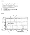
- the method of the first aspect of the invention is a method of manufacturing a PZT-based ferroelectric thin film 12 on a lower electrode 11 by coating, calcining, and then firing so as to crystallize a PZT-based ferroelectric thin film-forming composition on the lower electrode 11 of a substrate 10 having the lower electrode 11 in which a crystal plane is oriented in a (111) axis direction as shown in Figs.
- a first holding step 14 in which the temperature of the composition is increased from a temperature in a temperature range of 0°C to 150°C (or room temperature) and the composition is held at a temperature in a temperature range of 200°C to 350°C
- a second holding step 16 in which the temperature of the composition is increased from a holding temperature of the first holding step 14 and the composition is held at a temperature in a temperature range of 350°C to 500°C higher than the holding temperature of the first holding step 14 are included.
- the holding steps having a plurality of calcination temperatures including the first holding step 14 and the second holding step 16 are provided during the calcination (hereinafter referred to as the "two-step calcination”.
- calcination of the related art having a single-step holding will be referred to as the "one-step calcination"
- infrared rays are used as a heat source for calcination
- the progress of thermal decomposition, thermal expansion, thermal contraction, and the like during the calcination of the PZT-based ferroelectric thin film is set to be slow, and therefore it is possible to prevent cracking and provide a method of manufacturing a dense PZT-based ferroelectric thin film.
- the first temperature-increase rate 13 from the initial temperature, such as room temperature, to until the first holding step 14 is reached and until the temperature-increase rate 15 from the first holding step 14 to until the second holding step 16 is reached are set in the respective predetermined ranges, the occurrence of cracking derived from large stress generated due to an excess temperature-increase rate, abrupt thermal decomposition or degassing is prevented, and a denser PZT-based ferroelectric thin film can be obtained.
- the holding temperature until the firing is in a temperature range of 550°C to 800°C, and a temperature-increase rate through the holding time is in a range of 2.5°C/second to 150°C/second, thereby setting the temperature-increase rate from the second holding step 16 to the holding temperature of the firing in a predetermined range, the occurrence of cracking caused by thermal expansion and the like resulting from an excess temperature-increase rate, abrupt thermal decomposition or degassing is prevented, and a denser PZT-based ferroelectric thin film can be obtained.
- a PZT-based ferroelectric thin film-forming composition is prepared using an organic metal compound solution which contains raw materials for configuring a complex metal oxide dissolved in an organic solvent so as to obtain a ratio at which a desired metal atomic ratio is supplied.
- the "PZT-based" ferroelectric thin film includes ferroelectric compositions other than PZT, such as PLZT, PMnZT, and PNBZT.
- the raw material of the complex metal oxide is preferably a compound in which organic groups are bonded to the respective metal elements of Pb, La, Zr and Ti through oxygen or nitrogen atoms thereof.
- examples thereof include one or two or more selected from a group consisting of metal alkoxides, metal diol complexes, metal triol complexes, metal carboxylates, metal ⁇ -diketonate complexes, metal ⁇ -diketoester complexes, metal ⁇ -iminoketo complexes and metal amino complexes.
- a particularly preferable compound is a metal alkoxide, a partial hydrolysate thereof, an organic acid salt.
- examples of a Pb compound and a La compound include acetates (lead acetate: Pb(OA c ) 2 , lanthanum acetate: La(OA c ) 3 ), lead diisoproproxide: Pb(OiPr) 2 , lanthanum triisopropoxide: La(OiPr) 3 , and the like.
- Examples of a Ti compound include alkoxides such as titanium tetraethoxide: Ti(OEt) 4 , titanium tetraisopropoxide: Ti(OiPr) 4 , titanium tetra n-butoxide: Ti(OiBu) 4 , titanium tetraisobutoxide: Ti(OiBu) 4 , titanium tetra t-butoxide: Ti(OtBu) 4 , and titanium dimethoxy diisopropoxide: Ti(OMe) 2 (OiPr) 2 .
- alkoxides such as titanium tetraethoxide: Ti(OEt) 4 , titanium tetraisopropoxide: Ti(OiPr) 4 , titanium tetra n-butoxide: Ti(OiBu) 4 , titanium tetraisobutoxide: Ti(OiBu) 4 , titanium tetra t-butoxide: Ti(OtBu) 4 , and
- a composition for obtaining a concentration suitable for coating by dissolving the raw materials in an appropriate solvent at a ratio corresponding to the desired PZT-based ferroelectric thin film composition is preferably prepared in the following liquid synthesis flow.
- a Zr source, a Ti source and a stabilizer are put into a reaction vessel, and are refluxed in a nitrogen atmosphere.
- a Pb source is added to the refluxed compound, a solvent is added, the solution is refluxed in a nitrogen atmosphere, is distilled under reduced pressure so as to remove byproducts, then, propylene glycol is further added to the solution so as to adjust the concentration, and, furthermore, n-butanol is added to this solution.
- the solvent of the PZT-based ferroelectric thin film used here is appropriately determined depending on the raw materials to be used, and general examples thereof that can be used include carboxylic acids, alcohols (for example, propylene glycol which is a multivalent alcohol), esters, ketones (for example, acetone and methyl ethyl ketone), ethers (for example, dimethyl ether and diethyl ether), cycloalkanes (for example, cyclohexane and cyclohexanol), aromatic solvents (for example, benzene, toluene and xylene), other tetrahydrofuran, or a mixed solvent of two or more thereof.
- carboxylic acids for example, propylene glycol which is a multivalent alcohol
- esters for example, ketones (for example, acetone and methyl ethyl ketone), ethers (for example, dimethyl ether and diethyl ether), cycloalkanes (for example
- carboxylic acids that is preferably used include n-butyric acid, ⁇ -methyl butyric acid, i-valeric acid, 2-ethyl butyric acid, 2,2-dimethyl butyric acid, 3,3-dimethyl butyric acid, 2,3-dimethyl butyric acid, 3-methyl pentanoic acid, 4-methyl pentanoic acid, 2-ethyl pentanoic acid, 3-ethyl pentanoic acid, 2,2-dimethyl pentanoic acid, 3,3-dimethyl pentanoic acid, 2,3-dimethyl pentanoic acid, 2-ethyl hexanoic acid, and 3-ethyl hexanoic acid.
- ethyl acetate, propyl acetate, n-butyl acetate, sec-butyl acetate, tert-butyl acetate, isobutyl acetate, n-amyl acetate, sec-amyl acetate, tert-amyl acetate or isoamyl acetate is preferably used as the ester, and 1-propanol, 2-propanol, 1-butanol, 2-butanol, isobutyl alcohol, 1-pentanol, 2-pentanol, 2-methyl-2-pentanol, or 2-methoxy ethanol is preferably used as the alcohol.
- the total concentration of an organic metallic compound in the organic metal compound solution of the composition for forming the PZT-based ferroelectric thin film is preferably set to approximately 0.1 mass% to 23 mass% in terms of the amount of the metal oxide.
- a ⁇ -diketone for example, acetyl acetone, heptafluorobutanoyl pivaloyl methane, dipivaloyl methane, trifluoroacetyl acetone, benzoyl acetone, or the like
- a ⁇ -ketonic acid for example, acetoacetic acid, propionyl acetate, benzoyl acetate, or the like
- a ⁇ -ketoester for example, a lower alkyl ester such as methyl, propyl, or butyl of the above ketonic acid
- an oxyacid for example, lactic acid, glycolic acid, ⁇ -hydroxybutyric acid, salicylic acid, or the like
- a lower alkyl ester of the above oxyacid for example, oxyketone (for example, diacetone alcohol, acetoine, or the like), a diol, a triol, a higher carboxylic acid
- the PZT-based ferroelectric thin film-forming composition may include a ⁇ -diketone and a multivalent alcohol.
- a ⁇ -diketone is particularly preferable as the ⁇ -diketone
- propylene glycol is particularly preferable as the multivalent alcohol.
- a spin coating method which is a CSD method and uses a spin coater, is preferably used, the solution manufactured in the composition preparation step is added dropwise on a Pt film of the lower electrode in which a SiO 2 film, a TiO 2 film and a Pt film are sequentially formed on a Si substrate set on a spin coat, and spin coating is carried out at 1500 rpm to 2000 rpm for 60 seconds, thereby forming a coated film on the Pt substrate.
- the substrate on which the coated film is formed is disposed on a hot plate at 150°C, heated for 3 minutes, and a solvent having a low boiling point or adsorbed water molecules are removed, thereby making the coated film into a gel-stat film (hereinafter referred to as the "gel film").
- a solvent having a low boiling point or adsorbed water molecules are removed, thereby making the coated film into a gel-stat film (hereinafter referred to as the "gel film").
- Other CSD method other than the spin coating method such as a dip coating method or a Liquid Source Misted Chemical Deposition (LSMCD) method, may be appropriately applied instead of the spin coating.
- LSMCD Liquid Source Misted Chemical Deposition
- the calcination step In the calcination step, the solvent or moisture in the gel film are removed, and the organic metal compound is thermally decomposed or hydrolyzed so as to be converted into a complex oxide. Therefore, the calcination is carried out in the air, an oxidation atmosphere, or a water vapor-containing atmosphere.
- the "calcination step” is defined as a step for firing the gel film at a temperature lower than the temperature at which a perovskite phase begins to be formed in a desired PZT-based ferroelectric thin film as a phase of the complex oxide, and, meanwhile, the "firing step” described below is defined as a step for forming a perovskite phase in the PZT-based ferroelectric thin film.
- Fig. 2 is a temperature profile of the calcination step having parameters of the process time of calcination (seconds) in the horizontal axis and the calcination temperature (°C) in the vertical axis.
- the dashed line indicates the temperature profile of the two-step calcination of the embodiment, and the solid line indicates the temperature profile of a single-step calcination of a technique of the related art.
- the temperature is increased at a temperature-increase rate 17 at which the calcination temperature is monotonously and abruptly increased to the holding temperature (450°C in Fig. 2 ) using RTA in order for productivity improvement, and then, a holding temperature 18 is maintained for a certain holding time.
- calcination is carried out in a manner in which the holding temperature areas are provided at two places of the first holding step 14 and the second holding step 16, the temperature is increased from a relatively low certain temperature, such as room temperature, to the first holding step 14 at a very slow temperature-increase rate (a first temperature-increase rate 13) using RTA, and, furthermore, the temperature is increased from the first holding step 14 to the second holding step 16 at preferably the second temperature-increase rate 15 faster than the first temperature-increase rate.
- a relatively low certain temperature such as room temperature
- the number of the temperature holding steps is set to two, but the temperature holding steps may be provided at three or more preferable as necessary in consideration of the composition of the raw materials, the mixing of additives, and the like.
- infrared rays are used. For example, when a heater (not shown) generating infrared rays is disposed below the substrate 10, and then the gel film is heated, it is possible to remove (degas) remaining organic components from the gel film and to fire the composition while thermally decomposing, expanding, and contracting the gel film in a slow manner.
- the temperature in accordance which the two-step calcination profile shown in Fig. 2 can be controlled by disposing the substrate 10 on an infrared heater, not shown, and using a temperature controlling apparatus, not shown, connected to the infrared heater. According to such temperature control, it is possible to appropriately change conditions of the temperature profile including the temperature-increase rate, the holding temperature, and the holding time.
- a temperature profile of the two-step calcination in which any of three rates can be selected, is shown for the first temperature-increase rate during calcination in accordance with the temperature profile program-set in the temperature controlling apparatus in advance.
- the conditions and reasons for the temperature profile for carrying out the two-step calcination will be described below in detail.
- the main object of the first holding step is decomposition, combustion, and drying of a remaining organic substance such as a polymer or a solvent included in the solution of the PZT-based ferroelectric thin film composition. Therefore, when the holding temperature of the first holding step is too high, untargeted oxides are locally generated due to combustion and the like of the remaining organic component, and a dense and homogeneous film cannot be obtained. Therefore, the holding temperature is set to any of 200°C to 350°C (for example, 275°C) in the first holding step, and the composition is held for 1 minute to 5 minutes.
- the reason for the above is that decomposition of a precursor is not sufficiently accelerated at a holding temperature of the first holding step of lower than 200°C, and, when the holding temperature exceeds 350°C, decomposition proceeds too abruptly such that cracking occurs due to generation of voids derived from gas generation or stress derived from film contraction.
- the holding time of the first holding step is less than 1 minute, the precursor substance does not decompose sufficiently, and when the holding time exceeds 5 minutes, the productivity deteriorates.
- the holding temperature is preferably set to any of 250°C to 300°C, and the composition is preferably held for 3 minutes to 5 minutes.
- the holding temperature of the first holding step is lower than 250°C, decomposition of a polymer or the like included in the precursor becomes insufficient, and generation of voids and the like are induced due to generation of gas, and, when the holding temperature exceeds 300°C, thermal decomposition abruptly proceeds, and there is a concern that cracks or voids may be generated.
- the holding time of the first holding step is set to 1 minute to 5 minute. The reason for this is that, when the holding time of the first holding step is less than 1 minute, thermal decomposition is not sufficient, and, when the holding time exceeds 5 minutes, the productivity deteriorates.
- the temperature is increased from the temperature in a temperature range of 0°C to 150°C (or room temperature) to the holding temperature of the first holding step at a temperature-increase rate of 1°C/second to 50°C/second (the first temperature-increase rate).
- the first temperature-increase rate is preferably set to 2.5°C/second to 10°C/second. The reason for the above is that, when the first temperature-increase rate is less than 2.5°C/second, the productivity is poor, and, when the first temperature-increase rate exceeds 10°C/second, decomposition of the precursor abruptly proceeds excessively.
- the main object of the second holding step is removal of alkoxyl groups derived from a small amount of metal alkoxide, which cannot be removed in the first holding time, or organic ligands added as the stabilizer, or densification of an amorphous film. Therefore, in the second holding step, the holding temperature is set to any of 350°C to 500°C (for example, 450°C), and the composition is held for 5 minutes to 10 minutes.
- the reason for the above is that, when the holding temperature of the second holding step is lower than 350°C, unnecessary oxides are liable to be generated in the film if the decomposition is not sufficient, and, when the holding temperature exceeds 500°C, some of the film becomes a perovskite phase, and it becomes difficult to obtain an epitaxial-like film.
- the temperature is increased to the holding temperature of the second holding step at a temperature-increase rate of 1°C/second to 100°C/second (the second temperature-increase rate).
- the second temperature-increase rate is less than 1°C/second, the productivity is poor, and, when the second temperature-increase rate exceeds 100°C/second, untargeted oxides are generated in the film due to abrupt thermal decomposition.
- the second temperature-increase rate is preferably set to 2.5°C/second to 50°C/second.
- the reason for the above is that, when the second temperature-increase rate is less than 2.5°C/second, the productivity is poor, and, when the second temperature-increase rate exceeds 50°C/second, decomposition of the precursor substance abruptly proceeds, and densification does not proceed.
- the holding time of the second holding step is set to 3 minutes to 20 minutes in order to sufficiently promote making the PZT-based ferroelectric thin film amorphous. The reason for this is that, when the holding time of the second holding step is less than 3 minutes, thermal decomposition of the precursor is not sufficient, and, when the holding time exceeds 3 minutes, the reaction sufficiently proceeds.
- the holding time of the second holding step is set to 3 minutes to 10 minutes.
- the reason for this is that, when the holding time of the second holding step is less than 3 minutes, thermal decomposition of the precursor is not sufficient, and, when the holding time exceeds 10 minutes, thermal decomposition is almost completed, and there is no large influence on the orientation of the film and the like.
- the firing step is a step for firing the thin film of a PZT-based ferroelectric body obtained in the calcination step at a temperature which is the crystallization temperature or higher so as to crystallize the thin film, and a PZT-based ferroelectric thin film having a perovskite phase is obtained through this step.
- the firing atmosphere in the crystallization process is preferably O 2 , N 2 , Ar, N 2 O, H 2 , or a gas mixture thereof.
- the firing is carried out at 450°C to 800°C for 1 minute to 60 minutes, and it is also possible to employ an RTA treatment in order to increase the production efficiency.
- the reason for the above is that, when the firing temperature is lower than 450°C, a perovskite phase cannot be obtained, and, when the firing temperature exceeds 800°C, the film characteristics deteriorate.
- the firing time is less than 1 minute, the firing is not sufficient, and, when the firing time exceeds 60 minutes, the productivity deteriorates.
- the firing temperature and the firing time are preferably 600°C to 700°C and 1 minute to 5 minutes.
- the temperature-increase rate is set to 2.5°C/second to 150°C/second. In this case, the temperature-increase rate is preferably set to 10°C/second to 100°C/second. This is because, when the temperature-increase rate is less than 10°C/second, the productivity is poor, and, when the temperature-increase rate exceeds 100°C/second, it is difficult to control firing-related apparatuses.
- the PZT-based ferroelectric thin film manufactured using the embodiment in the above manner can be used for a complex electronic component, such as a thin film capacitor, a capacitor, an IPD, a DRAM memory capacitor, a laminate capacitor, a gate insulator of a transistor, a non-volatile memory, a pyroelectric infrared detecting element, a piezoelectric element, an electro-optic element, an actuator, a resonator, an ultrasonic motor, or an LC noise filter element.
- a complex electronic component such as a thin film capacitor, a capacitor, an IPD, a DRAM memory capacitor, a laminate capacitor, a gate insulator of a transistor, a non-volatile memory, a pyroelectric infrared detecting element, a piezoelectric element, an electro-optic element, an actuator, a resonator, an ultrasonic motor, or an LC noise filter element.
- 16 PZT-based ferroelectric thin films were obtained using a composition preparation step, a coating step, a calcination step through two-step calcination using infrared rays, and a firing step.
- 5 PZT-based ferroelectric thin films were obtained using a composition preparation step, a coating step, a calcination step not provided with a holding step of the related art, and a firing step.
- the conditions for the first holding temperatures, the first temperature-increase rates, the second holding temperatures, and the second temperature-increase rates in the calcination steps of the examples were summarized in Tables 1 and 2.
- Tables 1 and 2 summarize the values of the film thicknesses and the refractive indexes for the respective conditions after calcination and after firing, and the measuring method, the evaluation method, and the evaluation results will be described below.
- composition preparation step and the coating step are steps commonly included in all of the examples and the comparative examples, and were carried out in the following manner.
- polyvinylpyrrolidone was added to this raw material solution so that the molar ratio of PZT:polyvinylpyrrolidone became 1:0.5, and the solution was stirred for 24 hours at room temperature.
- N-methylformamide was added to the raw material solution so that the concentration became 7 wt%, the solution was stirred for 2 hours, and stabilized for 24 hours at room temperature.
- the solution obtained in the composition preparation step was added dropwise on a Si/SiO 2 /TiO 2 /Pt substrate set on a spin coater, and spin coating was carried out at 2000 rpm for 60 seconds, thereby forming a coated film.
- the coated film which was about to undergo the calcination step was heated on a hot plate at 150°C for 3 minutes, and the solvent having a low boiling point or absorbed moisture was removed, thereby obtaining a gel film.
- Example 1 the gel film obtained in the coating step was calcined using infrared rays in the calcination step of two-step calcination.
- the temperature was increased from 25°C to 275° at a temperature-increase rate of 1°C/second, the gel film was held for 3 minutes, the temperature was increased to 450°C at a temperature-increase rate of 2.5°C/second, and the gel film was held for 5 minutes.
- the amorphous film obtained in the calcination step was fired at a temperature-increase rate of5°C/second and 700° for 5 minutes, and a PZT-based ferroelectric thin film was obtained.
- Example 2 the gel film obtained in the coating step was calcined using infrared rays in the calcination step of two-step calcination.
- the temperature was increased from 25°C to 275°C at a temperature-increase rate of 1°C/second, the gel film was held for 3 minutes, the temperature was increased to 450°C at a temperature-increase rate of10°C/second, and the gel film was held for 5 minutes.
- the amorphous film obtained in the calcination step was fired at a temperature-increase rate of 5°C/second and 700°C for 5 minutes, and a PZT-based ferroelectric thin film was obtained.
- Example 3 the gel film obtained in the coating step was calcined using infrared rays in the calcination step of two-step calcination.
- the temperature was increased from 25°C to 275° at a temperature-increase rate of 1°C/second, the gel film was held for 3 undergo the temperature was increased to 450°C at a temperature-increase rate of 25°C/second, and the gel film was held for 5 minutes.
- the firing undergo the amorphous film obtained in undergo the step was fired at a temperature-increase rate of 5°C/second and 700° for 5 minutes, and a PZT-based ferroelectric thin film was obtained.
- Example 4 the gel film obtained in the coating step was calcined using infrared rays in the calcination step of two-step calcination.
- the temperature was increased from 25°C to 275° at a temperature-increase rate of 1°C/second, the gel film was held for 3 undergo the temperature was increased to 450°C at a temperature-increase rate of 50°C/second, and the gel film was held for 5 minutes.
- the amorphous film obtained in the calcination step was fired at a temperature-increase rate of 5°C/second and 700°C for 5 minutes, and a PZT-based ferroelectric thin film was obtained.
- Example 5 the gel film obtained in the coating step was calcined using infrared rays in the calcination step of two-step calcination.
- the temperature was increased from 25°C to 275°C at a temperature-increase rate of 2.5°C/second, the gel film was held for 3 undergo the temperature was increased to 450°C at a temperature-increase rate of 2.5°C/second, and the gel film was held for 5 minutes.
- inthe firing undergo the film obtained in the calcination step was fired at a temperature-increase rate of 5°C/second and 700°C for 5 minutes, and a PZT-based ferroelectric thin film was obtained.
- Example 6 the gel film obtained in the coating step was calcined using infrared rays in the calcination step of two-step calcination.
- the temperature was increased from 25°C to 275°C at a temperature-increase rate of 2.5°C/second, the gel film was held for 3 minutes, the temperature was increased to 450°C at a temperature-increase rate of10°C/second, and the gel film was held for 5 minutes.
- the amorphous film obtained in the calcination step was fired at a temperature-increase rate of 5°C/second and 700°C for 5 minutes, and a PZT-based ferroelectric thin film was obtained.
- Example 7 the gel film obtained in the coating step was calcined using infrared rays the calcination step of two-step calcination.
- the temperature was increased from 25°C to 275° at a temperature-increase rate of 2.5°C/second, the gel film was held for 3 minutes, the temperature was increased to 450°C at a temperature-increase rate of 10°C/second, and the gel film was held for 5 minutes.
- the firing step the amorphous film obtained in the calcination step was fired at a temperature-increase rate of 5°C/second and 700°C for 5 minutes, and a PZT-based ferroelectric thin film was obtained.
- Example 8 the gel film obtained in the coating step was calcined using infrared rays in the calcination step of two-step calcination.
- the temperature was increased from 25° to 275°C at a temperature-increase rate of 2.5°C/second, the gel film was held for 3 minutes, the temperature was increased to 450°C at a temperature-increase rate of 50°C/second, and the gel film was held for 5 minutes.
- the amorphous film obtained in the calcination step was fired at a temperature-increase rate of 5°C/second and 700° for 5 minutes, and a PZT-based ferroelectric thin film was obtained.
- Example 9 the gel film obtained in the coating step was calcined using infrared rays in the calcination step of two-step calcination.
- the temperature was increased from 25°C to 275°C at a temperature-increase rate of 10°C/second, the gel film was held for 3 minutes, the temperature was increased to 450°C at a temperature-increase rate of 2.5°C/second, and the gel film was held for 5 minutes.
- the amorphous film obtained in the calcination step was fired at a temperature-increase rate of 5°C/second and 700°C for 5 minutes, and a PZT-based ferroelectric thin film. was obtained.
- Example 10 the gel film obtained in the coating step was calcined using infrared rays in the calcination step of two-step calcination.
- the temperature was increased from 25°C to 275°C at a temperature-increase rate of 10°C/second, the gel film was held for 3 minutes, the temperature was increased to 450°C at a temperature-increase rate of10°C/second, and the gel film was held for 5 minutes.
- the amorphous film obtained in the calcination step was fired at a temperature-increase rate of 5°C/second and 700°C for 5 minutes, and a PZT-based ferroelectric thin film was obtained.
- Example 11 the gel film obtained in the coating step was calcined using infrared rays in the calcination step of two-step calcination.
- the temperature was increased from 25°C to 275°C at a temperature-increase rate of 10°C/second, the gel film was held for 3 minutes, the temperature was increased to 450°C at a temperature-increase rate of 25°C/second, and the gel film was held for 5 minutes.
- the amorphous film obtained in the calcination step was fired at a temperature-increase rate of 5°C/second and 700° for 5 minutes, and a PZT-based ferroelectric thin film was obtained.
- Example 12 the gel film. obtained in the coating step was calcined using infrared rays in the calcination step of two-step calcination.
- the temperature was increased from 25°C to 275° at a temperature-increase rate of 10°C/second, the gel film was held for 3 minutes, the temperature was increased to 450°C at a temperature-increase rate of 50°C/second, and the gel film was held for 5 minutes.
- the amorphous film obtained in the calcination step was fired at a temperature-increase rate of 5°C/second and 700°C for 5 minutes, and a PZT-based ferroelectric thin film was obtained.
- Example 13 the gel film. obtained in the coating step was calcined using infrared rays in the calcination step of two-step calcination.
- the temperature was increased from 25°C to 275°C at a temperature-increase rate of 2.5°C/second, the gel film was held for 3 minutes, the temperature was increased to 450°C at a temperature-increase rate of 10°C/second, and the gel film was held for 5 minutes.
- the amorphous film obtained in the calcination step was fired at a temperature-increase rate of 5°C/second and 700°C for 5 minutes, and a PZT-based ferroelectric thin film was obtained.
- Example 14 the gel film obtained in the coating step was calcined using infrared rays in the calcination step of two-step calcination.
- the temperature was increased from 25°C to 300°C at a temperature-increase rate of 2.5°C/second, the gel film was held for 3 minutes, the temperature was increased to 450°C at a temperature-increase rate of 10°C/second, and the gel film was held for 5 minutes.
- the firing step the amorphous film obtained in the calcination step was fired at a temperature-increase rate of 5°C/second and 700°C for 5 minutes, and a PZT-based ferroelectric thin film was obtained.
- Example 15 the gel film obtained in the coating step was calcined using infrared rays in the calcination step of two-step calcination.
- the temperature was increased from 25° to 275°C at a temperature-increase rate of 2.5°C/second, the gel film was held for 3 minutes, the temperature was increased to 425°C at a temperature-increase rate of 10°C/second, and the gel film was held for 5 minutes.
- the amorphous film obtained in the calcination step was fired at a temperature-increase rate of 5°C/second and 700°C for 5 minutes, and a PZT-based ferroelectric thin film was obtained.
- Example 16 the gel film obtained in the coating step was calcined using infrared rays in the calcination step of two-step calcination.
- the temperature was increased from 25°C to 275°C at a temperature-increase rate oaf 2.5°C/second, the gel film was held for 3 minutes, the temperature was increased to 475°C at a temperature-increase rate of 10°C/second, and the gel film was held for 5 minutes.
- the amorphous film obtained in the calcination step was fired at a temperature-increase rate of 5°C/second and 700°C for 5 minutes, and a PZT-based ferroelectric thin film was obtained.
- the temperature of the gel film obtained in the coating step was increased to 400°C at a temperature-increase rate of 10°C/second in the calcination step of a single-step calcination of the related art, the gel film was held at this temperature for 8 minutes so as to be calcined, and then, in the firing step, the film obtained in the calcination step was fired under conditions of a temperature-increase rate of 10°C/second and 700°C for 5 minuted, thereby obtaining a PZT-based ferroelectric thin film.
- the temperature of the gel film obtained in the coating step was increased to 450°C at a temperature-increase rate of 10°C/second in the calcination step of a single-step calcination of the related art, the gel film was held at this temperature for 8 minutes so as to be calcined, and then, in the firing step, the film obtained in the calcination step was fired under conditions of a temperature-increase rate of 10°C/second and 700°C for 5 minutes, thereby obtaining a PZT-based ferroelectric thin film.
- the temperature of the gel film obtained in the coating step was increased to 475°C at a temperature-increase rate of 10°C/second in the calcination step of a single-step calcination of the related art, the gel film was held at this temperature for 8 minutes so as to be calcined, and then, in the firing step, the film obtained in the calcination step was fired under conditions of a temperature-increase rate of 10°C/second and 700°C for 5 minutes, thereby obtaining a PZT-based ferroelectric thin film.
- the temperature of the gel film obtained in the coating step was increased to 500°C at a temperature-increase rate of 10°C/second in the calcination step of a single-step calcination of the related at the gel film was held at this temperature for 8 minutes so as to be calcined, and then, in the fiding step, the film obtained in the calcination step was fired under conditions of a temperature-increase rate of 10°C/second and 700°C for 5 minutes, thereby obtaining a PZT-based ferroelectric thin film.
- the temperature of the gel film obtained in the coating step was increased to 450°C at a temperature-increase rate of 2.5°C/second in the calcination step of a single-step calcination of the related art, the gel film was held at this temperature for 8 minutes so as to be calcined, and then, in the firing step, the film obtained in the calcination step was fired under conditions of a temperature-increase rate of 10°C/second and 700°C for 5 minutes, thereby obtaining a PZT-based ferroelectric thin film.
- the temperature of the gel film obtained in the coating step was increased to 450°C at a temperature-increase rate of 50°C/second in the calcination step of a single-step calcination of the related art, the gel film was held at this temperature for 8 minutes so as to be calcined, and then, in the firing step, the film obtained in the calcination step was fired under conditions of a temperature-increase rate of 10°C/second and 700°C for 5 minuted, thereby obtaining and a PZT-basedferroelectric thin film.
- the layer thicknesses and refractive indexes of the thin films after calcination and after firing were obtained using the following method, The results are shown in Table 1.
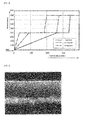
- the cross-sectional SEM image (a magnification of 100,000 times) of Example 6 and the cross-sectional SEM image (a magnification of 100,000 times) of Comparative example 6 are shown in Figs. 4 and 5 respectively,
- the XRD charts of Example 6 and Comparative example 2 are shown in Fig. 6 .
- the layer thicknesses after calcination become thinner in Examples 1 to 16 than in Comparative examples 1 to 6. This is considered to indicate that the PZT-based ferroelectric thin films obtained by calcining the gel films of Examples 1 to 16 become dense.
- the difference between the layer thickness after calcined, and the layer thickness after firing becomes smaller in Examples 1 to 16 than in Comparative examples 1 to 6.
- Examples 1 to 16 generally have higher values than Comparative examples 1 to 6. This is considered to be because the crystallinity is improved and the refractive index is improved by carrying out two-step calcination.
- the layer thicknesses and the refractive indexes are considered with reference to Tables 1 and 2 for Examples 4, 8 and 12 which follow the temperature profile of the two-step calcination step as shown in Fig. 3 .
- the first temperature-increase rates are 1 °C/second, 2.5°C/second, and 10°C/second
- the first holding temperatures are 275°C
- the second temperature-increase rates are 50°C/second
- the second holding temperatures are 450°C.
- the layer thicknesses after calcination of Examples 4, 8 and 12 were 366 nm, 382 nm, and 389 nm, the layer thicknesses after firing were 314 nm, 331 nm, and 314 nm respectively, and there was a tendency for the layer thicknesses after calcination to increase as the first temperature-increase rate increases, however, there was no significant difference in the layer thicknesses after firing.
- the refractive indexes after calcination in Examples 4, 8 and 12 were 2.21, 2.26 and 2,24, the refractive indexes after firing were 2.44, 2.46 and 2.46 respectively, and there was no significant difference between the examples.
- the temperature-increase rate is preferably high; however, when the temperature-increase rate is set to too large, a problem of the related art, such as the occurrence of cracking, may occur, which is considered to be not preferable.
- Examples 1 to 16 had favorable crystallinity, but Comparative examples 1 to 6 were film which were not oriented and had a low crystallinity. Thereby, it was found that a dense and highly crystalline film can be obtained by introducing two-step calcination using infrared rays.
- the method of manufacturing a PZT-based ferroelectric thin film of the invention enables coating, calcination, and firing at a thickness per layer approximately 5 times to 10 times the thickness per layer in the manufacturing method of the related art, and can provide a PZT-based ferroelectric thin film which is preferable for use in which a film thickness of 1 ⁇ m to 3 ⁇ m is required, for example, thin film piezoelectric use, at a low cost, dense, and excellent in terms of crystallinity.
Landscapes
- Engineering & Computer Science (AREA)
- Chemical & Material Sciences (AREA)
- Power Engineering (AREA)
- Ceramic Engineering (AREA)
- Manufacturing & Machinery (AREA)
- Microelectronics & Electronic Packaging (AREA)
- Inorganic Chemistry (AREA)
- Materials Engineering (AREA)
- Organic Chemistry (AREA)
- Metallurgy (AREA)
- Physics & Mathematics (AREA)
- Thermal Sciences (AREA)
- General Chemical & Material Sciences (AREA)
- Chemical Kinetics & Catalysis (AREA)
- Mechanical Engineering (AREA)
- Dispersion Chemistry (AREA)
- Structural Engineering (AREA)
- Composite Materials (AREA)
- Semiconductor Memories (AREA)
- Formation Of Insulating Films (AREA)
- Non-Volatile Memory (AREA)
- Inorganic Compounds Of Heavy Metals (AREA)
- Ceramic Capacitors (AREA)
- Fixed Capacitors And Capacitor Manufacturing Machines (AREA)
- Inorganic Insulating Materials (AREA)
Applications Claiming Priority (1)
| Application Number | Priority Date | Filing Date | Title |
|---|---|---|---|
| JP2012078916A JP5919956B2 (ja) | 2012-03-30 | 2012-03-30 | Pzt系強誘電体薄膜の製造方法 |
Publications (3)
| Publication Number | Publication Date |
|---|---|
| EP2645441A2 true EP2645441A2 (de) | 2013-10-02 |
| EP2645441A3 EP2645441A3 (de) | 2015-01-28 |
| EP2645441B1 EP2645441B1 (de) | 2016-12-14 |
Family
ID=47913302
Family Applications (1)
| Application Number | Title | Priority Date | Filing Date |
|---|---|---|---|
| EP13161001.6A Active EP2645441B1 (de) | 2012-03-30 | 2013-03-26 | Verfahren zur Herstellung einer ferroelektrischen Dünnschicht auf PZT-Basis |
Country Status (6)
| Country | Link |
|---|---|
| US (1) | US20130260142A1 (de) |
| EP (1) | EP2645441B1 (de) |
| JP (1) | JP5919956B2 (de) |
| KR (1) | KR101934124B1 (de) |
| CN (1) | CN103359785A (de) |
| TW (1) | TWI586628B (de) |
Cited By (1)
| Publication number | Priority date | Publication date | Assignee | Title |
|---|---|---|---|---|
| EP3125317A4 (de) * | 2014-03-27 | 2017-11-08 | Mitsubishi Materials Corporation | Zusammensetzung zur bildung von mn-dotierter, pzt-basierter piezoelektrischer folie und mn-dotierte, pzt-basierte piezoelektrische folie |
Families Citing this family (7)
| Publication number | Priority date | Publication date | Assignee | Title |
|---|---|---|---|---|
| JP6119288B2 (ja) * | 2013-02-14 | 2017-04-26 | 株式会社リコー | 強誘電体膜の形成方法 |
| JP6459563B2 (ja) * | 2014-03-27 | 2019-01-30 | 三菱マテリアル株式会社 | Pzt系強誘電体薄膜及びその形成方法 |
| US10112872B2 (en) | 2014-03-28 | 2018-10-30 | Mitsubishi Materials Corporation | Composition for forming Mn and Nb co-doped PZT-based piezoelectric film |
| JP6237407B2 (ja) * | 2014-03-28 | 2017-11-29 | 三菱マテリアル株式会社 | Mn及びNbドープのPZT系圧電体膜の形成方法 |
| CN105680718B (zh) * | 2016-04-11 | 2017-08-25 | 哈尔滨工业大学 | 蛙型一阶纵振直线超声电机 |
| CN106518069B (zh) * | 2016-09-29 | 2019-10-29 | 广东工业大学 | 一种掺镧锆钛酸铅铁电厚膜陶瓷材料及其制备方法 |
| KR102380663B1 (ko) | 2020-05-11 | 2022-03-29 | 김조희 | 해수수족관 정화용 스키머 |
Citations (1)
| Publication number | Priority date | Publication date | Assignee | Title |
|---|---|---|---|---|
| JP2001261338A (ja) | 2000-03-15 | 2001-09-26 | Mitsubishi Materials Corp | Tiを含有する金属酸化物薄膜形成用原料溶液、Tiを含有する金属酸化物薄膜の形成方法及びTiを含有する金属酸化物薄膜 |
Family Cites Families (10)
| Publication number | Priority date | Publication date | Assignee | Title |
|---|---|---|---|---|
| JPH04259380A (ja) * | 1991-02-13 | 1992-09-14 | Mitsubishi Materials Corp | Pzt強誘電体薄膜の結晶配向性制御方法 |
| JP4146533B2 (ja) * | 1997-08-21 | 2008-09-10 | ローム株式会社 | 強誘電体膜形成用溶液および強誘電体膜の形成法 |
| US6441415B1 (en) * | 1999-06-25 | 2002-08-27 | Texas Instruments Incorporated | Ferroelectric and paraelectric thin film devices using dopants which eliminate ferroelectricity |
| US6686236B2 (en) * | 2001-12-21 | 2004-02-03 | Texas Instruments Incorporated | Methods of preventing reduction of IrOx during PZT formation by metalorganic chemical vapor deposition or other processing |
| US6635497B2 (en) * | 2001-12-21 | 2003-10-21 | Texas Instruments Incorporated | Methods of preventing reduction of IrOx during PZT formation by metalorganic chemical vapor deposition or other processing |
| JP5013035B2 (ja) * | 2003-12-11 | 2012-08-29 | セイコーエプソン株式会社 | 誘電体膜の製造方法及び液体噴射ヘッドの製造方法 |
| JP2009070926A (ja) * | 2007-09-11 | 2009-04-02 | Tokyo Institute Of Technology | ペロブスカイト型酸化物薄膜の成膜方法および積層体 |
| JP5187489B2 (ja) * | 2007-09-20 | 2013-04-24 | セイコーエプソン株式会社 | アクチュエータ装置の製造方法及び液体噴射ヘッドの製造方法 |
| JP5533622B2 (ja) * | 2010-04-14 | 2014-06-25 | 三菱マテリアル株式会社 | 強誘電体薄膜形成用組成物、強誘電体薄膜の形成方法並びに該方法により形成された強誘電体薄膜 |
| JP5699297B2 (ja) * | 2010-04-28 | 2015-04-08 | 株式会社ユーテック | 基板処理装置及び薄膜の製造方法 |
-
2012
- 2012-03-30 JP JP2012078916A patent/JP5919956B2/ja not_active Expired - Fee Related
-
2013
- 2013-01-28 TW TW102103139A patent/TWI586628B/zh active
- 2013-03-14 US US13/829,507 patent/US20130260142A1/en not_active Abandoned
- 2013-03-15 KR KR1020130027976A patent/KR101934124B1/ko not_active Expired - Fee Related
- 2013-03-18 CN CN2013100851659A patent/CN103359785A/zh active Pending
- 2013-03-26 EP EP13161001.6A patent/EP2645441B1/de active Active
Patent Citations (1)
| Publication number | Priority date | Publication date | Assignee | Title |
|---|---|---|---|---|
| JP2001261338A (ja) | 2000-03-15 | 2001-09-26 | Mitsubishi Materials Corp | Tiを含有する金属酸化物薄膜形成用原料溶液、Tiを含有する金属酸化物薄膜の形成方法及びTiを含有する金属酸化物薄膜 |
Non-Patent Citations (2)
| Title |
|---|
| "Collection of know-how for controlling structures in a sol-gel method for achieving objects", TECHNICAL INFORMATION INSTITUTE CO., LTD., pages: 60 - 63 |
| JSOL-GEL TECHNOL, vol. 47, 2008, pages 316 - 325 |
Cited By (2)
| Publication number | Priority date | Publication date | Assignee | Title |
|---|---|---|---|---|
| EP3125317A4 (de) * | 2014-03-27 | 2017-11-08 | Mitsubishi Materials Corporation | Zusammensetzung zur bildung von mn-dotierter, pzt-basierter piezoelektrischer folie und mn-dotierte, pzt-basierte piezoelektrische folie |
| US10411183B2 (en) | 2014-03-27 | 2019-09-10 | Mitsubishi Materials Corporation | Composition for forming Mn-doped PZT-based piezoelectric film and Mn-doped PZT-based piezoelectric film |
Also Published As
| Publication number | Publication date |
|---|---|
| JP2013211306A (ja) | 2013-10-10 |
| EP2645441B1 (de) | 2016-12-14 |
| JP5919956B2 (ja) | 2016-05-18 |
| CN103359785A (zh) | 2013-10-23 |
| TW201343602A (zh) | 2013-11-01 |
| KR20130111304A (ko) | 2013-10-10 |
| EP2645441A3 (de) | 2015-01-28 |
| KR101934124B1 (ko) | 2018-12-31 |
| TWI586628B (zh) | 2017-06-11 |
| US20130260142A1 (en) | 2013-10-03 |
Similar Documents
| Publication | Publication Date | Title |
|---|---|---|
| EP2645441B1 (de) | Verfahren zur Herstellung einer ferroelektrischen Dünnschicht auf PZT-Basis | |
| KR101970832B1 (ko) | 강유전체 박막의 제조 방법 | |
| EP2525393B1 (de) | Verfahren zur Herstellung einer ferroelektrischen Dünnschicht | |
| KR102007543B1 (ko) | PNbZT 강유전체 박막의 제조 방법 | |
| EP2645440A2 (de) | Dünnschicht auf PZT-Basis und Verfahren zur Herstellung dafür | |
| EP2645439A2 (de) | Dünnschicht auf PZT-Basis und Verfahren zur Herstellung dafür | |
| KR102019522B1 (ko) | Pzt계 강유전체 박막 형성용 조성물 및 그 제조 방법 그리고 그 조성물을 사용한 pzt계 강유전체 박막의 형성 방법 | |
| JP6481394B2 (ja) | MnドープのPZT系圧電体膜 | |
| JP5655272B2 (ja) | 強誘電体薄膜形成用組成物、強誘電体薄膜の形成方法並びに該方法により形成された強誘電体薄膜 | |
| JP6787172B2 (ja) | Pzt系強誘電体薄膜及びその製造方法 | |
| KR20140118725A (ko) | Pzt 계 강유전체 박막 형성용 조성물 및 그 제조 방법 그리고 그 조성물을 사용한 pzt 계 강유전체 박막의 형성 방법 | |
| JP5526591B2 (ja) | 強誘電体薄膜形成用組成物、強誘電体薄膜の形成方法並びに該方法により形成された強誘電体薄膜 | |
| JP5659457B2 (ja) | 強誘電体薄膜形成用組成物、強誘電体薄膜の形成方法並びに該方法により形成された強誘電体薄膜 | |
| JP5417962B2 (ja) | 強誘電体薄膜形成用組成物、強誘電体薄膜の形成方法並びに該方法により形成された強誘電体薄膜 | |
| JP5644975B2 (ja) | Pzt強誘電体薄膜の製造方法 | |
| JP5293347B2 (ja) | 強誘電体薄膜形成用組成物、強誘電体薄膜の形成方法並びに該方法により形成された強誘電体薄膜 |
Legal Events
| Date | Code | Title | Description |
|---|---|---|---|
| PUAI | Public reference made under article 153(3) epc to a published international application that has entered the european phase |
Free format text: ORIGINAL CODE: 0009012 |
|
| AK | Designated contracting states |
Kind code of ref document: A2 Designated state(s): AL AT BE BG CH CY CZ DE DK EE ES FI FR GB GR HR HU IE IS IT LI LT LU LV MC MK MT NL NO PL PT RO RS SE SI SK SM TR |
|
| AX | Request for extension of the european patent |
Extension state: BA ME |
|
| PUAL | Search report despatched |
Free format text: ORIGINAL CODE: 0009013 |
|
| AK | Designated contracting states |
Kind code of ref document: A3 Designated state(s): AL AT BE BG CH CY CZ DE DK EE ES FI FR GB GR HR HU IE IS IT LI LT LU LV MC MK MT NL NO PL PT RO RS SE SI SK SM TR |
|
| AX | Request for extension of the european patent |
Extension state: BA ME |
|
| RIC1 | Information provided on ipc code assigned before grant |
Ipc: H01L 45/00 20060101AFI20141223BHEP Ipc: G02F 1/055 20060101ALI20141223BHEP Ipc: H01G 4/12 20060101ALI20141223BHEP Ipc: H01L 37/02 20060101ALI20141223BHEP Ipc: H02N 2/00 20060101ALI20141223BHEP Ipc: H01L 41/09 20060101ALI20141223BHEP Ipc: H01G 7/06 20060101ALI20141223BHEP Ipc: H01L 29/78 20060101ALI20141223BHEP Ipc: C23C 18/12 20060101ALI20141223BHEP Ipc: H03H 9/02 20060101ALI20141223BHEP Ipc: H01L 41/187 20060101ALI20141223BHEP Ipc: H01L 41/318 20130101ALI20141223BHEP Ipc: H01G 4/33 20060101ALI20141223BHEP |
|
| 17P | Request for examination filed |
Effective date: 20150623 |
|
| RBV | Designated contracting states (corrected) |
Designated state(s): AL AT BE BG CH CY CZ DE DK EE ES FI FR GB GR HR HU IE IS IT LI LT LU LV MC MK MT NL NO PL PT RO RS SE SI SK SM TR |
|
| 17Q | First examination report despatched |
Effective date: 20160104 |
|
| GRAP | Despatch of communication of intention to grant a patent |
Free format text: ORIGINAL CODE: EPIDOSNIGR1 |
|
| INTG | Intention to grant announced |
Effective date: 20160711 |
|
| GRAS | Grant fee paid |
Free format text: ORIGINAL CODE: EPIDOSNIGR3 |
|
| GRAA | (expected) grant |
Free format text: ORIGINAL CODE: 0009210 |
|
| AK | Designated contracting states |
Kind code of ref document: B1 Designated state(s): AL AT BE BG CH CY CZ DE DK EE ES FI FR GB GR HR HU IE IS IT LI LT LU LV MC MK MT NL NO PL PT RO RS SE SI SK SM TR |
|
| REG | Reference to a national code |
Ref country code: GB Ref legal event code: FG4D |
|
| REG | Reference to a national code |
Ref country code: CH Ref legal event code: EP |
|
| REG | Reference to a national code |
Ref country code: IE Ref legal event code: FG4D |
|
| REG | Reference to a national code |
Ref country code: AT Ref legal event code: REF Ref document number: 854302 Country of ref document: AT Kind code of ref document: T Effective date: 20170115 |
|
| REG | Reference to a national code |
Ref country code: NO Ref legal event code: T2 Effective date: 20161214 |
|
| REG | Reference to a national code |
Ref country code: DE Ref legal event code: R096 Ref document number: 602013015247 Country of ref document: DE |
|
| PG25 | Lapsed in a contracting state [announced via postgrant information from national office to epo] |
Ref country code: LV Free format text: LAPSE BECAUSE OF FAILURE TO SUBMIT A TRANSLATION OF THE DESCRIPTION OR TO PAY THE FEE WITHIN THE PRESCRIBED TIME-LIMIT Effective date: 20161214 |
|
| REG | Reference to a national code |
Ref country code: NL Ref legal event code: FP |
|
| REG | Reference to a national code |
Ref country code: SE Ref legal event code: TRGR |
|
| REG | Reference to a national code |
Ref country code: FR Ref legal event code: PLFP Year of fee payment: 5 |
|
| REG | Reference to a national code |
Ref country code: LT Ref legal event code: MG4D |
|
| PG25 | Lapsed in a contracting state [announced via postgrant information from national office to epo] |
Ref country code: GR Free format text: LAPSE BECAUSE OF FAILURE TO SUBMIT A TRANSLATION OF THE DESCRIPTION OR TO PAY THE FEE WITHIN THE PRESCRIBED TIME-LIMIT Effective date: 20170315 Ref country code: LT Free format text: LAPSE BECAUSE OF FAILURE TO SUBMIT A TRANSLATION OF THE DESCRIPTION OR TO PAY THE FEE WITHIN THE PRESCRIBED TIME-LIMIT Effective date: 20161214 |
|
| REG | Reference to a national code |
Ref country code: AT Ref legal event code: MK05 Ref document number: 854302 Country of ref document: AT Kind code of ref document: T Effective date: 20161214 |
|
| PG25 | Lapsed in a contracting state [announced via postgrant information from national office to epo] |
Ref country code: RS Free format text: LAPSE BECAUSE OF FAILURE TO SUBMIT A TRANSLATION OF THE DESCRIPTION OR TO PAY THE FEE WITHIN THE PRESCRIBED TIME-LIMIT Effective date: 20161214 Ref country code: HR Free format text: LAPSE BECAUSE OF FAILURE TO SUBMIT A TRANSLATION OF THE DESCRIPTION OR TO PAY THE FEE WITHIN THE PRESCRIBED TIME-LIMIT Effective date: 20161214 Ref country code: FI Free format text: LAPSE BECAUSE OF FAILURE TO SUBMIT A TRANSLATION OF THE DESCRIPTION OR TO PAY THE FEE WITHIN THE PRESCRIBED TIME-LIMIT Effective date: 20161214 |
|
| PG25 | Lapsed in a contracting state [announced via postgrant information from national office to epo] |
Ref country code: EE Free format text: LAPSE BECAUSE OF FAILURE TO SUBMIT A TRANSLATION OF THE DESCRIPTION OR TO PAY THE FEE WITHIN THE PRESCRIBED TIME-LIMIT Effective date: 20161214 Ref country code: IS Free format text: LAPSE BECAUSE OF FAILURE TO SUBMIT A TRANSLATION OF THE DESCRIPTION OR TO PAY THE FEE WITHIN THE PRESCRIBED TIME-LIMIT Effective date: 20170414 Ref country code: SK Free format text: LAPSE BECAUSE OF FAILURE TO SUBMIT A TRANSLATION OF THE DESCRIPTION OR TO PAY THE FEE WITHIN THE PRESCRIBED TIME-LIMIT Effective date: 20161214 Ref country code: CZ Free format text: LAPSE BECAUSE OF FAILURE TO SUBMIT A TRANSLATION OF THE DESCRIPTION OR TO PAY THE FEE WITHIN THE PRESCRIBED TIME-LIMIT Effective date: 20161214 Ref country code: RO Free format text: LAPSE BECAUSE OF FAILURE TO SUBMIT A TRANSLATION OF THE DESCRIPTION OR TO PAY THE FEE WITHIN THE PRESCRIBED TIME-LIMIT Effective date: 20161214 |
|
| PG25 | Lapsed in a contracting state [announced via postgrant information from national office to epo] |
Ref country code: ES Free format text: LAPSE BECAUSE OF FAILURE TO SUBMIT A TRANSLATION OF THE DESCRIPTION OR TO PAY THE FEE WITHIN THE PRESCRIBED TIME-LIMIT Effective date: 20161214 Ref country code: BE Free format text: LAPSE BECAUSE OF FAILURE TO SUBMIT A TRANSLATION OF THE DESCRIPTION OR TO PAY THE FEE WITHIN THE PRESCRIBED TIME-LIMIT Effective date: 20161214 Ref country code: PT Free format text: LAPSE BECAUSE OF FAILURE TO SUBMIT A TRANSLATION OF THE DESCRIPTION OR TO PAY THE FEE WITHIN THE PRESCRIBED TIME-LIMIT Effective date: 20170414 Ref country code: AT Free format text: LAPSE BECAUSE OF FAILURE TO SUBMIT A TRANSLATION OF THE DESCRIPTION OR TO PAY THE FEE WITHIN THE PRESCRIBED TIME-LIMIT Effective date: 20161214 Ref country code: SM Free format text: LAPSE BECAUSE OF FAILURE TO SUBMIT A TRANSLATION OF THE DESCRIPTION OR TO PAY THE FEE WITHIN THE PRESCRIBED TIME-LIMIT Effective date: 20161214 Ref country code: PL Free format text: LAPSE BECAUSE OF FAILURE TO SUBMIT A TRANSLATION OF THE DESCRIPTION OR TO PAY THE FEE WITHIN THE PRESCRIBED TIME-LIMIT Effective date: 20161214 Ref country code: BG Free format text: LAPSE BECAUSE OF FAILURE TO SUBMIT A TRANSLATION OF THE DESCRIPTION OR TO PAY THE FEE WITHIN THE PRESCRIBED TIME-LIMIT Effective date: 20170314 |
|
| REG | Reference to a national code |
Ref country code: DE Ref legal event code: R097 Ref document number: 602013015247 Country of ref document: DE |
|
| PLBE | No opposition filed within time limit |
Free format text: ORIGINAL CODE: 0009261 |
|
| STAA | Information on the status of an ep patent application or granted ep patent |
Free format text: STATUS: NO OPPOSITION FILED WITHIN TIME LIMIT |
|
| REG | Reference to a national code |
Ref country code: CH Ref legal event code: PL |
|
| 26N | No opposition filed |
Effective date: 20170915 |
|
| GBPC | Gb: european patent ceased through non-payment of renewal fee |
Effective date: 20170326 |
|
| PG25 | Lapsed in a contracting state [announced via postgrant information from national office to epo] |
Ref country code: MC Free format text: LAPSE BECAUSE OF FAILURE TO SUBMIT A TRANSLATION OF THE DESCRIPTION OR TO PAY THE FEE WITHIN THE PRESCRIBED TIME-LIMIT Effective date: 20161214 Ref country code: DK Free format text: LAPSE BECAUSE OF FAILURE TO SUBMIT A TRANSLATION OF THE DESCRIPTION OR TO PAY THE FEE WITHIN THE PRESCRIBED TIME-LIMIT Effective date: 20161214 |
|
| REG | Reference to a national code |
Ref country code: IE Ref legal event code: MM4A |
|
| PG25 | Lapsed in a contracting state [announced via postgrant information from national office to epo] |
Ref country code: LU Free format text: LAPSE BECAUSE OF NON-PAYMENT OF DUE FEES Effective date: 20170326 |
|
| PG25 | Lapsed in a contracting state [announced via postgrant information from national office to epo] |
Ref country code: LI Free format text: LAPSE BECAUSE OF NON-PAYMENT OF DUE FEES Effective date: 20170331 Ref country code: IE Free format text: LAPSE BECAUSE OF NON-PAYMENT OF DUE FEES Effective date: 20170326 Ref country code: GB Free format text: LAPSE BECAUSE OF NON-PAYMENT OF DUE FEES Effective date: 20170326 Ref country code: CH Free format text: LAPSE BECAUSE OF NON-PAYMENT OF DUE FEES Effective date: 20170331 Ref country code: SI Free format text: LAPSE BECAUSE OF FAILURE TO SUBMIT A TRANSLATION OF THE DESCRIPTION OR TO PAY THE FEE WITHIN THE PRESCRIBED TIME-LIMIT Effective date: 20161214 |
|
| REG | Reference to a national code |
Ref country code: FR Ref legal event code: PLFP Year of fee payment: 6 |
|
| PG25 | Lapsed in a contracting state [announced via postgrant information from national office to epo] |
Ref country code: MT Free format text: LAPSE BECAUSE OF NON-PAYMENT OF DUE FEES Effective date: 20170326 |
|
| PG25 | Lapsed in a contracting state [announced via postgrant information from national office to epo] |
Ref country code: HU Free format text: LAPSE BECAUSE OF FAILURE TO SUBMIT A TRANSLATION OF THE DESCRIPTION OR TO PAY THE FEE WITHIN THE PRESCRIBED TIME-LIMIT; INVALID AB INITIO Effective date: 20130326 |
|
| PG25 | Lapsed in a contracting state [announced via postgrant information from national office to epo] |
Ref country code: CY Free format text: LAPSE BECAUSE OF NON-PAYMENT OF DUE FEES Effective date: 20161214 |
|
| PG25 | Lapsed in a contracting state [announced via postgrant information from national office to epo] |
Ref country code: MK Free format text: LAPSE BECAUSE OF FAILURE TO SUBMIT A TRANSLATION OF THE DESCRIPTION OR TO PAY THE FEE WITHIN THE PRESCRIBED TIME-LIMIT Effective date: 20161214 |
|
| PG25 | Lapsed in a contracting state [announced via postgrant information from national office to epo] |
Ref country code: TR Free format text: LAPSE BECAUSE OF FAILURE TO SUBMIT A TRANSLATION OF THE DESCRIPTION OR TO PAY THE FEE WITHIN THE PRESCRIBED TIME-LIMIT Effective date: 20161214 |
|
| PG25 | Lapsed in a contracting state [announced via postgrant information from national office to epo] |
Ref country code: AL Free format text: LAPSE BECAUSE OF FAILURE TO SUBMIT A TRANSLATION OF THE DESCRIPTION OR TO PAY THE FEE WITHIN THE PRESCRIBED TIME-LIMIT Effective date: 20161214 |
|
| REG | Reference to a national code |
Ref country code: DE Ref legal event code: R079 Ref document number: 602013015247 Country of ref document: DE Free format text: PREVIOUS MAIN CLASS: H01L0045000000 Ipc: H10N0070000000 |
|
| PGFP | Annual fee paid to national office [announced via postgrant information from national office to epo] |
Ref country code: NL Payment date: 20240320 Year of fee payment: 12 |
|
| PGFP | Annual fee paid to national office [announced via postgrant information from national office to epo] |
Ref country code: DE Payment date: 20240320 Year of fee payment: 12 |
|
| PGFP | Annual fee paid to national office [announced via postgrant information from national office to epo] |
Ref country code: SE Payment date: 20240320 Year of fee payment: 12 Ref country code: NO Payment date: 20240322 Year of fee payment: 12 Ref country code: FR Payment date: 20240327 Year of fee payment: 12 |
|
| PGFP | Annual fee paid to national office [announced via postgrant information from national office to epo] |
Ref country code: IT Payment date: 20250325 Year of fee payment: 13 |
|
| REG | Reference to a national code |
Ref country code: DE Ref legal event code: R119 Ref document number: 602013015247 Country of ref document: DE |
|
| REG | Reference to a national code |
Ref country code: SE Ref legal event code: EUG |
|
| REG | Reference to a national code |
Ref country code: NL Ref legal event code: MM Effective date: 20250401 |
|
| PG25 | Lapsed in a contracting state [announced via postgrant information from national office to epo] |
Ref country code: NL Free format text: LAPSE BECAUSE OF NON-PAYMENT OF DUE FEES Effective date: 20250401 |
|
| PG25 | Lapsed in a contracting state [announced via postgrant information from national office to epo] |
Ref country code: DE Free format text: LAPSE BECAUSE OF NON-PAYMENT OF DUE FEES Effective date: 20251001 |
|
| PG25 | Lapsed in a contracting state [announced via postgrant information from national office to epo] |
Ref country code: NO Free format text: LAPSE BECAUSE OF NON-PAYMENT OF DUE FEES Effective date: 20250331 |
|
| PG25 | Lapsed in a contracting state [announced via postgrant information from national office to epo] |
Ref country code: FR Free format text: LAPSE BECAUSE OF NON-PAYMENT OF DUE FEES Effective date: 20250331 |
|
| PG25 | Lapsed in a contracting state [announced via postgrant information from national office to epo] |
Ref country code: SE Free format text: LAPSE BECAUSE OF NON-PAYMENT OF DUE FEES Effective date: 20250327 |