EP2628201B1 - Method for manufacturing an organic electronic device with encapsulation - Google Patents
Method for manufacturing an organic electronic device with encapsulation Download PDFInfo
- Publication number
- EP2628201B1 EP2628201B1 EP11773566.2A EP11773566A EP2628201B1 EP 2628201 B1 EP2628201 B1 EP 2628201B1 EP 11773566 A EP11773566 A EP 11773566A EP 2628201 B1 EP2628201 B1 EP 2628201B1
- Authority
- EP
- European Patent Office
- Prior art keywords
- organic
- encapsulation layer
- functional unit
- layer
- inorganic
- Prior art date
- Legal status (The legal status is an assumption and is not a legal conclusion. Google has not performed a legal analysis and makes no representation as to the accuracy of the status listed.)
- Active
Links
- 238000005538 encapsulation Methods 0.000 title claims description 51
- 238000000034 method Methods 0.000 title claims description 45
- 238000004519 manufacturing process Methods 0.000 title claims description 15
- 239000010410 layer Substances 0.000 claims description 97
- 239000012044 organic layer Substances 0.000 claims description 19
- 239000000758 substrate Substances 0.000 claims description 19
- 238000000151 deposition Methods 0.000 claims description 14
- 238000005530 etching Methods 0.000 claims description 7
- 238000001704 evaporation Methods 0.000 claims description 5
- 230000008020 evaporation Effects 0.000 claims description 5
- 239000000463 material Substances 0.000 claims description 5
- 238000007639 printing Methods 0.000 claims description 5
- VYPSYNLAJGMNEJ-UHFFFAOYSA-N Silicium dioxide Chemical compound O=[Si]=O VYPSYNLAJGMNEJ-UHFFFAOYSA-N 0.000 claims description 4
- GWEVSGVZZGPLCZ-UHFFFAOYSA-N Titan oxide Chemical compound O=[Ti]=O GWEVSGVZZGPLCZ-UHFFFAOYSA-N 0.000 claims description 4
- MCMNRKCIXSYSNV-UHFFFAOYSA-N Zirconium dioxide Chemical compound O=[Zr]=O MCMNRKCIXSYSNV-UHFFFAOYSA-N 0.000 claims description 4
- 230000015654 memory Effects 0.000 claims description 4
- 229920000642 polymer Polymers 0.000 claims description 4
- 238000000623 plasma-assisted chemical vapour deposition Methods 0.000 claims description 3
- 239000004417 polycarbonate Substances 0.000 claims description 3
- 229920000515 polycarbonate Polymers 0.000 claims description 3
- 239000004642 Polyimide Substances 0.000 claims description 2
- PNEYBMLMFCGWSK-UHFFFAOYSA-N aluminium oxide Inorganic materials [O-2].[O-2].[O-2].[Al+3].[Al+3] PNEYBMLMFCGWSK-UHFFFAOYSA-N 0.000 claims description 2
- 238000000231 atomic layer deposition Methods 0.000 claims description 2
- 229910052681 coesite Inorganic materials 0.000 claims description 2
- 229910052593 corundum Inorganic materials 0.000 claims description 2
- 229910052906 cristobalite Inorganic materials 0.000 claims description 2
- 229920001721 polyimide Polymers 0.000 claims description 2
- 239000000377 silicon dioxide Substances 0.000 claims description 2
- 238000007764 slot die coating Methods 0.000 claims description 2
- 150000003384 small molecules Chemical class 0.000 claims description 2
- 238000004544 sputter deposition Methods 0.000 claims description 2
- 229910052682 stishovite Inorganic materials 0.000 claims description 2
- 229910052905 tridymite Inorganic materials 0.000 claims description 2
- 229910001845 yogo sapphire Inorganic materials 0.000 claims description 2
- NIXOWILDQLNWCW-UHFFFAOYSA-M Acrylate Chemical compound [O-]C(=O)C=C NIXOWILDQLNWCW-UHFFFAOYSA-M 0.000 claims 1
- 229910052814 silicon oxide Inorganic materials 0.000 claims 1
- 229910052581 Si3N4 Inorganic materials 0.000 description 7
- 230000008021 deposition Effects 0.000 description 7
- 239000010408 film Substances 0.000 description 7
- 239000002184 metal Substances 0.000 description 7
- HQVNEWCFYHHQES-UHFFFAOYSA-N silicon nitride Chemical compound N12[Si]34N5[Si]62N3[Si]51N64 HQVNEWCFYHHQES-UHFFFAOYSA-N 0.000 description 7
- 239000010409 thin film Substances 0.000 description 5
- XLYOFNOQVPJJNP-UHFFFAOYSA-N water Substances O XLYOFNOQVPJJNP-UHFFFAOYSA-N 0.000 description 4
- 238000007789 sealing Methods 0.000 description 3
- 150000001252 acrylic acid derivatives Chemical class 0.000 description 2
- 230000004888 barrier function Effects 0.000 description 2
- 238000009792 diffusion process Methods 0.000 description 2
- 239000011521 glass Substances 0.000 description 2
- 239000013067 intermediate product Substances 0.000 description 2
- 238000003475 lamination Methods 0.000 description 2
- 238000004020 luminiscence type Methods 0.000 description 2
- 229920003023 plastic Polymers 0.000 description 2
- 239000002985 plastic film Substances 0.000 description 2
- 229920006255 plastic film Polymers 0.000 description 2
- 239000000047 product Substances 0.000 description 2
- 230000011218 segmentation Effects 0.000 description 2
- XUIMIQQOPSSXEZ-UHFFFAOYSA-N Silicon Chemical compound [Si] XUIMIQQOPSSXEZ-UHFFFAOYSA-N 0.000 description 1
- QVGXLLKOCUKJST-UHFFFAOYSA-N atomic oxygen Chemical compound [O] QVGXLLKOCUKJST-UHFFFAOYSA-N 0.000 description 1
- 238000005520 cutting process Methods 0.000 description 1
- 230000001419 dependent effect Effects 0.000 description 1
- 238000005401 electroluminescence Methods 0.000 description 1
- 230000006870 function Effects 0.000 description 1
- 238000007641 inkjet printing Methods 0.000 description 1
- 238000009413 insulation Methods 0.000 description 1
- 239000011229 interlayer Substances 0.000 description 1
- 238000010030 laminating Methods 0.000 description 1
- 230000003287 optical effect Effects 0.000 description 1
- 238000013086 organic photovoltaic Methods 0.000 description 1
- 229910052760 oxygen Inorganic materials 0.000 description 1
- 239000001301 oxygen Substances 0.000 description 1
- 238000000059 patterning Methods 0.000 description 1
- 230000000149 penetrating effect Effects 0.000 description 1
- 229920002120 photoresistant polymer Polymers 0.000 description 1
- 238000001020 plasma etching Methods 0.000 description 1
- 229910052710 silicon Inorganic materials 0.000 description 1
- 239000010703 silicon Substances 0.000 description 1
Images

Classifications
-
- H—ELECTRICITY
- H05—ELECTRIC TECHNIQUES NOT OTHERWISE PROVIDED FOR
- H05B—ELECTRIC HEATING; ELECTRIC LIGHT SOURCES NOT OTHERWISE PROVIDED FOR; CIRCUIT ARRANGEMENTS FOR ELECTRIC LIGHT SOURCES, IN GENERAL
- H05B33/00—Electroluminescent light sources
- H05B33/02—Details
- H05B33/04—Sealing arrangements, e.g. against humidity
-
- H—ELECTRICITY
- H10—SEMICONDUCTOR DEVICES; ELECTRIC SOLID-STATE DEVICES NOT OTHERWISE PROVIDED FOR
- H10K—ORGANIC ELECTRIC SOLID-STATE DEVICES
- H10K59/00—Integrated devices, or assemblies of multiple devices, comprising at least one organic light-emitting element covered by group H10K50/00
- H10K59/80—Constructional details
- H10K59/87—Passivation; Containers; Encapsulations
- H10K59/873—Encapsulations
-
- H—ELECTRICITY
- H10—SEMICONDUCTOR DEVICES; ELECTRIC SOLID-STATE DEVICES NOT OTHERWISE PROVIDED FOR
- H10K—ORGANIC ELECTRIC SOLID-STATE DEVICES
- H10K30/00—Organic devices sensitive to infrared radiation, light, electromagnetic radiation of shorter wavelength or corpuscular radiation
- H10K30/80—Constructional details
- H10K30/88—Passivation; Containers; Encapsulations
-
- H—ELECTRICITY
- H10—SEMICONDUCTOR DEVICES; ELECTRIC SOLID-STATE DEVICES NOT OTHERWISE PROVIDED FOR
- H10K—ORGANIC ELECTRIC SOLID-STATE DEVICES
- H10K50/00—Organic light-emitting devices
- H10K50/80—Constructional details
- H10K50/84—Passivation; Containers; Encapsulations
- H10K50/844—Encapsulations
-
- H—ELECTRICITY
- H10—SEMICONDUCTOR DEVICES; ELECTRIC SOLID-STATE DEVICES NOT OTHERWISE PROVIDED FOR
- H10K—ORGANIC ELECTRIC SOLID-STATE DEVICES
- H10K59/00—Integrated devices, or assemblies of multiple devices, comprising at least one organic light-emitting element covered by group H10K50/00
- H10K59/10—OLED displays
-
- Y—GENERAL TAGGING OF NEW TECHNOLOGICAL DEVELOPMENTS; GENERAL TAGGING OF CROSS-SECTIONAL TECHNOLOGIES SPANNING OVER SEVERAL SECTIONS OF THE IPC; TECHNICAL SUBJECTS COVERED BY FORMER USPC CROSS-REFERENCE ART COLLECTIONS [XRACs] AND DIGESTS
- Y02—TECHNOLOGIES OR APPLICATIONS FOR MITIGATION OR ADAPTATION AGAINST CLIMATE CHANGE
- Y02E—REDUCTION OF GREENHOUSE GAS [GHG] EMISSIONS, RELATED TO ENERGY GENERATION, TRANSMISSION OR DISTRIBUTION
- Y02E10/00—Energy generation through renewable energy sources
- Y02E10/50—Photovoltaic [PV] energy
- Y02E10/549—Organic PV cells
-
- Y—GENERAL TAGGING OF NEW TECHNOLOGICAL DEVELOPMENTS; GENERAL TAGGING OF CROSS-SECTIONAL TECHNOLOGIES SPANNING OVER SEVERAL SECTIONS OF THE IPC; TECHNICAL SUBJECTS COVERED BY FORMER USPC CROSS-REFERENCE ART COLLECTIONS [XRACs] AND DIGESTS
- Y02—TECHNOLOGIES OR APPLICATIONS FOR MITIGATION OR ADAPTATION AGAINST CLIMATE CHANGE
- Y02P—CLIMATE CHANGE MITIGATION TECHNOLOGIES IN THE PRODUCTION OR PROCESSING OF GOODS
- Y02P70/00—Climate change mitigation technologies in the production process for final industrial or consumer products
- Y02P70/50—Manufacturing or production processes characterised by the final manufactured product
Definitions
- the invention relates to a method of manufacturing an organic electronic device, for example an Organic Light Emitting Diode (OLED), comprising at least one functional unit that is encapsulated by additional layers.
- OLED Organic Light Emitting Diode
- a light emitting display that comprises a transparent substrate with an anode layer, on which an array of organic electroluminescent units with cathode layers on top is disposed.
- the array is covered by an SiN layer and a photoresist layer that are structured to provide openings for contacting the anode and the cathodes.
- JP 2005 266616 A discloses an optical display device, in which a plurality of pixels, consisting of light-emitting layers and electronic elements for controlling the pixels are arranged on a transparent substrate in a manner of layers and the light emitted from each light-emitting layer is projected from the side of the lower transparent substrate and the electronic elements are formed on the upper layer of the light-emitting layers.
- US 2003/0027369 A1 discloses to use a plastic film for vacuum sealing an OLED, wherein inorganic insulating films which can prevent oxygen or water from penetrating therein and an organic insulating film which has a smaller internal stress than that of the inorganic insulating film are laminated on an inside of the plastic film.
- JP 2004 014447 A discloses a display device, wherein a drive circuit substrate is oppositely disposed on the side of organic luminescent elements of a display panel.
- An insulation layer covering the organic luminescence elements is formed with a first opening and a second opening in each of the organic luminescence elements, wherein the first opening and the second opening are filled and formed with a first electro-conductive connection part and a second electro-conductive connection part.
- JP 2007 080569 A discloses a method of manufacturing an organic electroluminescence element comprising a step for forming a lamination film by preparing a substrate on which a first electrode is formed and by laminating an organic layer including a light emitting layer and a second electrode on the first electrode of the substrate.
- the method further comprises a step of forming a sealing film covering the whole lamination film, a step of setting up a physical protection member having an opening in a predetermined pattern and a step of patterning the sealing film by etching it with the physical protection member as a mask.
- An organic electronic device for example an OLED device comprising at least one Organic Light Emitting Diode (“OLED”) structure is described.
- the organic electronic device shall comprise the following components:
- the invention relates to a method for manufacturing an organic electronic device, particularly a device of the kind described above.
- the method is defined in claim 1.
- the method comprises creating at least one further opening and depositing at least one conductive line in the at least one further opening.
- steps a) to e) may be executed in the listed or any other appropriate order, including as many repetitions of steps as desired.
- the method can particularly be used to manufacture an organic electronic device of the kind described above. Reference is therefore made to the above description of this device for more information on the details of the method.
- the organic electronic device and the method described above have the advantage that they provide a device with an encapsulation of the sensitive layers, wherein said encapsulation simultaneously embeds conductive lines that are e.g. needed to electrically contact the functional unit(s). Moreover, it turns out that the manufacturing method is particularly suited for a flexible production of devices (e.g. OLEDs) with free-forms of their two-dimensional shapes.
- devices e.g. OLEDs
- the functional unit of the organic electronic device is preferably disposed on a substrate that provides mechanical stability and protection from the bottom side, wherein the (inorganic and organic) encapsulation layers encapsulate (seal) the functional unit on said substrate.
- the substrate may optionally be transparent, for example being composed of glass or transparent plastic, to allow the passage of light through the bottom side (e.g. in case of an OLED device or solar cell).
- a plurality of functional units is disposed on a common substrate.
- a plurality of functionally active areas can be created that can, if they are individually contacted, separately be controlled.
- Such an arrangement may just constitute an intermediate product from which single devices can be obtained by cutting the common substrate between the functional units.
- free-form OLEDs with substantially any shape that is desired in the application at hand.
- the stacking of an inorganic and an organic layer can optionally be repeated as often as desired, yielding a structure in which at least one additional inorganic encapsulation layer and one additional organic encapsulation layer are disposed on the (first) organic encapsulation layer.
- the additional encapsulation layers may also embed the conductive line, or they may be located above it.
- the inorganic encapsulation layer (or layers, if several of them are applied), the organic encapsulation layer(s) and/or the conductive line(s) may optionally be deposited by structured deposition techniques.
- these techniques may preferably comprise evaporation (particularly evaporation through a mask), printing, plotting, and/or slot die coating.
- these techniques may preferably comprise evaporation, sputtering, atomic layer deposition and/or PECVD (plasma enhanced chemical vapor deposition).
- PECVD plasma enhanced chemical vapor deposition
- lithographic steps such as (UV-)light exposure and etching might be used to structure the organic encapsulation layer.
- the inorganic encapsulation layer(s) may particularly comprise silicon nitride (SiN), Silicon OxyNitride (SiON), SiC, AlO, SiCN, Al 2 O 3 , SiO 2 , TiO 2 , and/or ZrO 2 etc.
- the material of the organic encapsulation layer(s) may particularly comprise polymers, e.g. acrylates, polycarbonate, and/or polyimides. Moreover, it may comprise small molecules which may be crosslinked on the substrate afterwards.
- the thickness of the layers that are disposed above the functional unit is preferably smaller than 200 ⁇ m, most preferably smaller than 50 ⁇ m.
- the encapsulation layers provide a "thin film encapsulation" for the device.
- an additional organic layer may be disposed between the first inorganic encapsulation layer and the functional unit.
- the material of the additional organic layer may for example be chosen from polymers like acrylates and/or polycarbonates.
- the conductive line shall usually provide electrical access to the interior components of the organic electronic device.
- the conductive line has the at least one external contact point at which it can be contacted by an external (power supply and control-) circuit.
- at least one such external contact point of the conductive line is disposed above the functional unit.
- the conductive line (or at least one of several conductive lines, if applicable) is covered on its top side by an organic encapsulation layer.
- the conductive line and the functional unit contacted by it can optimally be sealed with respect to the environment.
- At least one of the contact points of the conductive line may optionally be disposed laterally of the functional unit. This arrangement allows the encapsulation layers to cover the whole area of the functional unit, i.e. without a breakthrough for a conductive line. The embodiment therefore provides a highly robust encapsulation of the functional unit.
- the functional unit provided in step a) of the method is processed, too.
- the functional unit is segmented (i.e. at least partially divided into two or more parts) by etching it through the at least one opening that was created in the inorganic encapsulation layer in step d) of the method.
- the further manufacturing may proceed as usual, i.e. by depositing at least one conductive line etc.
- the aforementioned approach can be used to provide a segmented OLED lighting tile.
- Blue, green and red emitting organics could for instance be evaporated in stripes, with an unstructured metal on top. Thereafter, the metal layer can be structured with the method described here.
- the functional unit of the organic electronic device may particularly be a light emitting unit.
- a light emitting unit may especially have an OLED structure, comprising the following stack of layers: and "anode layer” (i.e. an electrically conductive layer which is typically - but not necessarily - operated as an anode), an organic electroluminescent layer, and a "cathode layer” (i.e. an electrically conductive layer which is typically - but not necessarily - operated as a cathode).
- the mentioned layers may themselves be constituted of several sub-layers, and the stack may comprise additional layers, too.
- the basic design of this functional unit corresponds however to that of on OLED as it is well known to a person skilled in the art.
- OLED organic light-emitting diode
- other particular embodiments of the electronic device comprise a solar cell or an organic memory.
- OLEDs Organic Light Emitting Diodes
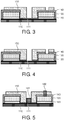
- Figure 1 schematically shows in its upper part a section through an intermediate product that may serve as a starting point for the manufacturing method according to the first method.
- the lower part of the Figure shows a top view onto this product.
- the product comprises a flat substrate 110, e.g. a plate of glass or transparent plastic, with a transparent anode layer 111 on top of it (e.g. ITO).
- a transparent anode layer 111 on top of it (e.g. ITO).
- two localized stacks are disposed on the anode layer 111, said stacks comprising an organic electroluminescent layer 120 and a cathode layer 130 on top of this.
- the anode layer 111, the organic electroluminescent layer 120, and the cathode layer 130 constitute "functional units", here more particularly light emitting units LU1, LU2, LU3, that are arranged on the common substrate 110.
- the light emitting units LU1, LU2, LU3 can freely be shaped according to the requirements in their intended application.
- the shape of the light emitting units can for instance be realized by using masks or plasma etch process steps.
- TFE thin film encapsulation
- Figure 2 shows the first step in this respect, which is the deposition of an inorganic encapsulation layer 140 (a water diffusion barrier), e.g. SiN.
- the TFE might start with the deposition of an organic layer, followed by the depicted inorganic layer.
- an organic layer 150 e.g. a polymer with no or a low water content.
- a printing process can be used, e.g. ink jet printing or plotting, or a lithographic process, e.g. (UV-)light exposure and etching.
- the organic layer 150 can be used as a mask to structure the inorganic layer 140 below and to open contacts to the anode layer 111 and the cathode layer 130 during plasma etch process.
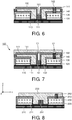
- Figure 5 shows the next (optional) process step, which is the application of conductive metal lines 161 and 162 as bus bars and/or contact lines, for example by printing or evaporation.
- Bus bars can be printed at the end of the manufacturing as well. They may have more elaborate shapes than contact lines, for example closed structures like a grid.
- Figure 6 shows the application of another inorganic layer 141 (e.g. a SiN layer), and Figure 7 the application of another organic layer 151 as a Topcoat printing. If needed, another SiN etch can follow to open contact points CT to the metal lines 161, 162, yielding the final OLED device 100.
- another SiN etch can follow to open contact points CT to the metal lines 161, 162, yielding the final OLED device 100.
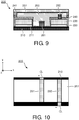
- an alternative OLED device 200 is shown in a sectional view ( Figures 8 , 9 ) and a top view ( Figure 10 ).
- This OLED device 200 comprises a structure for embedding metal contact lines and may be obtained by alternative processing steps following the stage of Figure 5 .
- the metal lines 261 and 262 may first be completely embedded (besides at lateral contact points CL) in an organic encapsulation layer 250, as illustrated in the sectional view of Figure 8 .
- This organic encapsulation layer 250 may then further be covered by an additional inorganic layer 241 and an additional organic layer 251.
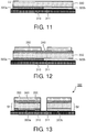
- Figures 11 to 13 illustrate steps of the inventive method that replace the steps of Figures 1 to 4 of the first method (not forming part of the invention).
- this embodiment starts with a substrate 310 having a (transparent) anode layer 311 and a light emitting unit LU on top.
- the light emitting unit LU is composed of two stripes 320a and 320b of different organic electroluminescent materials (e.g. emitting red and blue), carrying a cathode layer 330 on top. Of course more than two stripes (of different color) could be used as well.
- an unstructured inorganic layer 340 and a structured organic layer 350 are then deposited on the light emitting unit LU. This step is similar to what is shown in Figures 2 and 3 .
- the inorganic layer 340, the cathode layer 330, and the organic electroluminescent layers 320a, 320b have been etched, using the top organic layer 350 as a mask.
- several light emitting segments S1, S2 are generated on the substrate 310.
- further openings may be created in this way (not shown), too, particularly for providing access to the electrode layers.
- the further processing may proceed as illustrated in Figures 5 to 10 , i.e. by connecting the electrode layers to conductive lines and by encapsulating the segments S1, S2.
- a segmented OLED lighting tile 300 is provided.
- the invention can for instance be applied in OLED lighting, organic photovoltaics, or organic memories (MEMs).
- OLED lighting organic photovoltaics
- MEMs organic memories
Landscapes
- Physics & Mathematics (AREA)
- Electromagnetism (AREA)
- Optics & Photonics (AREA)
- Electroluminescent Light Sources (AREA)
Priority Applications (1)
| Application Number | Priority Date | Filing Date | Title |
|---|---|---|---|
| EP11773566.2A EP2628201B1 (en) | 2010-10-12 | 2011-10-06 | Method for manufacturing an organic electronic device with encapsulation |
Applications Claiming Priority (3)
| Application Number | Priority Date | Filing Date | Title |
|---|---|---|---|
| EP10187219 | 2010-10-12 | ||
| EP11773566.2A EP2628201B1 (en) | 2010-10-12 | 2011-10-06 | Method for manufacturing an organic electronic device with encapsulation |
| PCT/IB2011/054407 WO2012049594A1 (en) | 2010-10-12 | 2011-10-06 | Organic electronic device with encapsulation |
Publications (2)
| Publication Number | Publication Date |
|---|---|
| EP2628201A1 EP2628201A1 (en) | 2013-08-21 |
| EP2628201B1 true EP2628201B1 (en) | 2020-01-08 |
Family
ID=44860460
Family Applications (1)
| Application Number | Title | Priority Date | Filing Date |
|---|---|---|---|
| EP11773566.2A Active EP2628201B1 (en) | 2010-10-12 | 2011-10-06 | Method for manufacturing an organic electronic device with encapsulation |
Country Status (9)
| Country | Link |
|---|---|
| US (1) | US9219246B2 (enExample) |
| EP (1) | EP2628201B1 (enExample) |
| JP (1) | JP6014593B2 (enExample) |
| KR (1) | KR101843028B1 (enExample) |
| CN (1) | CN103155203B (enExample) |
| BR (1) | BR112013008571B1 (enExample) |
| RU (1) | RU2575938C2 (enExample) |
| TW (1) | TW201222914A (enExample) |
| WO (1) | WO2012049594A1 (enExample) |
Families Citing this family (13)
| Publication number | Priority date | Publication date | Assignee | Title |
|---|---|---|---|---|
| DE102012222772B4 (de) * | 2012-12-11 | 2021-09-16 | Pictiva Displays International Limited | Organisches optoelektronisches Bauelement |
| CN103904249B (zh) * | 2012-12-25 | 2016-05-18 | 海洋王照明科技股份有限公司 | 有机电致发光器件及其制备方法 |
| KR102088203B1 (ko) * | 2013-10-01 | 2020-03-12 | 엘지디스플레이 주식회사 | 유기발광 표시장치 및 이의 제조방법 |
| DE102014101518A1 (de) * | 2014-02-07 | 2015-08-13 | Osram Oled Gmbh | Organisches optoelektronisches Bauelement und Verfahren zum Herstellen eines organischen optoelektronischen Bauelements |
| FR3021460B1 (fr) * | 2014-05-26 | 2017-03-10 | Astron Fiamm Safety | Dispositif comprenant au moins deux diodes electroluminescentes organiques |
| CN104241330B (zh) | 2014-09-05 | 2017-05-03 | 京东方科技集团股份有限公司 | 有机发光二极管显示装置及其制作方法 |
| CN105206764A (zh) * | 2015-08-20 | 2015-12-30 | 深圳市星火辉煌系统工程有限公司 | 一种oled显示器件的密封工艺 |
| US9812667B2 (en) | 2015-11-04 | 2017-11-07 | Microsoft Technology Licensing, Llc | Patterning of OLED display stacks |
| CN109155373B (zh) * | 2016-04-12 | 2021-02-02 | 株式会社Lg化学 | 封装膜 |
| CN110911382B (zh) * | 2018-09-14 | 2021-06-25 | 群创光电股份有限公司 | 天线装置 |
| CN109904341B (zh) * | 2019-01-31 | 2020-08-04 | 武汉华星光电半导体显示技术有限公司 | 一种oled显示面板及其制备方法 |
| CN110323358B (zh) * | 2019-07-11 | 2021-12-24 | 京东方科技集团股份有限公司 | 发光二极管及其制造方法和发光装置 |
| CN110429064B (zh) * | 2019-08-01 | 2020-11-10 | 武汉华星光电半导体显示技术有限公司 | 缓冲结构、显示面板及缓冲结构的制作方法 |
Citations (1)
| Publication number | Priority date | Publication date | Assignee | Title |
|---|---|---|---|---|
| JP2007080569A (ja) * | 2005-09-12 | 2007-03-29 | Toyota Industries Corp | 有機エレクトロルミネッセンス素子の製造方法 |
Family Cites Families (19)
| Publication number | Priority date | Publication date | Assignee | Title |
|---|---|---|---|---|
| JP3537591B2 (ja) * | 1996-04-26 | 2004-06-14 | パイオニア株式会社 | 有機elディスプレイの製造方法 |
| US6274887B1 (en) * | 1998-11-02 | 2001-08-14 | Semiconductor Energy Laboratory Co., Ltd. | Semiconductor device and manufacturing method therefor |
| US6268695B1 (en) * | 1998-12-16 | 2001-07-31 | Battelle Memorial Institute | Environmental barrier material for organic light emitting device and method of making |
| BE1012802A3 (fr) * | 1999-07-28 | 2001-03-06 | Cockerill Rech & Dev | Dispositif electroluminescent et son procede de fabrication. |
| TW546857B (en) * | 2001-07-03 | 2003-08-11 | Semiconductor Energy Lab | Light-emitting device, method of manufacturing a light-emitting device, and electronic equipment |
| JP3761843B2 (ja) * | 2001-07-03 | 2006-03-29 | 株式会社半導体エネルギー研究所 | 発光装置及び電子機器 |
| JP3775499B2 (ja) * | 2002-01-08 | 2006-05-17 | 株式会社リコー | 半導体装置及びその製造方法、並びにdc−dcコンバータ |
| JP2004014447A (ja) * | 2002-06-11 | 2004-01-15 | Sony Corp | 表示装置およびその製造方法 |
| JP2006502537A (ja) * | 2002-10-07 | 2006-01-19 | コーニンクレッカ フィリップス エレクトロニクス エヌ ヴィ | 発光ディスプレイの製造方法 |
| WO2004032573A1 (en) * | 2002-10-07 | 2004-04-15 | Koninklijke Philips Electronics N.V. | Method for manufacturing a light emitting display |
| JP2005266616A (ja) * | 2004-03-19 | 2005-09-29 | Hideki Matsumura | 光学的表示装置及びその製造方法 |
| JP4708360B2 (ja) * | 2004-10-29 | 2011-06-22 | パイオニア株式会社 | 有機エレクトロルミネセンス表示装置及びその製造方法 |
| JP4696796B2 (ja) * | 2005-09-07 | 2011-06-08 | 株式会社豊田自動織機 | 有機エレクトロルミネッセンス素子の製造方法 |
| JP4795779B2 (ja) * | 2005-11-09 | 2011-10-19 | 株式会社アルバック | 有機エレクトロルミネッセンス表示パネル |
| US8003999B2 (en) * | 2005-12-30 | 2011-08-23 | Samsung Mobile Display Co., Ltd. | Organic light emitting device |
| JP2008071561A (ja) * | 2006-09-13 | 2008-03-27 | Fuji Electric Holdings Co Ltd | 有機el素子、および、有機el素子の製造方法 |
| JP2008270018A (ja) * | 2007-04-23 | 2008-11-06 | Toyota Industries Corp | 有機素子封止パネルの製造方法 |
| EP2144290A1 (en) * | 2008-07-08 | 2010-01-13 | Nederlandse Organisatie voor toegepast- natuurwetenschappelijk onderzoek TNO | Electronic device and method of manufacturing the same |
| FR2936651B1 (fr) * | 2008-09-30 | 2011-04-08 | Commissariat Energie Atomique | Dispositif optoelectronique organique et son procede d'encapsulation. |
-
2011
- 2011-10-06 WO PCT/IB2011/054407 patent/WO2012049594A1/en not_active Ceased
- 2011-10-06 KR KR1020137012212A patent/KR101843028B1/ko active Active
- 2011-10-06 RU RU2013121673/28A patent/RU2575938C2/ru active
- 2011-10-06 EP EP11773566.2A patent/EP2628201B1/en active Active
- 2011-10-06 BR BR112013008571-1A patent/BR112013008571B1/pt active IP Right Grant
- 2011-10-06 US US13/877,689 patent/US9219246B2/en active Active
- 2011-10-06 JP JP2013533301A patent/JP6014593B2/ja active Active
- 2011-10-06 CN CN201180049430.7A patent/CN103155203B/zh active Active
- 2011-10-11 TW TW100136809A patent/TW201222914A/zh unknown
Patent Citations (1)
| Publication number | Priority date | Publication date | Assignee | Title |
|---|---|---|---|---|
| JP2007080569A (ja) * | 2005-09-12 | 2007-03-29 | Toyota Industries Corp | 有機エレクトロルミネッセンス素子の製造方法 |
Also Published As
| Publication number | Publication date |
|---|---|
| JP6014593B2 (ja) | 2016-10-25 |
| BR112013008571A2 (pt) | 2019-11-19 |
| BR112013008571B1 (pt) | 2021-02-23 |
| KR101843028B1 (ko) | 2018-05-14 |
| CN103155203A (zh) | 2013-06-12 |
| JP2013542569A (ja) | 2013-11-21 |
| RU2575938C2 (ru) | 2016-02-27 |
| RU2013121673A (ru) | 2014-11-20 |
| CN103155203B (zh) | 2017-04-05 |
| EP2628201A1 (en) | 2013-08-21 |
| KR20130108388A (ko) | 2013-10-02 |
| US9219246B2 (en) | 2015-12-22 |
| TW201222914A (en) | 2012-06-01 |
| WO2012049594A1 (en) | 2012-04-19 |
| US20130217168A1 (en) | 2013-08-22 |
Similar Documents
| Publication | Publication Date | Title |
|---|---|---|
| EP2628201B1 (en) | Method for manufacturing an organic electronic device with encapsulation | |
| US20250241140A1 (en) | Organic electroluminescent devices | |
| JP7203763B2 (ja) | 表示基板及びその製造方法、表示装置 | |
| US12349588B2 (en) | OLED edge reinforcement holes and forming method | |
| EP3190624B1 (en) | Display panel, manufacturing method thereof, and display device | |
| EP2460205B1 (en) | Encapsulated optoelectronic device and method for making the same | |
| TWI581420B (zh) | 有機發光顯示設備及其製造方法 | |
| CN113838994B (zh) | 显示面板、柔性显示屏和电子设备及显示面板的制备方法 | |
| KR20160013244A (ko) | 유기 전계 발광 표시장치 및 유기 전계 발광 표시장치의 제조방법 | |
| CN103098215B (zh) | 有机电致发光器件 | |
| EP3428990B1 (en) | Lighting panel and method of fabricating the same | |
| KR20160038367A (ko) | 유기 발광 표시 장치 및 그 제조 방법 | |
| CN104737291A (zh) | 用于制造光电子组件的方法和光电子组件 | |
| EP2202819A1 (en) | Electro-optic device and method for manufacturing the same | |
| JP2007179914A (ja) | El装置及びその製造方法 | |
| KR20160005959A (ko) | 유기 발광 표시 장치 및 그 제조 방법 | |
| KR101032950B1 (ko) | 유기 전계 발광 소자의 제조방법 | |
| WO2011161610A2 (en) | Optoelectronic device with vertical connections |
Legal Events
| Date | Code | Title | Description |
|---|---|---|---|
| PUAI | Public reference made under article 153(3) epc to a published international application that has entered the european phase |
Free format text: ORIGINAL CODE: 0009012 |
|
| 17P | Request for examination filed |
Effective date: 20130513 |
|
| AK | Designated contracting states |
Kind code of ref document: A1 Designated state(s): AL AT BE BG CH CY CZ DE DK EE ES FI FR GB GR HR HU IE IS IT LI LT LU LV MC MK MT NL NO PL PT RO RS SE SI SK SM TR |
|
| RAP1 | Party data changed (applicant data changed or rights of an application transferred) |
Owner name: KONINKLIJKE PHILIPS N.V. Owner name: PHILIPS INTELLECTUAL PROPERTY & STANDARDS GMBH |
|
| DAX | Request for extension of the european patent (deleted) | ||
| STAA | Information on the status of an ep patent application or granted ep patent |
Free format text: STATUS: EXAMINATION IS IN PROGRESS |
|
| 17Q | First examination report despatched |
Effective date: 20171204 |
|
| RAP1 | Party data changed (applicant data changed or rights of an application transferred) |
Owner name: BEIJING XIAOMI MOBILE SOFTWARE CO., LTD. |
|
| GRAP | Despatch of communication of intention to grant a patent |
Free format text: ORIGINAL CODE: EPIDOSNIGR1 |
|
| STAA | Information on the status of an ep patent application or granted ep patent |
Free format text: STATUS: GRANT OF PATENT IS INTENDED |
|
| INTG | Intention to grant announced |
Effective date: 20190731 |
|
| GRAS | Grant fee paid |
Free format text: ORIGINAL CODE: EPIDOSNIGR3 |
|
| GRAA | (expected) grant |
Free format text: ORIGINAL CODE: 0009210 |
|
| STAA | Information on the status of an ep patent application or granted ep patent |
Free format text: STATUS: THE PATENT HAS BEEN GRANTED |
|
| AK | Designated contracting states |
Kind code of ref document: B1 Designated state(s): AL AT BE BG CH CY CZ DE DK EE ES FI FR GB GR HR HU IE IS IT LI LT LU LV MC MK MT NL NO PL PT RO RS SE SI SK SM TR |
|
| REG | Reference to a national code |
Ref country code: GB Ref legal event code: FG4D |
|
| REG | Reference to a national code |
Ref country code: CH Ref legal event code: EP |
|
| REG | Reference to a national code |
Ref country code: DE Ref legal event code: R096 Ref document number: 602011064512 Country of ref document: DE |
|
| REG | Reference to a national code |
Ref country code: IE Ref legal event code: FG4D |
|
| REG | Reference to a national code |
Ref country code: AT Ref legal event code: REF Ref document number: 1223795 Country of ref document: AT Kind code of ref document: T Effective date: 20200215 |
|
| REG | Reference to a national code |
Ref country code: NL Ref legal event code: MP Effective date: 20200108 |
|
| REG | Reference to a national code |
Ref country code: LT Ref legal event code: MG4D |
|
| PG25 | Lapsed in a contracting state [announced via postgrant information from national office to epo] |
Ref country code: FI Free format text: LAPSE BECAUSE OF FAILURE TO SUBMIT A TRANSLATION OF THE DESCRIPTION OR TO PAY THE FEE WITHIN THE PRESCRIBED TIME-LIMIT Effective date: 20200108 Ref country code: PT Free format text: LAPSE BECAUSE OF FAILURE TO SUBMIT A TRANSLATION OF THE DESCRIPTION OR TO PAY THE FEE WITHIN THE PRESCRIBED TIME-LIMIT Effective date: 20200531 Ref country code: NL Free format text: LAPSE BECAUSE OF FAILURE TO SUBMIT A TRANSLATION OF THE DESCRIPTION OR TO PAY THE FEE WITHIN THE PRESCRIBED TIME-LIMIT Effective date: 20200108 Ref country code: RS Free format text: LAPSE BECAUSE OF FAILURE TO SUBMIT A TRANSLATION OF THE DESCRIPTION OR TO PAY THE FEE WITHIN THE PRESCRIBED TIME-LIMIT Effective date: 20200108 Ref country code: LT Free format text: LAPSE BECAUSE OF FAILURE TO SUBMIT A TRANSLATION OF THE DESCRIPTION OR TO PAY THE FEE WITHIN THE PRESCRIBED TIME-LIMIT Effective date: 20200108 Ref country code: NO Free format text: LAPSE BECAUSE OF FAILURE TO SUBMIT A TRANSLATION OF THE DESCRIPTION OR TO PAY THE FEE WITHIN THE PRESCRIBED TIME-LIMIT Effective date: 20200408 |
|
| PG25 | Lapsed in a contracting state [announced via postgrant information from national office to epo] |
Ref country code: IS Free format text: LAPSE BECAUSE OF FAILURE TO SUBMIT A TRANSLATION OF THE DESCRIPTION OR TO PAY THE FEE WITHIN THE PRESCRIBED TIME-LIMIT Effective date: 20200508 Ref country code: BG Free format text: LAPSE BECAUSE OF FAILURE TO SUBMIT A TRANSLATION OF THE DESCRIPTION OR TO PAY THE FEE WITHIN THE PRESCRIBED TIME-LIMIT Effective date: 20200408 Ref country code: LV Free format text: LAPSE BECAUSE OF FAILURE TO SUBMIT A TRANSLATION OF THE DESCRIPTION OR TO PAY THE FEE WITHIN THE PRESCRIBED TIME-LIMIT Effective date: 20200108 Ref country code: SE Free format text: LAPSE BECAUSE OF FAILURE TO SUBMIT A TRANSLATION OF THE DESCRIPTION OR TO PAY THE FEE WITHIN THE PRESCRIBED TIME-LIMIT Effective date: 20200108 Ref country code: GR Free format text: LAPSE BECAUSE OF FAILURE TO SUBMIT A TRANSLATION OF THE DESCRIPTION OR TO PAY THE FEE WITHIN THE PRESCRIBED TIME-LIMIT Effective date: 20200409 Ref country code: HR Free format text: LAPSE BECAUSE OF FAILURE TO SUBMIT A TRANSLATION OF THE DESCRIPTION OR TO PAY THE FEE WITHIN THE PRESCRIBED TIME-LIMIT Effective date: 20200108 |
|
| REG | Reference to a national code |
Ref country code: DE Ref legal event code: R097 Ref document number: 602011064512 Country of ref document: DE |
|
| PG25 | Lapsed in a contracting state [announced via postgrant information from national office to epo] |
Ref country code: ES Free format text: LAPSE BECAUSE OF FAILURE TO SUBMIT A TRANSLATION OF THE DESCRIPTION OR TO PAY THE FEE WITHIN THE PRESCRIBED TIME-LIMIT Effective date: 20200108 Ref country code: DK Free format text: LAPSE BECAUSE OF FAILURE TO SUBMIT A TRANSLATION OF THE DESCRIPTION OR TO PAY THE FEE WITHIN THE PRESCRIBED TIME-LIMIT Effective date: 20200108 Ref country code: SK Free format text: LAPSE BECAUSE OF FAILURE TO SUBMIT A TRANSLATION OF THE DESCRIPTION OR TO PAY THE FEE WITHIN THE PRESCRIBED TIME-LIMIT Effective date: 20200108 Ref country code: EE Free format text: LAPSE BECAUSE OF FAILURE TO SUBMIT A TRANSLATION OF THE DESCRIPTION OR TO PAY THE FEE WITHIN THE PRESCRIBED TIME-LIMIT Effective date: 20200108 Ref country code: SM Free format text: LAPSE BECAUSE OF FAILURE TO SUBMIT A TRANSLATION OF THE DESCRIPTION OR TO PAY THE FEE WITHIN THE PRESCRIBED TIME-LIMIT Effective date: 20200108 Ref country code: RO Free format text: LAPSE BECAUSE OF FAILURE TO SUBMIT A TRANSLATION OF THE DESCRIPTION OR TO PAY THE FEE WITHIN THE PRESCRIBED TIME-LIMIT Effective date: 20200108 Ref country code: CZ Free format text: LAPSE BECAUSE OF FAILURE TO SUBMIT A TRANSLATION OF THE DESCRIPTION OR TO PAY THE FEE WITHIN THE PRESCRIBED TIME-LIMIT Effective date: 20200108 |
|
| PLBE | No opposition filed within time limit |
Free format text: ORIGINAL CODE: 0009261 |
|
| STAA | Information on the status of an ep patent application or granted ep patent |
Free format text: STATUS: NO OPPOSITION FILED WITHIN TIME LIMIT |
|
| REG | Reference to a national code |
Ref country code: AT Ref legal event code: MK05 Ref document number: 1223795 Country of ref document: AT Kind code of ref document: T Effective date: 20200108 |
|
| 26N | No opposition filed |
Effective date: 20201009 |
|
| PG25 | Lapsed in a contracting state [announced via postgrant information from national office to epo] |
Ref country code: IT Free format text: LAPSE BECAUSE OF FAILURE TO SUBMIT A TRANSLATION OF THE DESCRIPTION OR TO PAY THE FEE WITHIN THE PRESCRIBED TIME-LIMIT Effective date: 20200108 Ref country code: AT Free format text: LAPSE BECAUSE OF FAILURE TO SUBMIT A TRANSLATION OF THE DESCRIPTION OR TO PAY THE FEE WITHIN THE PRESCRIBED TIME-LIMIT Effective date: 20200108 |
|
| PG25 | Lapsed in a contracting state [announced via postgrant information from national office to epo] |
Ref country code: SI Free format text: LAPSE BECAUSE OF FAILURE TO SUBMIT A TRANSLATION OF THE DESCRIPTION OR TO PAY THE FEE WITHIN THE PRESCRIBED TIME-LIMIT Effective date: 20200108 Ref country code: PL Free format text: LAPSE BECAUSE OF FAILURE TO SUBMIT A TRANSLATION OF THE DESCRIPTION OR TO PAY THE FEE WITHIN THE PRESCRIBED TIME-LIMIT Effective date: 20200108 |
|
| REG | Reference to a national code |
Ref country code: CH Ref legal event code: PL |
|
| GBPC | Gb: european patent ceased through non-payment of renewal fee |
Effective date: 20201006 |
|
| PG25 | Lapsed in a contracting state [announced via postgrant information from national office to epo] |
Ref country code: LU Free format text: LAPSE BECAUSE OF NON-PAYMENT OF DUE FEES Effective date: 20201006 Ref country code: MC Free format text: LAPSE BECAUSE OF FAILURE TO SUBMIT A TRANSLATION OF THE DESCRIPTION OR TO PAY THE FEE WITHIN THE PRESCRIBED TIME-LIMIT Effective date: 20200108 |
|
| REG | Reference to a national code |
Ref country code: BE Ref legal event code: MM Effective date: 20201031 |
|
| PG25 | Lapsed in a contracting state [announced via postgrant information from national office to epo] |
Ref country code: FR Free format text: LAPSE BECAUSE OF NON-PAYMENT OF DUE FEES Effective date: 20201031 |
|
| PG25 | Lapsed in a contracting state [announced via postgrant information from national office to epo] |
Ref country code: BE Free format text: LAPSE BECAUSE OF NON-PAYMENT OF DUE FEES Effective date: 20201031 Ref country code: CH Free format text: LAPSE BECAUSE OF NON-PAYMENT OF DUE FEES Effective date: 20201031 Ref country code: LI Free format text: LAPSE BECAUSE OF NON-PAYMENT OF DUE FEES Effective date: 20201031 Ref country code: GB Free format text: LAPSE BECAUSE OF NON-PAYMENT OF DUE FEES Effective date: 20201006 |
|
| PG25 | Lapsed in a contracting state [announced via postgrant information from national office to epo] |
Ref country code: IE Free format text: LAPSE BECAUSE OF NON-PAYMENT OF DUE FEES Effective date: 20201006 |
|
| PG25 | Lapsed in a contracting state [announced via postgrant information from national office to epo] |
Ref country code: TR Free format text: LAPSE BECAUSE OF FAILURE TO SUBMIT A TRANSLATION OF THE DESCRIPTION OR TO PAY THE FEE WITHIN THE PRESCRIBED TIME-LIMIT Effective date: 20200108 Ref country code: MT Free format text: LAPSE BECAUSE OF FAILURE TO SUBMIT A TRANSLATION OF THE DESCRIPTION OR TO PAY THE FEE WITHIN THE PRESCRIBED TIME-LIMIT Effective date: 20200108 Ref country code: CY Free format text: LAPSE BECAUSE OF FAILURE TO SUBMIT A TRANSLATION OF THE DESCRIPTION OR TO PAY THE FEE WITHIN THE PRESCRIBED TIME-LIMIT Effective date: 20200108 |
|
| PG25 | Lapsed in a contracting state [announced via postgrant information from national office to epo] |
Ref country code: MK Free format text: LAPSE BECAUSE OF FAILURE TO SUBMIT A TRANSLATION OF THE DESCRIPTION OR TO PAY THE FEE WITHIN THE PRESCRIBED TIME-LIMIT Effective date: 20200108 Ref country code: AL Free format text: LAPSE BECAUSE OF FAILURE TO SUBMIT A TRANSLATION OF THE DESCRIPTION OR TO PAY THE FEE WITHIN THE PRESCRIBED TIME-LIMIT Effective date: 20200108 |
|
| REG | Reference to a national code |
Ref country code: DE Ref legal event code: R079 Ref document number: 602011064512 Country of ref document: DE Free format text: PREVIOUS MAIN CLASS: H01L0051520000 Ipc: H10K0050800000 |
|
| P01 | Opt-out of the competence of the unified patent court (upc) registered |
Effective date: 20230523 |
|
| PGFP | Annual fee paid to national office [announced via postgrant information from national office to epo] |
Ref country code: DE Payment date: 20241021 Year of fee payment: 14 |