EP2607947A2 - Anzeigevorrichtung mit elektromagnetischer Wellenabschirmstruktur - Google Patents
Anzeigevorrichtung mit elektromagnetischer Wellenabschirmstruktur Download PDFInfo
- Publication number
- EP2607947A2 EP2607947A2 EP12197814.2A EP12197814A EP2607947A2 EP 2607947 A2 EP2607947 A2 EP 2607947A2 EP 12197814 A EP12197814 A EP 12197814A EP 2607947 A2 EP2607947 A2 EP 2607947A2
- Authority
- EP
- European Patent Office
- Prior art keywords
- electromagnetic wave
- rear case
- display apparatus
- circuit board
- printed circuit
- Prior art date
- Legal status (The legal status is an assumption and is not a legal conclusion. Google has not performed a legal analysis and makes no representation as to the accuracy of the status listed.)
- Withdrawn
Links
Images


Classifications
-
- H—ELECTRICITY
- H05—ELECTRIC TECHNIQUES NOT OTHERWISE PROVIDED FOR
- H05K—PRINTED CIRCUITS; CASINGS OR CONSTRUCTIONAL DETAILS OF ELECTRIC APPARATUS; MANUFACTURE OF ASSEMBLAGES OF ELECTRICAL COMPONENTS
- H05K9/00—Screening of apparatus or components against electric or magnetic fields
-
- G—PHYSICS
- G02—OPTICS
- G02F—OPTICAL DEVICES OR ARRANGEMENTS FOR THE CONTROL OF LIGHT BY MODIFICATION OF THE OPTICAL PROPERTIES OF THE MEDIA OF THE ELEMENTS INVOLVED THEREIN; NON-LINEAR OPTICS; FREQUENCY-CHANGING OF LIGHT; OPTICAL LOGIC ELEMENTS; OPTICAL ANALOGUE/DIGITAL CONVERTERS
- G02F1/00—Devices or arrangements for the control of the intensity, colour, phase, polarisation or direction of light arriving from an independent light source, e.g. switching, gating or modulating; Non-linear optics
- G02F1/01—Devices or arrangements for the control of the intensity, colour, phase, polarisation or direction of light arriving from an independent light source, e.g. switching, gating or modulating; Non-linear optics for the control of the intensity, phase, polarisation or colour
- G02F1/13—Devices or arrangements for the control of the intensity, colour, phase, polarisation or direction of light arriving from an independent light source, e.g. switching, gating or modulating; Non-linear optics for the control of the intensity, phase, polarisation or colour based on liquid crystals, e.g. single liquid crystal display cells
- G02F1/133—Constructional arrangements; Operation of liquid crystal cells; Circuit arrangements
- G02F1/1333—Constructional arrangements; Manufacturing methods
- G02F1/133308—Support structures for LCD panels, e.g. frames or bezels
-
- G—PHYSICS
- G09—EDUCATION; CRYPTOGRAPHY; DISPLAY; ADVERTISING; SEALS
- G09F—DISPLAYING; ADVERTISING; SIGNS; LABELS OR NAME-PLATES; SEALS
- G09F9/00—Indicating arrangements for variable information in which the information is built-up on a support by selection or combination of individual elements
-
- G—PHYSICS
- G02—OPTICS
- G02F—OPTICAL DEVICES OR ARRANGEMENTS FOR THE CONTROL OF LIGHT BY MODIFICATION OF THE OPTICAL PROPERTIES OF THE MEDIA OF THE ELEMENTS INVOLVED THEREIN; NON-LINEAR OPTICS; FREQUENCY-CHANGING OF LIGHT; OPTICAL LOGIC ELEMENTS; OPTICAL ANALOGUE/DIGITAL CONVERTERS
- G02F1/00—Devices or arrangements for the control of the intensity, colour, phase, polarisation or direction of light arriving from an independent light source, e.g. switching, gating or modulating; Non-linear optics
- G02F1/01—Devices or arrangements for the control of the intensity, colour, phase, polarisation or direction of light arriving from an independent light source, e.g. switching, gating or modulating; Non-linear optics for the control of the intensity, phase, polarisation or colour
- G02F1/13—Devices or arrangements for the control of the intensity, colour, phase, polarisation or direction of light arriving from an independent light source, e.g. switching, gating or modulating; Non-linear optics for the control of the intensity, phase, polarisation or colour based on liquid crystals, e.g. single liquid crystal display cells
- G02F1/133—Constructional arrangements; Operation of liquid crystal cells; Circuit arrangements
- G02F1/1333—Constructional arrangements; Manufacturing methods
- G02F1/133308—Support structures for LCD panels, e.g. frames or bezels
- G02F1/133314—Back frames
-
- G—PHYSICS
- G02—OPTICS
- G02F—OPTICAL DEVICES OR ARRANGEMENTS FOR THE CONTROL OF LIGHT BY MODIFICATION OF THE OPTICAL PROPERTIES OF THE MEDIA OF THE ELEMENTS INVOLVED THEREIN; NON-LINEAR OPTICS; FREQUENCY-CHANGING OF LIGHT; OPTICAL LOGIC ELEMENTS; OPTICAL ANALOGUE/DIGITAL CONVERTERS
- G02F1/00—Devices or arrangements for the control of the intensity, colour, phase, polarisation or direction of light arriving from an independent light source, e.g. switching, gating or modulating; Non-linear optics
- G02F1/01—Devices or arrangements for the control of the intensity, colour, phase, polarisation or direction of light arriving from an independent light source, e.g. switching, gating or modulating; Non-linear optics for the control of the intensity, phase, polarisation or colour
- G02F1/13—Devices or arrangements for the control of the intensity, colour, phase, polarisation or direction of light arriving from an independent light source, e.g. switching, gating or modulating; Non-linear optics for the control of the intensity, phase, polarisation or colour based on liquid crystals, e.g. single liquid crystal display cells
- G02F1/133—Constructional arrangements; Operation of liquid crystal cells; Circuit arrangements
- G02F1/1333—Constructional arrangements; Manufacturing methods
- G02F1/133308—Support structures for LCD panels, e.g. frames or bezels
- G02F1/133334—Electromagnetic shields
-
- G—PHYSICS
- G02—OPTICS
- G02F—OPTICAL DEVICES OR ARRANGEMENTS FOR THE CONTROL OF LIGHT BY MODIFICATION OF THE OPTICAL PROPERTIES OF THE MEDIA OF THE ELEMENTS INVOLVED THEREIN; NON-LINEAR OPTICS; FREQUENCY-CHANGING OF LIGHT; OPTICAL LOGIC ELEMENTS; OPTICAL ANALOGUE/DIGITAL CONVERTERS
- G02F2201/00—Constructional arrangements not provided for in groups G02F1/00 - G02F7/00
- G02F2201/50—Protective arrangements
- G02F2201/503—Arrangements improving the resistance to shock
Definitions
- Exemplary embodiments of the inventive concept relate to a display apparatus having an electromagnetic wave shielding structure which is capable of shielding an electromagnetic wave generated inside the display apparatus.
- a display apparatus is an apparatus which is configured to display an image on a surface of a display panel in a visual manner, and is provided with various electronic components such as circuit elements mounted thereon in order to drive the display apparatus.
- an electromagnetic wave is generated at the electronic components which are inside the display apparatus.
- the electromagnetic wave causes electromagnetic interference (EMI) to occur at the electronic components which are inside the display apparatus.
- EMI electromagnetic interference
- the electromagnetic wave generated inside the display apparatus is emitted outside the display apparatus without being shielded
- the electromagnetic wave may cause electromagnetic interference with other electronic apparatuses, and the electromagnetic wave emitted to the outside of the display apparatus may affect the body of a user.
- the display apparatus uses various exterior trims as the display apparatus is further formed with a compact structure.
- a display apparatus includes a display panel, a rear case, a printed circuit board, an electromagnetic wave reducer.
- the rear case may be disposed at a rear of the display panel and formed of a non-conductive material.
- the printed circuit board may be disposed at a rear of the rear case.
- the electromagnetic wave reducer may be provided at one surface of the rear case and may be formed of a conductive material in order to reduce the electromagnetic wave generated at the printed circuit board.
- the electromagnetic wave reducer may be electrically connected to the printed circuit board.
- the display apparatus may further include at least one first connecting apparatus which is configured to electrically connect the printed circuit board to the electromagnetic wave reducing member.
- the first connecting apparatus may include a first stud, which is installed at the rear case and is configured to be electrically connected to the electromagnetic wave reducer, and a coupling member which is coupled between the printed circuit board and the first stud.
- the rear case may be formed with glass material.
- the electromagnetic wave reducer may be formed with a metallic layer.
- An anti-scattering film may be attached to a surface of the electromagnetic wave reducer in order to prevent scattering of debris from the rear case in a situation where the rear case is damaged.
- the electromagnetic wave reducer may be formed with an electromagnetic interference (EMI) sheet, and may be attached to the rear case.
- EMI electromagnetic interference
- the electromagnetic wave reducer may be attached to a portion of one surface of the rear case, and a film, which is configured to prevent debris from being scattered in a situation where the rear case is damaged, is attached to at least one area of the remaining portion of the one surface of the rear case, the remaining portion to which the electromagnetic wave reducer is not attached.
- the display apparatus may further include a cover which is disposed at a rear of the printed circuit board in order to protect the printed circuit board.
- the electromagnetic wave reducer may be electrically connected to the cover.
- the display apparatus may further include at least one second connecting apparatus which is configured to electrically connect the cover to the electromagnetic wave reducer.
- the second connecting apparatus may include a second stud, which is installed at the rear case and electrically connected to the electromagnetic wave reducer, and a coupling member which is coupled between the cover and the second stud.
- a display apparatus includes a display panel, a rear case, a printed circuit board, a cover and a conductive material.
- the rear case may be formed of a non-conductive material, and may be disposed at a rear portion of the display panel.
- the printed circuit board may be disposed at a rear portion of the rear case.
- the cover may be disposed at a rear portion of the printed circuit board in order to protect the printed circuit board.
- the conductive material may be provided at one surface of the rear case. The conductive material may be electrically connected to the cover and to the printed circuit board.
- the display apparatus may further include a first connecting apparatus that may be configured to secure the printed circuit board to the rear case while electrically connecting the printed circuit board to the conductive material.
- the display apparatus may further include a second connecting apparatus that may be configured to secure the cover to the rear case while electrically connecting the cover to the conductive material.
- the conductive material may be a metallic layer formed at one surface of the rear case.
- the rear case may be formed with glass material.
- An exemplary embodiment may include a display apparatus, including: a rear case; a printed circuit board disposed at a rear portion of a rear case, and an electromagnetic wave reducer provided at one surface of the rear case and formed of a conductive material to reduce electromagnetic waves generated at the printed circuit board.
- An anti-scattering film may be attached to a surface of the electromagnetic wave reducer. In response to the rear case being damaged, the anti-scattering film may prevent debris of the rear case from being scattered.
- the electromagnetic wave reducer may be attached to the rear case and may be formed with an electromagnetic interference (EMI) sheet.
- EMI electromagnetic interference
- the electromagnetic wave reducer may be attached to a portion of one surface of the rear case, and a film may be attached to at least one area of the remaining portion of the one surface of the rear case to which the electromagnetic wave reducer is not attached.
- the film may be configured to prevent debris from being scattered in a situation where the rear case is damaged.
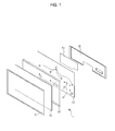
- a display apparatus 1 includes a display module 20 which displays an image; cases 10, 30, and 40 which form an exterior appearance of the display apparatus 1 while covering the display apparatus 1; a printed circuit board 50 which drives the display module 20, and a cover 60 which protects the printed circuit board 50.
- the cases 10, 30, and 40 include a front case 10 disposed at an edge portion of the front surface of the display module 20, a rear case 40 disposed at a rear of the display module 20, and a middle case 30 having the display module 20 disposed at a periphery thereof and coupled between the front case 10 and the rear case 40.
- the rear case 40 which covers the entire rear surface of the display module 20, may be formed in a panel having a size which corresponds to the display module 20.
- the rear case 40 is provided with a plurality of penetrating holes 42 which allows various cables (not shown) configured to deliver an image signal and to supply power to the display module 20, to pass therethrough.
- the rear case 40 is provided with a plurality of installation holes 41 configured for the installation of the various components such as the printed circuit board 50 and the cover 60, which is disposed at a rear of the rear case 40.
- the rear case 40 may include an heat radiation sheet (not shown) which is configured to induce the heat generated at the display module 20 and the printed circuit board 50, to be radiated outside the rear case 40.
- the radiation sheet as such may be provided at entire one surface of the rear case 40, or at a portion of an area of the rear case 40.
- the printed circuit board 50 is provided with a predetermined circuit pattern formed thereon, and a plurality of circuit devices are installed on the circuit pattern.
- the cover 60 is disposed at a rear of the printed circuit board 50, and may be composed to cover an area at which electronic components, as well as the printed circuit board 50, such as a power supply, are installed.
- the front case 10 is installed at the front surface of the display module 20 to form a bezel.
- the middle case 30 may be formed in a way to finish the side surface portion between the display module 20 and the rear case 40.
- front case 10 and the middle case 30 may be integrally formed with each other to be composed as one case to finish the front surface and the side surface of the display module 20.
- the rear case 40 is disposed while being spaced apart from the display module 20, and may be formed with tempered glass or plastic resin, both of which are non-conductive material.
- an electromagnetic wave reducer 90 composed of non-conductive material is provided.
- the electromagnetic wave reducer 90 may be a metallic layer which is formed by depositing metal such as stainless steel, or may be formed of pre-processed metal foil or a metallic panel such as ion plate or copper plate.
- the electromagnetic wave reducer 90 as such may be provided at an entire area of the inner surface of the rear case 40, or may be provided at a portion of the inner surface of the rear case 40.
- the rear case 40 is composed of glass, and an anti-scattering film 91 is attached at an outer surface of the electromagnetic wave reducer 90 in preparation for a situation where the rear case 40 is damaged by a physical impact.
- the anti-scattering film 91 is configured to prevent the scattering of the debris by applying certain protection with respect to the debris, and furthermore, prevents the rear case 40 from being perforated so that the display module 20 located at an inner side of the rear case 40 is protected.
- the anti-scattering film 91 may be provided to cover an entire inner surface of the rear case 40.
- the anti-scattering film 91 may be directly attached at the inner surface of the rear case 40 with respect to an area of the inner surface of the rear case 40 at which the electromagnetic wave reducer 90 is not provided.
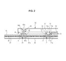
- a first connecting apparatus 70 is provided between the rear case 40 and the printed circuit board 50.
- the first connecting apparatus 70 is configured to support the printed circuit board 50 to have the printed circuit board 50 fixed while spaced apart from the rear case 40, and at the same time, is configured to electrically connect between the printed circuit board 50 and the electromagnetic wave reducer 90.
- the first connecting apparatus 70 may include a stud 71 installed at the rear case 40, and a coupling member 73 coupled between the printed circuit board 50 and the stud 71.
- the installation hole 41 is provided so that the stud 1 may be installed at the rear case 40, and at the installation hole 41, a reinforcing member 72 is installed to supplement the strength and the mechanical characteristic of the installation hole 41.
- the stud 71 is disposed at an inner side of the rear case 40, and includes flange 71a and a pillar 81b which are configured to penetrate an inner and an outer portion of the rear case 40 through the installation hole 41.
- the flange 71a in a state where stud 71 is installed at the installation hole 41, is configured to support the pillar 71b while forming the contact surface with the electromagnetic wave reducer 90, and enables the stud 71 to be electrically connected to the electromagnetic wave reducer 90.
- the coupling member 73 may be composed of a bolt having a head 73a and a screw 73b. While in a state of the coupling member 73 being installed, the head 73a is connected to a linker 52 while being coupled to a hole 51 of the printed circuit board 50, and also the screw 73b is coupled to a screw hole formed at the pillar 71b of the stud 71.
- the anti-scattering film 91 may be eliminated from an area between the flange 71a and the electromagnetic wave reducer 90 so that the flange 71a of the stud 71 may be connected to the electromagnetic wave reducer 90.
- the one first connecting apparatus 70 connects between the printed circuit board 50 and the rear case 40.
- the above is provided as one example of a connecting relationship between the printed circuit board 50 and the rear case 40;, and a plurality of first connecting apparatuses 70 may be installed between the printed circuit board 50 and the rear case 40.
- a second connecting apparatus 80 is installed between the cover 60 and the rear case 40.
- the second connecting apparatus 80 as a whole is composed in a similar manner to the first connecting apparatus 70, and may include a stud 81 installed at the rear case 40, and may include a coupling member 83 coupled between the cover 60 and the stud 81.
- the stud 81 to be compatible with the first connecting apparatus 70, may be formed similar to the stud 71 of the first connecting apparatus 70. However, in a situation where the coupling member 83, by considering that the distance up to the cover 60 disposed at a rear of the printed circuit board 50 from the rear case 40 is longer than the distance up to the printed circuit board 50 from the rear case 40, the length of the coupling member 83 is formed to be longer than the coupling member 73 of the first connecting apparatus 70.
- the installation hole 41 is provided so that the stud 81 may be installed at the rear case 40, and at the installation hole 41, a reinforcing member 82 is installed to supplement the strength and the mechanical characteristic of the installation hole 41.
- the installation hole 41 as such may be composed in a similar manner to the installation hole 41 that is configured for the installation of the first connecting apparatus 70.
- the stud 81 is disposed at an inner side of the rear case 40, and includes a flange 81a and a pillar 81b which are configured to penetrate an inner and an outer portion of the rear case 40 through the installation hole 41.
- the coupling member 83 may be composed of a bolt having a head 83a and a screw 83b In a state of the coupling member 83 being installed, the head 83a is connected to the cover 60 while being coupled to a hole of the cover 60, and also the screw 83b is coupled to a screw hole formed at the pillar 81b of the stud 81.
- the cover 60 is formed in a metallic panel, and is configured to block an electromagnetic wave from being discharged outside of the display apparatus 1, and at the same time, may form a grounding structure that is configured to induce the reduction of an electromagnetic wave.
- the anti-scattering film 91 may be eliminated from an area in between the flange 81a and the electromagnetic wave reducer 90 so that the flange 81a of the stud 81 may be connected to the electromagnetic wave reducer 90.
- the printed circuit board 50 is electrically connected, respectively, to each of the electromagnetic wave reducer 90 and the cover 60 through the first connecting apparatus 70 and the second connecting apparatus 80, a single circuit configured to reduce the electromagnetic wave being absorbed through the cover 60 and the electromagnetic wave reducing 90 is provided.
- FIGS. 3 to 4 a display apparatus in accordance with another exemplary embodiment of the inventive concept will be described.
- the electromagnetic wave reducer 90 is composed of an electromagnetic interference sheet (EMI).
- EMI electromagnetic interference sheet
- the EMI sheet is referred to as a sheet composed of fiber coated with metal having high electrical conductivity, and the description of the EMI sheet is already known. Thus, the detailed description of the EMI sheet will be omitted.
- the anti-scattering film 91 is attached to the entire inner surface of the rear case 40; and the EMI sheet is attached to an area, at which the shielding of the electromagnetic wave is determined to be needed, thereby forming the electromagnetic wave reducer 90.
- the anti-scattering film 91 is attached to the inner surface of the rear case 40, but the EMI sheet is attached without attaching the anti-scattering film 91 to an area at which the EMI sheet is to be attached. If the EMI sheet is attached to the rear case 40, the EMI sheet, similar to the anti-scattering film 91, may provide certain protection with respect to the debris in a situation where the rear case 40 is damaged. Thus, the anti-scattering film 91 may serve as the EMI sheet.
- the use of the anti-scattering film 91 may be reduced to the same extent as the area which corresponds to the area at which the EMI sheet is attached, thereby reducing the manufacturing cost of the display apparatus.
- FIG. 5 a display apparatus in accordance with another exemplary embodiment of the inventive concept will be described.
- the cover 60 may be composed of non-conductive material that is not metallic material.
- the cover 60 may be composed of glass.
- an electromagnetic wave reducer 95 is provided at an inner surface of the cover 60, similar to the rear case 40.
- the electromagnetic wave reducer 95 may be a metallic layer which are formed by depositing metal such as stainless steel, or may be formed of pre-processed metal foil or a metallic panel such as an ion plate or as a copper plate.
- an anti-scattering film 96 configured to prepare for the damage of the cover 60 may be attached on the electromagnetic wave reducer 95, and an installation hole 60a through which the coupling member 83 penetrates is provided at the cover 60.
- a reinforcing member 61 is installed to supplement the strength of the installation hole 60a, and the reinforcing member 61 electrically connects between the electromagnetic wave reducer 95 and the coupling member 83.
- the electromagnetic wave reducer 95 may be composed of the EMI sheet.
- the remaining area other than the area at which the EMI sheet is attached is provided with the anti-scattering film 96 being selectively attached thereto.
- the EMI sheet may be attached at the entire inner surface area of the cover 60, and the attachment of the anti-scattering film 96 may be omitted.
Landscapes
- Physics & Mathematics (AREA)
- Nonlinear Science (AREA)
- General Physics & Mathematics (AREA)
- Engineering & Computer Science (AREA)
- Mathematical Physics (AREA)
- Chemical & Material Sciences (AREA)
- Crystallography & Structural Chemistry (AREA)
- Optics & Photonics (AREA)
- Microelectronics & Electronic Packaging (AREA)
- Theoretical Computer Science (AREA)
- Shielding Devices Or Components To Electric Or Magnetic Fields (AREA)
- Devices For Indicating Variable Information By Combining Individual Elements (AREA)
Applications Claiming Priority (1)
| Application Number | Priority Date | Filing Date | Title |
|---|---|---|---|
| KR1020110140113A KR20130072608A (ko) | 2011-12-22 | 2011-12-22 | 디스플레이 장치 |
Publications (2)
| Publication Number | Publication Date |
|---|---|
| EP2607947A2 true EP2607947A2 (de) | 2013-06-26 |
| EP2607947A3 EP2607947A3 (de) | 2014-06-04 |
Family
ID=47602990
Family Applications (1)
| Application Number | Title | Priority Date | Filing Date |
|---|---|---|---|
| EP12197814.2A Withdrawn EP2607947A3 (de) | 2011-12-22 | 2012-12-18 | Anzeigevorrichtung mit elektromagnetischer Wellenabschirmstruktur |
Country Status (4)
| Country | Link |
|---|---|
| US (1) | US20130163214A1 (de) |
| EP (1) | EP2607947A3 (de) |
| KR (1) | KR20130072608A (de) |
| CN (1) | CN103177658A (de) |
Families Citing this family (6)
| Publication number | Priority date | Publication date | Assignee | Title |
|---|---|---|---|---|
| KR102094888B1 (ko) * | 2013-07-29 | 2020-03-30 | 엘지전자 주식회사 | 디스플레이 장치 |
| CN103442192A (zh) * | 2013-08-29 | 2013-12-11 | 惠州市颂誉玻璃有限公司 | 电视机玻璃背板 |
| JP6288278B2 (ja) * | 2014-08-12 | 2018-03-07 | 日産自動車株式会社 | 車両のコンソールボックスにおける電磁波遮蔽構造 |
| KR102219936B1 (ko) | 2018-08-23 | 2021-02-25 | 삼성전자주식회사 | 디스플레이 장치 |
| CN109917577B (zh) * | 2019-01-31 | 2021-10-22 | 南京巨鲨显示科技有限公司 | 一种抗电磁干扰的便携式显示器 |
| KR20240170196A (ko) * | 2023-05-26 | 2024-12-03 | 현대모비스 주식회사 | 디스플레이 장치 및 이를 장착한 차량 |
Family Cites Families (20)
| Publication number | Priority date | Publication date | Assignee | Title |
|---|---|---|---|---|
| JPS63253987A (ja) * | 1987-04-10 | 1988-10-20 | シャープ株式会社 | El表示装置の電磁シ−ルド構造 |
| US5597979A (en) * | 1995-05-12 | 1997-01-28 | Schlegel Corporation | EMI shielding having flexible condustive sheet and I/O Gasket |
| JPH09218649A (ja) * | 1996-02-09 | 1997-08-19 | Matsushita Electric Ind Co Ltd | 液晶表示装置及びそのシールド板 |
| JPH09269480A (ja) * | 1996-03-29 | 1997-10-14 | Sanyo Electric Co Ltd | 液晶表示装置 |
| JPH10282896A (ja) * | 1997-04-07 | 1998-10-23 | Mitsubishi Electric Corp | 表示装置 |
| US5953206A (en) * | 1997-10-15 | 1999-09-14 | Hewlett-Packard Company | Thermal dissipation and EMI shielding structure for notebook computers |
| JPH11191383A (ja) * | 1997-12-26 | 1999-07-13 | Matsushita Electron Corp | 平板状画像表示装置 |
| ATE269631T1 (de) * | 2000-01-22 | 2004-07-15 | Helmut Kahl | Verfahren zur herstellung einer elektromagnetischen abschirmung |
| KR20040008265A (ko) * | 2002-07-06 | 2004-01-31 | 엘지전자 주식회사 | 플라즈마 디스플레이 패널 |
| CN101031191A (zh) * | 2006-02-27 | 2007-09-05 | 明基电通股份有限公司 | 显示装置 |
| TWI342424B (en) * | 2006-11-27 | 2011-05-21 | Chimei Innolux Corp | Liquid crystal display device |
| KR101329280B1 (ko) * | 2006-12-11 | 2013-11-14 | 삼성디스플레이 주식회사 | 표시 장치 |
| CN100570406C (zh) * | 2007-04-27 | 2009-12-16 | 甘国工 | 液晶显示器用的安全玻璃保护屏及使用该屏的液晶显示器 |
| US7936567B2 (en) * | 2007-05-07 | 2011-05-03 | Ngk Spark Plug Co., Ltd. | Wiring board with built-in component and method for manufacturing the same |
| KR100911007B1 (ko) * | 2007-05-18 | 2009-08-05 | 삼성에스디아이 주식회사 | 샤시 베이스 조립체와, 이를 포함한 디스플레이 장치 |
| CN101365310A (zh) * | 2007-08-08 | 2009-02-11 | 佳世达科技股份有限公司 | 电路板结合于后壳的显示装置 |
| JP5138395B2 (ja) * | 2008-01-22 | 2013-02-06 | 新光電気工業株式会社 | 配線基板及びその製造方法 |
| JP2009231818A (ja) * | 2008-03-21 | 2009-10-08 | Ibiden Co Ltd | 多層プリント配線板及びその製造方法 |
| KR20100046594A (ko) * | 2008-10-27 | 2010-05-07 | 엘지전자 주식회사 | 휴대 단말기 |
| KR101580126B1 (ko) * | 2009-07-21 | 2015-12-28 | 엘지전자 주식회사 | 이동 단말기 |
-
2011
- 2011-12-22 KR KR1020110140113A patent/KR20130072608A/ko not_active Withdrawn
-
2012
- 2012-12-18 EP EP12197814.2A patent/EP2607947A3/de not_active Withdrawn
- 2012-12-21 CN CN2012105643997A patent/CN103177658A/zh active Pending
- 2012-12-21 US US13/724,281 patent/US20130163214A1/en not_active Abandoned
Non-Patent Citations (1)
| Title |
|---|
| None |
Also Published As
| Publication number | Publication date |
|---|---|
| CN103177658A (zh) | 2013-06-26 |
| US20130163214A1 (en) | 2013-06-27 |
| EP2607947A3 (de) | 2014-06-04 |
| KR20130072608A (ko) | 2013-07-02 |
Similar Documents
| Publication | Publication Date | Title |
|---|---|---|
| US20130163214A1 (en) | Display apparatus with an electromagnetic wave shielding structure | |
| JP6301056B2 (ja) | 電子機器 | |
| EP1418798B1 (de) | Leiterplatte und Methode um eine Leiterplatte an einem elektrisch leitenden Gehäuse anzubringen | |
| US20090086420A1 (en) | Rugged conductive housing structure for portable computing device display | |
| EP2793073A1 (de) | Anzeigevorrichtung | |
| US20080259542A1 (en) | Plasma display | |
| JP6453758B2 (ja) | 電気装置 | |
| CN103857267A (zh) | 电子设备的屏蔽结构 | |
| CN215872067U (zh) | 电子设备 | |
| JP2006032845A (ja) | 透明シールドケース及びその製造方法並びに遊技機 | |
| JP5949374B2 (ja) | 電子機器 | |
| CN106659102A (zh) | 一种强电磁脉冲屏蔽防护加固机箱 | |
| JP6094232B2 (ja) | 表示装置 | |
| US12495531B2 (en) | Electronic apparatus | |
| JP2018037661A (ja) | 電子機器 | |
| US20060081389A1 (en) | Aesthetically colored EMI shields | |
| US9323093B2 (en) | Method of suppressing electromagnetic interference radiation from a display device | |
| US9961810B2 (en) | Display device | |
| US20060080825A1 (en) | Methods related to electromagnetic interference shielding | |
| EP4467378B1 (de) | Anzeigevorrichtung und damit ausgestattetes fahrzeug | |
| JP2005205887A (ja) | デジタル電子機器 | |
| US20250081372A1 (en) | Display device and vehicle having the same | |
| TWI919213B (zh) | 電子裝置 | |
| EP1921905B1 (de) | Abschirmendes pinboard-modul | |
| CN203630680U (zh) | 电子设备构造 |
Legal Events
| Date | Code | Title | Description |
|---|---|---|---|
| AK | Designated contracting states |
Kind code of ref document: A2 Designated state(s): AL AT BE BG CH CY CZ DE DK EE ES FI FR GB GR HR HU IE IS IT LI LT LU LV MC MK MT NL NO PL PT RO RS SE SI SK SM TR |
|
| AX | Request for extension of the european patent |
Extension state: BA ME |
|
| PUAI | Public reference made under article 153(3) epc to a published international application that has entered the european phase |
Free format text: ORIGINAL CODE: 0009012 |
|
| PUAL | Search report despatched |
Free format text: ORIGINAL CODE: 0009013 |
|
| AK | Designated contracting states |
Kind code of ref document: A3 Designated state(s): AL AT BE BG CH CY CZ DE DK EE ES FI FR GB GR HR HU IE IS IT LI LT LU LV MC MK MT NL NO PL PT RO RS SE SI SK SM TR |
|
| AX | Request for extension of the european patent |
Extension state: BA ME |
|
| RIC1 | Information provided on ipc code assigned before grant |
Ipc: H05K 9/00 20060101ALI20140428BHEP Ipc: G02F 1/1333 20060101AFI20140428BHEP Ipc: H01J 11/44 20120101ALI20140428BHEP |
|
| 17P | Request for examination filed |
Effective date: 20141204 |
|
| RBV | Designated contracting states (corrected) |
Designated state(s): AL AT BE BG CH CY CZ DE DK EE ES FI FR GB GR HR HU IE IS IT LI LT LU LV MC MK MT NL NO PL PT RO RS SE SI SK SM TR |
|
| STAA | Information on the status of an ep patent application or granted ep patent |
Free format text: STATUS: REQUEST FOR EXAMINATION WAS MADE |
|
| STAA | Information on the status of an ep patent application or granted ep patent |
Free format text: STATUS: THE APPLICATION IS DEEMED TO BE WITHDRAWN |
|
| 18D | Application deemed to be withdrawn |
Effective date: 20170701 |