EP1921905B1 - Abschirmendes pinboard-modul - Google Patents
Abschirmendes pinboard-modul Download PDFInfo
- Publication number
- EP1921905B1 EP1921905B1 EP06742180A EP06742180A EP1921905B1 EP 1921905 B1 EP1921905 B1 EP 1921905B1 EP 06742180 A EP06742180 A EP 06742180A EP 06742180 A EP06742180 A EP 06742180A EP 1921905 B1 EP1921905 B1 EP 1921905B1
- Authority
- EP
- European Patent Office
- Prior art keywords
- shielding
- subrack
- backplane
- cover plate
- circuit board
- Prior art date
- Legal status (The legal status is an assumption and is not a legal conclusion. Google has not performed a legal analysis and makes no representation as to the accuracy of the status listed.)
- Not-in-force
Links
Images


Classifications
-
- H—ELECTRICITY
- H05—ELECTRIC TECHNIQUES NOT OTHERWISE PROVIDED FOR
- H05K—PRINTED CIRCUITS; CASINGS OR CONSTRUCTIONAL DETAILS OF ELECTRIC APPARATUS; MANUFACTURE OF ASSEMBLAGES OF ELECTRICAL COMPONENTS
- H05K9/00—Screening of apparatus or components against electric or magnetic fields
- H05K9/0062—Structures of standardised dimensions, e.g. 19" rack, chassis for servers or telecommunications
Definitions
- the present invention relates to a communication product, especially a shielding subrack module.
- Electromagnetic compatibility (EMC) Compulsory Certification relating to electronic products is one of fundamental requirements for market admittance. European Union and developed countries in North America and so on enact laws and regulations relating to EMC and implement EMC Compulsory Certification. In China EMC Compulsory Certification, such as 3C Compulsory Certification, also begins to apply to some products.
- EMC properties of products have close relations with operating reliability of products, in other words, ensuring EMC properties of products can improve environmental adaptability of products. Therefore, EMC properties of products, which are one of the essential technical indexes of products, have been paid more and more attention all around the world. For attaining EMC properties of products, measures in terms of shielding, grounding, filtering, cabling etc.
- circuit board type shielding subrack of electronic products in the prior arts typically utilizes the following technical solutions to attain shielding.
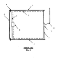
- FIG. 1 is a structural schematic sectional view of a shielding subrack for installing a circuit board 1 in the first prior art.
- Each of the six sides of the subrack is formed of sheet material with shielding layer, typically metal plate.
- the gaps between the upper cover plate 3 and the left, right side plates (not shown in figures) as well as between the lower cover plate 4 and the left, right side plates are fixed by screws or rivets 9 with each other.
- the distance between the screws or rivets 9 is required to meet the shielding requirements and is typically 20-60 mm.
- Shielding materials are arranged in the active gaps between the front panel 5, the rear cover plate 6 and the other plates. In such a way, the six metal sides of the subrack form a shielding chamber, and the external-interfacing signal line 10 of the circuit board is generally led out from the connector 7 arranged on the front panel.
- each of the six sides of the subrack is a metal plate and the shielding materials are arranged in the active gaps of the front panel and the rear cover plate, the shielding cost is high.
- the rear shielding cover plate occupies a certain space, in the case that the depth dimension of the subrack is limited, the effective depth dimension provided for the circuit board within the subrack will be reduced, which configuration is adverse to the installation of boards carrying traffic with high density.
- FIG. 2 is a structural schematic sectional view of a shielding subrack for installing a circuit board 1 in the second prior art.
- Each of the six sides of the subrack is formed of sheet material with shielding layer, typically a metal plate.
- the gaps between the upper cover plate 3 and the left, right side plates (not shown in figures) as well as between the lower cover plate 4 and the left, right side plates are fixed by screws or rivets 9 with each other.
- the distance between the screws or rivets 9 is required to meet the shielding requirements and is typically 20-60 mm.
- Shielding materials are arranged in the active gaps between the front panel 5, the rear cover plate 6 and the other plates.
- the backplane 2 is firstly installed in the back of the subrack.
- the backplane 2 is a printed circuit board and extends upward beyond the subrack.
- the rear shielding cover plate 6 then is installed behind the backplane 2.
- the rear shielding cover plate 6 is connected with the subrack at the periphery thereof by screws 9 to keep electromagnetic sealing.
- the external-interfacing signal line 10 runs inside the backplane and goes to the output-line area above the backplane, then is led out via the connector 7 in the output-line area.
- each of the six sides of the subrack is a metal plate and shielding material are arranged in the active gaps of the front panel and the rear cover plate, the shielding cost is high.
- a great number of signal lines need to be connected via the backplane, as a result, the number of the backplane's layers increases, and thus the cost of the backplane, are largely increased.
- the signal lines being connected via the backplane results in an increased height of the whole subrack, which in turn causes the number of subracks installed in the equipment cabinet to be reduced, thereby decreasing the total working capacity and also increasing the costs indirectly.
- JP-A-09 006468 (TOSHIBA KK) to take, which discloses a circuit substrate rack having ground layer provided at backplane.
- the present invention discloses a shielding subrack module to solve the problems of high cost and large volume existed in the shielding subrack of the prior arts.
- a subrack body having an upper cover plate, a lower cover plate, a front panel, a left side plate and a right side plate; and a backplane whose edges fixedly connected to the peripheral hem of the subrack body, the backplane being a printed circuit board, wherein both surfaces of the backplane are covered by shielding copper sheet with no traces, and each of the upper cover plate, the lower cover plate, the front panel, the left side plate and the right side plate includes a shielding layer.
- the backplane has an insulating layer coated on the surfaces of the shielding copper sheets.
- the insulating layer is coated on the surfaces other than joining surface of the shielding copper sheet of the backplane with the peripheral hem of the subrack body.
- the upper cover plate, the lower cover plate, the front panel, the left side plate and the right side plate are respectively fixedly connected by screws or rivets.
- the backplane and the peripheral hem of the subrack body are fixedly connected each other by screws or rivets.
- the distance between the screws or the rivets ranges from 20 to 60 mm.
- Shielding materials are arranged in the gaps between the front panel and the upper cover plate, the lower cover plate, the left side plate and the right side plate.
- the subrack module further comprises a circuit board installed in the subrack body, and the circuit board is electrically connected to the backplane by a first connector arranged on the backplane.
- the circuit board is further electrically connected to an external-interfacing signal line by the first connector.
- the subrack module further comprises a second connector arranged on the front panel; and the circuit board is electrically connected to the external-interfacing signal line by the second connector.
- the object of the invention is to provide a simplified subrack shielding design which lowers the shielding cost and reduces the volume of the subrack.
- the technical concept of the present invention lies in that a backplane which is a printed circuit board whose surface/surfaces is/are covered by non-wiring copper sheets is utilized to directly function as a shield body and the rear cover plate is omitted, which in one respect lowers the shielding cost, and in the other respect, reduces the volume of the subrack and saves valuable space in the electronic products.
- FIG 3 is a structural schematic sectional view of the shielding subrack in accordance with the present invention.
- the shielding subrack includes a backplane 2 of the circuit board 1, an upper cover plate 3, a lower cover plate 4, left and right side plates (not shown in Figure 3 ), and a front panel 5.
- the backplane 2 is a printed circuit board, while the other plates are made of sheet material with a shielding layer, typically a metal plate.
- the gaps between the upper and lower cover plates as well as the left, right side plates are fixed by screws or rivet with each other. Shielding materials are arranged in the active gaps between the front panel 5 and the upper cover plate 3, the lower cover plate 4, the left, right side plates (not shown in Figure 3 ).
- the backplane 2 acts directly as a shielding body.
- the EMC design requirements of the backplane 2 are as follows: the backplane is a printed circuit board, and both of surface layer and bottom layer are completely covered by copper and have no traces, so as to form a shielding copper sheet; among the surfaces of the shielding copper sheet, except that the joining surface of the peripheral surface layer of the backplane with the subrack is bare copper, the remaining surface can be coated with an insulating layer.
- the bare copper is provided to achieve an effective electrical connection between the backplane 2 and the peripheral hem of the subrack, to minimize the gap therebetween, and to improve the effect of the electromagnetic shielding.
- Screw holes are arranged in the upper, lower, left and right peripheral edges of the backplane 2, and the distance between the screw holes ranges from 20 to 60 mm.
- the peripheral edges of the backplane 2 are connected with the peripheral hem of the subrack by screws to attain joint electromagnetic sealing between the backplane 2 and the subrack.
- the distance between screws or rivets 9 meets the shielding requirement and is typically 20-60 mm.
- an.external-interfacing signal line of the subrack is led out from the backside of the backplane 2.
- the circuit board 1 is electrically connected with the external-interfacing signal line 10 through a connector 8 between the circuit board 1 and the backplane 2.
- the second embodiment is similar to the first one.
- the shielding subrack includes a backplane 2 of the circuit board 1, an upper cover plate 3, a lower cover plate 4, left and right side plates (not shown in Figure 4 ), and a front panel 5, wherein the backplane 2 is a printed circuit board, while the other plates are made of sheet material with a shielding layer, typically a metal plate.
- the gaps between the upper, lower cover plates as well as the left and right side plates are fixed by screws or rivets with each other. Shielding materials are arranged in the active gaps between the front panel 5 and the upper cover plate 3, the lower cover plate 4, the left and right side plates (not shown in Figure 4 ).
- the backplane 2 acts directly as a shielding body.
- the EMC design requirements of the backplane 2 are as follows: the backplane is a printed circuit board, and both of surface layer and bottom layer are completely covered by copper and have no traces so as to form a shielding copper sheet; among the surfaces of the shielding copper sheet, except that the joining surface of the peripheral surface layer of the backplane with the subrack is bare copper, the remaining surface can be coated with an insulating layer.
- the bare copper is provided to achieve an effective electrical connection between the backplane 2 and the peripheral hem of the subrack, to minimize the gap therebetween, and to improve the effect of the electromagnetic shielding.
- Screw holes are arranged in the upper, lower, left and right peripheral edges of the backplane 2, and the distance between the screw holes ranges from 20 to 60 mm.
- the peripheral edges of the backplane 2 are connected with the peripheral hem of the subrack by screws to attain joint electromagnetic sealing between the backplane and the subrack.
- the distance between screws or rivets 9 meets the shielding requirement and is typically 20-60 mm.
- the external-interfacing signal line 10 is led out from the front of the subrack.
- the circuit board 1 is electrically connected with the external-interfacing signal line 10 through a connector 7 arranged on the front panel 5.
Landscapes
- Engineering & Computer Science (AREA)
- Microelectronics & Electronic Packaging (AREA)
- Shielding Devices Or Components To Electric Or Magnetic Fields (AREA)
- Fire-Detection Mechanisms (AREA)
- Mounting Of Printed Circuit Boards And The Like (AREA)
Claims (10)
- Abschirmendes Baugruppenträger-Modul, umfassend:einen Grundkörper des Baugruppenträgers, welcher umfasst eine obere Deckplatte (3), eine untere Deckplatte (4), ein Frontpaneel (5), eine linke Platte und eine rechte Platte, und eine Rückwandplatine (2), deren Kanten fest mit der Randumfassung des Grundkörpers des Baugruppenträgers verbunden sind und wobei die Rückwandplatine (2) eine Leiterplatte ist,dadurch gekennzeichnet, dass beide Oberflächen der Rückwandplatine (2) durch abschirmendes Kupferblech ohne Leiterbahnen bedeckt sind und die obere Deckplatte (3), die untere Deckplatte (4), das Frontpaneel (5), die linke Platte und die rechte Platte jeweils eine Abschirmungsschicht umfassen.
- Abschirmendes Baugruppenträger-Modul nach Anspruch 1, dadurch gekennzeichnet, dass eine Isolierschicht auf der Oberfläche des abschirmenden Kupferblechs aufgebracht ist.
- Abschirmendes Baugruppenträger-Modul nach Anspruch 2, dadurch gekennzeichnet, dass die Isolierschicht auf der anderen Oberfläche als der Verbindungsoberfläche des abschirmenden Kupferblechs der Rückwandplatine (2) zu der Randumfassung des Grundkörpers des Baugruppenträgers aufgebracht ist.
- Abschirmendes Baugruppenträger-Modul nach Anspruch 1, 2 oder 3, dadurch gekennzeichnet, dass die obere Deckplatte (3), die untere Deckplatte (4), das Frontpaneel (5), die linke Platte und die rechte Platte jeweils durch Schrauben oder Nieten (9) fest verbunden sind.
- Abschirmendes Baugruppenträger-Modul nach Anspruch 4, dadurch gekennzeichnet, dass die Rückwandplatine (2) und die Randumfassung des Grundkörpers des Baugruppenträgers durch Schrauben oder Nieten (9) fest miteinander verbunden sind.
- Abschirmendes Baugruppenträger-Modul nach Anspruch 5, dadurch gekennzeichnet, dass sich die Entfernung zwischen den Schrauben bzw. den Nieten (9) in einem Bereich von 20 bis 60 mm befindet.
- Abschirmendes Baugruppenträger-Modul nach Anspruch 1, dadurch gekennzeichnet, dass Abschirmungsmaterialien in Spalten zwischen dem Frontpaneel (5) und der oberen Deckplatte (3), der unteren Deckplatte (4), der linken Seitenplatte und der rechten Seitenplatte angeordnet sind.
- Abschirmendes Baugruppenträger-Modul nach Anspruch 1, 2 oder 3, dadurch gekennzeichnet, dass das Baugruppenträger-Modul ferner eine Leiterplatte (1) umfasst, welche in dem Grundkörper des Baugruppenträgers installiert ist, und die Leiterplatte (1) durch einen ersten Verbinder (8), welcher an der Rückwandplatine (2) angeordnet ist, elektrisch mit der Rückwandplatine (2) verbunden ist.
- Abschirmendes Baugruppenträger-Modul nach Anspruch 8, dadurch gekennzeichnet, dass die Leiterplatte (1) durch den ersten Verbinder (8) ferner elektrisch mit einer Signalleitung (10) zur externen Verbindung verbunden ist.
- Abschirmendes Baugruppenträger-Modul nach Anspruch 8, dadurch gekennzeichnet, dass das Baugruppenträger-Modul ferner einen zweiten Verbinder (7) umfasst, welcher an dem Frontpaneel (5) angeordnet ist, und die Leiterplatte (1) durch den zweiten Verbinder (7) elektrisch mit der Signalleitung (10) zur externen Verbindung verbunden ist.
Applications Claiming Priority (2)
| Application Number | Priority Date | Filing Date | Title |
|---|---|---|---|
| CNU200520106557XU CN2862613Y (zh) | 2005-08-31 | 2005-08-31 | 一种屏蔽插框组件 |
| PCT/CN2006/001353 WO2007025430A1 (fr) | 2005-08-31 | 2006-06-16 | Module panneau de connexion à broches pour blindage |
Publications (3)
| Publication Number | Publication Date |
|---|---|
| EP1921905A1 EP1921905A1 (de) | 2008-05-14 |
| EP1921905A4 EP1921905A4 (de) | 2008-10-15 |
| EP1921905B1 true EP1921905B1 (de) | 2009-08-05 |
Family
ID=37660241
Family Applications (1)
| Application Number | Title | Priority Date | Filing Date |
|---|---|---|---|
| EP06742180A Not-in-force EP1921905B1 (de) | 2005-08-31 | 2006-06-16 | Abschirmendes pinboard-modul |
Country Status (6)
| Country | Link |
|---|---|
| EP (1) | EP1921905B1 (de) |
| CN (1) | CN2862613Y (de) |
| AT (1) | ATE439029T1 (de) |
| DE (1) | DE602006008321D1 (de) |
| ES (1) | ES2329077T3 (de) |
| WO (1) | WO2007025430A1 (de) |
Families Citing this family (2)
| Publication number | Priority date | Publication date | Assignee | Title |
|---|---|---|---|---|
| CN102724858B (zh) * | 2012-06-13 | 2016-01-27 | 华为技术有限公司 | 一种插框及其屏蔽背板 |
| CN107041115B (zh) * | 2017-05-22 | 2019-06-04 | 中国电子科技集团公司第四十一研究所 | 一种kvm一体机电磁兼容屏蔽腔 |
Family Cites Families (4)
| Publication number | Priority date | Publication date | Assignee | Title |
|---|---|---|---|---|
| JPH096468A (ja) * | 1995-06-16 | 1997-01-10 | Toshiba Corp | 電子機器 |
| CN1189085A (zh) * | 1996-12-11 | 1998-07-29 | 阿尔卑斯电气株式会社 | 电子机器 |
| CN2523118Y (zh) * | 2002-02-09 | 2002-11-27 | 深圳市中兴通讯股份有限公司上海第二研究所 | 用于通讯设备插箱中的导轨装置 |
| CN2718736Y (zh) * | 2004-03-31 | 2005-08-17 | 华为技术有限公司 | 一种屏蔽装置 |
-
2005
- 2005-08-31 CN CNU200520106557XU patent/CN2862613Y/zh not_active Expired - Lifetime
-
2006
- 2006-06-16 EP EP06742180A patent/EP1921905B1/de not_active Not-in-force
- 2006-06-16 DE DE602006008321T patent/DE602006008321D1/de active Active
- 2006-06-16 AT AT06742180T patent/ATE439029T1/de not_active IP Right Cessation
- 2006-06-16 ES ES06742180T patent/ES2329077T3/es active Active
- 2006-06-16 WO PCT/CN2006/001353 patent/WO2007025430A1/zh not_active Ceased
Also Published As
| Publication number | Publication date |
|---|---|
| CN2862613Y (zh) | 2007-01-24 |
| EP1921905A4 (de) | 2008-10-15 |
| ATE439029T1 (de) | 2009-08-15 |
| WO2007025430A1 (fr) | 2007-03-08 |
| EP1921905A1 (de) | 2008-05-14 |
| DE602006008321D1 (de) | 2009-09-17 |
| ES2329077T3 (es) | 2009-11-20 |
Similar Documents
| Publication | Publication Date | Title |
|---|---|---|
| US5596487A (en) | Apparatus for RF shielding radio circuitry | |
| EP1418798B1 (de) | Leiterplatte und Methode um eine Leiterplatte an einem elektrisch leitenden Gehäuse anzubringen | |
| WO2004091055B1 (en) | Shielding cage with improved emi shielding gasket construction | |
| US6490438B1 (en) | Mobile phone having an improved shielded device | |
| US20080047746A1 (en) | Shield assembly with gaskets | |
| WO2004088381B1 (en) | Shielding cage with multiple module-receiving bays | |
| CN113835269B (zh) | 一种背光模组及显示装置 | |
| TWI440930B (zh) | 平面顯示模組 | |
| DE102006049567B4 (de) | Abschirmungsaufbau für Einrichtungen der Informationstechnik | |
| EP2063698A1 (de) | Plasmaanzeigevorrichtung | |
| US7492609B2 (en) | Flat panel display with single shielded circuit board | |
| US6963495B1 (en) | EMI shielded chassis for electrical circuitry | |
| US6116924A (en) | Electromagnetic emissions shielding structure for circuit board connector assembly | |
| EP2607947A2 (de) | Anzeigevorrichtung mit elektromagnetischer Wellenabschirmstruktur | |
| EP1921905A1 (de) | Abschirmendes pinboard-modul | |
| CN101498960A (zh) | 一种制造具有良好电磁兼容性能的计算机的方法 | |
| CN106659102A (zh) | 一种强电磁脉冲屏蔽防护加固机箱 | |
| US6508653B2 (en) | Computer system bulkhead plate for attenuating electromagnetic interference (EMI) at a telephone jack connector | |
| US20130277102A1 (en) | Electromagnetic Interference Blocking Cabinet with Integrated Input/Output Panel | |
| CN212324652U (zh) | 一种电磁屏蔽腔体结构 | |
| CN2657345Y (zh) | 屏蔽收纳壳体组合 | |
| CN101592806B (zh) | 面板显示装置 | |
| CN224205502U (zh) | 一种电磁屏蔽插卡机箱 | |
| CN2603536Y (zh) | 内置板卡接口元件的接地装置 | |
| CN201001254Y (zh) | 电路组件箱隔板 |
Legal Events
| Date | Code | Title | Description |
|---|---|---|---|
| PUAI | Public reference made under article 153(3) epc to a published international application that has entered the european phase |
Free format text: ORIGINAL CODE: 0009012 |
|
| 17P | Request for examination filed |
Effective date: 20080225 |
|
| AK | Designated contracting states |
Kind code of ref document: A1 Designated state(s): AT BE BG CH CY CZ DE DK EE ES FI FR GB GR HU IE IS IT LI LT LU LV MC NL PL PT RO SE SI SK TR |
|
| A4 | Supplementary search report drawn up and despatched |
Effective date: 20080811 |
|
| RIC1 | Information provided on ipc code assigned before grant |
Ipc: H05K 9/00 20060101ALI20080805BHEP Ipc: H04Q 1/10 20060101ALI20080805BHEP Ipc: H05K 7/14 20060101AFI20080805BHEP |
|
| RA4 | Supplementary search report drawn up and despatched (corrected) |
Effective date: 20080911 |
|
| GRAP | Despatch of communication of intention to grant a patent |
Free format text: ORIGINAL CODE: EPIDOSNIGR1 |
|
| GRAS | Grant fee paid |
Free format text: ORIGINAL CODE: EPIDOSNIGR3 |
|
| GRAA | (expected) grant |
Free format text: ORIGINAL CODE: 0009210 |
|
| AK | Designated contracting states |
Kind code of ref document: B1 Designated state(s): AT BE BG CH CY CZ DE DK EE ES FI FR GB GR HU IE IS IT LI LT LU LV MC NL PL PT RO SE SI SK TR |
|
| REG | Reference to a national code |
Ref country code: GB Ref legal event code: FG4D |
|
| REG | Reference to a national code |
Ref country code: CH Ref legal event code: EP |
|
| REG | Reference to a national code |
Ref country code: IE Ref legal event code: FG4D |
|
| REF | Corresponds to: |
Ref document number: 602006008321 Country of ref document: DE Date of ref document: 20090917 Kind code of ref document: P |
|
| REG | Reference to a national code |
Ref country code: DE Ref legal event code: R096 Ref document number: 602006008321 Country of ref document: DE Effective date: 20090917 |
|
| REG | Reference to a national code |
Ref country code: SE Ref legal event code: TRGR |
|
| REG | Reference to a national code |
Ref country code: ES Ref legal event code: FG2A Ref document number: 2329077 Country of ref document: ES Kind code of ref document: T3 |
|
| LTIE | Lt: invalidation of european patent or patent extension |
Effective date: 20090805 |
|
| PG25 | Lapsed in a contracting state [announced via postgrant information from national office to epo] |
Ref country code: AT Free format text: LAPSE BECAUSE OF FAILURE TO SUBMIT A TRANSLATION OF THE DESCRIPTION OR TO PAY THE FEE WITHIN THE PRESCRIBED TIME-LIMIT Effective date: 20090805 Ref country code: IS Free format text: LAPSE BECAUSE OF FAILURE TO SUBMIT A TRANSLATION OF THE DESCRIPTION OR TO PAY THE FEE WITHIN THE PRESCRIBED TIME-LIMIT Effective date: 20091205 Ref country code: FI Free format text: LAPSE BECAUSE OF FAILURE TO SUBMIT A TRANSLATION OF THE DESCRIPTION OR TO PAY THE FEE WITHIN THE PRESCRIBED TIME-LIMIT Effective date: 20090805 Ref country code: LT Free format text: LAPSE BECAUSE OF FAILURE TO SUBMIT A TRANSLATION OF THE DESCRIPTION OR TO PAY THE FEE WITHIN THE PRESCRIBED TIME-LIMIT Effective date: 20090805 |
|
| NLV1 | Nl: lapsed or annulled due to failure to fulfill the requirements of art. 29p and 29m of the patents act | ||
| PG25 | Lapsed in a contracting state [announced via postgrant information from national office to epo] |
Ref country code: SI Free format text: LAPSE BECAUSE OF FAILURE TO SUBMIT A TRANSLATION OF THE DESCRIPTION OR TO PAY THE FEE WITHIN THE PRESCRIBED TIME-LIMIT Effective date: 20090805 Ref country code: NL Free format text: LAPSE BECAUSE OF FAILURE TO SUBMIT A TRANSLATION OF THE DESCRIPTION OR TO PAY THE FEE WITHIN THE PRESCRIBED TIME-LIMIT Effective date: 20090805 Ref country code: PL Free format text: LAPSE BECAUSE OF FAILURE TO SUBMIT A TRANSLATION OF THE DESCRIPTION OR TO PAY THE FEE WITHIN THE PRESCRIBED TIME-LIMIT Effective date: 20090805 Ref country code: LV Free format text: LAPSE BECAUSE OF FAILURE TO SUBMIT A TRANSLATION OF THE DESCRIPTION OR TO PAY THE FEE WITHIN THE PRESCRIBED TIME-LIMIT Effective date: 20090805 |
|
| PG25 | Lapsed in a contracting state [announced via postgrant information from national office to epo] |
Ref country code: BG Free format text: LAPSE BECAUSE OF FAILURE TO SUBMIT A TRANSLATION OF THE DESCRIPTION OR TO PAY THE FEE WITHIN THE PRESCRIBED TIME-LIMIT Effective date: 20091105 Ref country code: PT Free format text: LAPSE BECAUSE OF FAILURE TO SUBMIT A TRANSLATION OF THE DESCRIPTION OR TO PAY THE FEE WITHIN THE PRESCRIBED TIME-LIMIT Effective date: 20091205 |
|
| PG25 | Lapsed in a contracting state [announced via postgrant information from national office to epo] |
Ref country code: CZ Free format text: LAPSE BECAUSE OF FAILURE TO SUBMIT A TRANSLATION OF THE DESCRIPTION OR TO PAY THE FEE WITHIN THE PRESCRIBED TIME-LIMIT Effective date: 20090805 Ref country code: DK Free format text: LAPSE BECAUSE OF FAILURE TO SUBMIT A TRANSLATION OF THE DESCRIPTION OR TO PAY THE FEE WITHIN THE PRESCRIBED TIME-LIMIT Effective date: 20090805 Ref country code: RO Free format text: LAPSE BECAUSE OF FAILURE TO SUBMIT A TRANSLATION OF THE DESCRIPTION OR TO PAY THE FEE WITHIN THE PRESCRIBED TIME-LIMIT Effective date: 20090805 Ref country code: EE Free format text: LAPSE BECAUSE OF FAILURE TO SUBMIT A TRANSLATION OF THE DESCRIPTION OR TO PAY THE FEE WITHIN THE PRESCRIBED TIME-LIMIT Effective date: 20090805 |
|
| PG25 | Lapsed in a contracting state [announced via postgrant information from national office to epo] |
Ref country code: SK Free format text: LAPSE BECAUSE OF FAILURE TO SUBMIT A TRANSLATION OF THE DESCRIPTION OR TO PAY THE FEE WITHIN THE PRESCRIBED TIME-LIMIT Effective date: 20090805 |
|
| PLBE | No opposition filed within time limit |
Free format text: ORIGINAL CODE: 0009261 |
|
| STAA | Information on the status of an ep patent application or granted ep patent |
Free format text: STATUS: NO OPPOSITION FILED WITHIN TIME LIMIT |
|
| PG25 | Lapsed in a contracting state [announced via postgrant information from national office to epo] |
Ref country code: BE Free format text: LAPSE BECAUSE OF FAILURE TO SUBMIT A TRANSLATION OF THE DESCRIPTION OR TO PAY THE FEE WITHIN THE PRESCRIBED TIME-LIMIT Effective date: 20090805 |
|
| 26N | No opposition filed |
Effective date: 20100507 |
|
| REG | Reference to a national code |
Ref country code: DE Ref legal event code: R097 Ref document number: 602006008321 Country of ref document: DE Effective date: 20100507 |
|
| PG25 | Lapsed in a contracting state [announced via postgrant information from national office to epo] |
Ref country code: GR Free format text: LAPSE BECAUSE OF FAILURE TO SUBMIT A TRANSLATION OF THE DESCRIPTION OR TO PAY THE FEE WITHIN THE PRESCRIBED TIME-LIMIT Effective date: 20091106 |
|
| PG25 | Lapsed in a contracting state [announced via postgrant information from national office to epo] |
Ref country code: MC Free format text: LAPSE BECAUSE OF NON-PAYMENT OF DUE FEES Effective date: 20100630 |
|
| REG | Reference to a national code |
Ref country code: CH Ref legal event code: PL |
|
| PG25 | Lapsed in a contracting state [announced via postgrant information from national office to epo] |
Ref country code: IT Free format text: LAPSE BECAUSE OF FAILURE TO SUBMIT A TRANSLATION OF THE DESCRIPTION OR TO PAY THE FEE WITHIN THE PRESCRIBED TIME-LIMIT Effective date: 20090805 |
|
| PG25 | Lapsed in a contracting state [announced via postgrant information from national office to epo] |
Ref country code: IE Free format text: LAPSE BECAUSE OF NON-PAYMENT OF DUE FEES Effective date: 20100616 Ref country code: LI Free format text: LAPSE BECAUSE OF NON-PAYMENT OF DUE FEES Effective date: 20100630 Ref country code: CH Free format text: LAPSE BECAUSE OF NON-PAYMENT OF DUE FEES Effective date: 20100630 |
|
| PG25 | Lapsed in a contracting state [announced via postgrant information from national office to epo] |
Ref country code: CY Free format text: LAPSE BECAUSE OF FAILURE TO SUBMIT A TRANSLATION OF THE DESCRIPTION OR TO PAY THE FEE WITHIN THE PRESCRIBED TIME-LIMIT Effective date: 20090805 |
|
| PG25 | Lapsed in a contracting state [announced via postgrant information from national office to epo] |
Ref country code: LU Free format text: LAPSE BECAUSE OF NON-PAYMENT OF DUE FEES Effective date: 20100616 Ref country code: HU Free format text: LAPSE BECAUSE OF FAILURE TO SUBMIT A TRANSLATION OF THE DESCRIPTION OR TO PAY THE FEE WITHIN THE PRESCRIBED TIME-LIMIT Effective date: 20100206 |
|
| PG25 | Lapsed in a contracting state [announced via postgrant information from national office to epo] |
Ref country code: TR Free format text: LAPSE BECAUSE OF FAILURE TO SUBMIT A TRANSLATION OF THE DESCRIPTION OR TO PAY THE FEE WITHIN THE PRESCRIBED TIME-LIMIT Effective date: 20090805 |
|
| REG | Reference to a national code |
Ref country code: FR Ref legal event code: PLFP Year of fee payment: 11 |
|
| REG | Reference to a national code |
Ref country code: FR Ref legal event code: PLFP Year of fee payment: 12 |
|
| REG | Reference to a national code |
Ref country code: FR Ref legal event code: PLFP Year of fee payment: 13 |
|
| P01 | Opt-out of the competence of the unified patent court (upc) registered |
Effective date: 20230524 |
|
| PGFP | Annual fee paid to national office [announced via postgrant information from national office to epo] |
Ref country code: ES Payment date: 20230711 Year of fee payment: 18 |
|
| PGFP | Annual fee paid to national office [announced via postgrant information from national office to epo] |
Ref country code: GB Payment date: 20240502 Year of fee payment: 19 |
|
| PGFP | Annual fee paid to national office [announced via postgrant information from national office to epo] |
Ref country code: DE Payment date: 20240502 Year of fee payment: 19 |
|
| PGFP | Annual fee paid to national office [announced via postgrant information from national office to epo] |
Ref country code: FR Payment date: 20240509 Year of fee payment: 19 |
|
| PGFP | Annual fee paid to national office [announced via postgrant information from national office to epo] |
Ref country code: SE Payment date: 20240510 Year of fee payment: 19 |
|
| REG | Reference to a national code |
Ref country code: ES Ref legal event code: FD2A Effective date: 20250731 |
|
| PG25 | Lapsed in a contracting state [announced via postgrant information from national office to epo] |
Ref country code: ES Free format text: LAPSE BECAUSE OF NON-PAYMENT OF DUE FEES Effective date: 20240617 |
|
| REG | Reference to a national code |
Ref country code: DE Ref legal event code: R119 Ref document number: 602006008321 Country of ref document: DE |
|
| REG | Reference to a national code |
Ref country code: SE Ref legal event code: EUG |
|
| GBPC | Gb: european patent ceased through non-payment of renewal fee |
Effective date: 20250616 |
|
| PG25 | Lapsed in a contracting state [announced via postgrant information from national office to epo] |
Ref country code: GB Free format text: LAPSE BECAUSE OF NON-PAYMENT OF DUE FEES Effective date: 20250616 |
|
| PG25 | Lapsed in a contracting state [announced via postgrant information from national office to epo] |
Ref country code: DE Free format text: LAPSE BECAUSE OF NON-PAYMENT OF DUE FEES Effective date: 20260101 |
|
| PG25 | Lapsed in a contracting state [announced via postgrant information from national office to epo] |
Ref country code: FR Free format text: LAPSE BECAUSE OF NON-PAYMENT OF DUE FEES Effective date: 20250630 |