EP2600411A1 - Method for manufacturing light-absorbing substrate and method for manufacturing die for manufacturing light-absorbing substrate - Google Patents
Method for manufacturing light-absorbing substrate and method for manufacturing die for manufacturing light-absorbing substrate Download PDFInfo
- Publication number
- EP2600411A1 EP2600411A1 EP11812315.7A EP11812315A EP2600411A1 EP 2600411 A1 EP2600411 A1 EP 2600411A1 EP 11812315 A EP11812315 A EP 11812315A EP 2600411 A1 EP2600411 A1 EP 2600411A1
- Authority
- EP
- European Patent Office
- Prior art keywords
- substrate
- light
- manufacturing
- depressions
- laser light
- Prior art date
- Legal status (The legal status is an assumption and is not a legal conclusion. Google has not performed a legal analysis and makes no representation as to the accuracy of the status listed.)
- Granted
Links
- 239000000758 substrate Substances 0.000 title claims abstract description 162
- 238000004519 manufacturing process Methods 0.000 title claims abstract description 55
- 238000000034 method Methods 0.000 title claims abstract description 49
- 238000005530 etching Methods 0.000 claims abstract description 38
- 230000001678 irradiating effect Effects 0.000 claims abstract description 5
- 230000010287 polarization Effects 0.000 claims description 8
- KWYUFKZDYYNOTN-UHFFFAOYSA-M Potassium hydroxide Chemical compound [OH-].[K+] KWYUFKZDYYNOTN-UHFFFAOYSA-M 0.000 description 15
- 239000000463 material Substances 0.000 description 14
- 230000015572 biosynthetic process Effects 0.000 description 12
- NBIIXXVUZAFLBC-UHFFFAOYSA-N Phosphoric acid Chemical compound OP(O)(O)=O NBIIXXVUZAFLBC-UHFFFAOYSA-N 0.000 description 9
- 229910052751 metal Inorganic materials 0.000 description 7
- 239000002184 metal Substances 0.000 description 7
- MHAJPDPJQMAIIY-UHFFFAOYSA-N Hydrogen peroxide Chemical compound OO MHAJPDPJQMAIIY-UHFFFAOYSA-N 0.000 description 6
- PXHVJJICTQNCMI-UHFFFAOYSA-N Nickel Chemical compound [Ni] PXHVJJICTQNCMI-UHFFFAOYSA-N 0.000 description 6
- QAOWNCQODCNURD-UHFFFAOYSA-N Sulfuric acid Chemical compound OS(O)(=O)=O QAOWNCQODCNURD-UHFFFAOYSA-N 0.000 description 6
- QTBSBXVTEAMEQO-UHFFFAOYSA-N Acetic acid Chemical compound CC(O)=O QTBSBXVTEAMEQO-UHFFFAOYSA-N 0.000 description 5
- XUIMIQQOPSSXEZ-UHFFFAOYSA-N Silicon Chemical compound [Si] XUIMIQQOPSSXEZ-UHFFFAOYSA-N 0.000 description 5
- 239000007788 liquid Substances 0.000 description 5
- 239000011159 matrix material Substances 0.000 description 5
- 229910052710 silicon Inorganic materials 0.000 description 5
- 239000010703 silicon Substances 0.000 description 5
- XLYOFNOQVPJJNP-UHFFFAOYSA-N water Substances O XLYOFNOQVPJJNP-UHFFFAOYSA-N 0.000 description 5
- KRHYYFGTRYWZRS-UHFFFAOYSA-N Fluorane Chemical compound F KRHYYFGTRYWZRS-UHFFFAOYSA-N 0.000 description 4
- GRYLNZFGIOXLOG-UHFFFAOYSA-N Nitric acid Chemical compound O[N+]([O-])=O GRYLNZFGIOXLOG-UHFFFAOYSA-N 0.000 description 4
- 230000000295 complement effect Effects 0.000 description 4
- 229910017604 nitric acid Inorganic materials 0.000 description 4
- WGTYBPLFGIVFAS-UHFFFAOYSA-M tetramethylammonium hydroxide Chemical compound [OH-].C[N+](C)(C)C WGTYBPLFGIVFAS-UHFFFAOYSA-M 0.000 description 4
- VHUUQVKOLVNVRT-UHFFFAOYSA-N Ammonium hydroxide Chemical compound [NH4+].[OH-] VHUUQVKOLVNVRT-UHFFFAOYSA-N 0.000 description 3
- VEXZGXHMUGYJMC-UHFFFAOYSA-N Hydrochloric acid Chemical compound Cl VEXZGXHMUGYJMC-UHFFFAOYSA-N 0.000 description 3
- VYPSYNLAJGMNEJ-UHFFFAOYSA-N Silicium dioxide Chemical compound O=[Si]=O VYPSYNLAJGMNEJ-UHFFFAOYSA-N 0.000 description 3
- HEMHJVSKTPXQMS-UHFFFAOYSA-M Sodium hydroxide Chemical compound [OH-].[Na+] HEMHJVSKTPXQMS-UHFFFAOYSA-M 0.000 description 3
- 229910000147 aluminium phosphate Inorganic materials 0.000 description 3
- 230000000873 masking effect Effects 0.000 description 3
- 229910052759 nickel Inorganic materials 0.000 description 3
- OAKJQQAXSVQMHS-UHFFFAOYSA-N Hydrazine Chemical compound NN OAKJQQAXSVQMHS-UHFFFAOYSA-N 0.000 description 2
- 238000010521 absorption reaction Methods 0.000 description 2
- LDDQLRUQCUTJBB-UHFFFAOYSA-N ammonium fluoride Chemical compound [NH4+].[F-] LDDQLRUQCUTJBB-UHFFFAOYSA-N 0.000 description 2
- HUCVOHYBFXVBRW-UHFFFAOYSA-M caesium hydroxide Chemical compound [OH-].[Cs+] HUCVOHYBFXVBRW-UHFFFAOYSA-M 0.000 description 2
- 230000007547 defect Effects 0.000 description 2
- 230000002401 inhibitory effect Effects 0.000 description 2
- 239000000243 solution Substances 0.000 description 2
- MIMUSZHMZBJBPO-UHFFFAOYSA-N 6-methoxy-8-nitroquinoline Chemical compound N1=CC=CC2=CC(OC)=CC([N+]([O-])=O)=C21 MIMUSZHMZBJBPO-UHFFFAOYSA-N 0.000 description 1
- 229910001218 Gallium arsenide Inorganic materials 0.000 description 1
- OKKJLVBELUTLKV-UHFFFAOYSA-N Methanol Chemical compound OC OKKJLVBELUTLKV-UHFFFAOYSA-N 0.000 description 1
- HEMINMLPKZELPP-UHFFFAOYSA-N Phosdiphen Chemical compound C=1C=C(Cl)C=C(Cl)C=1OP(=O)(OCC)OC1=CC=C(Cl)C=C1Cl HEMINMLPKZELPP-UHFFFAOYSA-N 0.000 description 1
- 239000000908 ammonium hydroxide Substances 0.000 description 1
- 239000007864 aqueous solution Substances 0.000 description 1
- GZUXJHMPEANEGY-UHFFFAOYSA-N bromomethane Chemical compound BrC GZUXJHMPEANEGY-UHFFFAOYSA-N 0.000 description 1
- 230000015556 catabolic process Effects 0.000 description 1
- 238000006243 chemical reaction Methods 0.000 description 1
- 238000007598 dipping method Methods 0.000 description 1
- 230000000694 effects Effects 0.000 description 1
- 239000011521 glass Substances 0.000 description 1
- 239000000155 melt Substances 0.000 description 1
- 239000010453 quartz Substances 0.000 description 1
- 229910052594 sapphire Inorganic materials 0.000 description 1
- 239000010980 sapphire Substances 0.000 description 1
- 229920006395 saturated elastomer Polymers 0.000 description 1
- 239000000377 silicon dioxide Substances 0.000 description 1
Images






Classifications
-
- H—ELECTRICITY
- H10—SEMICONDUCTOR DEVICES; ELECTRIC SOLID-STATE DEVICES NOT OTHERWISE PROVIDED FOR
- H10F—INORGANIC SEMICONDUCTOR DEVICES SENSITIVE TO INFRARED RADIATION, LIGHT, ELECTROMAGNETIC RADIATION OF SHORTER WAVELENGTH OR CORPUSCULAR RADIATION
- H10F10/00—Individual photovoltaic cells, e.g. solar cells
-
- B—PERFORMING OPERATIONS; TRANSPORTING
- B23—MACHINE TOOLS; METAL-WORKING NOT OTHERWISE PROVIDED FOR
- B23K—SOLDERING OR UNSOLDERING; WELDING; CLADDING OR PLATING BY SOLDERING OR WELDING; CUTTING BY APPLYING HEAT LOCALLY, e.g. FLAME CUTTING; WORKING BY LASER BEAM
- B23K26/00—Working by laser beam, e.g. welding, cutting or boring
- B23K26/352—Working by laser beam, e.g. welding, cutting or boring for surface treatment
- B23K26/355—Texturing
-
- B—PERFORMING OPERATIONS; TRANSPORTING
- B23—MACHINE TOOLS; METAL-WORKING NOT OTHERWISE PROVIDED FOR
- B23K—SOLDERING OR UNSOLDERING; WELDING; CLADDING OR PLATING BY SOLDERING OR WELDING; CUTTING BY APPLYING HEAT LOCALLY, e.g. FLAME CUTTING; WORKING BY LASER BEAM
- B23K26/00—Working by laser beam, e.g. welding, cutting or boring
- B23K26/36—Removing material
- B23K26/361—Removing material for deburring or mechanical trimming
-
- B—PERFORMING OPERATIONS; TRANSPORTING
- B23—MACHINE TOOLS; METAL-WORKING NOT OTHERWISE PROVIDED FOR
- B23K—SOLDERING OR UNSOLDERING; WELDING; CLADDING OR PLATING BY SOLDERING OR WELDING; CUTTING BY APPLYING HEAT LOCALLY, e.g. FLAME CUTTING; WORKING BY LASER BEAM
- B23K26/00—Working by laser beam, e.g. welding, cutting or boring
- B23K26/36—Removing material
- B23K26/362—Laser etching
-
- B—PERFORMING OPERATIONS; TRANSPORTING
- B44—DECORATIVE ARTS
- B44C—PRODUCING DECORATIVE EFFECTS; MOSAICS; TARSIA WORK; PAPERHANGING
- B44C1/00—Processes, not specifically provided for elsewhere, for producing decorative surface effects
- B44C1/22—Removing surface-material, e.g. by engraving, by etching
-
- H—ELECTRICITY
- H10—SEMICONDUCTOR DEVICES; ELECTRIC SOLID-STATE DEVICES NOT OTHERWISE PROVIDED FOR
- H10F—INORGANIC SEMICONDUCTOR DEVICES SENSITIVE TO INFRARED RADIATION, LIGHT, ELECTROMAGNETIC RADIATION OF SHORTER WAVELENGTH OR CORPUSCULAR RADIATION
- H10F71/00—Manufacture or treatment of devices covered by this subclass
-
- H—ELECTRICITY
- H10—SEMICONDUCTOR DEVICES; ELECTRIC SOLID-STATE DEVICES NOT OTHERWISE PROVIDED FOR
- H10F—INORGANIC SEMICONDUCTOR DEVICES SENSITIVE TO INFRARED RADIATION, LIGHT, ELECTROMAGNETIC RADIATION OF SHORTER WAVELENGTH OR CORPUSCULAR RADIATION
- H10F77/00—Constructional details of devices covered by this subclass
- H10F77/70—Surface textures, e.g. pyramid structures
-
- H—ELECTRICITY
- H10—SEMICONDUCTOR DEVICES; ELECTRIC SOLID-STATE DEVICES NOT OTHERWISE PROVIDED FOR
- H10F—INORGANIC SEMICONDUCTOR DEVICES SENSITIVE TO INFRARED RADIATION, LIGHT, ELECTROMAGNETIC RADIATION OF SHORTER WAVELENGTH OR CORPUSCULAR RADIATION
- H10F77/00—Constructional details of devices covered by this subclass
- H10F77/70—Surface textures, e.g. pyramid structures
- H10F77/703—Surface textures, e.g. pyramid structures of the semiconductor bodies, e.g. textured active layers
-
- Y—GENERAL TAGGING OF NEW TECHNOLOGICAL DEVELOPMENTS; GENERAL TAGGING OF CROSS-SECTIONAL TECHNOLOGIES SPANNING OVER SEVERAL SECTIONS OF THE IPC; TECHNICAL SUBJECTS COVERED BY FORMER USPC CROSS-REFERENCE ART COLLECTIONS [XRACs] AND DIGESTS
- Y02—TECHNOLOGIES OR APPLICATIONS FOR MITIGATION OR ADAPTATION AGAINST CLIMATE CHANGE
- Y02E—REDUCTION OF GREENHOUSE GAS [GHG] EMISSIONS, RELATED TO ENERGY GENERATION, TRANSMISSION OR DISTRIBUTION
- Y02E10/00—Energy generation through renewable energy sources
- Y02E10/50—Photovoltaic [PV] energy
Definitions
- this method for manufacturing a mold since at least one of each modified region and a fracture generated from the modified region has reached the surface of the substrate, etching selectively advances from each of the modified regions, so as to form a plurality of depressions on the surface of the substrate.
- positions of the modified regions i.e., positions of the depressions
- Forms of the depressions can be controlled by etching conditions. Since a surface form of the substrate in which positions and forms of the depressions are thus controlled is transferred, a mold formed with depressions and projections complementary to those formed on the surface of the substrate is obtained. Therefore, this method for manufacturing a mold can manufacture a mold which can make a light-absorbing substrate having a surface with depressions and projections formed in a desirable pattern.
Landscapes
- Engineering & Computer Science (AREA)
- Physics & Mathematics (AREA)
- Optics & Photonics (AREA)
- Plasma & Fusion (AREA)
- Mechanical Engineering (AREA)
- Laser Beam Processing (AREA)
- Moulds For Moulding Plastics Or The Like (AREA)
- Weting (AREA)
- Photovoltaic Devices (AREA)
- Diffracting Gratings Or Hologram Optical Elements (AREA)
Abstract
Description
- The present invention relates to a method for manufacturing a light-absorbing substrate employed for a solar battery or the like, for example, and a method for manufacturing a mold for making the same.
- Known as a method for manufacturing a light-absorbing substrate in the above-mentioned technical field is one which, for making depressions and projections on a surface of a substrate, forms a masking pattern on the surface of the substrate and etches the surface of the substrate while using the masking pattern as a mask (see, for example, Patent Literature 1).
- Patent Literature 1: Japanese Patent Application Laid-Open No.
2001-223370 - However, methods for manufacturing a light-absorbing substrate such as the one mentioned above require time and effort to form the masking pattern, though they can control positions and forms of the depressions.
- It is therefore an object of the present invention to provide a method for manufacturing a light-absorbing substrate which can easily manufacture a light-absorbing substrate having a surface with depressions and projections formed in a desirable pattern, and a mold for making the same.
- The method for manufacturing a light-absorbing substrate in accordance with one aspect of the present invention is a method for manufacturing a light-absorbing substrate having a surface with depressions and projections, the method comprising a first step of irradiating a substrate with a laser light so as to form a plurality of modified regions arranged two-dimensionally along a surface of the substrate within the substrate and cause at least one of each modified region and a fracture generated from the modified region to reach the surface of the substrate, and a second step of etching the surface of the substrate after the first step so as to form depressions and projections on the surface of the substrate.
- In this method for manufacturing a light-absorbing substrate, since at least one of each modified region and a fracture generated from the modified region has reached the surface of the substrate, etching selectively advances from each of the modified regions, so as to form a plurality of depressions on the surface of the substrate. Here, positions of the modified regions, i.e., positions of the depressions, can be controlled by irradiation conditions of the laser light. Forms of the depressions can be controlled by etching conditions. Therefore, this method for manufacturing a light-absorbing substrate can easily manufacture a light-absorbing substrate having a surface with depressions and projections formed in a desirable pattern.
- In the second step, anisotropic etching may be performed as the etching. This can inhibit a plurality of depressions produced on the surface of the substrate from fluctuating their forms among them.
- In the second step, isotropic etching may be performed as the etching after the anisotropic etching. This can smoothen the inner faces of a plurality of depressions formed on the surface of the substrate.
- In the first step, the laser light may be relatively moved along the surface of the substrate so as to follow a direction of polarization of the laser light. This can further inhibit the plurality of depressions produced on the surface of the substrate from fluctuating their forms among them.
- In the first step, the substrate may be irradiated with the laser light a plurality of times while changing the distance between the surface of the substrate and a converging point of the laser light so as to form the respective modified regions. This can form the depressions such that the ratio of depth to opening width (aspect ratio) of the depressions becomes greater.
- The method for manufacturing a mold in accordance with one aspect of the present invention is a method for manufacturing a mold for making a light-absorbing substrate having a surface with depressions and projections, the method comprising a first step of irradiating a substrate with a laser light so as to form a plurality of modified regions arranged two-dimensionally along a surface of the substrate within the substrate and cause at least one of each modified region and a fracture generated from the modified region to reach the surface of the substrate, a second step of etching the surface of the substrate after the first step so as to form depressions and projections on the surface of the substrate, and a third step of transferring a form of the surface of the substrate after the second step so as to yield the mold.
- In this method for manufacturing a mold, since at least one of each modified region and a fracture generated from the modified region has reached the surface of the substrate, etching selectively advances from each of the modified regions, so as to form a plurality of depressions on the surface of the substrate. Here, positions of the modified regions, i.e., positions of the depressions, can be controlled by irradiation conditions of the laser light. Forms of the depressions can be controlled by etching conditions. Since a surface form of the substrate in which positions and forms of the depressions are thus controlled is transferred, a mold formed with depressions and projections complementary to those formed on the surface of the substrate is obtained. Therefore, this method for manufacturing a mold can manufacture a mold which can make a light-absorbing substrate having a surface with depressions and projections formed in a desirable pattern.
- The present invention can provide a method for manufacturing a light-absorbing substrate which can easily manufacture a light-absorbing substrate having a surface with depressions, and projections in a desirable pattern and a mold for making the same.
-
- [
Fig. 1 ] is a perspective view of a light-absorbing substrate manufactured by the method for manufacturing a light-absorbing substrate in accordance with an embodiment of the present invention; - [
Fig. 2 ] is a plan view illustrating a first step in the method for manufacturing a light-absorbing substrate in accordance with the embodiment of the present invention; - [
Fig. 3 ] is a sectional view illustrating the first step in the method for manufacturing a light-absorbing substrate in accordance with the embodiment of the present invention; - [
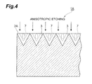
Fig. 4 ] is a sectional view illustrating a second step in the method for manufacturing a light-absorbing substrate in accordance with the embodiment of the present invention; - [
Fig. 5 ] is a plan view illustrating the second step in the method for manufacturing a light-absorbing substrate in accordance with the embodiment of the present invention; - [
Fig. 6 ] is a sectional view illustrating the second step in the method for manufacturing a light-absorbing substrate in accordance with another embodiment of the present invention; - [
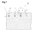
Fig. 7 ] is a sectional view illustrating the first step in the method for manufacturing a light-absorbing substrate in accordance with still another embodiment of the present invention; - [
Fig. 8 ] is a sectional view illustrating the first step in the method for manufacturing a light-absorbing substrate in accordance with the above-mentioned embodiment of the present invention; - [
Fig. 9 ] is a sectional view illustrating the second step in the method for manufacturing a light-absorbing substrate in accordance with the above-mentioned embodiment of the present invention; - [
Fig. 10 ] is a perspective view of a mold manufactured by the method for manufacturing a mold in accordance with an embodiment of the present invention; - [
Fig. 11 ] is a perspective view illustrating a third step in the method for manufacturing a mold in accordance with the embodiment of the present invention; - [
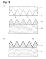
Fig. 12 ] is a sectional view illustrating the third step in the method for manufacturing a mold in accordance with the embodiment of the present invention; and - [
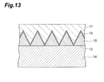
Fig. 13 ] is a sectional view illustrating the third step in the method for manufacturing a mold in accordance with the embodiment of the present invention. - In the following, preferred embodiments of the present invention will be explained in detail with reference to the drawings. In the drawings, the same or equivalent parts will be referred to with the same signs while omitting their overlapping descriptions.
- As illustrated in
Fig. 1 , a light-absorbingsubstrate 1 has asurface 2 with depressions and projections (having an average difference in height of about 10 µm). The light-absorbingsubstrate 1, which is employed in a solar battery, is constituted by a rectangular sheet-like monocrystal silicon substrate whosesurface 2 is a (100) plane. Thesurface 2 is a so-called nonreflective surface and serves as a surface for receiving sunlight. Thesurface 2 is formed with a plurality ofdepressions 3 arranged in a two-dimensional matrix and aflat part 4. Eachdepression 3 is formed into a quadrangular pyramid which becomes wider toward the outside (toward the opening). Theflat part 4 is a part where wiring electrodes for the solar battery and the like are formed. - A method for manufacturing thus constructed light-absorbing
substrate 1 will now be explained. First, as illustrated inFigs. 2 and3 , asubstrate 1A which is a base material for the light-absorbingsubstrate 1 is prepared. Thesubstrate 1A is made of a rectangular sheet-like monocrystal substrate whosesurface 2A is a (100) plane. Subsequently, scheduledformation positions 5 for modifiedregions 7 are set in thesubstrate 1A such as to correspond to the respective center positions of thedepressions 3 of the light-absorbingsubstrate 1 as seen in its thickness direction. Each scheduledformation position 5 is set within thesubstrate 1A at a predetermined distance from thesurface 2A such that at least one of each modifiedregion 7 and a fracture generated from the modifiedregion 7 reaches thesurface 2A. The interval between the adjacent scheduledformation positions 5 is about 10 µm. - Next, the
substrate 1A is irradiated with a laser light L while locating a converging point P at each scheduledformation position 5. This forms a plurality of modifiedregions 7 arranged in a two-dimensional matrix along thesurface 2A within thesubstrate 1A and causes at least one of each modifiedregion 7 and a fracture generated from the modifiedregion 7 to reach thesurface 2A. - Here, when forming the modified
regions 7, thesubstrate 1A is irradiated with the pulsed laser light L having a wavelength of 1064 nm under conditions with a peak power density of 1 × 101 W/cm2 or more at the converging point P and a pulse width of 1 µs or less while using thesurface 2A of thesubstrate 1 as a laser light entrance surface and locating the converging point within thesubstrate 1A. As a consequence, the laser light L is transmitted through thesurface 2A of thesubstrate 1A and absorbed in particular in the vicinity of the scheduled formation positions 5 (i.e., positions of the converging point P where the laser light L is converged) within thesubstrate 1A, whereby the modifiedregions 7 are formed within thesubstrate 1A. Thus, the internal absorption type laser processing forming the modifiedregions 7 within thesubstrate 1A is much different from surface absorption type laser processing which melts or evaporates a part of thesubstrate 1A on thesurface 2A so as to form depressions, grooves, and the like on thesurface 2A. - The modified
regions 7 are regions whose physical characteristics such as density, refractive index, and mechanical strength have attained states different from those of their surroundings. Examples of the modifiedregions 7 include molten processed regions, crack regions, dielectric breakdown regions, refractive index changed regions, and their mixed regions according to the material of thesubstrate 1A. Further examples of the modifiedregions 7 include, according to the material of thesubstrate 1A, an area whose density has changed from that of an unmodified region in a material of a workpiece and an area formed with a lattice defect (which may collectively be referred to as a high-density transitional region). - The molten processed regions, refractive index changed regions, areas where the modified
region 7 has a density different from that of the unmodified region, or areas formed with a lattice defect may further incorporate a fracture (cut or microcrack) therewithin or at an interface between the modifiedregion 7 and an unmodified region. The incorporated fracture may be formed over the whole surface of the modifiedregion 7 or in only a part or a plurality of parts thereof. Molten processed regions are mainly formed as the modifiedregions 7 here, since monocrystal silicon is employed as a material for thesubstrate 1A, though various materials can be selected without being restricted to monocrystal silicon. - During the irradiation, the laser light L is relatively moved along the
surface 2A of thesubstrate 1A so as to follow the direction of polarization of the laser light L which is a linearly-polarized light. The laser light L is pulse-oscillated in the vicinity of each scheduledformation position 5 so as to yield a peak power density at a processing threshold or higher, but continuously oscillated in the remaining parts. This forms the modified region at each scheduledformation position 5 and causes at least one of each modifiedregion 7 and a fracture generated from the modified region to reach thesurface 2A. Each modifiedregion 7 includes at least one modified spot (a modified part formed by irradiation with one pulse of the pulsed laser light L). When one modifiedregion 7 includes a plurality of modified spots, the plurality of modified spots may be formed either continuously or intermittently, though it will be preferred if at least fractures join with each other between the plurality of modified spots. - After forming the modified
regions 7, thesurface 2A of thesubstrate 1A is etched as illustrated inFigs. 4 and5 , so as to produce depressions and projections on thesurface 2A. Here, KOH (potassium hydroxide), for example, is selected as an etchant, with which anisotropic etching is performed. By this time, at least one of each modifiedregion 7 and a fracture generated from the modifiedregion 7 has reached thesurface 2A, so that the etchant enters the modifiedregion 7, whereby the etching selectively progresses from the modifiedregion 7 having a higher etching rate than in its surroundings and acting as a start point. The etching encompasses a case where thesubstrate 1A is immersed in the etchant (dipping) and a case where thesubstrate 1A is coated with the etchant while being rotated (spin etching). - The etching is terminated at a stage where the
surface 2A has attained a desirable form. This anisotropic etching exposes (111) planes having a lower etching rate, so as to formdepressions 3 each shaped like a quadrangular pyramid which becomes wider toward the outside (toward the opening). The foregoing makes thesurface 2A of thesubstrate 1A become thesurface 2 of the light-absorbingsubstrate 1, thereby yielding the light-absorbingsubstrate 1 having thesurface 2 with depressions and projections. - In the method for manufacturing the light-absorbing
substrate 1, as explained in the foregoing, at least one of each modifiedregion 7 and a fracture generated from the modifiedregion 7 reaches thesurface 2A of thesubstrate 1A, so that the etching progresses selectively from the modifiedregion 7 acting as a start point, thereby forming a plurality ofdepressions 3 on thesurface 2A of thesubstrate 1A. Here, positions of the modified regions, i.e., positions of thedepressions 3, can be controlled easily and accurately according to irradiation conditions of the laser light L (e.g., positions at which the converging point P is located, the relative moving speed of the laser light L, the repetition frequency of the laser light L, and timings for smiting the processing threshold of the laser light L). Forms of thedepressions 3 can be controlled easily and precisely according to etching conditions (e.g., etching time and a temperature at which the etchant is used). Therefore, the method for manufacturing the light-absorbingsubstrate 1 can easily manufacture the light-absorbingsubstrate 1 having thesurface 2 with depressions and projections formed in a desirable pattern. - During the irradiation, the laser light L is relatively moved along the
surface 2A of thesubstrate 1A so as to follow the direction of polarization of the laser light L. As a consequence, the modifiedregions 7, fractures generated from the modifiedregions 7, and thermally influenced regions about the modifiedregions 7 are stabilized among a plurality of scheduled formation positions 5. This can inhibit a plurality ofdepressions 3 produced on thesurface 2A of thesubstrate 1A from fluctuating their forms among them. - Anisotropically etching the
surface 2A of thesubstrate 1A as the etching also contributes to inhibiting a plurality ofdepressions 3 from fluctuating their forms among them. Here, since thesubstrate 1A is made of a monocrystal silicon substrate and has thesurface 2A in a (100) plane, (111) planes are exposed as the etching progresses from the modifiedregions 7 acting as a start point, whereby a plurality ofdepressions 3 each shaped like a quadrangular pyramid expanding outward are formed. - As illustrated in
Fig. 6 , isotropic etching may further be performed after the anisotropic etching. This can smoothen theinner faces 3a of the plurality ofdepressions 3 formed on thesurface 2A of thesubstrate 1A. Here, the inner faces 3a of thedepressions 3 each shaped like a quadrangular pyramid expanding outward are smoothened, so as to yield thedepressions 3 each having a form similar to a Winston cone which is highly effective in gathering light. - As illustrated in
Figs. 7 and8 , scheduledformation positions 5 may be set at a plurality of positions differently distanced from thesurface 2A of thesubstrate 1A so as to align along the thickness direction of thesubstrate 1A, and the respective modifiedregions 7 may be formed at the scheduled formation positions 5. That is, the irradiation with the laser light L may be performed a plurality of times while changing the distance from thesurface 2A of thesubstrate 1A to the converging point P of the laser light L, so as to form the respective modifiedregions 7. This makes it possible to form adepression 3 whose ratio of the depth to the width of its opening is greater (e.g., having an aspect ratio of 2 or more) by etching as illustrated inFig. 9 . Preferably, in this case, the scheduledformation positions 5 are irradiated with the laser light L in descending order of their distance from the laser light entrance surface. This aims to prevent a modifiedregion 7 from being formed in front of a scheduledformation position 5 in the advancing direction of the laser light L and inhibiting the conversion of the laser light L. Furthermore, by using the elongate converging point P which extends longer in the thickness direction of thesubstrate 1A (i.e., in the converging point P, the thickness direction of thesubstrate 1A is the longitudinal direction), a elongate modifiedregion 7 which extends longer in the thickness direction of thesubstrate 1A may also be formed. In this case, it is possible to reduce the number of times the laser light L is irradiated. The elongate converging point P can be formed, for example, by aligning a plurality of converging points P in the thickness direction of thesubstrate 1A. - As illustrated in
Fig. 10 , amold 10 has asurface 12 with depressions and projections. Themold 10 is a mold for making a light-absorbing substrate having a surface with depressions and projections (corresponding to the above-mentioned light-absorbing substrate 1) by nanoimprinting or the like and is made of a metal such as nickel, for example. The depressions and projections on thesurface 12 are complementary to those formed on the surface of the light-absorbing substrate. A plurality ofdepressions 13 arranged in a two-dimensional matrix are formed on thesurface 12. Eachdepression 13 is formed into a quadrangular pyramid which becomes thinner toward the inside (toward the side opposite to the opening). - A method for manufacturing thus constructed
mold 10 will now be explained. First, the above-mentioned light-absorbingsubstrate 1 is prepared by the manufacturing method explained above as a master for a light-absorbing substrate to be produced by nanoimprinting or the like. Subsequently, as illustrated inFig. 11(a) , a resistlayer 15 is mounted on asubstrate 14 made of silicon, for example. Then, as illustrated inFig. 11(b) , thesurface 2 of the light-absorbingsubstrate 1 is pressed against the resistlayer 15, so as to transfer the form of thesurface 2 to the resistlayer 15. - Next, as illustrated in
Fig. 12(a) , the light-absorbingsubstrate 1 is released from the resistlayer 15. Subsequently, as illustrated inFig. 12(b) , a metal such as nickel, for example, is vapor-deposited on the surface of the resistlayer 15 formed with depressions and projections complementary to those formed on thesurface 2 of the light-absorbingsubstrate 1, so as to form ametal layer 16. Then, as illustrated inFig. 13 , a metal such as nickel is thickly deposited into a block on themetal layer 16 by electrocasting, so as to form ametal layer 17. Thereafter, the resistlayer 15 is melted away (thesubstrate 14 may also be melted away if necessary), so as to take out the metal layers 16, 17, thereby yielding themold 10. - As explained in the foregoing, the method for manufacturing the
mold 10 prepares the above-mentioned light-absorbingsubstrate 1 by the above-mentioned manufacturing method as a master for the light-absorbing substrate to be made. In the above-mentioned manufacturing method, at least one of each modifiedregion 7 and a fracture generated from the modifiedregion 7 has reached thesurface 2A of thesubstrate 1A, so that the etching selectively progresses from the modifiedregion 7 acting as a start point, thereby forming a plurality ofdepressions 3 on thesurface 2A of thesubstrate 1A. Here, positions of the modified regions, i.e., positions of thedepressions 3, can be controlled easily and accurately according to irradiation conditions of the laser light L. Forms of thedepressions 3 can be controlled easily and precisely according to etching conditions. Since the form of thesurface 2 in which the positions and forms of thedepressions 3 are thus controlled is transferred, themold 10 formed with the depressions and projections complementary to those formed on thesurface 2 is obtained. Hence, the method for manufacturing themold 10 can make themold 10 that can produce a light-absorbing substrate having a surface with depressions and projections formed in a desirable pattern. - Though embodiments of the present invention have been explained in the foregoing, the present invention is not limited to the above-mentioned embodiments. For example, while the above-mentioned embodiments form a plurality of modified
regions 7 within thesubstrate 1A arranged in a two-dimensional matrix along thesurface 2A of thesubstrate 1A, the arrangement of modifiedregions 7 is not limited to matrix forms. A plurality of modifiedregions 7 may be formed in a desirable two-dimensional arrangement so as to produce depressions and projections in a desirable pattern. - The laser light L is not limited to the linearly-polarized light. When the laser light L is polarized, the laser light L which is an elliptically-polarized light having an ellipticity other than 1 can be used. Here, the ellipticity of the elliptically-polarized light is (half the length of the minor axis)/(half the length of the major axis) in the ellipse representing the elliptically-polarized light. Therefore, an elliptically-polarized light with an ellipticity of 1 corresponds to a circularly-polarized light, while an elliptically-polarized light with an ellipticity of 0 (zero) corresponds to a linearly-polarized light. The direction of polarization of the laser light is the direction of the major axis of the ellipse representing the elliptically-polarized light. Hence, when the ellipticity is 0, the direction of polarization of the laser light is the direction of a line representing the linearly-polarized light.
- When the laser light L which is the elliptically-polarized light having an ellipticity other than 1 is used, it is desirable that the direction of polarization of the laser light L and the direction of relative movement of the laser light L substantially coincide with each other (i.e., be substantially parallel to each other). However, fluctuations of forms among a plurality of
depressions 3 can be suppressed more when the angle between the direction of polarization of the laser light L and the direction of relative movement of the laser light L is less than 45° than when the angle is 90°, for example. - Finally, examples of the relationship between the material for the
substrate 1A and an etchant used therefor will be explained. When the material for thesubstrate 1A is Si, a mixed liquid of HNO3 (nitric acid), HF (hydrofluoric acid), and H2O (water) or CH3COOH (acetic acid) can be used as an isotropic etchant. When the material for thesubstrate 1A is Si, KOH (potassium hydroxide), TMAH (aqueous tetramethylammonium hydroxide solution), EDP, NaOH, CsOH, NH4OH, or hydrazine can be used as an anisotropic etchant. - When the material for the
substrate 1A is GaAs, a mixed liquid of H2SO4 (sulfuric acid), H2O2 (hydrogen peroxide solution), and H2O (water); a mixed liquid of H3PO4 (phosphoric acid), H2O2 (hydrogen peroxide solution), and H2O (water); HNO3 (nitric acid); HCl (hydrochloric acid); CH3OH (bromomethane); or a mixed liquid of NH4OH (ammonium hydroxide), H2O2 (hydrogen peroxide solution), and H2O (water) can be used. When the material for thesubstrate 1A is silica (glass), a mixed liquid of HF (hydrofluoric acid) and H2O (water); HF; or NH4F (saturated aqueous solution of ammonium bifluoride) can be used. When the material for thesubstrate 1A is sapphire, H3PO4 (phosphoric acid) or H2SO4 (sulfuric acid) + H3PO4 (phosphoric acid) can be used. When the material for thesubstrate 1A is SiC, KOH (potassium hydroxide) can be used. When the material for thesubstrate 1A is quartz, NH4F can be used. - The present invention can provide a method for manufacturing a light-absorbing substrate which can easily manufacture a light-absorbing substrate having a surface with depressions and projections formed in a desirable pattern, and a mold for making the same.
- 1...light-absorbing substrate; 1A... substrate; 2... surface; 2A...surface; 7...modified region; 10...mold; L...laser light
Claims (6)
- A method for manufacturing a light-absorbing substrate having a surface with depressions and projections, the method comprising:a first step of irradiating a substrate with a laser light so as to form a plurality of modified regions arranged two-dimensionally along a surface of the substrate within the substrate and cause at least one of each modified region and a fracture generated from the modified region to reach the surface of the substrate; anda second step of etching the surface of the substrate after the first step so as to form depressions and projections on the surface of the substrate.
- A method for manufacturing a light-absorbing substrate according to claim 1, wherein, in the second step, anisotropic etching is performed as the etching.
- A method for manufacturing a light-absorbing substrate according to claim 2, wherein, in the second step, isotropic etching is performed as the etching after the anisotropic etching.
- A method for manufacturing a light-absorbing substrate according to one of claims 1 to 3, wherein, in the first step, the laser light is relatively moved along the surface of the substrate so as to follow a direction of polarization of the laser light.
- A method for manufacturing a light-absorbing substrate according to one of claims 1 to 4, wherein, in the first step, the substrate is irradiated with the laser light a plurality of times while changing the distance between the surface of the substrate and a converging point of the laser light so as to form the respective modified regions.
- A method for manufacturing a mold for making a light-absorbing substrate having a surface with depressions and projections, the method comprising:a first step of irradiating a substrate with a laser light so as to form a plurality of modified regions arranged two-dimensionally along a surface of the substrate within the substrate and cause at least one of each modified region and a fracture generated from the modified region to reach the surface of the substrate;a second step of etching the surface of the substrate after the first step so as to form depressions and projections on the surface of the substrate; anda third step of transferring a form of the surface of the substrate after the second step so as to yield the mold.
Applications Claiming Priority (2)
| Application Number | Priority Date | Filing Date | Title |
|---|---|---|---|
| JP2010167443 | 2010-07-26 | ||
| PCT/JP2011/066358 WO2012014723A1 (en) | 2010-07-26 | 2011-07-19 | Method for manufacturing light-absorbing substrate and method for manufacturing die for manufacturing light-absorbing substrate |
Publications (3)
| Publication Number | Publication Date |
|---|---|
| EP2600411A1 true EP2600411A1 (en) | 2013-06-05 |
| EP2600411A4 EP2600411A4 (en) | 2017-01-04 |
| EP2600411B1 EP2600411B1 (en) | 2019-08-21 |
Family
ID=45529939
Family Applications (1)
| Application Number | Title | Priority Date | Filing Date |
|---|---|---|---|
| EP11812315.7A Active EP2600411B1 (en) | 2010-07-26 | 2011-07-19 | Method for manufacturing light-absorbing substrate and method for manufacturing die for manufacturing light-absorbing substrate |
Country Status (7)
| Country | Link |
|---|---|
| US (1) | US9108269B2 (en) |
| EP (1) | EP2600411B1 (en) |
| JP (1) | JP5508533B2 (en) |
| KR (1) | KR101825238B1 (en) |
| CN (1) | CN103026497B (en) |
| TW (1) | TWI549307B (en) |
| WO (1) | WO2012014723A1 (en) |
Cited By (2)
| Publication number | Priority date | Publication date | Assignee | Title |
|---|---|---|---|---|
| EP2599582A4 (en) * | 2010-07-26 | 2017-01-04 | Hamamatsu Photonics K.K. | Substrate processing method |
| DE102020114195A1 (en) | 2020-05-27 | 2021-12-02 | Lpkf Laser & Electronics Aktiengesellschaft | Method for making a recess in a substrate |
Families Citing this family (7)
| Publication number | Priority date | Publication date | Assignee | Title |
|---|---|---|---|---|
| JP2015130367A (en) * | 2012-04-24 | 2015-07-16 | 三菱電機株式会社 | Solar cell and manufacturing method therefor |
| JP2013251456A (en) * | 2012-06-01 | 2013-12-12 | Denso Corp | Semiconductor device manufacturing method and semiconductor device |
| US9814099B2 (en) * | 2013-08-02 | 2017-11-07 | Applied Materials, Inc. | Substrate support with surface feature for reduced reflection and manufacturing techniques for producing same |
| EP4061101A1 (en) | 2014-09-16 | 2022-09-21 | LPKF Laser & Electronics AG | Method for creating at least one recess or opening in a plate-shaped workpiece |
| DE102015000451A1 (en) * | 2015-01-15 | 2016-07-21 | Siltectra Gmbh | Uneven Wafer and Method of Making an Uneven Wafer |
| CN114566556A (en) * | 2022-02-28 | 2022-05-31 | 安徽华晟新能源科技有限公司 | Processing method of semiconductor substrate layer, solar cell and preparation method of solar cell |
| KR102710865B1 (en) | 2023-01-13 | 2024-09-30 | 한국과학기술연구원 | Laser processing appartus and method for texturing solar cell substrate using the same |
Family Cites Families (78)
| Publication number | Priority date | Publication date | Assignee | Title |
|---|---|---|---|---|
| US4325182A (en) * | 1980-08-25 | 1982-04-20 | General Electric Company | Fast isolation diffusion |
| JPS59127878A (en) * | 1983-01-12 | 1984-07-23 | Semiconductor Energy Lab Co Ltd | Manufacture of photoelectric conversion device |
| US4626613A (en) * | 1983-12-23 | 1986-12-02 | Unisearch Limited | Laser grooved solar cell |
| JPS63317270A (en) * | 1987-06-18 | 1988-12-26 | Komatsu Ltd | Laser processing equipment |
| AU612226B2 (en) * | 1987-12-17 | 1991-07-04 | Unisearch Limited | Solar cells with tilted geometrical features |
| US5081049A (en) * | 1988-07-18 | 1992-01-14 | Unisearch Limited | Sculpted solar cell surfaces |
| US5322988A (en) * | 1990-03-29 | 1994-06-21 | The United States Of America As Represented By The Secretary Of The Navy | Laser texturing |
| US5164324A (en) * | 1990-03-29 | 1992-11-17 | The United States Of America As Represented By The Secretary Of The Navy | Laser texturing |
| JPH04150212A (en) | 1990-10-09 | 1992-05-22 | Seiko Epson Corp | Etching method for crystal substrate |
| JPH04339586A (en) * | 1991-05-13 | 1992-11-26 | Mitsubishi Electric Corp | Laser beam machine |
| JP2873937B2 (en) | 1996-05-24 | 1999-03-24 | 工業技術院長 | Optical microfabrication method for glass |
| US6162658A (en) * | 1996-10-14 | 2000-12-19 | Unisearch Limited | Metallization of buried contact solar cells |
| JP3271990B2 (en) | 1997-03-21 | 2002-04-08 | 三洋電機株式会社 | Photovoltaic device and method for manufacturing the same |
| JP4473349B2 (en) * | 1997-06-30 | 2010-06-02 | マクス−プランク−ゲゼルシャフト ツル フォルデルング デル ヴァイセンシャフト エー ファウ | Layered structure manufacturing method and semiconductor substrate |
| JP3490297B2 (en) * | 1998-06-30 | 2004-01-26 | 株式会社東芝 | Polycrystalline semiconductor device and method of manufacturing the same |
| JP2001015786A (en) * | 1999-07-02 | 2001-01-19 | Kanegafuchi Chem Ind Co Ltd | Laser scribe method for fabrication of integrated thin-film solar cells |
| JP3732993B2 (en) | 2000-02-09 | 2006-01-11 | シャープ株式会社 | Solar cell and manufacturing method thereof |
| JP4659300B2 (en) | 2000-09-13 | 2011-03-30 | 浜松ホトニクス株式会社 | Laser processing method and semiconductor chip manufacturing method |
| JP4880820B2 (en) | 2001-01-19 | 2012-02-22 | 株式会社レーザーシステム | Laser assisted machining method |
| US7442629B2 (en) * | 2004-09-24 | 2008-10-28 | President & Fellows Of Harvard College | Femtosecond laser-induced formation of submicrometer spikes on a semiconductor substrate |
| US7057256B2 (en) * | 2001-05-25 | 2006-06-06 | President & Fellows Of Harvard College | Silicon-based visible and near-infrared optoelectric devices |
| US7354792B2 (en) * | 2001-05-25 | 2008-04-08 | President And Fellows Of Harvard College | Manufacture of silicon-based devices having disordered sulfur-doped surface layers |
| US6754429B2 (en) * | 2001-07-06 | 2004-06-22 | Corning Incorporated | Method of making optical fiber devices and devices thereof |
| JP2003258285A (en) * | 2002-02-27 | 2003-09-12 | Sharp Corp | Method for producing surface uneven structure and solar cell |
| AU2003211763A1 (en) | 2002-03-12 | 2003-09-22 | Hamamatsu Photonics K.K. | Method for dicing substrate |
| CA2428187C (en) * | 2002-05-08 | 2012-10-02 | National Research Council Of Canada | Method of fabricating sub-micron structures in transparent dielectric materials |
| JP2004047776A (en) | 2002-07-12 | 2004-02-12 | Honda Motor Co Ltd | Solar cell and method of manufacturing the same |
| JP4329374B2 (en) | 2002-07-29 | 2009-09-09 | パナソニック電工株式会社 | LIGHT EMITTING ELEMENT AND MANUFACTURING METHOD THEREOF |
| JP4158481B2 (en) | 2002-10-21 | 2008-10-01 | セイコーエプソン株式会社 | Laser processing method and apparatus, and drilling method using the apparatus |
| JP2004160618A (en) | 2002-11-15 | 2004-06-10 | Seiko Epson Corp | Micromachine and method of manufacturing micromachine |
| JP2004223586A (en) | 2003-01-24 | 2004-08-12 | Institute Of Physical & Chemical Research | Processing method inside transparent material |
| JP2004304130A (en) | 2003-04-01 | 2004-10-28 | Seiko Epson Corp | Method for manufacturing semiconductor device |
| JP2004351494A (en) | 2003-05-30 | 2004-12-16 | Seiko Epson Corp | Drilling method of material transparent to laser |
| JP2004359475A (en) | 2003-06-02 | 2004-12-24 | Seiko Epson Corp | Method for manufacturing optical element and optical device |
| JP4182841B2 (en) | 2003-08-28 | 2008-11-19 | セイコーエプソン株式会社 | Single crystal substrate processing method |
| JP2005121916A (en) | 2003-10-16 | 2005-05-12 | Seiko Epson Corp | Method for manufacturing substrate with recess for lenticular lens, substrate with recess for lenticular lens, lenticular lens substrate, transmissive screen and rear projector |
| JP2005121915A (en) | 2003-10-16 | 2005-05-12 | Seiko Epson Corp | Manufacturing method of substrate with recess for microlens, substrate with recess for microlens, microlens substrate, counter substrate for liquid crystal panel, liquid crystal panel, and projection display device |
| JP2005144586A (en) | 2003-11-13 | 2005-06-09 | Seiko Epson Corp | Structure manufacturing method, droplet discharge head, and droplet discharge apparatus |
| JP2005144622A (en) | 2003-11-18 | 2005-06-09 | Seiko Epson Corp | Structure manufacturing method, droplet discharge head, and droplet discharge apparatus |
| JP2005152693A (en) | 2003-11-20 | 2005-06-16 | Seiko Epson Corp | Method for manufacturing structure body, liquid drop delivery head and liquid drop delivery device |
| JP2005208175A (en) | 2004-01-20 | 2005-08-04 | Seiko Epson Corp | OPTICAL COMPONENT AND METHOD FOR MANUFACTURING THE SAME, OPTICAL MODULE, OPTICAL COMMUNICATION DEVICE, ELECTRONIC DEVICE |
| JP2005206401A (en) | 2004-01-21 | 2005-08-04 | Seiko Epson Corp | Structure manufacturing method, droplet discharge head, and droplet discharge apparatus |
| JP2005306702A (en) | 2004-04-26 | 2005-11-04 | Namiki Precision Jewel Co Ltd | Method for forming a microhole having a tapered shape |
| JP2005351774A (en) | 2004-06-10 | 2005-12-22 | Seiko Epson Corp | Microarray manufacturing head manufacturing method, microarray manufacturing head, and microarray manufacturing apparatus |
| JP4630971B2 (en) | 2004-12-21 | 2011-02-09 | 並木精密宝石株式会社 | Microstructure formation method using pulsed laser |
| JP4468191B2 (en) * | 2005-01-27 | 2010-05-26 | 株式会社日立製作所 | Metal structure and manufacturing method thereof |
| JP2006290630A (en) | 2005-02-23 | 2006-10-26 | Nippon Sheet Glass Co Ltd | Processing method of glass using laser |
| US7438824B2 (en) * | 2005-03-25 | 2008-10-21 | National Research Council Of Canada | Fabrication of long range periodic nanostructures in transparent or semitransparent dielectrics |
| JP2007036758A (en) | 2005-07-27 | 2007-02-08 | Seiko Epson Corp | AT-cut crystal resonator element, method for manufacturing the same, and crystal device |
| JP2007101833A (en) | 2005-10-04 | 2007-04-19 | Seiko Epson Corp | Microlens manufacturing method, microlens, spatial light modulator, screen and projector |
| JP4708428B2 (en) * | 2005-11-22 | 2011-06-22 | オリンパス株式会社 | Processing method of glass substrate |
| DE102006042617B4 (en) * | 2006-09-05 | 2010-04-08 | Q-Cells Se | Method for generating local contacts |
| JP2008147412A (en) | 2006-12-11 | 2008-06-26 | Matsushita Electric Ind Co Ltd | Semiconductor wafer, semiconductor device, semiconductor wafer manufacturing method, and semiconductor device manufacturing method |
| TWI432592B (en) * | 2007-04-27 | 2014-04-01 | Honeywell Int Inc | Sputtering targets having reduced burn-in time, their methods of production and uses thereof |
| WO2008146744A1 (en) | 2007-05-25 | 2008-12-04 | Hamamatsu Photonics K.K. | Working method for cutting |
| JP4808271B2 (en) * | 2007-07-31 | 2011-11-02 | 三菱電機株式会社 | Method for manufacturing photovoltaic device |
| JP5527956B2 (en) * | 2007-10-10 | 2014-06-25 | 株式会社半導体エネルギー研究所 | Manufacturing method of semiconductor substrate |
| JP2009277979A (en) * | 2008-05-16 | 2009-11-26 | Mitsubishi Electric Corp | Method for roughening substrate, photovoltaic device, and method for manufacturing the same |
| US8257603B2 (en) * | 2008-08-29 | 2012-09-04 | Corning Incorporated | Laser patterning of glass bodies |
| JP5191866B2 (en) * | 2008-11-12 | 2013-05-08 | スタンレー電気株式会社 | Semiconductor light emitting device manufacturing method and semiconductor light emitting device |
| EP2371006A4 (en) * | 2008-11-26 | 2013-05-01 | Solexel Inc | TRUNCATED PYRAMID STRUCTURES FOR TRANSPARENT SOLAR CELLS |
| US8652869B2 (en) * | 2009-03-25 | 2014-02-18 | Mitsubishi Electric Corporation | Method for roughening substrate surface and method for manufacturing photovoltaic device |
| MY159405A (en) * | 2009-05-29 | 2016-12-30 | Solexel Inc | Three-dimensional thin-film semiconductor substrate with through-holes and methods of manufacturing |
| WO2011004556A1 (en) * | 2009-07-06 | 2011-01-13 | 株式会社フジクラ | Through-wiring board and method of manufacturing same |
| JP2011053495A (en) * | 2009-09-02 | 2011-03-17 | Sony Corp | Optical element and method for producing the same |
| EP2493273A4 (en) * | 2009-10-23 | 2013-10-16 | Fujikura Ltd | STRUCTURE AND METHOD FOR MOUNTING DEVICE |
| WO2011048858A1 (en) * | 2009-10-23 | 2011-04-28 | 株式会社フジクラ | Device mounting structure and device mounting method |
| KR20110082372A (en) * | 2010-01-11 | 2011-07-19 | 삼성전자주식회사 | Solar cell module and manufacturing method thereof |
| CN102741012B (en) * | 2010-02-05 | 2014-12-24 | 株式会社藤仓 | Formation method of fine structure and matrix having fine structure |
| JP2011218398A (en) * | 2010-04-08 | 2011-11-04 | Fujikura Ltd | Method for forming microstructure, laser irradiation device, and substrate |
| JP5513227B2 (en) * | 2010-04-08 | 2014-06-04 | 株式会社フジクラ | Fine structure forming method, laser irradiation apparatus, and substrate |
| WO2011140273A2 (en) * | 2010-05-04 | 2011-11-10 | Sionyx, Inc. | Photovoltaic devices and associated methods |
| TW201145546A (en) * | 2010-06-15 | 2011-12-16 | An Ching New Energy Machinery & Equipment Co Ltd | Solar cell structure with high electro-optic conversion efficiency and manufacturing method thereof |
| WO2012017857A1 (en) * | 2010-08-05 | 2012-02-09 | 株式会社フジクラ | Electronic circuit chip and method of manufacturing electronic circuit chip |
| US8512588B2 (en) * | 2010-08-13 | 2013-08-20 | Lawrence Livermore National Security, Llc | Method of fabricating a scalable nanoporous membrane filter |
| US8703517B2 (en) * | 2010-10-29 | 2014-04-22 | Denso Corporation | Method of Manufacturing a Semiconductor Device Including Removing a Reformed Layer |
| CN105679862A (en) * | 2010-12-21 | 2016-06-15 | 西奥尼克斯公司 | Semiconductor devices having reduced substrate damage and associated methods |
| TWI480737B (en) * | 2011-12-30 | 2015-04-11 | Pegatron Corp | Device expansion system and method for expanding the same |
-
2011
- 2011-07-19 US US13/388,595 patent/US9108269B2/en not_active Expired - Fee Related
- 2011-07-19 WO PCT/JP2011/066358 patent/WO2012014723A1/en not_active Ceased
- 2011-07-19 EP EP11812315.7A patent/EP2600411B1/en active Active
- 2011-07-19 CN CN201180036889.3A patent/CN103026497B/en not_active Expired - Fee Related
- 2011-07-19 JP JP2012526436A patent/JP5508533B2/en active Active
- 2011-07-19 KR KR1020127031687A patent/KR101825238B1/en not_active Expired - Fee Related
- 2011-07-26 TW TW100126372A patent/TWI549307B/en not_active IP Right Cessation
Cited By (3)
| Publication number | Priority date | Publication date | Assignee | Title |
|---|---|---|---|---|
| EP2599582A4 (en) * | 2010-07-26 | 2017-01-04 | Hamamatsu Photonics K.K. | Substrate processing method |
| DE102020114195A1 (en) | 2020-05-27 | 2021-12-02 | Lpkf Laser & Electronics Aktiengesellschaft | Method for making a recess in a substrate |
| WO2021239302A1 (en) | 2020-05-27 | 2021-12-02 | Lpkf Laser & Electronics Ag | Method for introducing a recess into a substrate |
Also Published As
| Publication number | Publication date |
|---|---|
| KR20130098167A (en) | 2013-09-04 |
| US9108269B2 (en) | 2015-08-18 |
| JPWO2012014723A1 (en) | 2013-09-12 |
| KR101825238B1 (en) | 2018-02-02 |
| TWI549307B (en) | 2016-09-11 |
| WO2012014723A1 (en) | 2012-02-02 |
| EP2600411A4 (en) | 2017-01-04 |
| EP2600411B1 (en) | 2019-08-21 |
| JP5508533B2 (en) | 2014-06-04 |
| CN103026497A (en) | 2013-04-03 |
| CN103026497B (en) | 2016-08-03 |
| US20120125887A1 (en) | 2012-05-24 |
| TW201230348A (en) | 2012-07-16 |
Similar Documents
| Publication | Publication Date | Title |
|---|---|---|
| EP2600411B1 (en) | Method for manufacturing light-absorbing substrate and method for manufacturing die for manufacturing light-absorbing substrate | |
| JP7837643B2 (en) | Silica-containing substrate with vias having axially variable sidewall taper | |
| JP7320456B2 (en) | Article having vias with geometry attributes and method of making same | |
| EP2599582B1 (en) | Substrate processing method | |
| EP3510002B1 (en) | Articles having holes with morphology attributes and methods for fabricating the same | |
| CN106425129B (en) | The method for forming high density hole array in glass | |
| US8961806B2 (en) | Laser processing method | |
| EP2599576B1 (en) | Laser processing method | |
| US20120135608A1 (en) | Substrate processing method | |
| US8466042B2 (en) | Method for manufacturing separated micromechanical components situated on a silicon substrate and components manufactured therefrom | |
| EP2599581B1 (en) | Laser processing method | |
| JP7640090B2 (en) | Laser processing method and device for transparent materials | |
| CN104126153B (en) | Method for manufacturing resonator | |
| EP2190026A1 (en) | Method for manufacturing photovoltaic device | |
| CN117548861B (en) | A method and system for processing slots on light-transmitting materials | |
| JP2021106229A (en) | Glass substrate having through hole and hollow portion and manufacturing method thereof | |
| CN116621463B (en) | A method for forming a hole structure | |
| JP2001291705A (en) | Etching method | |
| KR20030071899A (en) | Method for manufacturing waveguide groove by using the dry etching | |
| Flemming et al. | Cost effective 3D Glass Microfabrication for Advanced Packaging Applications | |
| Byeon et al. | Through-Glass Via (TGV) Fabrication in Quartz and D263 Glass Using Picosecond Laser Processing and Chemical Etching: AComparative Parametric Study | |
| TW202102450A (en) | Method of making through via on glass substrate including the steps of laser processing the glass substrate, immersing the glass substrate in an etching bath, ultrasonic vibrating the etching bath to remove the transformed structure area, and continuously etching | |
| EP2688091A1 (en) | Method for producing a cavity by anisotropically removing material from a substrate |
Legal Events
| Date | Code | Title | Description |
|---|---|---|---|
| PUAI | Public reference made under article 153(3) epc to a published international application that has entered the european phase |
Free format text: ORIGINAL CODE: 0009012 |
|
| 17P | Request for examination filed |
Effective date: 20130222 |
|
| AK | Designated contracting states |
Kind code of ref document: A1 Designated state(s): AL AT BE BG CH CY CZ DE DK EE ES FI FR GB GR HR HU IE IS IT LI LT LU LV MC MK MT NL NO PL PT RO RS SE SI SK SM TR |
|
| DAX | Request for extension of the european patent (deleted) | ||
| RA4 | Supplementary search report drawn up and despatched (corrected) |
Effective date: 20161205 |
|
| RIC1 | Information provided on ipc code assigned before grant |
Ipc: H01L 31/04 20060101AFI20161129BHEP |
|
| GRAP | Despatch of communication of intention to grant a patent |
Free format text: ORIGINAL CODE: EPIDOSNIGR1 |
|
| STAA | Information on the status of an ep patent application or granted ep patent |
Free format text: STATUS: GRANT OF PATENT IS INTENDED |
|
| INTG | Intention to grant announced |
Effective date: 20190319 |
|
| GRAS | Grant fee paid |
Free format text: ORIGINAL CODE: EPIDOSNIGR3 |
|
| GRAA | (expected) grant |
Free format text: ORIGINAL CODE: 0009210 |
|
| STAA | Information on the status of an ep patent application or granted ep patent |
Free format text: STATUS: THE PATENT HAS BEEN GRANTED |
|
| AK | Designated contracting states |
Kind code of ref document: B1 Designated state(s): AL AT BE BG CH CY CZ DE DK EE ES FI FR GB GR HR HU IE IS IT LI LT LU LV MC MK MT NL NO PL PT RO RS SE SI SK SM TR |
|
| REG | Reference to a national code |
Ref country code: GB Ref legal event code: FG4D |
|
| REG | Reference to a national code |
Ref country code: CH Ref legal event code: EP |
|
| REG | Reference to a national code |
Ref country code: DE Ref legal event code: R096 Ref document number: 602011061481 Country of ref document: DE |
|
| REG | Reference to a national code |
Ref country code: AT Ref legal event code: REF Ref document number: 1170738 Country of ref document: AT Kind code of ref document: T Effective date: 20190915 |
|
| REG | Reference to a national code |
Ref country code: IE Ref legal event code: FG4D |
|
| REG | Reference to a national code |
Ref country code: LT Ref legal event code: MG4D |
|
| REG | Reference to a national code |
Ref country code: NL Ref legal event code: MP Effective date: 20190821 |
|
| PG25 | Lapsed in a contracting state [announced via postgrant information from national office to epo] |
Ref country code: PT Free format text: LAPSE BECAUSE OF FAILURE TO SUBMIT A TRANSLATION OF THE DESCRIPTION OR TO PAY THE FEE WITHIN THE PRESCRIBED TIME-LIMIT Effective date: 20191223 Ref country code: SE Free format text: LAPSE BECAUSE OF FAILURE TO SUBMIT A TRANSLATION OF THE DESCRIPTION OR TO PAY THE FEE WITHIN THE PRESCRIBED TIME-LIMIT Effective date: 20190821 Ref country code: LT Free format text: LAPSE BECAUSE OF FAILURE TO SUBMIT A TRANSLATION OF THE DESCRIPTION OR TO PAY THE FEE WITHIN THE PRESCRIBED TIME-LIMIT Effective date: 20190821 Ref country code: HR Free format text: LAPSE BECAUSE OF FAILURE TO SUBMIT A TRANSLATION OF THE DESCRIPTION OR TO PAY THE FEE WITHIN THE PRESCRIBED TIME-LIMIT Effective date: 20190821 Ref country code: FI Free format text: LAPSE BECAUSE OF FAILURE TO SUBMIT A TRANSLATION OF THE DESCRIPTION OR TO PAY THE FEE WITHIN THE PRESCRIBED TIME-LIMIT Effective date: 20190821 Ref country code: BG Free format text: LAPSE BECAUSE OF FAILURE TO SUBMIT A TRANSLATION OF THE DESCRIPTION OR TO PAY THE FEE WITHIN THE PRESCRIBED TIME-LIMIT Effective date: 20191121 Ref country code: NO Free format text: LAPSE BECAUSE OF FAILURE TO SUBMIT A TRANSLATION OF THE DESCRIPTION OR TO PAY THE FEE WITHIN THE PRESCRIBED TIME-LIMIT Effective date: 20191121 Ref country code: NL Free format text: LAPSE BECAUSE OF FAILURE TO SUBMIT A TRANSLATION OF THE DESCRIPTION OR TO PAY THE FEE WITHIN THE PRESCRIBED TIME-LIMIT Effective date: 20190821 |
|
| PG25 | Lapsed in a contracting state [announced via postgrant information from national office to epo] |
Ref country code: AL Free format text: LAPSE BECAUSE OF FAILURE TO SUBMIT A TRANSLATION OF THE DESCRIPTION OR TO PAY THE FEE WITHIN THE PRESCRIBED TIME-LIMIT Effective date: 20190821 Ref country code: LV Free format text: LAPSE BECAUSE OF FAILURE TO SUBMIT A TRANSLATION OF THE DESCRIPTION OR TO PAY THE FEE WITHIN THE PRESCRIBED TIME-LIMIT Effective date: 20190821 Ref country code: ES Free format text: LAPSE BECAUSE OF FAILURE TO SUBMIT A TRANSLATION OF THE DESCRIPTION OR TO PAY THE FEE WITHIN THE PRESCRIBED TIME-LIMIT Effective date: 20190821 Ref country code: RS Free format text: LAPSE BECAUSE OF FAILURE TO SUBMIT A TRANSLATION OF THE DESCRIPTION OR TO PAY THE FEE WITHIN THE PRESCRIBED TIME-LIMIT Effective date: 20190821 Ref country code: GR Free format text: LAPSE BECAUSE OF FAILURE TO SUBMIT A TRANSLATION OF THE DESCRIPTION OR TO PAY THE FEE WITHIN THE PRESCRIBED TIME-LIMIT Effective date: 20191122 Ref country code: IS Free format text: LAPSE BECAUSE OF FAILURE TO SUBMIT A TRANSLATION OF THE DESCRIPTION OR TO PAY THE FEE WITHIN THE PRESCRIBED TIME-LIMIT Effective date: 20191221 |
|
| REG | Reference to a national code |
Ref country code: AT Ref legal event code: MK05 Ref document number: 1170738 Country of ref document: AT Kind code of ref document: T Effective date: 20190821 |
|
| PG25 | Lapsed in a contracting state [announced via postgrant information from national office to epo] |
Ref country code: TR Free format text: LAPSE BECAUSE OF FAILURE TO SUBMIT A TRANSLATION OF THE DESCRIPTION OR TO PAY THE FEE WITHIN THE PRESCRIBED TIME-LIMIT Effective date: 20190821 |
|
| PG25 | Lapsed in a contracting state [announced via postgrant information from national office to epo] |
Ref country code: RO Free format text: LAPSE BECAUSE OF FAILURE TO SUBMIT A TRANSLATION OF THE DESCRIPTION OR TO PAY THE FEE WITHIN THE PRESCRIBED TIME-LIMIT Effective date: 20190821 Ref country code: IT Free format text: LAPSE BECAUSE OF FAILURE TO SUBMIT A TRANSLATION OF THE DESCRIPTION OR TO PAY THE FEE WITHIN THE PRESCRIBED TIME-LIMIT Effective date: 20190821 Ref country code: DK Free format text: LAPSE BECAUSE OF FAILURE TO SUBMIT A TRANSLATION OF THE DESCRIPTION OR TO PAY THE FEE WITHIN THE PRESCRIBED TIME-LIMIT Effective date: 20190821 Ref country code: AT Free format text: LAPSE BECAUSE OF FAILURE TO SUBMIT A TRANSLATION OF THE DESCRIPTION OR TO PAY THE FEE WITHIN THE PRESCRIBED TIME-LIMIT Effective date: 20190821 Ref country code: EE Free format text: LAPSE BECAUSE OF FAILURE TO SUBMIT A TRANSLATION OF THE DESCRIPTION OR TO PAY THE FEE WITHIN THE PRESCRIBED TIME-LIMIT Effective date: 20190821 Ref country code: PL Free format text: LAPSE BECAUSE OF FAILURE TO SUBMIT A TRANSLATION OF THE DESCRIPTION OR TO PAY THE FEE WITHIN THE PRESCRIBED TIME-LIMIT Effective date: 20190821 |
|
| PG25 | Lapsed in a contracting state [announced via postgrant information from national office to epo] |
Ref country code: IS Free format text: LAPSE BECAUSE OF FAILURE TO SUBMIT A TRANSLATION OF THE DESCRIPTION OR TO PAY THE FEE WITHIN THE PRESCRIBED TIME-LIMIT Effective date: 20200224 Ref country code: CZ Free format text: LAPSE BECAUSE OF FAILURE TO SUBMIT A TRANSLATION OF THE DESCRIPTION OR TO PAY THE FEE WITHIN THE PRESCRIBED TIME-LIMIT Effective date: 20190821 Ref country code: SM Free format text: LAPSE BECAUSE OF FAILURE TO SUBMIT A TRANSLATION OF THE DESCRIPTION OR TO PAY THE FEE WITHIN THE PRESCRIBED TIME-LIMIT Effective date: 20190821 Ref country code: SK Free format text: LAPSE BECAUSE OF FAILURE TO SUBMIT A TRANSLATION OF THE DESCRIPTION OR TO PAY THE FEE WITHIN THE PRESCRIBED TIME-LIMIT Effective date: 20190821 |
|
| REG | Reference to a national code |
Ref country code: DE Ref legal event code: R097 Ref document number: 602011061481 Country of ref document: DE |
|
| PLBE | No opposition filed within time limit |
Free format text: ORIGINAL CODE: 0009261 |
|
| STAA | Information on the status of an ep patent application or granted ep patent |
Free format text: STATUS: NO OPPOSITION FILED WITHIN TIME LIMIT |
|
| PG2D | Information on lapse in contracting state deleted |
Ref country code: IS |
|
| 26N | No opposition filed |
Effective date: 20200603 |
|
| PG25 | Lapsed in a contracting state [announced via postgrant information from national office to epo] |
Ref country code: SI Free format text: LAPSE BECAUSE OF FAILURE TO SUBMIT A TRANSLATION OF THE DESCRIPTION OR TO PAY THE FEE WITHIN THE PRESCRIBED TIME-LIMIT Effective date: 20190821 |
|
| REG | Reference to a national code |
Ref country code: DE Ref legal event code: R119 Ref document number: 602011061481 Country of ref document: DE |
|
| PG25 | Lapsed in a contracting state [announced via postgrant information from national office to epo] |
Ref country code: MC Free format text: LAPSE BECAUSE OF FAILURE TO SUBMIT A TRANSLATION OF THE DESCRIPTION OR TO PAY THE FEE WITHIN THE PRESCRIBED TIME-LIMIT Effective date: 20190821 |
|
| REG | Reference to a national code |
Ref country code: CH Ref legal event code: PL |
|
| GBPC | Gb: european patent ceased through non-payment of renewal fee |
Effective date: 20200719 |
|
| REG | Reference to a national code |
Ref country code: BE Ref legal event code: MM Effective date: 20200731 |
|
| PG25 | Lapsed in a contracting state [announced via postgrant information from national office to epo] |
Ref country code: LI Free format text: LAPSE BECAUSE OF NON-PAYMENT OF DUE FEES Effective date: 20200731 Ref country code: CH Free format text: LAPSE BECAUSE OF NON-PAYMENT OF DUE FEES Effective date: 20200731 Ref country code: LU Free format text: LAPSE BECAUSE OF NON-PAYMENT OF DUE FEES Effective date: 20200719 Ref country code: FR Free format text: LAPSE BECAUSE OF NON-PAYMENT OF DUE FEES Effective date: 20200731 Ref country code: GB Free format text: LAPSE BECAUSE OF NON-PAYMENT OF DUE FEES Effective date: 20200719 |
|
| PG25 | Lapsed in a contracting state [announced via postgrant information from national office to epo] |
Ref country code: BE Free format text: LAPSE BECAUSE OF NON-PAYMENT OF DUE FEES Effective date: 20200731 Ref country code: DE Free format text: LAPSE BECAUSE OF NON-PAYMENT OF DUE FEES Effective date: 20210202 |
|
| PG25 | Lapsed in a contracting state [announced via postgrant information from national office to epo] |
Ref country code: IE Free format text: LAPSE BECAUSE OF NON-PAYMENT OF DUE FEES Effective date: 20200719 |
|
| PG25 | Lapsed in a contracting state [announced via postgrant information from national office to epo] |
Ref country code: MT Free format text: LAPSE BECAUSE OF FAILURE TO SUBMIT A TRANSLATION OF THE DESCRIPTION OR TO PAY THE FEE WITHIN THE PRESCRIBED TIME-LIMIT Effective date: 20190821 Ref country code: CY Free format text: LAPSE BECAUSE OF FAILURE TO SUBMIT A TRANSLATION OF THE DESCRIPTION OR TO PAY THE FEE WITHIN THE PRESCRIBED TIME-LIMIT Effective date: 20190821 |
|
| PG25 | Lapsed in a contracting state [announced via postgrant information from national office to epo] |
Ref country code: MK Free format text: LAPSE BECAUSE OF FAILURE TO SUBMIT A TRANSLATION OF THE DESCRIPTION OR TO PAY THE FEE WITHIN THE PRESCRIBED TIME-LIMIT Effective date: 20190821 |