EP4061101A1 - Method for creating at least one recess or opening in a plate-shaped workpiece - Google Patents
Method for creating at least one recess or opening in a plate-shaped workpiece Download PDFInfo
- Publication number
- EP4061101A1 EP4061101A1 EP22167179.5A EP22167179A EP4061101A1 EP 4061101 A1 EP4061101 A1 EP 4061101A1 EP 22167179 A EP22167179 A EP 22167179A EP 4061101 A1 EP4061101 A1 EP 4061101A1
- Authority
- EP
- European Patent Office
- Prior art keywords
- workpiece
- cross
- constrictions
- recess
- sectional
- Prior art date
- Legal status (The legal status is an assumption and is not a legal conclusion. Google has not performed a legal analysis and makes no representation as to the accuracy of the status listed.)
- Pending
Links
- 238000000034 method Methods 0.000 title claims abstract description 68
- 238000005530 etching Methods 0.000 claims abstract description 44
- 239000000463 material Substances 0.000 claims abstract description 38
- 230000007547 defect Effects 0.000 claims abstract description 31
- 230000005855 radiation Effects 0.000 claims abstract description 21
- 230000008569 process Effects 0.000 claims description 28
- 239000011521 glass Substances 0.000 claims description 17
- 229910052710 silicon Inorganic materials 0.000 claims description 8
- 239000010703 silicon Substances 0.000 claims description 8
- 238000001208 nuclear magnetic resonance pulse sequence Methods 0.000 claims description 4
- 230000003993 interaction Effects 0.000 claims description 2
- 230000000750 progressive effect Effects 0.000 claims 1
- 229910052594 sapphire Inorganic materials 0.000 claims 1
- 239000010980 sapphire Substances 0.000 claims 1
- 238000007493 shaping process Methods 0.000 claims 1
- 230000004048 modification Effects 0.000 abstract description 19
- 238000012986 modification Methods 0.000 abstract description 19
- 230000009471 action Effects 0.000 abstract description 7
- 230000000694 effects Effects 0.000 description 10
- 239000011799 hole material Substances 0.000 description 10
- 238000012545 processing Methods 0.000 description 10
- XUIMIQQOPSSXEZ-UHFFFAOYSA-N Silicon Chemical compound [Si] XUIMIQQOPSSXEZ-UHFFFAOYSA-N 0.000 description 7
- 239000002184 metal Substances 0.000 description 7
- 241000361919 Metaphire sieboldi Species 0.000 description 5
- 239000003365 glass fiber Substances 0.000 description 5
- 238000004519 manufacturing process Methods 0.000 description 5
- 239000007788 liquid Substances 0.000 description 4
- 230000015572 biosynthetic process Effects 0.000 description 3
- 239000004020 conductor Substances 0.000 description 3
- 238000005520 cutting process Methods 0.000 description 3
- 238000001312 dry etching Methods 0.000 description 3
- 230000005484 gravity Effects 0.000 description 3
- 230000035882 stress Effects 0.000 description 3
- 230000005374 Kerr effect Effects 0.000 description 2
- 229910000323 aluminium silicate Inorganic materials 0.000 description 2
- 239000003518 caustics Substances 0.000 description 2
- 230000006378 damage Effects 0.000 description 2
- 238000000708 deep reactive-ion etching Methods 0.000 description 2
- HNPSIPDUKPIQMN-UHFFFAOYSA-N dioxosilane;oxo(oxoalumanyloxy)alumane Chemical compound O=[Si]=O.O=[Al]O[Al]=O HNPSIPDUKPIQMN-UHFFFAOYSA-N 0.000 description 2
- 239000003822 epoxy resin Substances 0.000 description 2
- 238000001704 evaporation Methods 0.000 description 2
- 230000008020 evaporation Effects 0.000 description 2
- 239000007789 gas Substances 0.000 description 2
- 238000010438 heat treatment Methods 0.000 description 2
- 230000003287 optical effect Effects 0.000 description 2
- 230000035515 penetration Effects 0.000 description 2
- 229920000647 polyepoxide Polymers 0.000 description 2
- 238000000926 separation method Methods 0.000 description 2
- 241000243662 Lumbricus terrestris Species 0.000 description 1
- 230000015556 catabolic process Effects 0.000 description 1
- 230000008859 change Effects 0.000 description 1
- 238000007385 chemical modification Methods 0.000 description 1
- 230000001427 coherent effect Effects 0.000 description 1
- 239000013078 crystal Substances 0.000 description 1
- 230000003247 decreasing effect Effects 0.000 description 1
- 230000001419 dependent effect Effects 0.000 description 1
- 238000013461 design Methods 0.000 description 1
- 238000011161 development Methods 0.000 description 1
- 238000010586 diagram Methods 0.000 description 1
- 239000003989 dielectric material Substances 0.000 description 1
- 230000005670 electromagnetic radiation Effects 0.000 description 1
- 238000003780 insertion Methods 0.000 description 1
- 230000037431 insertion Effects 0.000 description 1
- 239000011810 insulating material Substances 0.000 description 1
- 230000001788 irregular Effects 0.000 description 1
- 238000013532 laser treatment Methods 0.000 description 1
- 239000000203 mixture Substances 0.000 description 1
- 230000001151 other effect Effects 0.000 description 1
- 230000002093 peripheral effect Effects 0.000 description 1
- 238000007747 plating Methods 0.000 description 1
- 239000000126 substance Substances 0.000 description 1
- 230000008093 supporting effect Effects 0.000 description 1
- 230000008646 thermal stress Effects 0.000 description 1
- 230000007704 transition Effects 0.000 description 1
- 238000011282 treatment Methods 0.000 description 1
- 239000012808 vapor phase Substances 0.000 description 1
- 238000003631 wet chemical etching Methods 0.000 description 1
Images


Classifications
-
- H—ELECTRICITY
- H01—ELECTRIC ELEMENTS
- H01L—SEMICONDUCTOR DEVICES NOT COVERED BY CLASS H10
- H01L21/00—Processes or apparatus adapted for the manufacture or treatment of semiconductor or solid state devices or of parts thereof
- H01L21/02—Manufacture or treatment of semiconductor devices or of parts thereof
- H01L21/04—Manufacture or treatment of semiconductor devices or of parts thereof the devices having at least one potential-jump barrier or surface barrier, e.g. PN junction, depletion layer or carrier concentration layer
- H01L21/48—Manufacture or treatment of parts, e.g. containers, prior to assembly of the devices, using processes not provided for in a single one of the subgroups H01L21/06 - H01L21/326
- H01L21/4814—Conductive parts
- H01L21/4846—Leads on or in insulating or insulated substrates, e.g. metallisation
- H01L21/486—Via connections through the substrate with or without pins
-
- B—PERFORMING OPERATIONS; TRANSPORTING
- B23—MACHINE TOOLS; METAL-WORKING NOT OTHERWISE PROVIDED FOR
- B23K—SOLDERING OR UNSOLDERING; WELDING; CLADDING OR PLATING BY SOLDERING OR WELDING; CUTTING BY APPLYING HEAT LOCALLY, e.g. FLAME CUTTING; WORKING BY LASER BEAM
- B23K26/00—Working by laser beam, e.g. welding, cutting or boring
- B23K26/02—Positioning or observing the workpiece, e.g. with respect to the point of impact; Aligning, aiming or focusing the laser beam
- B23K26/06—Shaping the laser beam, e.g. by masks or multi-focusing
- B23K26/062—Shaping the laser beam, e.g. by masks or multi-focusing by direct control of the laser beam
- B23K26/0622—Shaping the laser beam, e.g. by masks or multi-focusing by direct control of the laser beam by shaping pulses
- B23K26/0624—Shaping the laser beam, e.g. by masks or multi-focusing by direct control of the laser beam by shaping pulses using ultrashort pulses, i.e. pulses of 1ns or less
-
- B—PERFORMING OPERATIONS; TRANSPORTING
- B23—MACHINE TOOLS; METAL-WORKING NOT OTHERWISE PROVIDED FOR
- B23K—SOLDERING OR UNSOLDERING; WELDING; CLADDING OR PLATING BY SOLDERING OR WELDING; CUTTING BY APPLYING HEAT LOCALLY, e.g. FLAME CUTTING; WORKING BY LASER BEAM
- B23K26/00—Working by laser beam, e.g. welding, cutting or boring
- B23K26/36—Removing material
- B23K26/38—Removing material by boring or cutting
- B23K26/382—Removing material by boring or cutting by boring
-
- C—CHEMISTRY; METALLURGY
- C03—GLASS; MINERAL OR SLAG WOOL
- C03C—CHEMICAL COMPOSITION OF GLASSES, GLAZES OR VITREOUS ENAMELS; SURFACE TREATMENT OF GLASS; SURFACE TREATMENT OF FIBRES OR FILAMENTS MADE FROM GLASS, MINERALS OR SLAGS; JOINING GLASS TO GLASS OR OTHER MATERIALS
- C03C15/00—Surface treatment of glass, not in the form of fibres or filaments, by etching
-
- C—CHEMISTRY; METALLURGY
- C03—GLASS; MINERAL OR SLAG WOOL
- C03C—CHEMICAL COMPOSITION OF GLASSES, GLAZES OR VITREOUS ENAMELS; SURFACE TREATMENT OF GLASS; SURFACE TREATMENT OF FIBRES OR FILAMENTS MADE FROM GLASS, MINERALS OR SLAGS; JOINING GLASS TO GLASS OR OTHER MATERIALS
- C03C23/00—Other surface treatment of glass not in the form of fibres or filaments
- C03C23/0005—Other surface treatment of glass not in the form of fibres or filaments by irradiation
- C03C23/0025—Other surface treatment of glass not in the form of fibres or filaments by irradiation by a laser beam
-
- H—ELECTRICITY
- H01—ELECTRIC ELEMENTS
- H01L—SEMICONDUCTOR DEVICES NOT COVERED BY CLASS H10
- H01L23/00—Details of semiconductor or other solid state devices
- H01L23/48—Arrangements for conducting electric current to or from the solid state body in operation, e.g. leads, terminal arrangements ; Selection of materials therefor
- H01L23/488—Arrangements for conducting electric current to or from the solid state body in operation, e.g. leads, terminal arrangements ; Selection of materials therefor consisting of soldered or bonded constructions
- H01L23/498—Leads, i.e. metallisations or lead-frames on insulating substrates, e.g. chip carriers
- H01L23/49827—Via connections through the substrates, e.g. pins going through the substrate, coaxial cables
-
- H—ELECTRICITY
- H01—ELECTRIC ELEMENTS
- H01L—SEMICONDUCTOR DEVICES NOT COVERED BY CLASS H10
- H01L23/00—Details of semiconductor or other solid state devices
- H01L23/52—Arrangements for conducting electric current within the device in operation from one component to another, i.e. interconnections, e.g. wires, lead frames
- H01L23/538—Arrangements for conducting electric current within the device in operation from one component to another, i.e. interconnections, e.g. wires, lead frames the interconnection structure between a plurality of semiconductor chips being formed on, or in, insulating substrates
- H01L23/5384—Conductive vias through the substrate with or without pins, e.g. buried coaxial conductors
-
- H—ELECTRICITY
- H05—ELECTRIC TECHNIQUES NOT OTHERWISE PROVIDED FOR
- H05K—PRINTED CIRCUITS; CASINGS OR CONSTRUCTIONAL DETAILS OF ELECTRIC APPARATUS; MANUFACTURE OF ASSEMBLAGES OF ELECTRICAL COMPONENTS
- H05K3/00—Apparatus or processes for manufacturing printed circuits
- H05K3/0011—Working of insulating substrates or insulating layers
- H05K3/0017—Etching of the substrate by chemical or physical means
- H05K3/0026—Etching of the substrate by chemical or physical means by laser ablation
- H05K3/0029—Etching of the substrate by chemical or physical means by laser ablation of inorganic insulating material
-
- B—PERFORMING OPERATIONS; TRANSPORTING
- B23—MACHINE TOOLS; METAL-WORKING NOT OTHERWISE PROVIDED FOR
- B23K—SOLDERING OR UNSOLDERING; WELDING; CLADDING OR PLATING BY SOLDERING OR WELDING; CUTTING BY APPLYING HEAT LOCALLY, e.g. FLAME CUTTING; WORKING BY LASER BEAM
- B23K2101/00—Articles made by soldering, welding or cutting
- B23K2101/36—Electric or electronic devices
- B23K2101/40—Semiconductor devices
-
- B—PERFORMING OPERATIONS; TRANSPORTING
- B23—MACHINE TOOLS; METAL-WORKING NOT OTHERWISE PROVIDED FOR
- B23K—SOLDERING OR UNSOLDERING; WELDING; CLADDING OR PLATING BY SOLDERING OR WELDING; CUTTING BY APPLYING HEAT LOCALLY, e.g. FLAME CUTTING; WORKING BY LASER BEAM
- B23K2103/00—Materials to be soldered, welded or cut
- B23K2103/50—Inorganic material, e.g. metals, not provided for in B23K2103/02 – B23K2103/26
- B23K2103/54—Glass
-
- H—ELECTRICITY
- H01—ELECTRIC ELEMENTS
- H01L—SEMICONDUCTOR DEVICES NOT COVERED BY CLASS H10
- H01L23/00—Details of semiconductor or other solid state devices
- H01L23/12—Mountings, e.g. non-detachable insulating substrates
- H01L23/14—Mountings, e.g. non-detachable insulating substrates characterised by the material or its electrical properties
- H01L23/15—Ceramic or glass substrates
-
- H—ELECTRICITY
- H01—ELECTRIC ELEMENTS
- H01L—SEMICONDUCTOR DEVICES NOT COVERED BY CLASS H10
- H01L2924/00—Indexing scheme for arrangements or methods for connecting or disconnecting semiconductor or solid-state bodies as covered by H01L24/00
- H01L2924/0001—Technical content checked by a classifier
- H01L2924/0002—Not covered by any one of groups H01L24/00, H01L24/00 and H01L2224/00
-
- H—ELECTRICITY
- H05—ELECTRIC TECHNIQUES NOT OTHERWISE PROVIDED FOR
- H05K—PRINTED CIRCUITS; CASINGS OR CONSTRUCTIONAL DETAILS OF ELECTRIC APPARATUS; MANUFACTURE OF ASSEMBLAGES OF ELECTRICAL COMPONENTS
- H05K3/00—Apparatus or processes for manufacturing printed circuits
- H05K3/0011—Working of insulating substrates or insulating layers
- H05K3/0017—Etching of the substrate by chemical or physical means
Definitions
- the invention relates to a method for making at least one recess or opening in a plate-shaped workpiece with a thickness of less than 3 millimeters.
- a microchip as a processor core typically has several hundred closely spaced contact points distributed over a relatively small area on its underside. Because of this close spacing, these contact points cannot be applied directly to a circuit board, the so-called motherboard.
- a so-called interposer made of insulating material is therefore used as a connecting element, with which the contact base can be widened.
- Such an insulating and rewiring layer consists, for example, of glass, glass fiber reinforced epoxy resin or silicon and must be provided with a large number of openings.
- Glass is particularly advantageous as an interposer material because it is cheaper than silicon and its temperature expansion can be adapted to that of the active components, for example microprocessors.
- the processing of the glass into usable interposers turns out to be a challenge.
- the economic introduction of the large number of openings in the glass workpiece for through-contacting has not yet been solved economically in the prior art.
- a method in which, in a first step, focused laser pulses are directed onto the glass workpiece, the radiation intensity of which is so strong that local, athermal destruction occurs along a channel in the glass.
- the channels are expanded into holes by applying high voltage energy to opposing electrodes, resulting in dielectric breakdowns through the glass workpiece along the channels. These openings expand through electrothermal heating and evaporation of hole material until the process is stopped when the desired hole diameter is reached by switching off the power supply.
- the channels can also be widened by reactive gases, which are directed at the perforation points by means of nozzles.
- the breakthrough points can also be widened by the supplied etching gas.
- a method for processing glass through the production of filaments is from U.S. 2013/126573 A1 known.
- the term filament denotes a beam propagation without diffraction within a medium due to self-focusing.
- pulse energy and pulse duration especially with the preferred use of pulse sequences with a repetition rate in the megahertz range and pulse durations of less than 10 picoseconds, filaments arise due to opposing effects, namely self-focusing due to the Kerr effect and defocusing due to diffraction due to the small beam diameter.
- the laser beam can propagate through the material that is transparent for the wavelength, with its diameter remaining at least essentially constant.
- the material processing is carried out below the threshold for optical breakthrough. Therefore, in contrast to conventional material processing with picosecond and femtosecond pulses, the laser beam needs to be weakly focused.
- the invention is based on the object that wet-chemical or dry etching can attack imperfections in the material anisotropically. As a result, defects produced in a first step can be successively enlarged and a recess or opening can thus be produced.
- This method allows the production of a large number of recesses or openings with a significantly reduced expenditure of time.
- the object is achieved according to the invention with a method according to the features of claim 1. The further development of the invention can be found in the dependent claims.
- a method is therefore provided in which, for example, a laser beam is directed onto the glass workpiece for such a short time that only a chain of modifications in the material of the workpiece occurs, preferably along a beam axis of the laser beam, without the workpiece being destroyed, and in which, in the next step, anisotropic material removal is carried out only in those areas of the workpiece that have previously experienced a defect by means of the laser beam, and a recess or opening is thus introduced into the glass workpiece.
- a linear chain of bubbles is typically generated in the workpiece by the laser radiation. The individual bubbles are enlarged by the attack of the etching medium.
- the term perforation in a workpiece is to be understood as meaning an opening running through the entire thickness of the workpiece, such as a through hole, while an opening that does not run through the entire thickness of the workpiece, such as a blind hole, is referred to as a recess becomes.
- defects are to be understood as meaning locally limited bubbles and/or chemical modification.
- the recess or opening is formed as a result of successive etching of a plurality of defects in a row, in that the previously created defects, which are enlarged by the etching effect to form a cavity in the workpiece, are successively connected by the etching process.
- the etching liquid quickly moves from defect to defect.
- the influence of gravity is not decisive here. Rather, the etching progresses in a comparable manner from top to bottom and vice versa, so that in particular the etching process can begin on both outer sides at the same time.
- the etching process follows the line on which the defects are arranged.
- the line can be a straight line or follow almost any contour that is precisely maintained by the etching process. This makes it possible for the first time to produce almost any cutting contour.
- the contour of the recess or opening produced in this way is characterized by a sequence of cross-sectional enlargements and constrictions, with the cross-sectional enlargements and constrictions neither having to have a matching cross-sectional area nor a matching distance from neighboring cross-sectional enlargements and constrictions.
- earthworm structure therefore includes regular and irregular cross-sectional expansions and constrictions, the transition of which can be continuous or discontinuous.
- a cross-sectional enlargement or constriction can run in a cross-sectional plane to the main axis or inclined to it.
- Neighboring cross-sectional enlargements or constrictions can furthermore also have center points that do not lie on the same straight line, so that the cross-sectional enlargements or constrictions are offset from one another.
- the height of adjacent cross-sectional enlargements can also be the same or differ from one another.
- the main axis of the recess or opening can also be inclined, deviating from a surface normal to the surface of the workpiece, while the cross-sectional enlargements and constrictions are aligned in a plane parallel to the surface of the workpiece.
- the earthworm structure is comparable to another method known from the prior art, which is referred to as deep reactive ion etching (DRIE).
- DRIE deep reactive ion etching
- This is an anisotropic dry etching process that is also used for the production of microstructures in silicon, for example for the production of silicon vias. Therefore, when the method according to the invention is carried out, subsequent processes do not have to be adapted, or only slightly so.
- the recess or opening is formed as a result of successive etching of a plurality of defects in a row, in that the previously created defects, which are enlarged by the etching effect to form a cavity in the workpiece, are successively connected by the etching process.
- the etching liquid quickly moves from defect to defect.
- the influence of gravity is not decisive here. Rather, the etching progresses in a comparable manner from top to bottom and vice versa, so that in particular the etching process can begin on both outer sides at the same time.
- the etching process follows the line on which the defects are arranged.
- the line can be a straight line or follow almost any contour that is precisely maintained by the etching process. This makes it possible for the first time to produce almost any cutting contour.
- the contour of the recess or opening produced in this way is characterized by a sequence of cross-sectional enlargements and constrictions, with the cross-sectional enlargements and constrictions neither having to have a matching cross-sectional area nor a matching distance from neighboring cross-sectional enlargements and constrictions.
- the difference in the diameter of the cross-sectional expansion and constrictions can be less than 1 ⁇ m or less than 100 nm, so that the recess or opening can even appear macroscopically smooth.
- the modifications in the glass can be caused by a laser beam, which is shaped using a diffractive optical element in such a way that it creates a linear chain of modifications.
- the modifications can be generated by a sequence of pulses or by a single pulse.
- the recesses or openings produced have a characteristic shape. Since the basically isotropic etching process acts particularly strongly on the modified areas in the workpiece and the modified area is typically present in the form of a linear chain of modifications, a plurality of peripheral, concentric structures are formed on the lateral surfaces of the recess or opening.
- the process is particularly well suited for the production of interposers, since the concentric circumferential microstructures, which arise as a result of the successive etching of the defects, ensure particularly good adhesion of the later metal layer in the hole.
- interposers for the electrical connection of the connections of several homogeneous or heterogeneous microchips is particularly relevant in practice.
- a microchip as a processor core typically has several hundred closely spaced contact points distributed over a relatively small area on its underside. Because of this close spacing, these contact points cannot be applied directly to a circuit board, the so-called motherboard.
- An interposer is therefore used as a connecting element, with which the contact base can be widened.
- Such an interposer is preferably made of glass or silicon and contains, for example, contact surfaces, rewiring, vias and active and inactive components.
- the distance between the recesses to be made in this way can be further reduced because the laser radiation does not destroy the workpiece, but merely modifies it or transforms it, with the laser power also being able to be reduced at the same time.
- the laser is particularly preferably operated with a wavelength for which the glass workpiece is transparent, so that penetration of the glass workpiece is ensured. In particular, this ensures a substantially cylindrical modification zone coaxial to the laser beam axis, which results in a constant diameter of the opening or recess.
- a wavelength greater than 1.1 ⁇ m is particularly advantageous for silicon processing.
- Aligning the propagation direction of the laser beam at an angle of the beam axis of approximately 0°, 45° or 90° to the crystal symmetry is particularly advantageous when producing recesses or openings in the workpiece, in particular made of silicon.
- the pulse duration can be significantly reduced compared to the method known from the prior art.
- the laser can be operated with a pulse duration of less than 100 nanoseconds to less than 1 picosecond.
- filaments arise due to opposing effects, namely self-focusing due to the Kerr effect and defocusing due to diffraction due to the small beam diameter.
- the process is not limited to certain materials of the workpiece. It is promising if a dielectric material such as glass is used. It is particularly promising if glass with a significant proportion of material made of aluminosilicate, in particular a boroaluminosilicate, is used.
- the workpiece is preferably subjected to anisotropic material removal, at least in its modified areas, for example by an etching process such as liquid etching, dry etching or vapor phase etching, or by evaporation using high voltage or high frequency, in order to introduce recesses or openings in the workpiece.
- anisotropic material removal no sequential removal process can be used for the actual material removal, but rather a planar removal method, which only places low demands on the process. Rather, the material can be removed quantitatively and qualitatively for all the areas that have been pretreated in the manner described and modified accordingly over the duration of the exposure, so that the total time required for producing the large number of recesses or openings is significantly reduced.
- the laser beam can propagate through the workpiece, which is transparent for the wavelength, with its diameter remaining at least essentially constant.
- the formation of the filament can remain limited to a section of the maximum material thickness of the material.
- the formation of the filament ends when the beam leaves the Kerr medium and diverges, or when the intensity of the beam has decreased to the point where defocusing diffraction outweighs selffocusing.
- an epoxy resin plate reinforced with glass fiber and provided with a number of holes is used as an interposer.
- Conductor tracks run on the surface of the glass fiber mat, which lead into the respective holes in order to fill them up, and on the other side of the glass fiber mat to the connection contacts of the processor core.
- the filaments could be introduced by laser processing, in which the positioning of the processing head and the irradiation are carried out alternately.
- a constant relative movement is carried out between the processing head and the workpiece, so that the laser beam is continuously guided in a "flying" movement over the workpiece, so that an uninterrupted change in the relative position is extremely quick processing time.
- the relative position of the material in relation to the processing head can be changed at a constant speed, so that the distance between the modifications to be produced follows a predetermined grid dimension at a constant pulse frequency.
- the radiation source is particularly preferably operated with a wavelength for which the workpiece is transparent, so that penetration of the workpiece is ensured.
- this ensures a substantially cylindrical modification zone coaxial to the beam axis, which results in a constant diameter of the aperture or recess.
- a surface area is also removed by the radiation source in order to design the zone of action of the anisotropic removal in such a way that a conical inlet area of the filaments is created. In this way, later through-plating can be simplified.
- the effect of an etchant, for example, is concentrated in this area.
- the radiation source can be operated with a pulse duration of less than 50 ps, preferably less than 10 ps.
- the workpiece is provided, in particular after the modification, with a flat metal layer covering at least individual openings, in particular a large number of openings to be made subsequently.
- the modified areas are removed in such a way that a recess closed on one side by the metal layer is produced.
- the metal layer is preferably applied after the modification, but before the material is removed, so that after the material is removed metal layer applied, for example as a conductor track, closes the recess and thereby at the same time forms an optimal basis for a contact to be attached thereto.
- the through-contacting takes place in the area of the recess using methods known per se.
- a desired circuit diagram can be produced in a simple manner.
- the workpiece is coated with an etching resist over at least one surface before a laser treatment.
- the etching resist is simultaneously removed from at least one surface in a punctiform zone of action and the modification is produced in the workpiece.
- the etch resist does not hinder the modification of the underlying material. Rather, the etching resist is either permeable to the laser radiation or is removed almost in a point-like manner by the laser radiation, ie vaporized, for example.
- the etching resist contains substances that have a supporting effect on the modification, ie for example accelerate the modification process.
- the metal layer described above can be applied in order to use this as a base for the desired via hole after the etch resist has been removed.
- the etch resist could remain on the surface of the material after the treatment is completed.
- the etching resist is preferably removed from the surface of the material in a manner known per se after the anisotropic removal of material.
- the method is not limited to specific material compositions of the material. However, it is particularly promising if the workpiece has an aluminosilicate, in particular a boroaluminosilicate, as a significant proportion of the material.
- the distance between filaments produced adjacently in the workpiece is realized along a dividing line in such a way that the modified areas directly adjoin one another or form a have a very small distance from each other in order to separate defined material areas in this way.
- the separation occurs after the insertion of the filaments along the separation line as a result of internal stresses in the material or as a result of an external force.
- the internal stresses can also be caused by thermal stresses, in particular by a large temperature difference.
- figure 1 shows a flowchart with several method steps for making an opening in a plate-shaped workpiece by irradiation with laser radiation and subsequent etching with individual method steps when making an opening in a plate-shaped workpiece 1.
- a laser radiation 2 is directed onto the surface of the workpiece 1.
- the thickness d of the workpiece 1 is up to 3 mm.
- the exposure time of the laser radiation 2 is chosen to be extremely short, so that only a modification of the workpiece 1 occurs concentrically around a beam axis of the laser beam.
- the laser is operated with a wavelength for which the workpiece 1 is transparent.
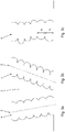
- Such a modified area with defects 3 is in Figure 1b represented as a linear chain of bubbles.
- the opening has a plurality of circumferential, concentric structures on the lateral surface, as shown in the illustrations Figures 2a and 2b such as Figure 3a to 3c can be seen.
- the recess 4 is formed as a result of successive etching of a plurality of defects 3 lined up one behind the other, in that the previously produced defects 3, which are enlarged by the etching effect to form a cavity in the workpiece 1, are successively connected by the etching process.
- the etching liquid quickly moves from defect 3 to defect 3. Because the influence of gravity is not decisive here, the etching progresses both from above and from below and starts on both outer sides at the same time. Due to the relatively longer exposure time of the caustic medium in the area of the outside, it comes about
- the etching process follows a line 5 on which the defects 3 are arranged.
- the line 5 can be a straight line or follow almost any contour that is precisely maintained by the etching process. This makes it possible for the first time to produce almost any cutting contour.
- the contour of the recess 4 or opening produced in this way is characterized by a sequence of cross-sectional enlargements and constrictions, the shape of which is pronounced of an earthworm, with the cross-sectional enlargements and constrictions neither having a matching cross-sectional area, as for example in figures 2b and 3c to recognize, still have a matching distance a1, a2, to adjacent cross-sectional extensions and constrictions must have, as in the Figure 3c is shown.
- a cross-sectional expansion or constriction can be in a cross-sectional plane to the main axis or, as in the Figure 3a shown, be arranged inclined thereto.
- Neighboring cross-sectional enlargements or constrictions can also have centers that lie on a common line 5 that is inclined relative to the surface of the workpiece 1, so that the cross-sectional enlargements or constrictions are offset from one another, with the cross-sectional enlargements or constrictions as in FIG Figure 3a shown inclined to the outer surface or as in the Figure 3b shown can be aligned parallel to the outer surface.
- the respective centroids of adjacent cross-sectional extensions have an offset, so that they are in particular not arranged on a common straight line.
Abstract
Die Erfindung betrifft ein Verfahren zum Einbringen mindestens einer Ausnehmung (4), insbesondere als eine Durchbrechung, in ein plattenförmiges Werkstück (1) mit einer Dicke kleiner als 3 Millimeter. Hierzu wird eine Laserstrahlung (2) auf die Oberfläche des Werkstückes (1) gerichtet. Die Einwirkungsdauer der Laserstrahlung (2) wird äußerst kurz gewählt, sodass lediglich eine Modifikation des Werkstückes (1) konzentrisch um eine Strahlachse des Laserstrahles eintritt. Ein derart modifizierter Bereich mit Fehlstellen (3) führt zu einer Kette von Bläschen. In einem nachfolgenden Verfahrensschritt kommt es aufgrund der Einwirkung eines ätzenden Mediums durch sukzessives Aufätzen zu einem anisotropen Materialabtrag in denjenigen, durch die Fehlstellen (3) gebildeten Bereichen des Werkstückes (1), die zuvor eine Modifikation durch die Laserstrahlung (2) erfahren haben. Entlang der zylindrischen Einwirkungszone entsteht dadurch eine Ausnehmung (4) als Durchbrechung in dem Werkstück (1).The invention relates to a method for making at least one recess (4), in particular as an opening, in a panel-shaped workpiece (1) with a thickness of less than 3 millimeters. For this purpose, a laser beam (2) is directed onto the surface of the workpiece (1). The exposure time of the laser radiation (2) is chosen to be extremely short, so that only a modification of the workpiece (1) occurs concentrically around a beam axis of the laser beam. Such a modified area with defects (3) leads to a chain of bubbles. In a subsequent process step, due to the action of an etching medium, successive etching leads to anisotropic material removal in those areas of the workpiece (1) formed by the defects (3) that have previously been modified by the laser radiation (2). This creates a recess (4) as an opening in the workpiece (1) along the cylindrical zone of action.
Description
Die Erfindung betrifft ein Verfahren zum Einbringen mindestens einer Ausnehmung oder Durchbrechung in ein plattenförmiges Werkstück mit einer Dicke kleiner als 3 Millimeter. Ein Mikrochip als Prozessorkern hat typischerweise auf seiner Unterseite auf relativ kleiner Fläche verteilt mehrere Hundert Kontaktpunkte in engem Abstand zueinander. Wegen dieses engen Abstandes können diese Kontaktpunkte nicht direkt auf eine Schaltungsplatte, das sogenannte Motherboard, aufgebracht werden. Es wird deshalb ein sogenannter Interposer aus isolierendem Material als Verbindungselement eingesetzt, mit welchem die Kontaktierungsbasis verbreitert werden kann. So eine Isolier- und Umverdrahtungsschicht besteht beispielsweise aus Glas, aus glasfaserverstärktem Epoxydharz oder Silizium und muss mit einer Vielzahl von Durchbrechungen versehen sein.The invention relates to a method for making at least one recess or opening in a plate-shaped workpiece with a thickness of less than 3 millimeters. A microchip as a processor core typically has several hundred closely spaced contact points distributed over a relatively small area on its underside. Because of this close spacing, these contact points cannot be applied directly to a circuit board, the so-called motherboard. A so-called interposer made of insulating material is therefore used as a connecting element, with which the contact base can be widened. Such an insulating and rewiring layer consists, for example, of glass, glass fiber reinforced epoxy resin or silicon and must be provided with a large number of openings.
Glas ist als Interposermaterial besonders vorteilhaft, da es kostengünstiger als Silizium ist und hinsichtlich seiner Temperaturausdehnung an die der aktiven Komponenten, beispielsweise Mikroprozessoren, angepasst werden kann. Als Herausforderung gestaltet sich die Verarbeitung des Glases zu gebrauchsfähigen Interposern. Insbesondere die wirtschaftliche Einbringung der Vielzahl an Durchbrechungen in das Glaswerkstück zur Durchkontaktierung ist im Stand der Technik noch nicht wirtschaftlich gelöst.Glass is particularly advantageous as an interposer material because it is cheaper than silicon and its temperature expansion can be adapted to that of the active components, for example microprocessors. The processing of the glass into usable interposers turns out to be a challenge. In particular, the economic introduction of the large number of openings in the glass workpiece for through-contacting has not yet been solved economically in the prior art.
So ist aus der
Ein Verfahren zur Bearbeitung von Glas durch die Erzeugung von Filamenten ist aus der
Der Erfindung liegt die Aufgabe zugrunde, dass nasschemisches oder Trockenätzen an Fehlstellen im Material anisotrop angreifen kann. Dadurch können in einem ersten Schritt erzeugte Fehlstellen sukzessive vergrößert werden und damit eine Ausnehmung oder Durchbrechung erzeugt werden. Dieses Verfahren erlaubt die Erzeugung einer Vielzahl von Ausnehmungen oder Durchbrechungen mit wesentlich verringertem Zeitaufwand. Die Aufgabe wird erfindungsgemäß mit einem Verfahren gemäß den Merkmalen des Anspruches 1 gelöst. Die weitere Ausgestaltung der Erfindung ist den Unteransprüchen zu entnehmen.The invention is based on the object that wet-chemical or dry etching can attack imperfections in the material anisotropically. As a result, defects produced in a first step can be successively enlarged and a recess or opening can thus be produced. This method allows the production of a large number of recesses or openings with a significantly reduced expenditure of time. The object is achieved according to the invention with a method according to the features of
Erfindungsgemäß ist also ein Verfahren vorgesehen, bei dem beispielsweise ein Laserstrahl derart kurzzeitig auf das Glaswerkstück gerichtet wird, dass lediglich eine Kette von Modifikationen im Material des Werkstückes, bevorzugt entlang einer Strahlachse des Laserstrahles erfolgt, ohne dass es zu einer Zerstörung des Werkstückes kommt, und bei dem im nächsten Schritt ein anisotroper Materialabtrag nur in denjenigen Bereichen des Werkstückes durchgeführt wird, die zuvor eine Fehlstelle mittels des Laserstrahles erfahren haben, und so eine Ausnehmung oder Durchbrechung in das Glaswerkstück eingebracht wird. Typischerweise wird durch die Laserstrahlung eine lineare Kette von Bläschen im Werkstück erzeugt. Die einzelnen Bläschen werden durch den Angriff des Ätzmediums vergrößert.According to the invention, a method is therefore provided in which, for example, a laser beam is directed onto the glass workpiece for such a short time that only a chain of modifications in the material of the workpiece occurs, preferably along a beam axis of the laser beam, without the workpiece being destroyed, and in which, in the next step, anisotropic material removal is carried out only in those areas of the workpiece that have previously experienced a defect by means of the laser beam, and a recess or opening is thus introduced into the glass workpiece. A linear chain of bubbles is typically generated in the workpiece by the laser radiation. The individual bubbles are enlarged by the attack of the etching medium.
Dabei soll im Sinne der vorliegenden Erfindung unter dem Begriff einer Durchbrechung eines Werkstückes eine durch die gesamte Dicke des Werkstückes verlaufende Öffnung wie beispielsweise eine Durchgangsbohrung verstanden werden, während eine nicht durch die gesamte Dicke des Werkstückes verlaufende Öffnung, wie beispielsweise ein Sackloch, als Ausnehmung bezeichnet wird.For the purposes of the present invention, the term perforation in a workpiece is to be understood as meaning an opening running through the entire thickness of the workpiece, such as a through hole, while an opening that does not run through the entire thickness of the workpiece, such as a blind hole, is referred to as a recess becomes.
Unter Fehlstellen sind im Folgenden lokal begrenzte Bläschen und/oder chemische Modifikation zu verstehen.In the following, defects are to be understood as meaning locally limited bubbles and/or chemical modification.
Die Ausnehmung oder Durchbrechung wird dabei infolge eines sukzessiven Aufätzens von einer Mehrzahl von aneinander gereihten Fehlstellen gebildet, indem durch den Ätzvorgang sukzessive die zuvor erzeugten Fehlstellen, die durch die Ätzwirkung zu einem Hohlraum in dem Werkstück erweitert werden, verbunden werden. Hierdurch gelangt die Ätzflüssigkeit schnell von Fehlstelle zu Fehlstelle. Dabei ist der Einfluss der Schwerkraft nicht entscheidend. Vielmehr gelingt der Ätzfortschritt in vergleichbarer Weise von oben nach unten wie umgekehrt, sodass insbesondere der Ätzvorgang an beiden Außenseiten zugleich beginnen kann.The recess or opening is formed as a result of successive etching of a plurality of defects in a row, in that the previously created defects, which are enlarged by the etching effect to form a cavity in the workpiece, are successively connected by the etching process. As a result, the etching liquid quickly moves from defect to defect. The influence of gravity is not decisive here. Rather, the etching progresses in a comparable manner from top to bottom and vice versa, so that in particular the etching process can begin on both outer sides at the same time.
Durch die Fehlstellen, die als Modifikationen innerhalb des Werkstückes erzeugt werden, folgt der Ätzvorgang der Linie, auf der die Fehlstellen angeordnet sind. Die Linie kann eine Gerade sein oder einer nahezu beliebigen Kontur folgen, die durch den Ätzvorgang präzise eingehalten wird. Somit ist es erstmals auch möglich, eine nahezu beliebige Schnittkontur zu erzeugen.Due to the defects that are created as modifications within the workpiece, the etching process follows the line on which the defects are arranged. The line can be a straight line or follow almost any contour that is precisely maintained by the etching process. This makes it possible for the first time to produce almost any cutting contour.
Obwohl es durch die längere Einwirkungsdauer im Bereich der den Außenseiten zugewandten Fehlstellen im Vergleich zu weiter innen in dem Werkstück liegenden Fehlstellen zu einer größeren Erweiterung kommt, ist dennoch eine insgesamt geringe kegelförmige Aufweitung zu beobachten. Die so erzeugte Kontur der Ausnehmung oder Durchbrechung ist nach dem Abschluss des Ätzvorganges durch eine Abfolge von Querschnittserweiterungen und Einschnürungen gekennzeichnet, wobei die Querschnittserweiterungen und Einschnürungen weder eine übereinstimmende Querschnittsfläche noch einen übereinstimmenden Abstand zu benachbarten Querschnittserweiterungen und Einschnürungen aufweisen müssen.Although the longer exposure time in the area of the imperfections facing the outside leads to a greater widening compared to imperfections located further inside in the workpiece, a slight conical widening overall can be observed. After the end of the etching process, the contour of the recess or opening produced in this way is characterized by a sequence of cross-sectional enlargements and constrictions, with the cross-sectional enlargements and constrictions neither having to have a matching cross-sectional area nor a matching distance from neighboring cross-sectional enlargements and constrictions.
Da eine so beschriebene Struktur der äußeren Gestalt eines Regenwurmes (lat. lumbricus terrestris) entspricht, würde der Fachmann diese als Regenwurmstruktur beschreiben.Since a structure described in this way corresponds to the external shape of an earthworm (lat. lumbricus terrestris), the person skilled in the art would describe it as an earthworm structure.
Unter den Begriff der Regenwurmstruktur fallen daher regelmäßige und unregelmäßige Querschnittserweiterungen und Einschnürungen, deren Übergang stetig oder unstetig sein kann. Eine Querschnittserweiterung oder Einschnürung kann dabei in einer Querschnittsebene zur Hauptachse oder geneigt hierzu verlaufen. Benachbarte Querschnittserweiterungen oder Einschnürungen können weiterhin auch Mittelpunkte aufweisen, die nicht auf derselben Geraden liegen, sodass die Querschnittserweiterungen oder Einschnürungen versetzt zueinander angeordnet sind. Auch die Höhe benachbarter Querschnittserweiterungen kann übereinstimmend sein oder voneinander abweichen. Ferner kann selbstverständlich auch die Hauptachse der Ausnehmung oder Durchbrechung abweichend von einer Flächennormalen zu der Oberfläche des Werkstückes geneigt verlaufen, während die Querschnittserweiterungen und Einschnürungen in einer zu der Oberfläche des Werkstückes parallelen Ebene ausgerichtet sind.The term earthworm structure therefore includes regular and irregular cross-sectional expansions and constrictions, the transition of which can be continuous or discontinuous. A cross-sectional enlargement or constriction can run in a cross-sectional plane to the main axis or inclined to it. Neighboring cross-sectional enlargements or constrictions can furthermore also have center points that do not lie on the same straight line, so that the cross-sectional enlargements or constrictions are offset from one another. The height of adjacent cross-sectional enlargements can also be the same or differ from one another. Furthermore, of course, the main axis of the recess or opening can also be inclined, deviating from a surface normal to the surface of the workpiece, while the cross-sectional enlargements and constrictions are aligned in a plane parallel to the surface of the workpiece.
Die Regenwurmstruktur ist dabei vergleichbar mit einem anderen, aus dem Stand der Technik bekannten Verfahren, welches als reaktives lonentiefenätzen (deep reactive ion etching, DRIE) bezeichnet wird. Dabei handelt es sich um einen anisotropen Trockenätzprozess, der ebenfalls für die Herstellung von Mikrostrukturen in Silicium beispielsweise für die Herstellung von Silizium-Durchkontaktierungen eingesetzt wird. Bei der Durchführung des erfindungsgemäßen Verfahrens müssen daher nachfolgende Prozesse nicht oder nur geringfügig angepasst werden.The earthworm structure is comparable to another method known from the prior art, which is referred to as deep reactive ion etching (DRIE). This is an anisotropic dry etching process that is also used for the production of microstructures in silicon, for example for the production of silicon vias. Therefore, when the method according to the invention is carried out, subsequent processes do not have to be adapted, or only slightly so.
Die Ausnehmung oder Durchbrechung wird dabei infolge eines sukzessiven Aufätzens von einer Mehrzahl von aneinander gereihten Fehlstellen gebildet, indem durch den Ätzvorgang sukzessive die zuvor erzeugten Fehlstellen, die durch die Ätzwirkung zu einem Hohlraum in dem Werkstück erweitert werden, verbunden werden. Hierdurch gelangt die Ätzflüssigkeit schnell von Fehlstelle zu Fehlstelle. Dabei ist der Einfluss der Schwerkraft nicht entscheidend. Vielmehr gelingt der Ätzfortschritt in vergleichbarer Weise von oben nach unten wie umgekehrt, sodass insbesondere der Ätzvorgang an beiden Außenseiten zugleich beginnen kann.The recess or opening is formed as a result of successive etching of a plurality of defects in a row, in that the previously created defects, which are enlarged by the etching effect to form a cavity in the workpiece, are successively connected by the etching process. As a result, the etching liquid quickly moves from defect to defect. The influence of gravity is not decisive here. Rather, the etching progresses in a comparable manner from top to bottom and vice versa, so that in particular the etching process can begin on both outer sides at the same time.
Durch die Fehlstellen, die als Modifikationen innerhalb des Werkstückes erzeugt werden, folgt der Ätzvorgang der Linie, auf der die Fehlstellen angeordnet sind. Die Linie kann eine Gerade sein oder einer nahezu beliebigen Kontur folgen, die durch den Ätzvorgang präzise eingehalten wird. Somit ist es erstmals auch möglich, eine nahezu beliebige Schnittkontur zu erzeugen.Due to the defects that are created as modifications within the workpiece, the etching process follows the line on which the defects are arranged. The line can be a straight line or follow almost any contour that is precisely maintained by the etching process. This makes it possible for the first time to produce almost any cutting contour.
Obwohl es durch die längere Einwirkungsdauer im Bereich der den Außenseiten zugewandten Fehlstellen im Vergleich zu weiter innen in dem Werkstück liegenden Fehlstellen zu einer größeren Erweiterung kommt, ist dennoch eine insgesamt geringe kegelförmige Aufweitung zu beobachten.Although it is due to the longer exposure time in the area of the defects facing the outside compared to those located further inside in the workpiece defects leads to a larger expansion, an overall slight conical expansion can nevertheless be observed.
Die so erzeugte Kontur der Ausnehmung oder Durchbrechung ist nach dem Abschluss des Ätzvorganges durch eine Abfolge von Querschnittserweiterungen und Einschnürungen gekennzeichnet, wobei die Querschnittserweiterungen und Einschnürungen weder eine übereinstimmende Querschnittsfläche noch einen übereinstimmenden Abstand zu benachbarten Querschnittserweiterungen und Einschnürungen aufweisen müssen. Die Differenz der Durchmesser von Querschnittserweiterung und Einschnürungen kann je nach Anzahl und Dichte der aufzuätzenden Fehlstellen weniger als 1 µm oder weniger als 100 nm betragen, sodass die Ausnehmung oder Durchbrechung sogar als makroskopisch glatt erscheinen kann.After the end of the etching process, the contour of the recess or opening produced in this way is characterized by a sequence of cross-sectional enlargements and constrictions, with the cross-sectional enlargements and constrictions neither having to have a matching cross-sectional area nor a matching distance from neighboring cross-sectional enlargements and constrictions. Depending on the number and density of the defects to be etched, the difference in the diameter of the cross-sectional expansion and constrictions can be less than 1 μm or less than 100 nm, so that the recess or opening can even appear macroscopically smooth.
Die Modifikationen im Glas können durch einen Laserstrahl hervorgerufen werden, welcher mithilfe eines diffraktiv-optischen Elementes so geformt wird, dass er eine lineare Kette von Modifikationen erzeugt. Die Modifikationen können durch eine Folge von Pulsen oder durch einen Einzelpuls erzeugt werden.The modifications in the glass can be caused by a laser beam, which is shaped using a diffractive optical element in such a way that it creates a linear chain of modifications. The modifications can be generated by a sequence of pulses or by a single pulse.
Aufgrund der Ausprägung des Verfahrens weisen erzeugte Ausnehmungen oder Durchbrechungen eine charakteristische Form auf. Da das grundsätzlich isotrop wirkende Ätzverfahren besonders stark an den modifizierten Bereichen im Werkstück angreift und der modifizierte Bereich typischerweise in Form einer linearen Kette von Modifikationen vorliegt, entstehen an den Mantelflächen der Ausnehmung oder Durchbrechung eine Mehrzahl von umlaufenden, konzentrischen Strukturen.Due to the nature of the method, the recesses or openings produced have a characteristic shape. Since the basically isotropic etching process acts particularly strongly on the modified areas in the workpiece and the modified area is typically present in the form of a linear chain of modifications, a plurality of peripheral, concentric structures are formed on the lateral surfaces of the recess or opening.
Aufgrund der Struktur der Durchbrechungen ist das Verfahren besonders gut für die Herstellung von Interposern geeignet, da die konzentrisch umlaufenden Mikrostrukturen, die in Folge des sukzessiven Aufätzens der Fehlstellen entstehen, für eine besonders gute Haftfestigkeit der späteren Metallschicht im Loch sorgen.Due to the structure of the openings, the process is particularly well suited for the production of interposers, since the concentric circumferential microstructures, which arise as a result of the successive etching of the defects, ensure particularly good adhesion of the later metal layer in the hole.
Besonders praxisrelevant ist der Einsatz derartiger Werkstücke als sogenannte Interposer zur elektrischen Verbindung der Anschlüsse mehrerer homogener oder heterogener Mikrochips. Ein Mikrochip als Prozessorkern hat typischerweise auf seiner Unterseite auf relativ kleiner Fläche verteilt mehrere Hundert Kontaktpunkte in engem Abstand zueinander. Wegen dieses engen Abstandes können diese Kontaktpunkte nicht direkt auf eine Schaltungsplatte, das sogenannte Motherboard, aufgebracht werden. Es wird deshalb ein Interposer als Verbindungselement eingesetzt, mit welchem die Kontaktierungsbasis verbreitert werden kann.The use of such workpieces as so-called interposers for the electrical connection of the connections of several homogeneous or heterogeneous microchips is particularly relevant in practice. A microchip as a processor core typically has several hundred closely spaced contact points distributed over a relatively small area on its underside. Because of this close spacing, these contact points cannot be applied directly to a circuit board, the so-called motherboard. An interposer is therefore used as a connecting element, with which the contact base can be widened.
Ein derartiger Interposer besteht vorzugsweise aus Glas oder Silizium und enthält beispielsweise Kontaktflächen, Umverdrahtungen, Durchkontaktierungen sowie aktive und nicht aktive Komponenten.Such an interposer is preferably made of glass or silicon and contains, for example, contact surfaces, rewiring, vias and active and inactive components.
Es ist bereits erkannt worden, dass erfindungsgemäß der Abstand der derart einzubringenden Ausnehmungen weiter reduziert werden kann, weil es durch die Laserstrahlung nicht zu einer Zerstörung des Werkstückes, sondern lediglich zu einer Modifikation oder Umwandlung kommt, wobei zugleich auch die Laserleistung vermindert werden kann. Besonders bevorzugt wird der Laser mit einer Wellenlänge betrieben, für die das Glaswerkstück transparent ist, sodass eine Durchdringung des Glaswerkstückes sichergestellt ist. Insbesondere wird dadurch eine im Wesentlichen zylindrische Modifikationszone koaxial zu der Laserstrahlachse herum sichergestellt, die zu einem konstanten Durchmesser der Durchbrechung oder der Ausnehmung führt.It has already been recognized that, according to the invention, the distance between the recesses to be made in this way can be further reduced because the laser radiation does not destroy the workpiece, but merely modifies it or transforms it, with the laser power also being able to be reduced at the same time. The laser is particularly preferably operated with a wavelength for which the glass workpiece is transparent, so that penetration of the glass workpiece is ensured. In particular, this ensures a substantially cylindrical modification zone coaxial to the laser beam axis, which results in a constant diameter of the opening or recess.
Besonders vorteilhaft für die Siliziumbearbeitung ist eine Wellenlänge größer als 1,1 µm.A wavelength greater than 1.1 µm is particularly advantageous for silicon processing.
Besonders vorteilhaft bei der Erzeugung von Ausnehmungen oder Durchbrechungen in dem Werkstück, insbesondere aus Silizium, ist eine Ausrichtung der Ausbreitungsrichtung des Laserstrahls in einem Winkel der Strahlachse von ungefähr 0°, 45° oder 90° zur Kristallsymmetrie.Aligning the propagation direction of the laser beam at an angle of the beam axis of approximately 0°, 45° or 90° to the crystal symmetry is particularly advantageous when producing recesses or openings in the workpiece, in particular made of silicon.
Die Pulsdauer kann gegenüber dem aus dem Stand der Technik bekannten Verfahren wesentlich reduziert werden. Bei einer besonders vorteilhaften Ausgestaltung des erfindungsgemäßen Verfahrens kann der Laser mit einer Pulsdauer von weniger als 100 Nanosekunden bis unter 1 Pikosekunden betrieben werden.The pulse duration can be significantly reduced compared to the method known from the prior art. In a particularly advantageous embodiment of the method according to the invention, the laser can be operated with a pulse duration of less than 100 nanoseconds to less than 1 picosecond.
Bei geeigneter Wahl von Pulsenergie und Pulsdauer, vor allem bei der bevorzugten Verwendung von Pulsfolgen mit einer Wiederholrate im Megahertz-Bereich und Pulsdauern kleiner als 10 Pikosekunden, entstehen Filamente aufgrund von gegenläufigen Effekten, nämlich der Selbstfokussierung aufgrund des Kerr-Effektes und der Defokussierung durch Beugung aufgrund des kleinen Strahldurchmessers.With a suitable choice of pulse energy and pulse duration, especially with the preferred use of pulse sequences with a repetition rate in the megahertz range and pulse durations of less than 10 picoseconds, filaments arise due to opposing effects, namely self-focusing due to the Kerr effect and defocusing due to diffraction due to the small beam diameter.
Grundsätzlich ist das Verfahren nicht auf bestimmte Materialien des Werkstückes beschränkt. Erfolg versprechend ist, wenn ein dielektrisches Material wie Glas verwendet wird. Besonders Erfolg versprechend ist es, wenn Glas mit einem wesentlichen Materialanteil an Aluminosilikat, insbesondere ein Boro-Aluminosilikat, eingesetzt wird.Basically, the process is not limited to certain materials of the workpiece. It is promising if a dielectric material such as glass is used. It is particularly promising if glass with a significant proportion of material made of aluminosilicate, in particular a boroaluminosilicate, is used.
Vorzugsweise wird das Werkstück zumindest in seinen modifizierten Bereichen beispielsweise durch ein Ätzverfahren, wie beispielsweise durch Flüssigätzen, Trockenätzen oder Dampfphasenätzen, oder durch Verdampfen mittels Hochspannung oder Hochfrequenz einem anisotropen Materialabtrag unterzogen, um so Ausnehmungen oder Durchbrechungen in das Werkstück einzubringen . Durch den anisotropen Materialabtrag ist für den eigentlichen Materialabtrag kein sequentielles, sondern ein flächig einwirkendes Abtragsverfahren nutzbar, welches lediglich geringe Anforderungen an den Prozess stellt. Vielmehr lässt sich über die Einwirkungsdauer der Materialabtrag quantitativ und qualitativ für alle in der beschriebenen Weise vorbehandelten und dementsprechend modifizierten Bereiche zugleich durchführen, sodass der Zeitaufwand für die Erzeugung der Vielzahl der Ausnehmungen oder Durchbrechungen in der Summe wesentlich reduziert ist.The workpiece is preferably subjected to anisotropic material removal, at least in its modified areas, for example by an etching process such as liquid etching, dry etching or vapor phase etching, or by evaporation using high voltage or high frequency, in order to introduce recesses or openings in the workpiece. Due to the anisotropic material removal, no sequential removal process can be used for the actual material removal, but rather a planar removal method, which only places low demands on the process. Rather, the material can be removed quantitatively and qualitatively for all the areas that have been pretreated in the manner described and modified accordingly over the duration of the exposure, so that the total time required for producing the large number of recesses or openings is significantly reduced.
Durch ein Gleichgewicht beider Effekte kann der Laserstrahl durch das für die Wellenlänge transparente Werkstück propagieren, wobei sein Durchmesser zumindest im Wesentlichen konstant bleibt.By balancing both effects, the laser beam can propagate through the workpiece, which is transparent for the wavelength, with its diameter remaining at least essentially constant.
Dabei können bei hohen Spitzenintensitäten im Laserstrahl in vorteilhafter Weise auch weitere Effekte, wie Plasmabildung, zur stärkeren Defokussierung genutzt werden.In the case of high peak intensities in the laser beam, other effects such as plasma formation can also be used in an advantageous manner for greater defocusing.
In der Praxis verläuft das Wechselspiel zwischen Defokussierung und Selbstfokussierung periodisch, sodass eine Kette von modifizierten Materialbereichen entsteht. Je nach Ausprägung der Effekte kann auch ein zusammenhängender Kanal, ein sogenannter Plasmakanal entstehen.In practice, the interplay between defocusing and self-focusing runs periodically, resulting in a chain of modified material areas. Depending on the extent of the effects, a coherent channel, a so-called plasma channel, can also develop.
Grundsätzlich kann die Ausbildung des Filamentes auf einen Teilabschnitt der maximalen Materialstärke des Materials beschränkt bleiben. Die Ausbildung des Filamentes endet, wenn der Strahl das Kerr-Medium verlässt und divergiert oder wenn die Intensität des Strahles so weit abgenommen hat, dass die defokussierende Beugung die Selbstfokussierung überwiegt.In principle, the formation of the filament can remain limited to a section of the maximum material thickness of the material. The formation of the filament ends when the beam leaves the Kerr medium and diverges, or when the intensity of the beam has decreased to the point where defocusing diffraction outweighs selffocusing.
Als Interposer wird in der Praxis beispielsweise eine mit Glasfaser verstärkte Epoxydharzplatte eingesetzt, die mit einer Anzahl von Löchern versehen ist. Auf der Oberfläche der Glasfasermatte laufen Leiterbahnen, die in die jeweiligen Löcher hineinführen, um diese zu verfüllen, und auf der anderen Seite der Glasfasermatte bis zu den Anschlusskontakten des Prozessorkernes führen. Bei Auftreten von Erwärmung kommt es allerdings zu unterschiedlichen Ausdehnungen zwischen dem Kernprozessor und der Glasfasermatte und damit zu mechanischen Spannungen zwischen diesen beiden Komponenten.In practice, for example, an epoxy resin plate reinforced with glass fiber and provided with a number of holes is used as an interposer. Conductor tracks run on the surface of the glass fiber mat, which lead into the respective holes in order to fill them up, and on the other side of the glass fiber mat to the connection contacts of the processor core. When heating occurs, however, there are different expansions between the core processor and the Glass fiber mat and thus to mechanical stresses between these two components.
Die Filamente könnten durch eine Laserbearbeitung eingebracht werden, bei der eine Positionierung des Bearbeitungskopfes und die Bestrahlung abwechselnd durchgeführt werden. Vorzugsweise wird hingegen, während die Strahlung auf das Werkstück gelenkt wird, eine stetige Relativbewegung zwischen dem Bearbeitungskopf und dem Werkstück vorgenommen, sodass also der Laserstrahl kontinuierlich in einer "fliegenden" Bewegung über das Werkstück geführt wird, sodass also eine ununterbrochene Änderung der Relativposition eine extrem schnelle Bearbeitungsdauer ergibt.The filaments could be introduced by laser processing, in which the positioning of the processing head and the irradiation are carried out alternately. Preferably, on the other hand, while the radiation is directed onto the workpiece, a constant relative movement is carried out between the processing head and the workpiece, so that the laser beam is continuously guided in a "flying" movement over the workpiece, so that an uninterrupted change in the relative position is extremely quick processing time.
Dabei kann die relative Position des Materials in Bezug auf den Bearbeitungskopf mit konstanter Geschwindigkeit verändert werden, sodass bei einer konstanten Pulsfrequenz der Abstand der zu erzeugenden Modifikationen einem vorbestimmten Rastermaß folgt.The relative position of the material in relation to the processing head can be changed at a constant speed, so that the distance between the modifications to be produced follows a predetermined grid dimension at a constant pulse frequency.
Besonders bevorzugt wird die Strahlungsquelle mit einer Wellenlänge betrieben, für die das Werkstück transparent ist, sodass eine Durchdringung des Werkstückes sichergestellt ist. Insbesondere wird dadurch eine im Wesentlichen zylindrische Modifikationszone koaxial zu der Strahlachse herum sichergestellt, die zu einem konstanten Durchmesser der Durchbrechung oder der Ausnehmung führt.The radiation source is particularly preferably operated with a wavelength for which the workpiece is transparent, so that penetration of the workpiece is ensured. In particular, this ensures a substantially cylindrical modification zone coaxial to the beam axis, which results in a constant diameter of the aperture or recess.
Darüber hinaus kann es auch von Vorteil sein, wenn durch die Strahlungsquelle zusätzlich auch ein Oberflächenbereich abgetragen wird, um die Einwirkungszone des anisotropen Abtrages derart auszugestalten, dass ein kegelförmiger Einlassbereich der Filamente entsteht. Auf diese Weise kann die spätere Durchkontaktierung vereinfacht werden. Zudem wird in diesem Bereich beispielsweise die Einwirkung eines Ätzmittels konzentriert.In addition, it can also be advantageous if a surface area is also removed by the radiation source in order to design the zone of action of the anisotropic removal in such a way that a conical inlet area of the filaments is created. In this way, later through-plating can be simplified. In addition, the effect of an etchant, for example, is concentrated in this area.
Bei einer Ausgestaltung des erfindungsgemäßen Verfahrens kann die Strahlungsquelle mit einer Pulsdauer von weniger als 50 ps, vorzugsweise weniger als 10 ps betrieben werden.In one embodiment of the method according to the invention, the radiation source can be operated with a pulse duration of less than 50 ps, preferably less than 10 ps.
Bei einer anderen, ebenfalls besonders Erfolg versprechenden Ausgestaltung der Erfindung wird das Werkstück insbesondere nach der Modifikation mit einer flächigen, zumindest einzelnen, insbesondere eine Vielzahl von nachfolgend einzubringenden Durchbrechungen abdeckenden Metallschicht versehen. In einem folgenden Schritt werden die modifizierten Bereiche so abgetragen, dass eine von der Metallschicht einseitig verschlossene Ausnehmung erzeugt wird. Dabei wird die Metallschicht vorzugsweise nach der Modifikation, jedoch vor dem Materialabtrag aufgebracht, sodass nach dem Materialabtrag die beispielsweise als Leiterbahn aufgebrachte Metallschicht die Ausnehmung verschließt und dadurch zugleich eine optimale Basis für eine daran anzubringende Kontaktierung bildet. Die Durchkontaktierung erfolgt dabei im Bereich der Ausnehmung mit an sich bekannten Verfahren. Indem die Metallschicht als Leiterbahn aufgebracht wird, kann zudem in einfacher Weise ein gewünschtes Schaltbild erzeugt werden.In another embodiment of the invention that also promises particularly success, the workpiece is provided, in particular after the modification, with a flat metal layer covering at least individual openings, in particular a large number of openings to be made subsequently. In a subsequent step, the modified areas are removed in such a way that a recess closed on one side by the metal layer is produced. The metal layer is preferably applied after the modification, but before the material is removed, so that after the material is removed metal layer applied, for example as a conductor track, closes the recess and thereby at the same time forms an optimal basis for a contact to be attached thereto. The through-contacting takes place in the area of the recess using methods known per se. In addition, by applying the metal layer as a conductor track, a desired circuit diagram can be produced in a simple manner.
Bei einer anderen, ebenfalls besonders Erfolg versprechenden Ausgestaltung des Verfahrens wird das Werkstück vor einer Laserbehandlung mit einem Ätzresist auf zumindest einer Oberfläche flächig beschichtet. Durch Einwirkung des Laserstrahles als bevorzugte elektromagnetische Strahlungsquelle wird zugleich in einer punktförmigen Einwirkungszone das Ätzresist auf zumindest einer Oberfläche abgetragen und die Modifikation in dem Werkstück erzeugt. Auf diese Weise werden die nicht modifizierten Bereiche vor einer unerwünschten Einwirkung im nachfolgenden Ätzprozess geschützt und die Oberfläche des Materials daher nicht beeinträchtigt. Dabei behindert das Ätzresist nicht die Modifikation des darunter liegenden Materials. Vielmehr ist das Ätzresist für die Laserstrahlung entweder durchlässig oder wird nahezu punktförmig durch die Laserstrahlung abgetragen, beispielsweise also verdampft. Weiterhin ist nicht ausgeschlossen, dass das Ätzresist solche Substanzen enthält, die für die Modifikation unterstützend wirken, beispielsweise also den Modifikationsvorgang beschleunigen.In another embodiment of the method that is also particularly promising, the workpiece is coated with an etching resist over at least one surface before a laser treatment. Through the action of the laser beam as the preferred electromagnetic radiation source, the etching resist is simultaneously removed from at least one surface in a punctiform zone of action and the modification is produced in the workpiece. In this way, the unmodified areas are protected from undesirable effects in the subsequent etching process and the surface of the material is therefore not affected. The etch resist does not hinder the modification of the underlying material. Rather, the etching resist is either permeable to the laser radiation or is removed almost in a point-like manner by the laser radiation, ie vaporized, for example. Furthermore, it cannot be ruled out that the etching resist contains substances that have a supporting effect on the modification, ie for example accelerate the modification process.
Selbstverständlich kann vor dem Auftrag des Ätzresists auf eine der Außenflächen des Materials die vorstehend beschriebene Metallschicht aufgebracht werden, um diese nach dem Entfernen des Ätzresists als Basis für die gewünschte Durchkontaktierung zu verwenden.Of course, prior to the application of the etch resist to one of the outer surfaces of the material, the metal layer described above can be applied in order to use this as a base for the desired via hole after the etch resist has been removed.
Das Ätzresist könnte nach dem Abschluss der Behandlung auf der Oberfläche des Materials verbleiben. Vorzugsweise wird jedoch das Ätzresist in an sich bekannter Weise nach dem anisotropen Materialabtrag von der Oberfläche des Materials entfernt.The etch resist could remain on the surface of the material after the treatment is completed. However, the etching resist is preferably removed from the surface of the material in a manner known per se after the anisotropic removal of material.
Grundsätzlich ist das Verfahren nicht auf bestimmte Materialzusammensetzungen des Materials beschränkt. Besonders Erfolg versprechend ist es allerdings, wenn das Werkstück als einen wesentlichen Materialanteil ein Aluminosilikat, insbesondere ein Boro-Aluminosilikat aufweist.In principle, the method is not limited to specific material compositions of the material. However, it is particularly promising if the workpiece has an aluminosilicate, in particular a boroaluminosilicate, as a significant proportion of the material.
Bei einer anderen, ebenfalls besonders praxisgerechten Ausgestaltung der Erfindung wird der Abstand benachbart in dem Werkstück erzeugter Filamente entlang einer Trennlinie derart realisiert, dass die modifizierten Bereiche unmittelbar aneinandergrenzen oder einen sehr geringen Abstand zueinander aufweisen, um auf diese Weise definierte Materialbereiche abzutrennen.In another, likewise particularly practical embodiment of the invention, the distance between filaments produced adjacently in the workpiece is realized along a dividing line in such a way that the modified areas directly adjoin one another or form a have a very small distance from each other in order to separate defined material areas in this way.
Die Trennung erfolgt nach dem Einbringen der Filamente entlang der Trennlinie infolge von inneren Spannungen des Materials oder aufgrund einer äußeren Krafteinwirkung. Alternativ oder ergänzend können die inneren Spannungen auch durch thermische Spannungen, insbesondere durch eine starke Temperaturdifferenz hervorgerufen werden.The separation occurs after the insertion of the filaments along the separation line as a result of internal stresses in the material or as a result of an external force. Alternatively or additionally, the internal stresses can also be caused by thermal stresses, in particular by a large temperature difference.
Die Erfindung lässt verschiedene Ausführungsformen zu. Zur weiteren Verdeutlichung ihres Grundprinzips ist eine davon in der Zeichnung dargestellt und wird nachfolgend beschrieben. Diese zeigt jeweils in einer Prinzipdarstellung in
- Fig. 1
- einen Verfahrensablauf beim Einbringen von Ausnehmungen in ein Werkstück;
- Fig. 2
- mögliche Ausprägungen verschiedener Ausnehmungen;
- Fig. 3
- weitere mögliche Ausprägungen verschiedener Ausnehmungen.
- 1
- a process sequence when making recesses in a workpiece;
- 2
- possible characteristics of different recesses;
- 3
- other possible forms of different recesses.
Die Durchbrechung weist eine Mehrzahl umlaufender, konzentrischer Strukturen auf der Mantelfläche auf, wie in den Darstellungen der
Die Ausnehmung 4 wird dabei infolge eines sukzessiven Aufätzens von einer Mehrzahl von aneinander gereihten Fehlstellen 3 gebildet, indem durch den Ätzvorgang sukzessive die zuvor erzeugten Fehlstellen 3, die durch die Ätzwirkung zu einem Hohlraum in dem Werkstück 1 erweitert werden, verbunden werden. Hierdurch gelangt die Ätzflüssigkeit schnell von Fehlstelle 3 zu Fehlstelle 3. Weil dabei der Einfluss der Schwerkraft nicht entscheidend ist erfolgt der Ätzfortschritt sowohl von oben als auch von unten und beginnt zugleich an beiden Außenseiten. Durch die im Verhältnis längere Einwirkungsdauer des ätzenden Mediums im Bereich der Außenseiten kommt esThe
zu einer konischen Erweiterung der Fehlstellen 3 im Bereich der äußeren Oberflächen wie in der
Durch die Fehlstellen 3, die als Modifikationen innerhalb des Werkstückes 1 erzeugt werden, folgt der Ätzvorgang einer Linie 5, auf der die Fehlstellen 3 angeordnet sind. Die Linie 5 kann eine Gerade sein oder einer nahezu beliebigen Kontur folgen, die durch den Ätzvorgang präzise eingehalten wird. Somit ist es erstmals auch möglich, eine nahezu beliebige Schnittkontur zu erzeugen.Due to the
Obwohl es durch die längere Einwirkungsdauer im Bereich der den Außenseiten zugewandten Fehlstellen 3 im Vergleich zu weiter innen in dem Werkstück liegenden Fehlstellen 3 zu einer größeren Erweiterung kommt, ist dennoch eine insgesamt geringe kegelförmige Aufweitung zu beobachten.Although the longer exposure time in the area of the
Die so erzeugte Kontur der Ausnehmung 4 oder Durchbrechung ist nach dem Abschluss des Ätzvorganges durch eine Abfolge von Querschnittserweiterungen und Einschnürungen gekennzeichnet, deren Gestalt an einen Regenwurm erinnert, wobei die Querschnittserweiterungen und Einschnürungen weder eine übereinstimmende Querschnittsfläche, wie beispielsweise in den
Benachbarte Querschnittserweiterungen oder Einschnürungen können weiterhin auch Mittelpunkte aufweisen, die auf einer gemeinsamen, gegenüber der Oberfläche des Werkstückes 1 geneigten Linie 5 liegen, sodass die Querschnittserweiterungen oder Einschnürungen versetzt zueinander angeordnet sind, wobei die Querschnittserweiterungen oder Einschnürungen wie in der
Wie in der
Claims (16)
Applications Claiming Priority (4)
| Application Number | Priority Date | Filing Date | Title |
|---|---|---|---|
| DE102014113339.0A DE102014113339A1 (en) | 2014-09-16 | 2014-09-16 | Method for producing recesses in a material |
| DE102014116291 | 2014-11-07 | ||
| EP15762474.3A EP3195706B1 (en) | 2014-09-16 | 2015-08-07 | Method for introducing at least one cutout or aperture into a sheetlike workpiece |
| PCT/DE2015/100333 WO2016041544A1 (en) | 2014-09-16 | 2015-08-07 | Method for introducing at least one cutout or aperture into a sheetlike workpiece |
Related Parent Applications (2)
| Application Number | Title | Priority Date | Filing Date |
|---|---|---|---|
| EP15762474.3A Division-Into EP3195706B1 (en) | 2014-09-16 | 2015-08-07 | Method for introducing at least one cutout or aperture into a sheetlike workpiece |
| EP15762474.3A Division EP3195706B1 (en) | 2014-09-16 | 2015-08-07 | Method for introducing at least one cutout or aperture into a sheetlike workpiece |
Publications (1)
| Publication Number | Publication Date |
|---|---|
| EP4061101A1 true EP4061101A1 (en) | 2022-09-21 |
Family
ID=54072638
Family Applications (2)
| Application Number | Title | Priority Date | Filing Date |
|---|---|---|---|
| EP15762474.3A Active EP3195706B1 (en) | 2014-09-16 | 2015-08-07 | Method for introducing at least one cutout or aperture into a sheetlike workpiece |
| EP22167179.5A Pending EP4061101A1 (en) | 2014-09-16 | 2015-08-07 | Method for creating at least one recess or opening in a plate-shaped workpiece |
Family Applications Before (1)
| Application Number | Title | Priority Date | Filing Date |
|---|---|---|---|
| EP15762474.3A Active EP3195706B1 (en) | 2014-09-16 | 2015-08-07 | Method for introducing at least one cutout or aperture into a sheetlike workpiece |
Country Status (11)
| Country | Link |
|---|---|
| US (2) | US11610784B2 (en) |
| EP (2) | EP3195706B1 (en) |
| JP (2) | JP6782692B2 (en) |
| KR (4) | KR20210022773A (en) |
| CN (1) | CN107006128B (en) |
| ES (1) | ES2923764T3 (en) |
| LT (1) | LT3195706T (en) |
| MY (1) | MY196621A (en) |
| SG (2) | SG10201902331XA (en) |
| TW (1) | TWI616939B (en) |
| WO (1) | WO2016041544A1 (en) |
Families Citing this family (14)
| Publication number | Priority date | Publication date | Assignee | Title |
|---|---|---|---|---|
| DE102018100299A1 (en) * | 2017-01-27 | 2018-08-02 | Schott Ag | Structured plate-shaped glass element and method for its production |
| EP3967442A1 (en) | 2017-03-06 | 2022-03-16 | LPKF Laser & Electronics AG | Method for producing a technical mask |
| US11478880B2 (en) | 2017-03-06 | 2022-10-25 | Lpkf Laser & Electronics Ag | Method for producing at least one recess in a material by means of electromagnetic radiation and subsequent etching process |
| DE102018110211A1 (en) * | 2018-04-27 | 2019-10-31 | Schott Ag | Method for producing fine structures in the volume of a substrate made of brittle-hard material |
| TWI678342B (en) * | 2018-11-09 | 2019-12-01 | 財團法人工業技術研究院 | Cutting method for forming chamfered corners |
| DE102020100848B4 (en) | 2019-01-29 | 2023-07-27 | Lpkf Laser & Electronics Aktiengesellschaft | Process for microstructuring a glass substrate using laser radiation |
| DE102019201347B3 (en) * | 2019-02-01 | 2020-06-18 | Lpkf Laser & Electronics Ag | Manufacture of metallic conductor tracks on glass |
| DE102019121827A1 (en) * | 2019-08-13 | 2021-02-18 | Trumpf Laser- Und Systemtechnik Gmbh | Laser etching with varying etching selectivity |
| CN113594014B (en) * | 2020-04-30 | 2024-04-12 | 中微半导体设备(上海)股份有限公司 | Component, plasma reaction device, and component processing method |
| DE102020114195A1 (en) | 2020-05-27 | 2021-12-02 | Lpkf Laser & Electronics Aktiengesellschaft | Method for making a recess in a substrate |
| CN111799169A (en) * | 2020-07-17 | 2020-10-20 | 绍兴同芯成集成电路有限公司 | Process for processing TGV by combining femtosecond laser with HF wet etching |
| DE102021204675B4 (en) | 2021-05-07 | 2023-05-17 | Lpkf Laser & Electronics Se | Device and method for cell cultivation |
| CN113510364B (en) * | 2021-07-28 | 2022-11-25 | 广东工业大学 | Forming method of three-dimensional cavity structure based on laser-assisted dissolution |
| EP4296244A1 (en) | 2022-06-21 | 2023-12-27 | LPKF Laser & Electronics SE | Substrate carrier made of glass for processing a substrate and a method for producing the same |
Citations (7)
| Publication number | Priority date | Publication date | Assignee | Title |
|---|---|---|---|---|
| WO2001015819A1 (en) * | 1999-08-30 | 2001-03-08 | Board Of Regents University Of Nebraska-Lincoln | Three-dimensional electrical interconnects |
| DE102010025966B4 (en) | 2010-07-02 | 2012-03-08 | Schott Ag | Interposer and method for making holes in an interposer |
| US20120125893A1 (en) * | 2010-07-26 | 2012-05-24 | Hamamatsu Photonics K.K. | Laser processing method |
| US20120125887A1 (en) * | 2010-07-26 | 2012-05-24 | Hamamatsu Photonics K.K. | Method for manufacturing light-absorbing substrate and method for manufacturing mold for making same |
| US20120142186A1 (en) * | 2010-07-26 | 2012-06-07 | Hamamatsu Photonics K.K. | Method for manufacturing interposer |
| US20130029093A1 (en) * | 2010-04-08 | 2013-01-31 | Fujikura Ltd. | Method of forming microstructure, laser irradiation device, and substrate |
| US20130126573A1 (en) | 2010-07-12 | 2013-05-23 | Filaser Inc. | Method of material processing by laser filamentation |
Family Cites Families (12)
| Publication number | Priority date | Publication date | Assignee | Title |
|---|---|---|---|---|
| JP4880820B2 (en) | 2001-01-19 | 2012-02-22 | 株式会社レーザーシステム | Laser assisted machining method |
| JP4418282B2 (en) | 2004-03-31 | 2010-02-17 | 株式会社レーザーシステム | Laser processing method |
| JP4222296B2 (en) | 2004-11-22 | 2009-02-12 | 住友電気工業株式会社 | Laser processing method and laser processing apparatus |
| US9138913B2 (en) | 2005-09-08 | 2015-09-22 | Imra America, Inc. | Transparent material processing with an ultrashort pulse laser |
| US8933367B2 (en) * | 2011-02-09 | 2015-01-13 | Sumitomo Electric Industries, Ltd. | Laser processing method |
| EP2925690B1 (en) | 2012-11-29 | 2021-08-11 | Corning Incorporated | Methods of fabricating glass articles by laser damage and etching |
| EP2754524B1 (en) | 2013-01-15 | 2015-11-25 | Corning Laser Technologies GmbH | Method of and apparatus for laser based processing of flat substrates being wafer or glass element using a laser beam line |
| JP6113529B2 (en) * | 2013-03-05 | 2017-04-12 | 株式会社ディスコ | Wafer processing method |
| DE102013223637B4 (en) | 2013-11-20 | 2018-02-01 | Trumpf Laser- Und Systemtechnik Gmbh | A method of treating a laser transparent substrate for subsequently separating the substrate |
| US10293436B2 (en) * | 2013-12-17 | 2019-05-21 | Corning Incorporated | Method for rapid laser drilling of holes in glass and products made therefrom |
| KR20190078595A (en) * | 2016-11-04 | 2019-07-04 | 코닝 인코포레이티드 | A micro-perforated panel system, an application, and a method of manufacturing a micro-perforated panel system |
| US11344973B2 (en) * | 2018-04-19 | 2022-05-31 | Corning Incorporated | Methods for forming holes in substrates |
-
2015
- 2015-08-07 SG SG10201902331XA patent/SG10201902331XA/en unknown
- 2015-08-07 EP EP15762474.3A patent/EP3195706B1/en active Active
- 2015-08-07 MY MYPI2017700845A patent/MY196621A/en unknown
- 2015-08-07 KR KR1020217005121A patent/KR20210022773A/en not_active IP Right Cessation
- 2015-08-07 KR KR1020177007041A patent/KR20170044143A/en active Application Filing
- 2015-08-07 SG SG11201702091WA patent/SG11201702091WA/en unknown
- 2015-08-07 ES ES15762474T patent/ES2923764T3/en active Active
- 2015-08-07 JP JP2017512917A patent/JP6782692B2/en active Active
- 2015-08-07 KR KR1020197015976A patent/KR20190065480A/en not_active IP Right Cessation
- 2015-08-07 US US15/511,272 patent/US11610784B2/en active Active
- 2015-08-07 EP EP22167179.5A patent/EP4061101A1/en active Pending
- 2015-08-07 KR KR1020237018486A patent/KR20230084606A/en not_active Application Discontinuation
- 2015-08-07 CN CN201580049903.1A patent/CN107006128B/en active Active
- 2015-08-07 WO PCT/DE2015/100333 patent/WO2016041544A1/en active Application Filing
- 2015-08-07 LT LTEPPCT/DE2015/100333T patent/LT3195706T/en unknown
- 2015-09-09 TW TW104129751A patent/TWI616939B/en active
-
2020
- 2020-07-09 JP JP2020118488A patent/JP7049404B2/en active Active
-
2022
- 2022-04-01 US US17/711,136 patent/US20220223434A1/en active Pending
Patent Citations (7)
| Publication number | Priority date | Publication date | Assignee | Title |
|---|---|---|---|---|
| WO2001015819A1 (en) * | 1999-08-30 | 2001-03-08 | Board Of Regents University Of Nebraska-Lincoln | Three-dimensional electrical interconnects |
| US20130029093A1 (en) * | 2010-04-08 | 2013-01-31 | Fujikura Ltd. | Method of forming microstructure, laser irradiation device, and substrate |
| DE102010025966B4 (en) | 2010-07-02 | 2012-03-08 | Schott Ag | Interposer and method for making holes in an interposer |
| US20130126573A1 (en) | 2010-07-12 | 2013-05-23 | Filaser Inc. | Method of material processing by laser filamentation |
| US20120125893A1 (en) * | 2010-07-26 | 2012-05-24 | Hamamatsu Photonics K.K. | Laser processing method |
| US20120125887A1 (en) * | 2010-07-26 | 2012-05-24 | Hamamatsu Photonics K.K. | Method for manufacturing light-absorbing substrate and method for manufacturing mold for making same |
| US20120142186A1 (en) * | 2010-07-26 | 2012-06-07 | Hamamatsu Photonics K.K. | Method for manufacturing interposer |
Also Published As
| Publication number | Publication date |
|---|---|
| CN107006128B (en) | 2020-05-19 |
| EP3195706A1 (en) | 2017-07-26 |
| KR20230084606A (en) | 2023-06-13 |
| CN107006128A (en) | 2017-08-01 |
| KR20210022773A (en) | 2021-03-03 |
| EP3195706B1 (en) | 2022-06-01 |
| US20170256422A1 (en) | 2017-09-07 |
| WO2016041544A1 (en) | 2016-03-24 |
| SG11201702091WA (en) | 2017-04-27 |
| US11610784B2 (en) | 2023-03-21 |
| SG10201902331XA (en) | 2019-04-29 |
| TWI616939B (en) | 2018-03-01 |
| US20220223434A1 (en) | 2022-07-14 |
| JP6782692B2 (en) | 2020-11-11 |
| ES2923764T3 (en) | 2022-09-30 |
| KR20190065480A (en) | 2019-06-11 |
| JP7049404B2 (en) | 2022-04-06 |
| MY196621A (en) | 2023-04-23 |
| TW201621986A (en) | 2016-06-16 |
| LT3195706T (en) | 2022-08-10 |
| JP2020185613A (en) | 2020-11-19 |
| JP2017534458A (en) | 2017-11-24 |
| KR20170044143A (en) | 2017-04-24 |
Similar Documents
| Publication | Publication Date | Title |
|---|---|---|
| EP3195706B1 (en) | Method for introducing at least one cutout or aperture into a sheetlike workpiece | |
| EP2964417B1 (en) | Method for providing through-openings in a substrate | |
| EP2964416B1 (en) | Method for separating a substrate | |
| EP3592500B1 (en) | Process for manufacturing a recess in a material by means of electromagnetic radiation and subsequent etching process | |
| DE102014113339A1 (en) | Method for producing recesses in a material | |
| DE102013103370A1 (en) | Method for introducing perforations into a glass substrate and a glass substrate produced in this way | |
| DE102018110211A1 (en) | Method for producing fine structures in the volume of a substrate made of brittle-hard material | |
| DE202012012732U1 (en) | Steel embossing roller with a structured surface and device for producing the structured surface | |
| DE19535666C2 (en) | Process for producing a fine ceramic structure | |
| DE102017106372A1 (en) | Method for machining a workpiece and a workpiece produced thereby | |
| WO2021191218A1 (en) | Method, system and workpiece, with large-scale removal of material from the workpiece using laser-supported etching | |
| EP3966157B1 (en) | Method for producing microstructures in a glass substrate | |
| WO2021239302A1 (en) | Method for introducing a recess into a substrate | |
| EP3875436B1 (en) | Substrate element and method for preparing and / or performing the separation of a substrate element | |
| DE102010032029B4 (en) | Method for separating a round flat plate made of brittle material into several rectangular individual plates by means of laser | |
| WO2023088912A1 (en) | Method for the laser processing of a workpiece | |
| EP4288235A1 (en) | Device and method for laser machining a workpiece | |
| DE102021123801A1 (en) | Method and device for laser machining a workpiece | |
| DE102021108509A1 (en) | Device and method for laser machining a workpiece | |
| DE102021123962A1 (en) | Method and device for laser machining a workpiece | |
| DE102021108505A1 (en) | Device and method for laser machining a workpiece | |
| WO2023012210A1 (en) | Method and apparatus for laser processing of a workpiece | |
| EP4079443A1 (en) | Method for controlling an energy distribution and substrate introduced within a substrate by means of a line focus of a laser beam | |
| DE102020134751A1 (en) | Process for cutting a workpiece | |
| DE102022110353A1 (en) | Method for separating a workpiece |
Legal Events
| Date | Code | Title | Description |
|---|---|---|---|
| PUAI | Public reference made under article 153(3) epc to a published international application that has entered the european phase |
Free format text: ORIGINAL CODE: 0009012 |
|
| STAA | Information on the status of an ep patent application or granted ep patent |
Free format text: STATUS: THE APPLICATION HAS BEEN PUBLISHED |
|
| AC | Divisional application: reference to earlier application |
Ref document number: 3195706 Country of ref document: EP Kind code of ref document: P |
|
| AK | Designated contracting states |
Kind code of ref document: A1 Designated state(s): AL AT BE BG CH CY CZ DE DK EE ES FI FR GB GR HR HU IE IS IT LI LT LU LV MC MK MT NL NO PL PT RO RS SE SI SK SM TR |
|
| STAA | Information on the status of an ep patent application or granted ep patent |
Free format text: STATUS: REQUEST FOR EXAMINATION WAS MADE |
|
| 17P | Request for examination filed |
Effective date: 20221121 |
|
| RBV | Designated contracting states (corrected) |
Designated state(s): AL AT BE BG CH CY CZ DE DK EE ES FI FR GB GR HR HU IE IS IT LI LT LU LV MC MK MT NL NO PL PT RO RS SE SI SK SM TR |
|
| RAP3 | Party data changed (applicant data changed or rights of an application transferred) |
Owner name: LPKF LASER & ELECTRONICS SE |
|
| STAA | Information on the status of an ep patent application or granted ep patent |
Free format text: STATUS: EXAMINATION IS IN PROGRESS |
|
| 17Q | First examination report despatched |
Effective date: 20230928 |