KR20170044143A - Method for introducing at least one cutout or aperture into a sheetlike workpiece - Google Patents
Method for introducing at least one cutout or aperture into a sheetlike workpiece Download PDFInfo
- Publication number
- KR20170044143A KR20170044143A KR1020177007041A KR20177007041A KR20170044143A KR 20170044143 A KR20170044143 A KR 20170044143A KR 1020177007041 A KR1020177007041 A KR 1020177007041A KR 20177007041 A KR20177007041 A KR 20177007041A KR 20170044143 A KR20170044143 A KR 20170044143A
- Authority
- KR
- South Korea
- Prior art keywords
- workpiece
- cutout
- hole
- introducing
- laser beam
- Prior art date
Links
Images

Classifications
-
- H—ELECTRICITY
- H05—ELECTRIC TECHNIQUES NOT OTHERWISE PROVIDED FOR
- H05K—PRINTED CIRCUITS; CASINGS OR CONSTRUCTIONAL DETAILS OF ELECTRIC APPARATUS; MANUFACTURE OF ASSEMBLAGES OF ELECTRICAL COMPONENTS
- H05K3/00—Apparatus or processes for manufacturing printed circuits
- H05K3/0011—Working of insulating substrates or insulating layers
- H05K3/0017—Etching of the substrate by chemical or physical means
- H05K3/0026—Etching of the substrate by chemical or physical means by laser ablation
- H05K3/0029—Etching of the substrate by chemical or physical means by laser ablation of inorganic insulating material
-
- H—ELECTRICITY
- H01—ELECTRIC ELEMENTS
- H01L—SEMICONDUCTOR DEVICES NOT COVERED BY CLASS H10
- H01L21/00—Processes or apparatus adapted for the manufacture or treatment of semiconductor or solid state devices or of parts thereof
- H01L21/02—Manufacture or treatment of semiconductor devices or of parts thereof
- H01L21/04—Manufacture or treatment of semiconductor devices or of parts thereof the devices having at least one potential-jump barrier or surface barrier, e.g. PN junction, depletion layer or carrier concentration layer
- H01L21/48—Manufacture or treatment of parts, e.g. containers, prior to assembly of the devices, using processes not provided for in a single one of the subgroups H01L21/06 - H01L21/326
- H01L21/4814—Conductive parts
- H01L21/4846—Leads on or in insulating or insulated substrates, e.g. metallisation
- H01L21/486—Via connections through the substrate with or without pins
-
- B—PERFORMING OPERATIONS; TRANSPORTING
- B23—MACHINE TOOLS; METAL-WORKING NOT OTHERWISE PROVIDED FOR
- B23K—SOLDERING OR UNSOLDERING; WELDING; CLADDING OR PLATING BY SOLDERING OR WELDING; CUTTING BY APPLYING HEAT LOCALLY, e.g. FLAME CUTTING; WORKING BY LASER BEAM
- B23K26/00—Working by laser beam, e.g. welding, cutting or boring
- B23K26/02—Positioning or observing the workpiece, e.g. with respect to the point of impact; Aligning, aiming or focusing the laser beam
- B23K26/06—Shaping the laser beam, e.g. by masks or multi-focusing
- B23K26/062—Shaping the laser beam, e.g. by masks or multi-focusing by direct control of the laser beam
- B23K26/0622—Shaping the laser beam, e.g. by masks or multi-focusing by direct control of the laser beam by shaping pulses
- B23K26/0624—Shaping the laser beam, e.g. by masks or multi-focusing by direct control of the laser beam by shaping pulses using ultrashort pulses, i.e. pulses of 1ns or less
-
- B—PERFORMING OPERATIONS; TRANSPORTING
- B23—MACHINE TOOLS; METAL-WORKING NOT OTHERWISE PROVIDED FOR
- B23K—SOLDERING OR UNSOLDERING; WELDING; CLADDING OR PLATING BY SOLDERING OR WELDING; CUTTING BY APPLYING HEAT LOCALLY, e.g. FLAME CUTTING; WORKING BY LASER BEAM
- B23K26/00—Working by laser beam, e.g. welding, cutting or boring
- B23K26/36—Removing material
- B23K26/38—Removing material by boring or cutting
- B23K26/382—Removing material by boring or cutting by boring
-
- C—CHEMISTRY; METALLURGY
- C03—GLASS; MINERAL OR SLAG WOOL
- C03C—CHEMICAL COMPOSITION OF GLASSES, GLAZES OR VITREOUS ENAMELS; SURFACE TREATMENT OF GLASS; SURFACE TREATMENT OF FIBRES OR FILAMENTS MADE FROM GLASS, MINERALS OR SLAGS; JOINING GLASS TO GLASS OR OTHER MATERIALS
- C03C15/00—Surface treatment of glass, not in the form of fibres or filaments, by etching
-
- C—CHEMISTRY; METALLURGY
- C03—GLASS; MINERAL OR SLAG WOOL
- C03C—CHEMICAL COMPOSITION OF GLASSES, GLAZES OR VITREOUS ENAMELS; SURFACE TREATMENT OF GLASS; SURFACE TREATMENT OF FIBRES OR FILAMENTS MADE FROM GLASS, MINERALS OR SLAGS; JOINING GLASS TO GLASS OR OTHER MATERIALS
- C03C23/00—Other surface treatment of glass not in the form of fibres or filaments
- C03C23/0005—Other surface treatment of glass not in the form of fibres or filaments by irradiation
- C03C23/0025—Other surface treatment of glass not in the form of fibres or filaments by irradiation by a laser beam
-
- H—ELECTRICITY
- H01—ELECTRIC ELEMENTS
- H01L—SEMICONDUCTOR DEVICES NOT COVERED BY CLASS H10
- H01L23/00—Details of semiconductor or other solid state devices
- H01L23/48—Arrangements for conducting electric current to or from the solid state body in operation, e.g. leads, terminal arrangements ; Selection of materials therefor
- H01L23/488—Arrangements for conducting electric current to or from the solid state body in operation, e.g. leads, terminal arrangements ; Selection of materials therefor consisting of soldered or bonded constructions
- H01L23/498—Leads, i.e. metallisations or lead-frames on insulating substrates, e.g. chip carriers
- H01L23/49827—Via connections through the substrates, e.g. pins going through the substrate, coaxial cables
-
- H—ELECTRICITY
- H01—ELECTRIC ELEMENTS
- H01L—SEMICONDUCTOR DEVICES NOT COVERED BY CLASS H10
- H01L23/00—Details of semiconductor or other solid state devices
- H01L23/52—Arrangements for conducting electric current within the device in operation from one component to another, i.e. interconnections, e.g. wires, lead frames
- H01L23/538—Arrangements for conducting electric current within the device in operation from one component to another, i.e. interconnections, e.g. wires, lead frames the interconnection structure between a plurality of semiconductor chips being formed on, or in, insulating substrates
- H01L23/5384—Conductive vias through the substrate with or without pins, e.g. buried coaxial conductors
-
- B—PERFORMING OPERATIONS; TRANSPORTING
- B23—MACHINE TOOLS; METAL-WORKING NOT OTHERWISE PROVIDED FOR
- B23K—SOLDERING OR UNSOLDERING; WELDING; CLADDING OR PLATING BY SOLDERING OR WELDING; CUTTING BY APPLYING HEAT LOCALLY, e.g. FLAME CUTTING; WORKING BY LASER BEAM
- B23K2101/00—Articles made by soldering, welding or cutting
- B23K2101/36—Electric or electronic devices
- B23K2101/40—Semiconductor devices
-
- B—PERFORMING OPERATIONS; TRANSPORTING
- B23—MACHINE TOOLS; METAL-WORKING NOT OTHERWISE PROVIDED FOR
- B23K—SOLDERING OR UNSOLDERING; WELDING; CLADDING OR PLATING BY SOLDERING OR WELDING; CUTTING BY APPLYING HEAT LOCALLY, e.g. FLAME CUTTING; WORKING BY LASER BEAM
- B23K2103/00—Materials to be soldered, welded or cut
- B23K2103/50—Inorganic material, e.g. metals, not provided for in B23K2103/02 – B23K2103/26
- B23K2103/54—Glass
-
- B23K2201/40—
-
- B23K2203/54—
-
- H—ELECTRICITY
- H01—ELECTRIC ELEMENTS
- H01L—SEMICONDUCTOR DEVICES NOT COVERED BY CLASS H10
- H01L23/00—Details of semiconductor or other solid state devices
- H01L23/12—Mountings, e.g. non-detachable insulating substrates
- H01L23/14—Mountings, e.g. non-detachable insulating substrates characterised by the material or its electrical properties
- H01L23/15—Ceramic or glass substrates
-
- H—ELECTRICITY
- H01—ELECTRIC ELEMENTS
- H01L—SEMICONDUCTOR DEVICES NOT COVERED BY CLASS H10
- H01L2924/00—Indexing scheme for arrangements or methods for connecting or disconnecting semiconductor or solid-state bodies as covered by H01L24/00
- H01L2924/0001—Technical content checked by a classifier
- H01L2924/0002—Not covered by any one of groups H01L24/00, H01L24/00 and H01L2224/00
-
- H—ELECTRICITY
- H05—ELECTRIC TECHNIQUES NOT OTHERWISE PROVIDED FOR
- H05K—PRINTED CIRCUITS; CASINGS OR CONSTRUCTIONAL DETAILS OF ELECTRIC APPARATUS; MANUFACTURE OF ASSEMBLAGES OF ELECTRICAL COMPONENTS
- H05K3/00—Apparatus or processes for manufacturing printed circuits
- H05K3/0011—Working of insulating substrates or insulating layers
- H05K3/0017—Etching of the substrate by chemical or physical means
Abstract
본 발명은 3 밀리미터보다 작은 두께를 갖는 판 모양의 작업물 (1) 안으로, 특히 구멍으로서의, 적어도 하나의 컷아웃부 (4) 를 도입하기 위한 방법에 관한 것이다. 이를 위해, 레이저 빔 (2) 은 상기 작업물 (1) 의 표면을 향하여 방향지어진다. 상기 레이저 빔 (2) 의 작용기간은 극도로 짧게 선택되고, 따라서 상기 레이저 빔의 빔축 둘레로 동심적으로 상기 작업물 (1) 의 변조만 발생한다. 이렇게 변조된, 결손부위들 (3) 을 갖는 영역은 기포들의 사슬을 초래한다. 다음 방법단계에서, 부식시키는 매체의 작용에 근거하여 점차적인 에칭을 통해, 먼저 상기 레이저 빔 (2) 을 통해 변조를 겪은, 상기 결손부위들 (3) 을 통해 형성된 상기 작업물 (1) 의 영역들에서 이방성 재료제거가 발생한다. 이를 통해, 원통모양의 작용구역을 따라서, 상기 작업물 (1) 안의 구멍으로서의 컷아웃부 (4) 가 생긴다.The invention relates to a method for introducing at least one cutout (4) into a plate-like workpiece (1) having a thickness of less than 3 millimeters, in particular as an orifice. For this purpose, the laser beam 2 is directed towards the surface of the workpiece 1. [ The operating period of the laser beam 2 is chosen to be extremely short and therefore only the modulation of the workpiece 1 occurs concentrically around the beam axis of the laser beam. This modulated region with deficit sites (3) results in a chain of bubbles. In the next method step, the region of the work 1 formed through the defect portions 3, which undergoes modulation through the laser beam 2 first through gradual etching based on the action of the corrosive medium, Anisotropic material removal occurs. Thereby, a cutout portion 4 as an opening in the work 1 is formed along the cylindrical working space.

Description
본 발명은 3 밀리미터보다 작은 두께를 갖는 판 모양의 작업물 안으로 적어도 하나의 컷아웃부 또는 구멍을 도입하기 위한 방법에 관한 것이다. 프로세서 코어로서의 마이크로칩은 전형적으로 그의 밑면에 비교적 작은 면 위에 분배되어 서로 좁은 간격을 둔 수백개의 접촉점을 갖는다. 이 좁은 간격 때문에 이 접촉점들은 회로판, 이른바 마더보드, 위에 바로 제공될 수 없다. 그렇기 때문에, 절연 재료로 만들어진 이른바 인터포저 (interposer) 가 연결 요소로서 이용되고, 상기 연결 요소를 가지고 접촉 베이스가 확장될 수 있다. 이렇게, 절연 및 재배선 층은 예컨대 유리, 유리섬유강화 에폭시수지 또는 규소로 구성되고, 그에 다수의 구멍이 제공되어야 한다.The present invention relates to a method for introducing at least one cutout or hole into a plate-like workpiece having a thickness of less than 3 millimeters. The microchip as a processor core typically has hundreds of contact points that are spaced apart from one another by a relatively small area on its underside. Because of this narrow spacing, these contact points can not be provided directly on the circuit board, the so-called motherboard. Therefore, a so-called interposer made of an insulating material is used as a connecting element, and the contact base can be extended with the connecting element. Thus, the insulation and rewiring layer is composed of, for example, glass, glass fiber reinforced epoxy resin or silicon, and a plurality of holes should be provided therein.
유리는 인터포저 재료로 특히 유리한데, 왜냐하면 규소보다 비용절감적이고, 그의 온도팽창과 관련하여, 능동적 구성요소들, 예컨대 마이크로프로세서들의 온도팽창에 맞춰질 수 있기 때문이다. 사용 가능한 인터포저들이 되도록 유리를 가공하는 것은 도전이 된다. 특히 쓰루 홀 도금을 위한 유리 작업물 안으로의 다수의 구멍의 경제적인 도입은 선행기술에서는 아직 경제적으로 해결되지 않는다.Glass is particularly advantageous as an interposer material because it is more cost effective than silicon and can be tailored to the temperature expansion of active components, such as microprocessors, in conjunction with its temperature expansion. Processing the glass to make the interposers usable becomes a challenge. The economical introduction of multiple holes into a glass workpiece, especially for through hole plating, is not yet economically solved in the prior art.
이와 같이, DE 10 2010 025 966 B4 에는, 제 1 단계에서 집광된 레이저 펄스가 유리 작업물을 향하여 방향지어지고, 상기 레이저 펄스들의 광선강도가 너무 강하고, 따라서 국부적인, 무열 (athermic) 파괴가 유리 안의 채널을 따라서 발생하는 방법이 공지되어 있다. 제 2 방법단계에서, 상기 채널들은, 마주 보고 있는 전극들에 고전압 에너지가 공급됨으로써 구멍들이 되도록 확장되고, 이는 상기 채널들을 따라서 상기 유리 작업물을 통한 유전 (dielectric) 관통부들을 초래한다. 이 관통부들은, 상기 과정이 원하는 구멍지름을 달성할시 에너지 공급의 스위치 오프를 통해 정지될 때까지, 구멍 재료의 전열 가열 및 기화를 통해 확장된다. 대안적으로 또는 추가적으로, 상기 채널들은, 노즐들을 이용해 천공 부위들을 향하여 방향지어지는 반응성 가스들을 통해서도 확장될 수 있다. 관통 부위들은 공급된 에칭가스를 통해서도 확장될 수 있다. 우선 상기 무열 파괴를 통해 상기 작업물이 관통되어야 하고, 다음 단계에서 상기 채널들의 지름이 구멍들이 되도록 확장되어야 함으로써 생기는, 비교적 많은 시간이 드는 과정은 불리하다고 증명된다.Thus, in DE 10 2010 025 966 B4, it can be seen that the laser pulses condensed in the first step are directed towards the glass workpiece, the intensity of the laser pulses is too strong and therefore a local, Lt; RTI ID = 0.0 > channels. ≪ / RTI > In a second method step, the channels are expanded to provide holes by supplying high voltage energy to the facing electrodes, which results in dielectric penetrations through the glass workpiece along the channels. These perforations are expanded through electrothermal heating and vaporization of the pore material until the process is stopped through switch off of the energy supply when achieving the desired pore diameter. Alternatively or additionally, the channels can also be extended through reactive gases directed towards the perforations using nozzles. The penetration sites can also be extended through the supplied etching gas. It is proved that the relatively long time-consuming process, which is caused by the heat-dissipation of the work through and the subsequent enlargement of the diameter of the channels in the next step, is disadvantageous.
필라멘트를 만들어냄으로써 유리를 가공하기 위한 방법이 US 2013/126573 A1 에 공지되어 있다. 필라멘트라는 개념은 자기 집속 (self-focusing) 에 근거한 매질 내부에서의 굴절 없는 광선확산을 표시한다. 펄스 에너지와 펄스기간의 적합한 선택에 있어서, 특히 메가헤르츠 범위에서의 반복률과 10 피코세컨드 (picosecond) 보다 짧은 펄스기간들을 갖는 펄스 시퀀스들의 선호되는 사용에 있어서, 필라멘트들은 반대 효과들에 근거하여, 즉 커 효과 (Kerr effect) 에 근거한 자기 집속과, 작은 광선지름에 근거한 굴절을 통한 초점이탈 (defocusing) 에 근거하여 생긴다. 두 효과의 균형을 통해, 레이저 빔은, 파장을 위해 투명한 재료를 통해 전파할 수 있고, 이때 그의 지름은 적어도 본질적으로 일정하게 지속된다. 재료가공은 상기 기술된 방법에 있어서 광학적 브레이크다운을 위한 역치 아래에서 실행된다. 그렇기 때문에, 피코세컨드 펄스 및 펨토세컨드 펄스를 이용한 재래의 재료가공과 다르게, 레이저 빔의 약한 집속이 필요하다.A method for processing glass by making filaments is known from US 2013/126573 A1. The concept of a filament indicates the refraction-free light diffusion inside the medium based on self-focusing. In the preferred choice of pulse energies and pulse durations, particularly in pulse sequences with repetition rates in the megahertz range and pulse durations shorter than 10 picoseconds, the filaments are based on opposite effects, i. E. Based on self-focusing based on Kerr effect and defocusing through refraction based on small beam diameter. Through a balance of the two effects, the laser beam can propagate through the transparent material for wavelengths, at which time its diameter lasts at least essentially constant. Material processing is performed below the threshold for optical breakdown in the method described above. Therefore, unlike conventional material processing using a pico second pulse and a femtosecond pulse, weak focusing of the laser beam is required.
본 발명의 목적은 습식 화학적 에칭 또는 건식 에칭이 재료 안의 결손부위들에서 이방성으로 부식시킬 수 있게 하는 것이다.It is an object of the present invention to allow a wet chemical etch or dry etch to anisotropically etch at defective sites in a material.
이를 통해, 제 1 단계에서 만들어진 결손부위들은 점차적으로 확장될 수 있고, 이로써 컷아웃부 또는 구멍이 만들어질 수 있다. 이 방법은 본질적으로 시간 소모를 감소시키며 다수의 컷아웃부 또는 구멍을 만들어내는 것을 허용한다. 상기 목적은 본 발명에 따르면 청구항 1 항의 특징들에 따른 방법으로 달성된다. 본 발명의 그 밖의 구현형태는 종속항들에서 도출될 수 있다.Thereby, the defective portions created in the first step can be gradually expanded, whereby a cutout or a hole can be made. This method inherently reduces time consumption and allows the creation of multiple cutouts or holes. This object is achieved according to the invention by a method according to the features of
즉, 본 발명에 따르면, 작업물의 파괴가 생기지 않으면서 상기 작업물의 재료 안의 변조들 (modifications) 의 사슬 (chain) 만 바람직하게는 레이저 빔의 빔축을 따라서 수행될 정도로 예컨대 상기 레이저 빔이 단기적으로 유리 작업물을 향하여 방향지어지는, 그리고 다음 단계에서 이방성 (anisotropic) 재료제거가, 먼저 상기 레이저 빔을 이용해 결손부위를 겪은, 상기 작업물의 영역들에서만 실행되는, 그리고 이렇게 상기 유리 작업물 안으로 컷아웃부 또는 구멍이 도입되는, 방법이 제공된다. 전형적으로, 상기 레이저 빔을 통해 상기 작업물 안에 기포들의 선형 사슬이 만들어진다. 상기 개별적인 기포들은 에칭 매체의 부식시킴을 통해 확장된다.That is, according to the present invention, only the chain of modifications in the material of the workpiece, without causing the breakdown of the workpiece, is preferably such that the laser beam is carried out along the beam axis of the laser beam, Wherein anisotropic material removal is carried out only in areas of the workpiece which are oriented towards the workpiece and in which the anisotropic material removal first underwent a defect site using the laser beam, Or holes are introduced. Typically, a linear chain of bubbles is created in the work through the laser beam. The individual bubbles are expanded by eroding the etch medium.
이때, 본 발명의 의미에서 작업물의 구멍의 개념은, 예컨대 관통구멍과 같은, 상기 작업물의 전체 두께를 통해 연장되는 개구부를 의미해야 하고, 반면 예컨대 블라인드 홀과 같은, 상기 작업물의 전체 두께를 통해 연장되는 것이 아닌 개구부는 컷아웃부라고 불리운다.Here, in the sense of the present invention, the concept of a hole in a workpiece should mean an opening extending through the entire thickness of the workpiece, such as a through hole, for example, but extending through the entire thickness of the workpiece, The openings that are not formed are called cutouts.
하기에서, 결손부위들이란 국부적으로 제한된 기포들 및/또는 화학적 변조를 의미할 수 있다.In the following, defective sites may mean locally restricted bubbles and / or chemical modulation.
이때, 상기 컷아웃부 또는 구멍은, 에칭공정을 통해 점차적으로, 에칭작용을 통해 상기 작업물 안의 중공 공간이 되도록 확장되는 상기 먼저 만들어진 결손부위들이 연결됨으로써, 상기 나란히 늘어 놓인 다수의 결손부위의 상기 점차적인 에칭에 의하여 형성된다. 이를 통해, 에칭 액체는 빨리 한 결손부위로부터 다른 결손부위에 도달한다. 이때, 중력의 영향은 결정적이지 않다. 오히려, 에칭 진척은 비교 가능한 방식으로 위로부터 아래로 그리고 그 반대로 이루어지고, 따라서 특히 상기 에칭공정은 두 외면에서 동시에 시작될 수 있다.At this time, the cut-out portion or the hole is gradually connected through the etching process to the hollow portion formed in the work so as to become the hollow space in the work, Is formed by gradual etching. Through this, the etching liquid quickly reaches from one defective site to another defective site. At this time, the influence of gravity is not decisive. Rather, the etching progress is made in a comparable manner from top to bottom and vice versa, and so the etching process in particular can be started simultaneously on the two outer surfaces.
변조들로서 상기 작업물의 내부에서 만들어지는 상기 결손부위들을 통해, 상기 에칭공정은 상기 결손부위들이 배치되어 있는 선을 따라간다. 상기 선은 직선일 수 있고, 또는 상기 에칭공정을 통해 정확히 지켜지는 거의 임의적인 윤곽을 따라갈 수 있다. 이로써, 거의 임의적인 절단윤곽을 만들어내는 것도 처음으로 가능하다.Through the defect sites made in the interior of the workpiece as modulations, the etching process follows the line where the defect sites are located. The line may be straight or it may follow a nearly random contour exactly followed by the etching process. In this way, it is also possible for the first time to produce almost arbitrary cutting contours.
상기 작업물 안에 멀리 안쪽에 있는 결손부위들과 비교하여 외면을 향한 결손부위들의 영역에서의 보다 긴 작용기간을 통해 보다 큰 확장부가 발생할지라도, 그럼에도 불구하고 전체적으로 작은 원뿔모양 확장부가 관찰될 수 있다. 이렇게 만들어진 상기 컷아웃부의 또는 구멍의 윤곽은 상기 에칭공정의 종료 후 횡단면 확장부들과 협착부들의 연속에 의해 특징지어지고, 이때 상기 횡단면 확장부들과 협착부들은 일치하는 횡단면적을 가질 필요도 없고, 이웃한 횡단면 확장부들과 협착부들에 대한 일치하는 간격을 가질 필요도 없다.Even though larger extensions may result through a longer duration of action in the area of the defect sites towards the outer surface as compared to the remotely located defects in the workpiece, nevertheless a small overall cone extension may nevertheless be observed. The outline of the cutout or hole thus made is characterized by the continuity of the cross-section enlargements and the constriction after the end of the etching process, wherein the cross-section extensions and the constriction need not have a matching cross-sectional area, There is no need to have coincident spacings for the cross-sectional extensions and the constriction.
이렇게 묘사된 구조는 지렁이 (라틴어 lumbricus terrestris) 의 외부 형태에 상응하기 때문에, 당업자는 그를 지렁이 구조로 묘사할 것이다.Since the structure thus described corresponds to the external form of earthworm (Latin lumbricus terrestris), one of ordinary skill in the art will describe it as a earthworm structure.
그렇기 때문에, 상기 지렁이 구조의 개념에는 규칙적인 및 불규칙적인 횡단면 확장부들과 협착부들이 속하고, 그들의 전이부는 연속적이거나 불연속적일 수 있다. 횡단면 확장부 또는 협착부는 이때 주축에 대한 횡단평면에서 연장될 수 있고 또는 그에 대해 기울어져 연장될 수 있다. 이웃한 횡단면 확장부들 또는 협착부들은 그 밖에도 중심점들도 구비할 수 있고, 상기 중심점들은 동일한 직선 위에 놓여 있지 않고, 따라서 상기 횡단면 확장부들 또는 협착부들은 서로 오프셋되어 배치된다. 이웃한 횡단면 확장부들의 높이도 일치할 수 있거나 또는 서로 다를 수 있다. 또한, 물론 상기 컷아웃부의 또는 구멍의 주축도 면 법선 (face normal) 에서 벗어나 상기 작업물의 표면에 대해 기울어져 연장될 수 있고, 반면 상기 횡단면 확장부들과 협착부들은 상기 작업물의 표면에 대해 평행인 평면에서 정렬된다.Thus, the concept of earthworm structure includes regular and irregular cross-section extensions and constrictions, and their transitions can be continuous or discontinuous. The transverse section enlargement or constriction can then extend in the transverse plane relative to the main axis or can be inclined relative thereto. Neighboring cross-sectional extensions or stenoses can also have other central points, and the center points do not lie on the same straight line, so that the cross-sectional extensions or stenoses are positioned offset from each other. The height of the neighboring cross-sectional extensions may be the same or may be different. It is of course also possible to extend obliquely with respect to the surface of the workpiece, off the face normal of the cutout or of the hole, while the cross-section enlargements and constrictions are parallel to the surface of the workpiece Lt; / RTI >
상기 지렁이 구조는 이때 다른, 선행기술에 공지된, 딥 반응성 이온 에칭 (deep reactive ion etching, DRIE) 이라 불리우는 방법과 비교 가능하다. 여기서, 마찬가지로 규소 안의 미세구조들의 제조를 위해, 예컨대 규소-쓰루 홀 도금의 제조를 위해 이용되는 이방성 건식에칭 공정에 관한 것이다. 그렇기 때문에, 본 발명에 따른 방법의 실행에 있어서 하기의 공정들은 맞춰질 필요가 없거나 또는 미미하게만 맞춰져야 한다. 상기 컷아웃부 또는 구멍은 이때, 에칭공정을 통해 점차적으로, 에칭작용을 통해 상기 작업물 안의 중공 공간이 되도록 확장되는 상기 먼저 만들어진 결손부위들이 연결됨으로써, 상기 나란히 늘어 놓인 다수의 결손부위의 상기 점차적인 에칭에 의하여 형성된다. 이를 통해, 에칭 액체는 빨리 한 결손부위로부터 다른 결손부위에 도달한다. 이때, 중력의 영향은 결정적이지 않다. 오히려, 에칭 진척은 비교 가능한 방식으로 위로부터 아래로 그리고 그 반대로 이루어지고, 따라서 특히 상기 에칭공정은 두 외면에서 동시에 시작될 수 있다.The earthworm structure is then comparable to another method known in the art, called deep reactive ion etching (DRIE). Here, too, it relates to an anisotropic dry etching process used for the production of microstructures in silicon, for example for the production of silicon-through-hole plating. Therefore, in the practice of the method according to the present invention, the following processes need not be fitted or only slightly adjusted. The cutout portion or the hole may be formed by connecting the previously formed defective portions that are expanded to be hollow spaces in the workpiece gradually through an etching process through the etching process so that the graduated portions of the plurality of defective portions Etched. Through this, the etching liquid quickly reaches from one defective site to another defective site. At this time, the influence of gravity is not decisive. Rather, the etching progress is made in a comparable manner from top to bottom and vice versa, and so the etching process in particular can be started simultaneously on the two outer surfaces.
변조들로서 상기 작업물의 내부에서 만들어지는 상기 결손부위들을 통해, 상기 에칭공정은 상기 결손부위들이 배치되어 있는 선을 따라간다. 상기 선은 직선일 수 있고, 또는 상기 에칭공정을 통해 정확히 지켜지는 거의 임의적인 윤곽을 따라갈 수 있다. 이로써, 거의 임의적인 절단윤곽을 만들어내는 것도 처음으로 가능하다.Through the defect sites made in the interior of the workpiece as modulations, the etching process follows the line where the defect sites are located. The line may be straight or it may follow a nearly random contour exactly followed by the etching process. In this way, it is also possible for the first time to produce almost arbitrary cutting contours.
상기 작업물 안에 멀리 안쪽에 있는 결손부위들과 비교하여 외면을 향한 결손부위들의 영역에서의 보다 긴 작용기간을 통해 보다 큰 확장부가 발생할지라도, 그럼에도 불구하고 전체적으로 작은 원뿔모양 확장부가 관찰될 수 있다.Even though larger extensions may result through a longer duration of action in the area of the defect sites towards the outer surface as compared to the remotely located defects in the workpiece, nevertheless a small overall cone extension may nevertheless be observed.
이렇게 만들어진 상기 컷아웃부의 또는 구멍의 윤곽은 상기 에칭공정의 종료 후 횡단면 확장부들과 협착부들의 연속에 의해 특징지어지고, 이때 상기 횡단면 확장부들과 협착부들은 일치하는 횡단면적을 가질 필요도 없고, 이웃한 횡단면 확장부들과 협착부들에 대한 일치하는 간격을 가질 필요도 없다. 횡단면 확장부의 지름과 협착부들의 지름의 차이는 에칭되어야 하는 결손부위들의 개수와 밀도에 따라 1 ㎛ 보다 작고 또는 100 nm 보다 작고, 따라서 상기 컷아웃부 또는 구멍은 심지어 육안으로 볼 때 매끄럽게 보일 수 있다.The outline of the cutout or hole thus made is characterized by the continuity of the cross-section enlargements and the constriction after the end of the etching process, wherein the cross-section extensions and the constriction need not have a matching cross-sectional area, There is no need to have coincident spacings for the cross-sectional extensions and the constriction. The difference between the diameter of the transverse section extension and the diameter of the constriction is less than 1 [mu] m or less than 100 nm, depending on the number and density of defects to be etched, so that the cutout or aperture can even look smoother with the naked eye.
유리 안의 상기 변조들은 레이저 빔을 통해 초래될 수 있고, 상기 레이저 빔은 회절 광학 소자 (diffractive optical element) 의 도움으로 그가 변조들의 선형 사슬을 만들어낼 정도로 형성된다. 상기 변조들은 펄스들의 시퀀스를 통해 또는 단일펄스를 통해 만들어질 수 있다.The modulations in the glass can be effected through a laser beam, which is formed with the aid of a diffractive optical element so that it produces a linear chain of modulations. The modulations may be made through a sequence of pulses or through a single pulse.
상기 방법의 각인에 근거하여, 만들어진 컷아웃부들 또는 구멍들은 특색있는 모양을 갖는다. 상기 원칙적으로 등방성으로 작용하는 에칭방법은 특히 상기 작업물 안의 상기 변조된 영역들에서 강하게 부식시키기 때문에 그리고 상기 변조된 영역은 전형적으로 변조들의 선형 사슬의 형태로 존재하기 때문에, 상기 컷아웃부의 또는 구멍의 측면들에는, 둘러싸는, 동심적인 다수의 구조가 생긴다.Based on the imprinting of the method, the cutouts or apertures made have distinctive shapes. Since the above-mentioned isotropic etching methods in principle are particularly resistant to corrosion in the modulated areas in the workpiece and because the modulated areas are typically present in the form of a linear chain of modulations, A plurality of concentric structures are formed.
상기 구멍들의 상기 구조에 근거하여, 상기 방법은 특히 인터포저들의 제조를 위해 매우 적합한데, 왜냐하면 상기 결손부위들의 상기 점차적인 에칭에 의하여 생기는 상기 동심적으로 둘러싸는 미세구조들은 구멍 안의 추후의 금속층의 특히 좋은 접착강도를 보장하기 때문이다. 다수의 동종 또는 이종 마이크로칩들의 연결부들의 전기적 연결을 위한 이른바 인터포저들로서의 이러한 유형의 작업물들의 사용은 특히 실무에 중요하다. 프로세서 코어로서의 마이크로칩은 전형적으로 그의 밑면에 비교적 작은 면 위에 분배되어 서로 좁은 간격을 둔 수백개의 접촉점을 갖는다. 이 좁은 간격 때문에 이 접촉점들은 회로판, 이른바 마더보드, 위에 바로 제공될 수 없다. 그렇기 때문에, 인터포저가 연결 요소로서 이용되고, 상기 연결 요소를 가지고 접촉 베이스가 확장될 수 있다.Based on the above structure of the holes, the method is particularly well suited for the fabrication of interposers, because the concentric surrounding microstructures caused by the gradual etching of the defective portions are caused by the presence of subsequent metal layers This is because it ensures a particularly good bonding strength. The use of these types of work as so-called interposers for the electrical connection of the connections of many homogeneous or heterogeneous microchips is of particular practical importance. The microchip as a processor core typically has hundreds of contact points that are spaced apart from one another by a relatively small area on its underside. Because of this narrow spacing, these contact points can not be provided directly on the circuit board, the so-called motherboard. Therefore, an interposer is used as a connecting element, and the contact base can be extended with the connecting element.
이러한 유형의 인터포저는 바람직하게는 유리 또는 규소로 구성되고, 예컨대 접촉면들, 재배선, 쓰루 홀 도금, 및 능동적 구성요소들과 능동적인 아닌 구성요소들을 포함한다.This type of interposer is preferably comprised of glass or silicon and includes, for example, contact surfaces, rewiring, through-hole plating, and active and non-active components.
레이저 빔을 통해 상기 작업물의 파괴가 발생하는 것이 아니라 변조 또는 변화만 발생하기 때문에, 이때 동시에 레이저 출력도 감소될 수 있기 때문에, 본 발명에 따르면 이렇게 도입될 수 있는 컷아웃부들의 간격이 더욱 감소될 수 있다는 것이 이미 인식되었다. 특히 바람직하게는, 파장을 갖는 레이저가 작동되고, 상기 파장을 위해 상기 유리 작업물은 투명하고, 따라서 상기 유리 작업물을 뚫고 나가는 것이 보장된다. 특히, 이를 통해 레이저 빔축 둘레로 동축적으로 본질적으로 원통모양인 변조구역이 보장되고, 상기 원통모양의 변조구역은 상기 구멍의 또는 상기 컷아웃부의 일정한 지름을 초래한다.According to the present invention, the interval of the cut-out portions, which can be introduced in this way, is further reduced because the laser power can be reduced at the same time because modulation or change only occurs, It has already been recognized. Particularly preferably, a laser with a wavelength is activated, and for this wavelength, the glass workpiece is transparent, thus ensuring that it penetrates the glass workpiece. In particular, a coaxially essentially cylindrical modulating zone is ensured around the laser beam axis, said cylindrical modulating zone resulting in a constant diameter of said hole or said cutout.
1.1 ㎛ 보다 큰 파장이 규소 가공을 위해 특히 유리하다.Wavelengths greater than 1.1 [mu] m are particularly advantageous for silicon processing.
결정 대칭 (crystal symmetry) 에 대한 약 0°, 45° 또는 90° 의 빔축의 각도에서의 레이저 빔의 확산방향의 정렬은, 특히 규소로 만들어진, 작업물 안에 컷아웃부들 또는 구멍들을 만들어낼 때 특히 유리하다.Alignment of the direction of diffusion of the laser beam at an angle of the beam axis of about 0 DEG, 45 DEG or 90 DEG to the crystal symmetry is particularly effective when producing cutouts or holes in a workpiece, It is advantageous.
펄스기간은 선행기술에 공지된 방법에 비해 본질적으로 감소될 수 있다. 본 발명에 따른 방법의 특히 유리한 구현형태에 있어서, 100 나노세컨드 미만부터 1 피코세컨드 미만까지의 펄스기간을 갖는 레이저가 작동될 수 있다.The pulse duration can be essentially reduced compared to the method known in the prior art. In a particularly advantageous embodiment of the method according to the invention, a laser with a pulse duration of from less than 100 nanoseconds to less than 1 picosecond can be operated.
펄스 에너지와 펄스기간의 적합한 선택에 있어서, 특히 메가헤르츠 범위에서의 반복률과 10 피코세컨드보다 짧은 펄스기간들을 갖는 펄스 시퀀스들의 바람직한 사용에 있어서, 필라멘트들은 반대 효과들에 근거하여, 즉 커 효과에 근거한 자기 집속과, 작은 광선지름에 근거한 굴절을 통한 초점이탈에 근거하여 생긴다.In the preferred choice of pulse energy and pulse duration, especially in pulse sequences with repetition rates in the megahertz range and pulse durations shorter than 10 picoseconds, the filaments are based on opposite effects, Self-focusing, and defocusing through refraction based on small beam diameter.
원칙적으로, 상기 방법은 상기 작업물의 특정한 재료들에 제한되지 않는다. 유리와 같은 유전성 재료가 사용되면 유망하다. 본질적인 재료부분으로 알루미노규산염, 특히 보로-알루미노규산염을 갖는 유리가 이용되면 특히 유망하다.In principle, the method is not limited to the specific materials of the workpiece. It is promising when dielectric materials such as glass are used. Aluminosilicates, particularly glasses with boro-aluminosilicates, are particularly promising when used as an intrinsic material part.
바람직하게는, 상기 작업물 안으로 컷아웃부들 또는 구멍들을 도입하기 위해, 상기 작업물은 적어도 그의 변조된 영역들에서 예컨대 액상 에칭, 건식 에칭 또는 기상 에칭을 통한 에칭방법을 통해, 또는 고전압 또는 고주파수를 이용한 기화를 통해 이방성 재료제거를 겪게 된다. 상기 이방성 재료제거를 통해, 본래의 재료제거를 위해, 순차적인 제거방법이 유익한 것이 아니라 평면적으로 작용하는 제거방법이 유익하고, 이 제거방법은 공정들에 적은 요구들만을 제시한다. 오히려, 작용기간에 걸쳐 상기 재료제거는 양적으로 그리고 질적으로, 상기 기술된 방식으로 사전 처리된 그리고 그에 상응하여 변조된 모든 영역들을 위해 동시에 실행될 수 있고, 따라서 다수의 컷아웃부 또는 구멍을 만들어내기 위한 시간 소모가 통틀어 본질적으로 감소된다.Preferably, to introduce cutouts or holes into the workpiece, the workpiece may be processed at least in its modulated areas, for example, through an etching method, such as by liquid-phase etching, dry etching or vapor etching, The use of anisotropic material removal through vaporization. Through this anisotropic material removal, for inherent material removal, a sequential removal method is not beneficial, but a planar removal method is advantageous, and this removal method presents only few requirements to the processes. Rather, over the operating period, the material removal can be performed both quantitatively and qualitatively, for all of the regions pretreated and correspondingly modulated in the manner described above, at the same time, thus creating multiple cutouts or holes Time consumption is essentially reduced.
두 효과의 균형을 통해, 레이저 빔은, 파장을 위해 투명한 상기 작업물을 통해 전파할 수 있고, 이때 그의 지름은 적어도 본질적으로 일정하게 지속된다.Through a balance of the two effects, the laser beam can propagate through the workpiece, which is transparent for wavelengths, at which the diameter thereof is at least essentially constant.
이때, 레이저 빔 안의 높은 피크강도에 있어서 바람직한 방식으로 플라스마 형성과 같은 그 밖의 효과들도 보다 강한 초점이탈을 위해 이용될 수 있다.At this time, other effects, such as plasma formation, can be used for stronger defocusing in a preferred manner at high peak intensities in the laser beam.
실제로, 초점이탈과 자기 집속 사이의 상호작용이 주기적으로 진행되고, 따라서 변조된 재료영역들의 사슬이 생긴다. 상기 효과들의 각인에 따라, 관련있는 채널, 이른바 플라스마 채널도 생길 수 있다.In practice, the interaction between the defocus and the self-focusing progresses periodically, resulting in a chain of modulated material regions. Depending on the impression of the effects, associated channels, so-called plasma channels, may also occur.
원칙적으로, 필라멘트의 형성은 상기 재료의 최대 재료두께의 부분 섹션에 제한된 채로 있을 수 있다. 광선이 커 매질 (Kerr medium) 을 떠나가고 흩어지면 또는 상기 초점이탈시키는 굴절이 상기 자기 집속을 능가할 정도로 광선의 강도가 감소하면, 상기 필라멘트의 형성이 끝난다.In principle, the formation of the filaments may remain confined to the partial section of the maximum material thickness of the material. When the light leaves the Kerr medium and disperses, or when the intensity of the light beam decreases to such an extent that the focusing deflection surpasses the self focusing, the formation of the filament ends.
인터포저로서는 실제로 예컨대 유리섬유로 강화된, 다수의 구멍이 제공된 에폭시수지 플레이트가 이용된다. 유리섬유 매트의 표면 위에 반도체 경로들이 연장되고, 상기 반도체 경로들은 구멍들을 채우기 위해 상기 각각의 구멍들 안으로 통하고, 상기 유리섬유 매트의 다른 측에서, 프로세서 코어의 연결 접촉부들까지 이어진다. 하지만, 가열 발생시 코어 프로세서와 상기 유리섬유 매트 사이의 상이한 팽창들이 발생하고, 이로써 이 두 구성요소 사이의 기계적 응력들이 발생한다.As the interposer, an epoxy resin plate provided with a plurality of holes, for example, reinforced with, for example, glass fiber is used. Semiconductor paths extend over the surface of the glass fiber mat and the semiconductor paths lead into the respective holes to fill the holes and extend from the other side of the glass fiber mat to the connection contacts of the processor core. However, when heating occurs, different expansions occur between the core processor and the glass fiber mat, resulting in mechanical stresses between the two components.
필라멘트들은 레이저 가공을 통해 도입될 수 있고, 상기 레이저 가공에 있어서 가공 헤드의 포지셔닝과 조사는 교대로 실행된다. 이와 반대로, 바람직하게는, 광선이 작업물로 향하게 되는 동안, 상기 가공 헤드와 작업물 사이의 연속적인 상대운동이 수행되고, 즉 따라서 레이저 빔은 연속적으로 “날아가는”운동에 있어서 상기 작업물 위로 안내되고, 즉 따라서 상대위치의 중단되지 않은 변화는 극단적으로 빠른 가공시간이 생기게 한다.The filaments can be introduced through laser machining, and in the laser machining positioning and inspection of the machining head are carried out alternately. On the other hand, preferably, a continuous relative movement between the machining head and the workpiece is effected while the beam is directed to the workpiece, that is, the laser beam is therefore directed upwardly over the workpiece in a " That is, therefore, the uninterrupted change of the relative position results in an extremely fast machining time.
이때, 상기 가공 헤드와 관련하여 재료의 상대적 위치는 일정한 속도로 변경될 수 있고, 일정한 펄스 주파수에 있어서 상기 만들어져야 하는 변조들의 간격은 미리 결정된 격자 치수를 따른다.At this time, the relative position of the material with respect to the processing head can be changed at a constant rate, and at a constant pulse frequency, the spacing of the modulations to be made follows a predetermined lattice dimension.
특히 바람직하게는, 파장을 갖는 광선원이 작동되고, 상기 파장을 위해 상기 작업물은 투명하고, 따라서 상기 작업물을 뚫고 나가는 것이 보장된다. 특히, 이를 통해, 빔축 둘레로 동축적으로 본질적으로 원통모양인 변조구역이 보장되고, 상기 원통모양의 변조구역은 상기 구멍의 또는 상기 컷아웃부의 일정한 지름을 초래한다.Particularly preferably, a light source having a wavelength is activated, and for this wavelength, the workpiece is transparent, thus ensuring that it penetrates the workpiece. In particular, through this, a substantially cylindrical modulation zone coaxially around the beam axis is ensured, the cylindrical modulation zone resulting in a constant diameter of the hole or of the cutout.
이 이외에, 필라멘트들의 원뿔모양 유입영역이 생길 정도로 상기 이방성 제거의 작용구역을 형성하기 위해, 광선원을 통해 추가적으로 표면영역도 제거되면 유리할 수 있다. 이러한 방식으로, 추후의 쓰루 홀 도금이 간단해질 수 있다. 또한, 이 영역에서 예컨대 에칭제의 작용이 집중된다.In addition to this, it may be advantageous to further remove the surface area through the light source, so as to form the working area of the anisotropic removal so that the conical inlet area of the filaments is formed. In this way, the subsequent through hole plating can be simplified. Also, in this region, for example, the action of the etching agent is concentrated.
본 발명에 따른 방법의 구현형태에 있어서, 광선원은 50 ps 보다 적은, 바람직하게는 10 ps 보다 적은 펄스기간을 갖고 작동될 수 있다.In an embodiment of the method according to the invention, the light source may be operated with a pulse duration of less than 50 ps, preferably less than 10 ps.
다른, 마찬가지로 특히 유망한 본 발명의 구현형태에 있어서, 상기 작업물에, 특히 상기 변조 후, 평평한, 적어도 개별적인, 특히 바로 다음에 도입될 수 있는 다수의 구멍을 덮는 금속층이 제공된다. 다음 단계에서, 상기 변조된 영역들은, 상기 금속층에 의해 일측이 폐쇄된 컷아웃부가 만들어질 정도로 제거된다. 하지만, 상기 금속층은 바람직하게는 상기 변조 후 재료제거 전에 도포되고, 따라서 상기 재료제거 후 상기 예컨대 도체 경로로서 도포된 금속층은 상기 컷아웃부를 폐쇄하고, 이를 통해 동시에, 그에 부착될 수 있는 접촉부를 위한 최적의 베이스를 형성한다. 쓰루 홀 도금은 이때 상기 컷아웃부의 영역에서 그 자체가 공지된 방법으로 수행된다. 상기 금속층이 도체 경로로서 도포됨으로써, 또한 간단한 방식으로 원하는 접속도가 만들어질 수 있다.In another and likewise particularly promising embodiment of the invention, a metal layer is provided in the workpiece which covers a plurality of holes which can be introduced, in particular after the modulation, flat, at least individually, in particular immediately afterwards. In the next step, the modulated areas are removed by the metal layer to such an extent that a cutout with one side closed is created. However, the metal layer is preferably applied prior to the removal of the post-modulation material, so that after removal of the material, the metal layer, for example applied as a conductor path, closes the cut-out portion and, at the same time, Thereby forming an optimal base. Through-hole plating is then performed in a manner known per se in the region of the cut-out. By applying the metal layer as a conductor path, a desired degree of connection can also be made in a simple manner.
다른, 마찬가지로 특히 유망한 본 방법의 구현형태에 있어서, 상기 작업물은 레이저 가공 전에 에칭 레지스트 (etching resist) 로 적어도 하나의 표면에서 평평하게 코팅된다. 선호되는 전자기적 광선원으로서의 레이저 빔의 작용을 통해, 동시에 점 모양의 작용구역에서 적어도 하나의 표면 위의 상기 에칭 레지스트가 제거되고, 상기 작업물 안의 변조가 만들어진다. 이러한 방식으로, 변조되지 않은 영역들은 후속 에칭공정에서의 원하지 않은 작용으로부터 보호되고, 그렇기 때문에 재료의 표면이 손상되지 않는다. 이때, 상기 에칭 레지스트는 그 아래에 놓여 있는 재료의 변조를 저지하지 않는다. 오히려, 상기 에칭 레지스트는 레이저 빔을 투과시키고, 또는 거의 점 모양으로 레이저 빔을 통해 제거되고, 즉 예컨대 기화된다. 그 밖에도, 상기 에칭 레지스트가, 상기 변조를 위해 도와주는 작용을 하는, 즉 예컨대 상기 변조과정을 가속화하는 재료들을 포함하는 것이 있을 수 있다.In another, equally particularly promising embodiment of the method, the workpiece is flat coated on at least one surface with an etching resist prior to laser processing. Through the action of the laser beam as a preferred electromagnetic light source, the etching resist on at least one surface is simultaneously removed in a point-shaped working area, and modulation in the workpiece is made. In this way, the unmodified regions are protected from unwanted effects in the subsequent etching process, and therefore the surface of the material is not damaged. At this time, the etching resist does not inhibit the modulation of the underlying material. Rather, the etching resist is removed through the laser beam, i.e., vaporized, for example, through the laser beam or almost in the form of a dot. In addition, the etch resist may include materials that act to assist in the modulation, e.g., to accelerate the modulation process.
물론, 금속층을 상기 에칭 레지스트의 제거 후 상기 원하는 쓰루 홀 도금을 위한 베이스로서 사용하기 위해, 상기 재료의 외면들 중 하나 위로의 상기 에칭 레지스트의 도포 전에, 상기에서 기술된 금속층이 도포될 수 있다.Of course, in order to use the metal layer as a base for the desired through hole plating after removal of the etching resist, the metal layer described above may be applied before application of the etching resist on one of the outer surfaces of the material.
상기 에칭 레지스트는 상기 처리의 종료 후 상기 재료의 표면 위에 머물러있을 수 있다. 하지만, 바람직하게는 상기 에칭 레지스트는 그 자체가 공지된 방식으로 상기 이방성 재료제거 후 상기 재료의 표면에서 제거된다.The etch resist may remain on the surface of the material after the end of the process. Preferably, however, the etch resist is removed from the surface of the material after the anisotropic material removal in a manner known per se.
원칙적으로, 상기 방법은 재료의 특정한 재료조성들에 제한되지 않는다. 하지만, 상기 작업물이 본질적인 재료부분으로서 알루미노규산염, 특히 보로-알루미노규산염을 구비하면 특히 유망하다.In principle, the method is not limited to the specific material compositions of the material. However, it is particularly promising if the workpiece comprises an aluminosilicate, especially a boro-aluminosilicate, as an essential material part.
다른, 마찬가지로 특히 실무에 적합한 본 발명의 구현형태에 있어서, 분리선을 따라서 상기 작업물 안에 만들어진 필라멘트들에 이웃한 간격은, 이러한 방식으로 정의된 재료영역들을 분리시키기 위해, 상기 변조된 영역들이 바로 인접할 정도로 또는 서로 매우 작은 간격을 가질 정도로 실현된다.In another, equally particularly practical embodiment of the invention, the spacing adjacent to the filaments made in the workpiece along a separation line is such that, in order to separate the material regions defined in this way, Or so as to have a very small gap with respect to each other.
상기 분리는 상기 필라멘트들의 도입 후 상기 분리선을 따라서 상기 재료의 내부 응력들에 의하여 또는 외부 힘작용에 근거하여 수행된다. 대안적으로 또는 보충적으로, 내부 응력들은 열적 응력들을 통해서도, 특히 심한 온도차이를 통해서도 초래될 수 있다.The separation is carried out by internal stresses of the material along the separation line after introduction of the filaments or on the basis of external force action. Alternatively or additionally, internal stresses can also be brought about through thermal stresses, especially through severe temperature differences.
본 발명은 여러 가지의 실시형태를 허용한다. 그의 기본원리를 더욱 명확하게 하기 위해, 그들 중 하나가 도면에 도시되고 하기에서 기술된다.The present invention permits various embodiments. To further clarify its basic principles, one of them is shown in the figures and described below.
도 1 은 작업물 안으로 컷아웃부들을 도입하기 위한 방법흐름을 나타내고;
도 2 는 여러 가지 컷아웃부들의 가능한 각인들을 나타내고;
도 3 은 여러 가지 컷아웃부들의 그 밖의 가능한 각인들을 각각 개략도로 나타낸다.Figure 1 shows a method flow for introducing cutouts into a workpiece;
Figure 2 shows the possible engravings of the various cutouts;
Figure 3 schematically shows each of the other possible engravings of the various cutouts.
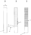
도 1 은 레이저 빔 조사를 통해 판 모양의 작업물 안으로 구멍을 도입하기 위한 다수의 방법단계를 갖는 그리고 판 모양의 작업물 (1) 안으로의 구멍의 도입시 개별적인 방법단계들을 갖는 후속하는 에칭을 갖는 흐름도를 나타낸다. 이를 위해, 도 1 의 (a) 에서 레이저 빔 (2) 은 작업물 (1) 의 표면을 향하여 방향지어진다. 작업물 (1) 의 두께 (d) 는 이때 3 mm 까지이다. 레이저 빔 (2) 의 작용기간은 극도로 짧게 선택되고, 따라서 상기 레이저 빔의 빔축 둘레로 동심적으로 작업물 (1) 의 변조만 생긴다. 이를 위해, 파장을 갖는 레이저가 작동되고, 상기 파장을 위해 작업물 (1) 은 투명하다. 이렇게 변조된, 결손부위들 (3) 을 갖는 영역은 도 1 의 (b) 에 기포들의 선형 사슬의 형태로 도시된다. 다음의, 도 1 의 (c) 에 도시된 방법단계에서, 도시되지 않은 부식시키는 매체의 작용에 근거하여, 먼저 상기 레이저 빔 (2) 을 통해 변조를 겪은, 작업물 (1) 의 결손부위들 (3) 을 통해 형성된 영역들에서 이방성 재료제거가 발생한다. 이를 통해, 원통모양의 작용구역을 따라서, 작업물 (1) 안의 구멍으로서의 컷아웃부 (4) 가 생긴다.Fig. 1 shows a process for preparing a workpiece having a plurality of process steps for introducing holes into a plate-like workpiece through laser beam irradiation and having subsequent etching with individual process steps in the introduction of holes into the plate- Fig. 1 (a), the laser beam 2 is directed toward the surface of the
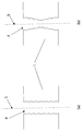
상기 구멍은, 도 2 의 (a) 와 도 2 의 (b) 그리고 도 3 의 (a) 내지 도 3 의 (c) 에서 알아볼 수 있는 바와 같이, 측면 위의 둘러싸는, 동심적인 다수의 구조를 구비한다.As can be seen in Figures 2 (a) and 2 (b) and Figures 3 (a) - 3 (c), the holes may have a number of concentric, Respectively.
이때, 상기 컷아웃부 (4) 는, 에칭공정을 통해 점차적으로, 에칭작용을 통해 작업물 (1) 안의 중공 공간이 되도록 확장되는 상기 먼저 만들어진 결손부위들 (3) 이 연결됨으로써, 상기 나란히 늘어 놓인 다수의 결손부위 (3) 의 상기 점차적인 에칭에 의하여 형성된다. 이를 통해, 에칭 액체는 빨리 한 결손부위 (3) 로부터 다른 결손부위 (3) 에 도달한다. 이때 중력의 영향은 결정적이지 않기 때문에, 에칭 진척은 위로부터 뿐만 아니라 아래로부터도 수행되고, 동시에 두 외면에서 시작된다. 상기 외면들의 영역에서의 상기 부식시키는 매체의 비교적 보다 긴 작용기간을 통해, 도 2 의 (b) 에서 알아볼 수 있는 바와 같이 외부 표면들의 영역에서 결손부위들 (3) 의 원추형 확장부가 발생한다.At this time, the cut-out
변조들로서 작업물 (1) 의 내부에서 만들어지는 결손부위들 (3) 을 통해, 상기 에칭공정은 결손부위들 (3) 이 배치되어 있는 선 (5) 을 따라간다. 선 (5) 은 직선일 수 있고, 또는 상기 에칭공정을 통해 정확히 지켜지는 거의 임의적인 윤곽을 따라갈 수 있다. 이로써, 거의 임의적인 절단윤곽을 만들어내는 것도 처음으로 가능하다.Through the
상기 작업물 안에 멀리 안쪽에 있는 결손부위들 (3) 과 비교하여 상기 외면들을 향한 결손부위들 (3) 의 영역에서의 보다 긴 작용기간을 통해 보다 큰 확장부가 발생할지라도, 그럼에도 불구하고 전체적으로 작은 원뿔모양 확장부가 관찰될 수 있다.Although larger extensions are produced through a longer period of action in the region of the
이렇게 만들어진 상기 컷아웃부 (4) 의 또는 구멍의 윤곽은 상기 에칭공정의 종료 후 횡단면 확장부들과 협착부들의 연속에 의해 특징지어지고, 그들의 형태는 지렁이를 연상시키고, 이때 상기 횡단면 확장부들과 협착부들은, 예컨대 도 2 의 (b) 와 도 3 의 (c) 에서 알아볼 수 있는 바와 같이, 일치하는 횡단면적을 가질 필요도 없고, 도 3 의 (c) 에 도시된 바와 같이, 이웃한 횡단면 확장부들과 협착부들에 대한 일치하는 간격 (a1, a2) 을 가질 필요도 없다. 횡단면 확장부 또는 협착부는 이때 주축에 대한 횡단평면에 배치될 수 있고 또는, 도 3 의 (a) 에 도시된 바와 같이, 그에 대해 기울어져 배치될 수 있다.The contour of the
이웃한 횡단면 확장부들 또는 협착부들은 그 밖에도 중심점들도 구비할 수 있고, 상기 중심점들은 작업물 (1) 의 표면에 대해 기울어진 하나의 공통의 선 (5) 위에 놓여 있고, 따라서 상기 횡단면 확장부들 또는 협착부들은 서로 오프셋되어 배치되고, 이때 상기 횡단면 확장부들 또는 협착부들은 도 3 의 (a) 에 도시된 바와 같이 외면에 대해 기울어져 정렬될 수 있고 또는 도 3 의 (b) 에 도시된 바와 같이 외면에 대해 평행으로 정렬될 수 있다.Neighboring cross-sectional extensions or constrictions may also have other central points which lie on one
도 3 의 (c) 에서 알아볼 수 있는 바와 같이, 이웃한 횡단면 확장부들의 각각의 면적 무게중심들은 오프셋을 구비할 수 있고, 따라서 그들은 특히 하나의 공통의 직선 위에 배치되지 않는다.As can be seen in FIG. 3 (c), the area center-of-gravity centers of each of the neighboring cross-sectional extensions can have offsets, so they are not particularly placed on one common straight line.
Claims (17)
상기 컷아웃부 (4) 및/또는 상기 구멍은 잇따르는 다수의 결손부위 (3) 의 점차적으로 진척되는 에칭에 의하여 형성되는 것을 특징으로 하는, 판 모양의 작업물 안으로 적어도 하나의 컷아웃부 및/또는 구멍을 도입하기 위한 방법.A method for introducing at least one cutout (4) and / or a hole into a plate-like workpiece (1) having a thickness of less than 3 millimeters,
Characterized in that the cutout (4) and / or the hole are formed by gradual progressive etching of a plurality of subsequent defective portions (3), wherein at least one cutout and / Or holes.
결손부위들 (3) 은 하나의 선, 특히 하나의 축 또는 하나의 직선을 따라서 배치되는 것을 특징으로 하는, 판 모양의 작업물 안으로 적어도 하나의 컷아웃부 및/또는 구멍을 도입하기 위한 방법.The method according to claim 1,
A method for introducing at least one cutout and / or hole into a plate-like workpiece, characterized in that the defective portions (3) are arranged along one line, in particular one axis or one straight line.
결손부위들 (3) 은 적어도 일부 섹션들에서 직선 (선 (5)) 에서 벗어나 도입되는 것을 특징으로 하는, 판 모양의 작업물 안으로 적어도 하나의 컷아웃부 및/또는 구멍을 도입하기 위한 방법.The method according to claim 1,
A method for introducing at least one cutout and / or hole into a plate-like workpiece, characterized in that the deficient portions (3) are introduced out of a straight line (line (5)) in at least some sections.
결손부위들 (3) 은 맞닿지 않는 것을 특징으로 하는, 판 모양의 작업물 안으로 적어도 하나의 컷아웃부 및/또는 구멍을 도입하기 위한 방법.4. The method according to any one of claims 1 to 3,
Characterized in that the defective portions (3) are not abutted. ≪ Desc / Clms Page number 13 > 6. A method for introducing at least one cutout and / or hole into a plate-like workpiece.
결손부위들 (3) 은 축 (선 (5)) 을 따라서 한 표면으로부터 제 2 표면까지 연장되는 것을 특징으로 하는, 판 모양의 작업물 안으로 적어도 하나의 컷아웃부 및/또는 구멍을 도입하기 위한 방법.5. The method according to any one of claims 1 to 4,
Characterized in that the deficient portions (3) extend from one surface to the second surface along an axis (line (5)), for introducing at least one cutout and / or hole into the plate- Way.
상기 작업물 (1) 의 평균 두께는 에칭부식을 통해 감소되는 것을 특징으로 하는, 판 모양의 작업물 안으로 적어도 하나의 컷아웃부 및/또는 구멍을 도입하기 위한 방법.6. The method according to any one of claims 1 to 5,
Characterized in that the average thickness of the workpiece (1) is reduced through etching corrosion. ≪ Desc / Clms Page number 13 >
결손부위들 (3) 은 레이저 빔 (2) 과의 상호작용을 통해 생기는 것을 특징으로 하는, 판 모양의 작업물 안으로 적어도 하나의 컷아웃부 및/또는 구멍을 도입하기 위한 방법.7. The method according to any one of claims 1 to 6,
A method for introducing at least one cutout and / or hole into a plate-like workpiece, characterized in that the defective portions (3) are caused by interaction with the laser beam (2).
상기 레이저 빔 (2) 은 파장을 가지며, 상기 파장에 있어서 상기 작업물 (1) 의 재료는 대체로 투명한 것을 특징으로 하는, 판 모양의 작업물 안으로 적어도 하나의 컷아웃부 및/또는 구멍을 도입하기 위한 방법.8. The method according to any one of claims 1 to 7,
Characterized in that the laser beam (2) has a wavelength, and the material of the work (1) at said wavelength is substantially transparent, introducing at least one cutout and / or hole into the plate- Way.
상기 레이저 빔 (2) 은 100 피코세컨드보다 짧은, 특히 12 피코세컨드보다 짧은 펄스길이 (pulse length) 를 갖는 것을 특징으로 하는, 판 모양의 작업물 안으로 적어도 하나의 컷아웃부 및/또는 구멍을 도입하기 위한 방법.9. The method according to any one of claims 1 to 8,
Characterized in that the laser beam (2) has a pulse length shorter than 100 picoseconds, in particular less than 12 picoseconds, introducing at least one cutout and / or hole into the plate-like workpiece Lt; / RTI >
상기 레이저 빔 (2) 은 펄스 형태로 작업물 재료와 상호작용하는 것을 특징으로 하는, 판 모양의 작업물 안으로 적어도 하나의 컷아웃부 및/또는 구멍을 도입하기 위한 방법.10. The method according to any one of claims 1 to 9,
Characterized in that the laser beam (2) interacts with the workpiece material in a pulsed manner.
상기 레이저 빔 (2) 은 펄스 시퀀스 (pulse sequence) 의 형태로 작업물 재료와 상호작용하고, 상기 펄스 시퀀스는 20개를 넘지 않는 단일펄스들을 포함하는 것을 특징으로 하는, 판 모양의 작업물 안으로 적어도 하나의 컷아웃부 및/또는 구멍을 도입하기 위한 방법.11. The method according to any one of claims 1 to 10,
Characterized in that the laser beam (2) interacts with the workpiece material in the form of a pulse sequence and the pulse sequence comprises a single pulse of no more than 20, A method for introducing one cutout and / or a hole.
상기 레이저 빔 (2) 의 초점은 시간적 지연을 통해 빔축을 따라서 상기 작업물 (1) 을 통해 이동하는 것을 특징으로 하는, 판 모양의 작업물 안으로 적어도 하나의 컷아웃부 및/또는 구멍을 도입하기 위한 방법.12. The method according to any one of claims 1 to 11,
Characterized in that the focus of the laser beam (2) is moved through the workpiece (1) along the beam axis through a temporal delay, introducing at least one cutout and / or hole into the plate- Way.
상기 레이저 빔 (2) 의 초점은 공간적 빔형성 (beam forming) 을 통해 작업물 재료의 전체 두께에 걸쳐 빔축을 따라서 상호작용하는 것을 특징으로 하는, 판 모양의 작업물 안으로 적어도 하나의 컷아웃부 및/또는 구멍을 도입하기 위한 방법.13. The method according to any one of claims 1 to 12,
Characterized in that the focal point of the laser beam (2) interacts along the beam axis over the entire thickness of the workpiece material through spatial beam forming, at least one cutout into the plate- / ≪ / RTI >
상기 공간적 빔형성은 강한 구면수차 (spherical aberration) 를 갖는 광학계를 통해 또는 회절 광학 소자를 통해 달성되는 것을 특징으로 하는, 판 모양의 작업물 안으로 적어도 하나의 컷아웃부 및/또는 구멍을 도입하기 위한 방법.14. The method according to any one of claims 1 to 13,
Characterized in that said spatial beam forming is achieved either through an optical system with strong spherical aberration or through a diffractive optical element, characterized in that at least one cutout and / Way.
근축 (paraxial) 광선들의 초점 포인트들 (focus points) 의 위치들과 빔축을 따른 상기 레이저 빔의 주변광선들 사이의 차이는 >100 ㎛ 이고, 특히 바람직하게는 >250 ㎛ 인 것을 특징으로 하는, 판 모양의 작업물 안으로 적어도 하나의 컷아웃부 및/또는 구멍을 도입하기 위한 방법.15. The method according to any one of claims 1 to 14,
Characterized in that the difference between the positions of the focal points of paraxial rays and the peripheral rays of the laser beam along the beam axis is > 100 mu m, particularly preferably > 250 mu m. Shaped workpiece with a cut-out portion and / or a hole.
상기 컷아웃부 (4) 의 또는 구멍의 측면은 지렁이 구조를 형성하는 것을 특징으로 하는, 판 모양의 작업물 안으로 적어도 하나의 컷아웃부 및/또는 구멍을 도입하기 위한 방법.16. The method according to any one of claims 1 to 15,
A method for introducing at least one cutout and / or hole into a plate-like workpiece, characterized in that the or the side of the cutout (4) forms a earthworm structure.
상기 작업물 (1) 의 재료는 본질적인 재료부분으로서 유리, 규소 및/또는 청옥을 구비하는 것을 특징으로 하는, 판 모양의 작업물 안으로 적어도 하나의 컷아웃부 및/또는 구멍을 도입하기 위한 방법.17. The method according to any one of claims 1 to 16,
A method for introducing at least one cutout and / or hole into a plate-like workpiece, characterized in that the material of the workpiece (1) comprises glass, silicon and / or blue sapphire as an essential material part.
Applications Claiming Priority (5)
| Application Number | Priority Date | Filing Date | Title |
|---|---|---|---|
| DE102014113339.0A DE102014113339A1 (en) | 2014-09-16 | 2014-09-16 | Method for producing recesses in a material |
| DE102014113339.0 | 2014-09-16 | ||
| DE102014116291 | 2014-11-07 | ||
| DE102014116291.9 | 2014-11-07 | ||
| PCT/DE2015/100333 WO2016041544A1 (en) | 2014-09-16 | 2015-08-07 | Method for introducing at least one cutout or aperture into a sheetlike workpiece |
Related Child Applications (1)
| Application Number | Title | Priority Date | Filing Date |
|---|---|---|---|
| KR1020197015976A Division KR20190065480A (en) | 2014-09-16 | 2015-08-07 | Method for introducing at least one cutout or aperture into a sheetlike workpiece |
Publications (1)
| Publication Number | Publication Date |
|---|---|
| KR20170044143A true KR20170044143A (en) | 2017-04-24 |
Family
ID=54072638
Family Applications (4)
| Application Number | Title | Priority Date | Filing Date |
|---|---|---|---|
| KR1020217005121A KR20210022773A (en) | 2014-09-16 | 2015-08-07 | Method for introducing at least one cutout or aperture into a sheetlike workpiece |
| KR1020177007041A KR20170044143A (en) | 2014-09-16 | 2015-08-07 | Method for introducing at least one cutout or aperture into a sheetlike workpiece |
| KR1020237018486A KR20230084606A (en) | 2014-09-16 | 2015-08-07 | Method for introducing at least one cutout or aperture into a sheetlike workpiece |
| KR1020197015976A KR20190065480A (en) | 2014-09-16 | 2015-08-07 | Method for introducing at least one cutout or aperture into a sheetlike workpiece |
Family Applications Before (1)
| Application Number | Title | Priority Date | Filing Date |
|---|---|---|---|
| KR1020217005121A KR20210022773A (en) | 2014-09-16 | 2015-08-07 | Method for introducing at least one cutout or aperture into a sheetlike workpiece |
Family Applications After (2)
| Application Number | Title | Priority Date | Filing Date |
|---|---|---|---|
| KR1020237018486A KR20230084606A (en) | 2014-09-16 | 2015-08-07 | Method for introducing at least one cutout or aperture into a sheetlike workpiece |
| KR1020197015976A KR20190065480A (en) | 2014-09-16 | 2015-08-07 | Method for introducing at least one cutout or aperture into a sheetlike workpiece |
Country Status (11)
| Country | Link |
|---|---|
| US (2) | US11610784B2 (en) |
| EP (2) | EP4061101A1 (en) |
| JP (2) | JP6782692B2 (en) |
| KR (4) | KR20210022773A (en) |
| CN (1) | CN107006128B (en) |
| ES (1) | ES2923764T3 (en) |
| LT (1) | LT3195706T (en) |
| MY (1) | MY196621A (en) |
| SG (2) | SG10201902331XA (en) |
| TW (1) | TWI616939B (en) |
| WO (1) | WO2016041544A1 (en) |
Families Citing this family (14)
| Publication number | Priority date | Publication date | Assignee | Title |
|---|---|---|---|---|
| DE102018100299A1 (en) * | 2017-01-27 | 2018-08-02 | Schott Ag | Structured plate-shaped glass element and method for its production |
| CN110382160B (en) | 2017-03-06 | 2022-09-27 | Lpkf激光电子股份公司 | Method for opening at least one recess into a material by means of electromagnetic radiation and a subsequent etching process |
| KR102481312B1 (en) | 2017-03-06 | 2022-12-23 | 엘피케이에프 레이저 앤드 일렉트로닉스 악티엔게젤샤프트 | Method for producing a technical mask |
| DE102018110211A1 (en) * | 2018-04-27 | 2019-10-31 | Schott Ag | Method for producing fine structures in the volume of a substrate made of brittle-hard material |
| TWI678342B (en) | 2018-11-09 | 2019-12-01 | 財團法人工業技術研究院 | Cutting method for forming chamfered corners |
| DE102020100848B4 (en) | 2019-01-29 | 2023-07-27 | Lpkf Laser & Electronics Aktiengesellschaft | Process for microstructuring a glass substrate using laser radiation |
| DE102019201347B3 (en) * | 2019-02-01 | 2020-06-18 | Lpkf Laser & Electronics Ag | Manufacture of metallic conductor tracks on glass |
| DE102019121827A1 (en) * | 2019-08-13 | 2021-02-18 | Trumpf Laser- Und Systemtechnik Gmbh | Laser etching with varying etching selectivity |
| CN113594014B (en) * | 2020-04-30 | 2024-04-12 | 中微半导体设备(上海)股份有限公司 | Component, plasma reaction device, and component processing method |
| DE102020114195A1 (en) | 2020-05-27 | 2021-12-02 | Lpkf Laser & Electronics Aktiengesellschaft | Method for making a recess in a substrate |
| CN111799169A (en) * | 2020-07-17 | 2020-10-20 | 绍兴同芯成集成电路有限公司 | Process for processing TGV by combining femtosecond laser with HF wet etching |
| DE102021204675B4 (en) | 2021-05-07 | 2023-05-17 | Lpkf Laser & Electronics Se | Device and method for cell cultivation |
| CN113510364B (en) * | 2021-07-28 | 2022-11-25 | 广东工业大学 | Forming method of three-dimensional cavity structure based on laser-assisted dissolution |
| EP4296244A1 (en) | 2022-06-21 | 2023-12-27 | LPKF Laser & Electronics SE | Substrate carrier made of glass for processing a substrate and a method for producing the same |
Citations (2)
| Publication number | Priority date | Publication date | Assignee | Title |
|---|---|---|---|---|
| WO2012014720A1 (en) * | 2010-07-26 | 2012-02-02 | 浜松ホトニクス株式会社 | Laser processing method |
| WO2012014718A1 (en) * | 2010-07-26 | 2012-02-02 | 浜松ホトニクス株式会社 | Method for manufacturing interposer |
Family Cites Families (17)
| Publication number | Priority date | Publication date | Assignee | Title |
|---|---|---|---|---|
| WO2001015819A1 (en) * | 1999-08-30 | 2001-03-08 | Board Of Regents University Of Nebraska-Lincoln | Three-dimensional electrical interconnects |
| JP4880820B2 (en) | 2001-01-19 | 2012-02-22 | 株式会社レーザーシステム | Laser assisted machining method |
| JP4418282B2 (en) | 2004-03-31 | 2010-02-17 | 株式会社レーザーシステム | Laser processing method |
| JP4222296B2 (en) | 2004-11-22 | 2009-02-12 | 住友電気工業株式会社 | Laser processing method and laser processing apparatus |
| US9138913B2 (en) | 2005-09-08 | 2015-09-22 | Imra America, Inc. | Transparent material processing with an ultrashort pulse laser |
| JP2011218398A (en) * | 2010-04-08 | 2011-11-04 | Fujikura Ltd | Method for forming microstructure, laser irradiation device, and substrate |
| DE102010025966B4 (en) | 2010-07-02 | 2012-03-08 | Schott Ag | Interposer and method for making holes in an interposer |
| CN103079747B (en) * | 2010-07-12 | 2016-08-03 | 罗芬-西纳技术有限公司 | The method being carried out material process by laser filament effect |
| US9108269B2 (en) * | 2010-07-26 | 2015-08-18 | Hamamatsu Photonics K. K. | Method for manufacturing light-absorbing substrate and method for manufacturing mold for making same |
| US8933367B2 (en) | 2011-02-09 | 2015-01-13 | Sumitomo Electric Industries, Ltd. | Laser processing method |
| WO2014085663A1 (en) | 2012-11-29 | 2014-06-05 | Corning Incorporated | Methods of fabricating glass articles by laser damage and etching |
| EP2754524B1 (en) | 2013-01-15 | 2015-11-25 | Corning Laser Technologies GmbH | Method of and apparatus for laser based processing of flat substrates being wafer or glass element using a laser beam line |
| JP6113529B2 (en) * | 2013-03-05 | 2017-04-12 | 株式会社ディスコ | Wafer processing method |
| DE102013223637B4 (en) | 2013-11-20 | 2018-02-01 | Trumpf Laser- Und Systemtechnik Gmbh | A method of treating a laser transparent substrate for subsequently separating the substrate |
| US9517963B2 (en) | 2013-12-17 | 2016-12-13 | Corning Incorporated | Method for rapid laser drilling of holes in glass and products made therefrom |
| CN110049956A (en) * | 2016-11-04 | 2019-07-23 | 康宁公司 | Microperforated panel system, application and the method for manufacturing microperforated panel system |
| US11344973B2 (en) * | 2018-04-19 | 2022-05-31 | Corning Incorporated | Methods for forming holes in substrates |
-
2015
- 2015-08-07 KR KR1020217005121A patent/KR20210022773A/en not_active IP Right Cessation
- 2015-08-07 ES ES15762474T patent/ES2923764T3/en active Active
- 2015-08-07 LT LTEPPCT/DE2015/100333T patent/LT3195706T/en unknown
- 2015-08-07 KR KR1020177007041A patent/KR20170044143A/en active Application Filing
- 2015-08-07 SG SG10201902331XA patent/SG10201902331XA/en unknown
- 2015-08-07 EP EP22167179.5A patent/EP4061101A1/en active Pending
- 2015-08-07 SG SG11201702091WA patent/SG11201702091WA/en unknown
- 2015-08-07 JP JP2017512917A patent/JP6782692B2/en active Active
- 2015-08-07 CN CN201580049903.1A patent/CN107006128B/en active Active
- 2015-08-07 KR KR1020237018486A patent/KR20230084606A/en not_active Application Discontinuation
- 2015-08-07 MY MYPI2017700845A patent/MY196621A/en unknown
- 2015-08-07 WO PCT/DE2015/100333 patent/WO2016041544A1/en active Application Filing
- 2015-08-07 KR KR1020197015976A patent/KR20190065480A/en not_active IP Right Cessation
- 2015-08-07 US US15/511,272 patent/US11610784B2/en active Active
- 2015-08-07 EP EP15762474.3A patent/EP3195706B1/en active Active
- 2015-09-09 TW TW104129751A patent/TWI616939B/en active
-
2020
- 2020-07-09 JP JP2020118488A patent/JP7049404B2/en active Active
-
2022
- 2022-04-01 US US17/711,136 patent/US20220223434A1/en active Pending
Patent Citations (2)
| Publication number | Priority date | Publication date | Assignee | Title |
|---|---|---|---|---|
| WO2012014720A1 (en) * | 2010-07-26 | 2012-02-02 | 浜松ホトニクス株式会社 | Laser processing method |
| WO2012014718A1 (en) * | 2010-07-26 | 2012-02-02 | 浜松ホトニクス株式会社 | Method for manufacturing interposer |
Also Published As
| Publication number | Publication date |
|---|---|
| TWI616939B (en) | 2018-03-01 |
| JP7049404B2 (en) | 2022-04-06 |
| US20220223434A1 (en) | 2022-07-14 |
| JP6782692B2 (en) | 2020-11-11 |
| JP2017534458A (en) | 2017-11-24 |
| JP2020185613A (en) | 2020-11-19 |
| KR20190065480A (en) | 2019-06-11 |
| MY196621A (en) | 2023-04-23 |
| US11610784B2 (en) | 2023-03-21 |
| CN107006128A (en) | 2017-08-01 |
| US20170256422A1 (en) | 2017-09-07 |
| LT3195706T (en) | 2022-08-10 |
| EP4061101A1 (en) | 2022-09-21 |
| KR20230084606A (en) | 2023-06-13 |
| WO2016041544A1 (en) | 2016-03-24 |
| TW201621986A (en) | 2016-06-16 |
| ES2923764T3 (en) | 2022-09-30 |
| SG10201902331XA (en) | 2019-04-29 |
| EP3195706B1 (en) | 2022-06-01 |
| CN107006128B (en) | 2020-05-19 |
| SG11201702091WA (en) | 2017-04-27 |
| EP3195706A1 (en) | 2017-07-26 |
| KR20210022773A (en) | 2021-03-03 |
Similar Documents
| Publication | Publication Date | Title |
|---|---|---|
| KR20170044143A (en) | Method for introducing at least one cutout or aperture into a sheetlike workpiece | |
| KR101857336B1 (en) | Method and device for separating a substrate | |
| US11148225B2 (en) | Method for rapid laser drilling of holes in glass and products made therefrom | |
| JP6186016B2 (en) | Method and apparatus for drilling through holes in a substrate | |
| CN110382160A (en) | For at least one recessed to be spaced apart the method being set in material by electromagnetic radiation and subsequent etching process | |
| JP2020109820A (en) | Laser processing method for printed circuit board and laser processing machine for printed circuit board | |
| JP2023523031A (en) | Method for generating recesses in a substrate | |
| WO2022026348A1 (en) | High boron oxide low alumina and alkali-free glasses for through glass via applications | |
| JP6238675B2 (en) | Laser processing method and inkjet head manufacturing method |
Legal Events
| Date | Code | Title | Description |
|---|---|---|---|
| A201 | Request for examination | ||
| AMND | Amendment | ||
| E902 | Notification of reason for refusal | ||
| AMND | Amendment | ||
| E601 | Decision to refuse application | ||
| AMND | Amendment | ||
| A107 | Divisional application of patent | ||
| J201 | Request for trial against refusal decision | ||
| J301 | Trial decision |
Free format text: TRIAL NUMBER: 2019101001861; TRIAL DECISION FOR APPEAL AGAINST DECISION TO DECLINE REFUSAL REQUESTED 20190603 Effective date: 20191210 |