EP2597767B1 - Inverter device and air conditioner including the same - Google Patents
Inverter device and air conditioner including the same Download PDFInfo
- Publication number
- EP2597767B1 EP2597767B1 EP12190706.7A EP12190706A EP2597767B1 EP 2597767 B1 EP2597767 B1 EP 2597767B1 EP 12190706 A EP12190706 A EP 12190706A EP 2597767 B1 EP2597767 B1 EP 2597767B1
- Authority
- EP
- European Patent Office
- Prior art keywords
- switching element
- switching
- circuit
- inverter device
- resistor
- Prior art date
- Legal status (The legal status is an assumption and is not a legal conclusion. Google has not performed a legal analysis and makes no representation as to the accuracy of the status listed.)
- Active
Links
Images
Classifications
-
- H—ELECTRICITY
- H02—GENERATION; CONVERSION OR DISTRIBUTION OF ELECTRIC POWER
- H02M—APPARATUS FOR CONVERSION BETWEEN AC AND AC, BETWEEN AC AND DC, OR BETWEEN DC AND DC, AND FOR USE WITH MAINS OR SIMILAR POWER SUPPLY SYSTEMS; CONVERSION OF DC OR AC INPUT POWER INTO SURGE OUTPUT POWER; CONTROL OR REGULATION THEREOF
- H02M5/00—Conversion of ac power input into ac power output, e.g. for change of voltage, for change of frequency, for change of number of phases
- H02M5/02—Conversion of ac power input into ac power output, e.g. for change of voltage, for change of frequency, for change of number of phases without intermediate conversion into dc
- H02M5/04—Conversion of ac power input into ac power output, e.g. for change of voltage, for change of frequency, for change of number of phases without intermediate conversion into dc by static converters
- H02M5/22—Conversion of ac power input into ac power output, e.g. for change of voltage, for change of frequency, for change of number of phases without intermediate conversion into dc by static converters using discharge tubes with control electrode or semiconductor devices with control electrode
- H02M5/275—Conversion of ac power input into ac power output, e.g. for change of voltage, for change of frequency, for change of number of phases without intermediate conversion into dc by static converters using discharge tubes with control electrode or semiconductor devices with control electrode using devices of a triode or transistor type requiring continuous application of a control signal
- H02M5/297—Conversion of ac power input into ac power output, e.g. for change of voltage, for change of frequency, for change of number of phases without intermediate conversion into dc by static converters using discharge tubes with control electrode or semiconductor devices with control electrode using devices of a triode or transistor type requiring continuous application of a control signal for conversion of frequency
-
- H—ELECTRICITY
- H02—GENERATION; CONVERSION OR DISTRIBUTION OF ELECTRIC POWER
- H02M—APPARATUS FOR CONVERSION BETWEEN AC AND AC, BETWEEN AC AND DC, OR BETWEEN DC AND DC, AND FOR USE WITH MAINS OR SIMILAR POWER SUPPLY SYSTEMS; CONVERSION OF DC OR AC INPUT POWER INTO SURGE OUTPUT POWER; CONTROL OR REGULATION THEREOF
- H02M1/00—Details of apparatus for conversion
- H02M1/08—Circuits specially adapted for the generation of control voltages for semiconductor devices incorporated in static converters
- H02M1/088—Circuits specially adapted for the generation of control voltages for semiconductor devices incorporated in static converters for the simultaneous control of series or parallel connected semiconductor devices
-
- H—ELECTRICITY
- H03—ELECTRONIC CIRCUITRY
- H03K—PULSE TECHNIQUE
- H03K17/00—Electronic switching or gating, i.e. not by contact-making and –breaking
- H03K17/12—Modifications for increasing the maximum permissible switched current
- H03K17/127—Modifications for increasing the maximum permissible switched current in composite switches
-
- H—ELECTRICITY
- H03—ELECTRONIC CIRCUITRY
- H03K—PULSE TECHNIQUE
- H03K17/00—Electronic switching or gating, i.e. not by contact-making and –breaking
- H03K17/16—Modifications for eliminating interference voltages or currents
- H03K17/161—Modifications for eliminating interference voltages or currents in field-effect transistor switches
- H03K17/162—Modifications for eliminating interference voltages or currents in field-effect transistor switches without feedback from the output circuit to the control circuit
- H03K17/163—Soft switching
-
- H—ELECTRICITY
- H02—GENERATION; CONVERSION OR DISTRIBUTION OF ELECTRIC POWER
- H02M—APPARATUS FOR CONVERSION BETWEEN AC AND AC, BETWEEN AC AND DC, OR BETWEEN DC AND DC, AND FOR USE WITH MAINS OR SIMILAR POWER SUPPLY SYSTEMS; CONVERSION OF DC OR AC INPUT POWER INTO SURGE OUTPUT POWER; CONTROL OR REGULATION THEREOF
- H02M1/00—Details of apparatus for conversion
- H02M1/0048—Circuits or arrangements for reducing losses
-
- H—ELECTRICITY
- H03—ELECTRONIC CIRCUITRY
- H03K—PULSE TECHNIQUE
- H03K2217/00—Indexing scheme related to electronic switching or gating, i.e. not by contact-making or -breaking covered by H03K17/00
- H03K2217/0036—Means reducing energy consumption
-
- Y—GENERAL TAGGING OF NEW TECHNOLOGICAL DEVELOPMENTS; GENERAL TAGGING OF CROSS-SECTIONAL TECHNOLOGIES SPANNING OVER SEVERAL SECTIONS OF THE IPC; TECHNICAL SUBJECTS COVERED BY FORMER USPC CROSS-REFERENCE ART COLLECTIONS [XRACs] AND DIGESTS
- Y02—TECHNOLOGIES OR APPLICATIONS FOR MITIGATION OR ADAPTATION AGAINST CLIMATE CHANGE
- Y02B—CLIMATE CHANGE MITIGATION TECHNOLOGIES RELATED TO BUILDINGS, e.g. HOUSING, HOUSE APPLIANCES OR RELATED END-USER APPLICATIONS
- Y02B70/00—Technologies for an efficient end-user side electric power management and consumption
- Y02B70/10—Technologies improving the efficiency by using switched-mode power supplies [SMPS], i.e. efficient power electronics conversion e.g. power factor correction or reduction of losses in power supplies or efficient standby modes
Definitions
- the present invention relates to an inverter device and an air conditioner including the inverter device.
- International Patent Publication No. 2000-072433 discloses a technology for realizing a reduction in an energization loss of an entire switching circuit by configuring, as a switching circuit included in an inverter device, a parallel circuit in which a Si transistor and a non-Si transistor including a SiC or GaN semiconductor are connected in parallel and for realizing a reduction in a switching loss by simultaneously raising a gate voltage of the Si transistor and a gate voltage of the non-Si transistor.
- International Patent Publication No. 2001-020757 discloses a technology for reducing a conduction loss and a switching loss by connecting in parallel a main transistor including a current-driven semiconductor switching element having a small conduction loss and an auxiliary transistor including a voltage-driven semiconductor element having switching speed higher than that of the current-driven semiconductor switching element to configure a main switch and turning on the auxiliary transistor earlier than the main transistor and turning off the auxiliary transistor later than the main transistor.
- the switching circuit is turned on by the non-Si transistor including the SiC or GaN semiconductor element having high switching speed during turn-on. Therefore, the non-Si transistor having a large current capacity needs to be used. As a result, the price of the non-Si transistor more expensive than the Si semiconductor element further rises.
- driving signals for driving the main transistor and the auxiliary transistor are supplied independently from each other. Therefore, when the inverter device is configured, driving signals twice as many as normal driving signals are necessary. As a result, a driving control circuit cannot be configured using a general-purpose device and the price of the driving control circuit rises.
- JP H09 172359 A discloses a technique for improving current balance between plural switching elements (chips) which are connected in parallel. In order to suppress concentration of current on a part of the plural switching elements and thus improve the current balance between the plural switching elements, the ON/OFF timings of the respective switching elements are aligned with each other.
- EP 1 028 528 A1 shows a switching regulator comprising a first switching element and a second switching element connected in parallel with the first switching element and having an on-resistance smaller than that of the first switching element.
- a pulse generating circuit is configured to turn on the second switching element later than the first switching element and to turn off the first switching element later than the second switching element, this configuration serves to reduce switching noise.
- US 2009/179688 A1 relates to a semiconductor integrated circuit for controlling a transition of a plurality of switch transistors, which are used for supplying power to a plurality of circuit cells and cutting off the supply of power to the circuit cells, from a turned-off state to a turned-on state and relates to a power-supply control method for controlling such a transition.
- the present invention has been devised in view of the above and it is an object of the present invention to provide an inverter device that can realize a further reduction in costs while enjoying a loss reduction effect and an air conditioner including the inverter device.
- an inverter device including: a rectifying circuit configured to rectify an alternating-current voltage output from an alternating-current power supply into a direct-current voltage; a smoothing capacitor configured to smooth the direct-current voltage rectified by the rectifying circuit; a converting circuit configured to convert the direct-current voltage smoothed by the smoothing capacitor into a desired alternating-current voltage; and a control unit configured to control the converting circuit, wherein the converting circuit includes a plurality of switching circuits each including: a first switching element; and a second switching element connecting in parallel with the first switching element, having a conduction loss smaller than that of the first switching element and having switching speed higher than that of the first switching element, and the control unit includes: a driving unit configured to generate a plurality of driving signals for respectively driving the switching circuits to be turned on and off; and a gate circuit configured to, for each of the switching circuits, based on the driving signals, turn on the second switching element later than the first switching element and turn off the first switching element later than the second switching element
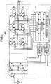
- FIG.1 is a diagram of a configuration example of an inverter device according to a first embodiment.
- an inverter device 100 includes a reactor 2 for power factor improvement, a diode bridge (a rectifying circuit) 3 that rectifies an alternating-current voltage output from an alternating-current power supply 1 via the reactor 2, a smoothing capacitor 6 that smoothes a direct-current voltage rectified by the diode bridge 3, a converting circuit 4 that converts the direct-current voltage smoothed by the smoothing capacitor 6 into a desired alternating-current voltage, a current detecting unit 13 that detects an electric current flowing to a resistor 11 to thereby detect a circuit current flowing to the converting circuit 4, a voltage detecting unit 14 that detects a voltage across both ends of the smoothing capacitor 6 to thereby detect a direct-current voltage applied to the converting circuit 4, and a control unit 200 that controls the converting circuit 4.
- a reactor 2 for power factor improvement includes a reactor 2 for power factor improvement, a diode bridge (a rectifying
- the diode bridge 3 includes diodes 3a, 3b, 3c, and 3d.
- the smoothing capacitor 6 includes smoothing capacitors 6a and 6b connected in series.
- the smoothing capacitor 6 is configured to be capable of switching full-wave rectification and half-wave rectification according to an open and close state of a switch 7 connected between one end of the alternating-current power supply 1 and a middle point of the smoothing capacitors 6a and 6b.
- the alternating-current power supply 1 is a single-phase alternating-current supply.
- the alternating-current power supply 1 is not limited to this and can be a three-phase alternating-current power supply. In this case, the diode bridge 3 only has to be configured to rectify a three-phase alternating-current voltage.
- a three-phase motor 12 is driven as a load of the converting circuit 4.
- the converting circuit 4 is configured by connecting, for each of phases, two switching circuits 5 in series via the resistor 11 between a positive electrode side and a negative electrode side of the smoothing capacitor 6.
- the configuration of the converting circuit 4 is not limited to this.
- the converting circuit 4 can be configured to drive a single-phase motor.
- the converting circuit 4 includes a plurality of switching circuits 5 in which first switching elements 8, second switching elements 9, and freewheeling diodes 10 are connected in parallel.
- the first switching element 8 for example, a voltage-driven semiconductor element such as an IGBT or a MOSFET including a silicon (Si) semiconductor is used.
- a voltage-driven semiconductor element such as an IGBT or a MOSFET including a wideband gap (hereinafter referred to as "WBG") semiconductor such as silicon carbide (SiC) or gallium nitride (GaN) material or diamond is used.
- the second switching element 9 including the WBG semiconductor has a characteristic that ON resistance is smaller than that of the first switching element 8 including the Si semiconductor and switching speed is higher than that of the first switching element 8.
- the control unit 200 includes a PWM-signal generating unit 15, a driving unit 16, and a gate circuit 17.
- the PWM-signal generating unit 15 performs motor driving control using pulse width modulation (PWM).
- PWM pulse width modulation
- the PWM-signal generating unit 15 generates PWM signals, which are the source of driving signals for driving the switching circuits 5, based on a circuit current flowing to the converting circuit 4 detected by the current detecting unit 13 and a direct-current voltage applied to the converting circuit 4 detected by the voltage detecting unit 14.
- the driving unit 16 generates, based on the PWM signals, the driving signals for driving the switching circuits 5 and outputs the driving signals to the gate circuit 17.
- the PWM-signal generating unit 15 and the driving unit 16 can be different devices or can be configured as one device.
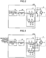
- FIG.2 is diagram of a configuration example of the gate circuit in the inverter device according to the first embodiment.
- the gate circuit 17 includes, for each of the switching circuits 5, a first diode 61 and a first resistor 51 connected in series in a direction in which an electric current flows from the driving unit 16 to a gate terminal (a control terminal) of the first switching element 8, a second diode 62 and a second resistor 52 connected in series in a direction in which an electric current flows from the gate terminal of the first switching element 8 to the driving unit 16, a third diode 63 and a third resistor 53 connected in series in a direction in which an electric current flows from the driving unit 16 to a gate terminal of the second switching element 9, and a fourth diode 64 and a fourth resistor 54 connected in series in a direction in which an electric current flows from the gate terminal of the second switching element 9 to
- one driving signal is input to the gate circuit 17 for the switching circuits 5 in which the first switching elements 8 and the second switching elements 9 are connected in parallel. In other words, it is unnecessary to independently supply a driving signal to each of the first switching elements 8 and the second switching elements 9 of the switching circuits 5. Therefore, it is possible to configure the PWM-signal generating unit 15 and the driving unit 16 using an inexpensive general-purpose device.
- the first switching element 8 and the second switching element 9 have parasitic capacitances between gate terminals and collector terminals (input terminals: in the case of a MOSFET, drain terminals). Therefore, during rising of a driving signal input to the gate circuit 17, a time constant circuit of the first resistor 51 and the parasitic capacitance between the gate and the collector of the first switching element 8 and a time constant circuit of the third resistor 53 and the parasitic capacitance between the gate and the collector of the second switching element 9 are configured.
- the resistance of the first resistor 51 is set to a value smaller than the resistance of the third resistor 53. Therefore, the first switching element 8 is turned on earlier and the second switching element 9 is turned on later.
- a time constant circuit of the second resistor 52 and the parasitic capacitance between the gate and the collector of the first switching element 8 and a time constant of the fourth resistor 54 and the parasitic capacitance between the gate and the collector of the second switching element 9 are configured.
- the resistance of the second resistor 52 is set to a value larger than the resistor of the fourth resistor 54. Therefore, the first switching element 8 is turned on later than the second switching element 9.
- the switching circuit 5 is turned on and off by the first switching element 8.
- the second switching element 9 is turned on and off in a state in which the first switching element 8 is off. Therefore, a switching loss by the second switching element 9 is extremely small. Therefore, even if the second switching element 9 is configured by an expensive WBG semiconductor, a device having a small current capacity can be used. Consequently, costs can be reduced to be smaller than costs required when a converting circuit is configured using only a switching element including the WBG semiconductor.
- the switching circuit 5 is turned on and off by the first switching element 8 including the Si semiconductor. Therefore, a switching loss is larger than a switching loss that occurs when the converting circuit is configured by using only the switching element including the WBG semiconductor.
- the switching loss is equivalent to a switching loss that occurs when a converting circuit is configured by using only a switching element including the Si semiconductor.
- the second switching element 9 including the WBG semiconductor is on, most of an electric current flowing in the switching circuit 5 flows to the second switching element 9. Therefore, a conduction loss can be reduced to be smaller than a conduction loss that occurs when the converting circuit is configured by using only the switching element including the Si semiconductor.
- the first switching element and the second switching element having the ON resistance smaller than that of the first switching element and having the switching speed higher than that of the first switching element are connected in parallel to configure the switching circuit.
- the second switching element is turned on later than the first switching element.
- the first switching element is turned off later than the second switching element. Therefore, because the second switching element is turned on and off in a state in which the first switching element is off, a switching loss by the second switching element is extremely small. Therefore, even when the second switching element includes the expensive WBG semiconductor, a device having small current capacity can be used. Consequently, costs can be reduced to be smaller than costs required when the converting circuit is configured by using only the switching element including the WBG semiconductor.
- switching noise that occurs during turn-on and during turn-off of the switching element increases.
- turn-on and turn-off of the switching element are carried out by the first switching element including the Si semiconductor having the switching speed lower than that of the second switching element including the WBG semiconductor. Therefore, switching noise can be further suppressed than switching noise that occurs when the converting circuit is configured by using only the switching element including the WBG semiconductor.
- the switching circuits in which the first switching elements and the second switching elements are connected in parallel are driven by one driving signal. Therefore, it is unnecessary to independently supply a driving signal to each of the first switching elements and the second switching elements of the switching circuits. Consequently, it is possible to configure the PWM-signal generating unit and the driving unit using an inexpensive general-purpose device.
- the switching circuit is turned on and off by the first switching element including the Si semiconductor. Therefore, a switching loss is larger than a switching loss that occurs when the converting circuit is configured by using only the switching element including the WBG semiconductor.
- the switching loss is equivalent to a switching loss that occurs when the converting circuit is configured by using only the switching element including the Si semiconductor.
- a conduction loss can be reduced to be smaller than a conduction loss that occurs when the converting circuit is configured by using only the switching element including the Si semiconductor.
- the low-load state means, for example, a state in which a compressor motor is actuated with a low load different from a load during a normal operation of the compressor motor, for example, when a dormant refrigerant in the compressor motor under suspension is prevented by restrictively energizing a motor winding to prevent the compressor motor connected as a load of a converting circuit from rotating.
- FIG.3 is a diagram of a configuration example of a gate circuit in an inverter device according to the second embodiment.
- An overall configuration of the inverter device 100 according to the second embodiment is the same as that of the inverter device according to the first embodiment. Therefore, components same as or equivalent to those in the first embodiment are denoted by the same reference numerals and signs and detailed explanation of the components is omitted.
- a control unit 200a of the inverter device 100 includes, instead of the gate circuit 17 explained in the first embodiment, a gate circuit 17a further including a transistor 18 that causes a short-circuit between a gate terminal and an emitter terminal (an output terminal: a source terminal in the case of a MOSFET) of the first switching element 8.
- control unit 200a controls the transistor 18 in the gate circuit 17a to be turned on and causes a short-circuit between the gate terminal and the emitter terminal of the first switching element 8.
- the control unit 200a thereby stops turning on and off the first switching element 8 and turns on and off only the second switching element 9.
- a carrier frequency in PWM control can be set higher than that in the normal time. Therefore, noise caused by a motor during the restrictive energization can be removed from an audible band by stopping the first switching element 8 being turned on and off and setting the carrier frequency of the PWM signal higher than that during the normal operation (e.g., equal to or higher than 20 kilohertz). Further, a magnetic flux generated in the motor winding can be intensified by setting the carrier frequency high. Therefore, it is possible to not only heat the motor winding but also heat a core of the motor with the magnetic flux generated in the motor winding.
- the inverter device when the load connected to the converting circuit is in the low-load state different from the state in the normal time, the first switching element is stopped being turned on and off and only the second switching element having ON resistance smaller than that of the first switching element and having switching speed higher than that of the first switching element is turned on and off. Therefore, it is possible to further reduce a switching loss and a conduction loss of the switching circuit in the low-load state.
- the carrier frequency in the PWM control can be set higher than that in the normal time.
- the switching circuit when the switching circuit is used for a rotational operation of the compressor motor, in carrying out the restrictive energization of the compressor motor, noise caused by the motor during the restrictive energization can be removed from the audible band by setting the carrier frequency of the PWM signal higher than that during the normal operation (e.g., equal to or higher than 20 kilohertz).
- a magnetic flux generated in the motor winding can be intensified by setting the carrier frequency high. Therefore, it is possible to not only heat the motor winding but also heat the core of the motor with the magnetic flux generated in the motor winding.
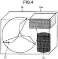
- FIG.4 is a configuration schematic diagram of an outdoor unit of the air conditioner according to the third embodiment.
- an outdoor unit 30 of the air conditioner according to the third embodiment includes a fan 31 for facilitating heat exchange between an outdoor heat exchanger (not shown in the figure) and the outdoor air, a compressor 32 that circulates a compressed refrigerant to a refrigerant circuit (not shown in the figure) in the air conditioner, and the inverter device 100 according to the first or second embodiment.
- the inverter device 100 is set in an upper part of the outdoor unit 30.
- the inverter device 100 controls a rotational operation of a compressor motor included in the compressor 32.
- the inverter device 100 is not limited to be used for the control of the rotational operation of the compressor motor included in the compressor 32.
- the inverter device 100 may control a rotational operation of a motor that drives the fan 31 and a ventilation fan (not shown in the figure) in the indoor unit (not shown in the figure).
- the first switching element and the second switching element having the ON resistance smaller than that of the first switching element and having the switching speed higher than that of the first switching element are connected in parallel to configure the switching circuit.
- the second switching element is turned on later than the first switching element.
- the first switching element is turned off later than the second switching element. Therefore, even when the second switching element is configured to include the expensive WBG semiconductor, a device having small current capacity can be used. Consequently, costs can be reduced compared with costs of an inverter device in which only the switching element including the WBG semiconductor is used.
- the switching circuits in which the first switching elements and the second switching elements are connected in parallel are driven by one driving signal. Therefore, the control unit or the driving unit can be configured using an inexpensive general-purpose device. Consequently, it is possible to reduce costs to be smaller than costs required when the inverter device having the same configuration including the two switching elements connected in parallel is used.
- the switching circuit is turned on and off by the first switching element including the Si semiconductor. Therefore, a switching loss is equivalent to a switching loss caused when the inverter device including the converting circuit configured by using only the switching element including the Si semiconductor is used. However, in a period in which the second switching element including the WBG semiconductor is on, most of an electric current flowing in the switching circuit flows to the second switching element. Therefore, a conduction loss can be reduced to be smaller than a conduction loss caused when the inverter device including the converting circuit configured by using only the switching element including the Si semiconductor is used.
- the inverter device explained in the second embodiment is applied to the air conditioner, when the load connected to the converting circuit is in the low-load state different from the state in the normal time, the first switching element is stopped being turned on and off and only the second switching element having ON resistance smaller than that of the first switching element and having switching speed higher than that of the first switching element is turned on and off. Therefore, it is possible to further reduce a loss in the low-load state to be smaller than a loss in the low-load state caused when the inverter device having the same configuration including the two switching elements connected in parallel is used.
- the carrier frequency in the PWM control can be set higher than that in the normal time. Therefore, when the restrictive energization of the compressor motor is carried out, noise caused by the motor during the restrictive energization can be removed from the audible band by setting the carrier frequency of the PWM signal higher than that during the normal operation (e.g., equal to or higher than 20 kilohertz). Further, a magnetic flux generated in the motor winding can be intensified by setting the carrier frequency high. Therefore, it is possible to not only heat the motor winding but also heat the core of the motor with the magnetic flux generated in the motor winding. Consequently, it is possible to efficiently prevent a dormant refrigerant in the compressor motor under suspension.
- the switching element including the WBG semiconductor has a high withstanding voltage and a high allowable current density. Therefore, it is possible to reduce the size of switching elements. By using the switching elements reduced in the size, it is possible to reduce the size of an inverter circuit incorporating the elements.
- the switching element including the WBG semiconductor has high heat resistance as well. Therefore, because a heat radiation fin of a heat sink can be reduced in size, it is possible to further reduce the size of an inverter circuit.
Description
- The present invention relates to an inverter device and an air conditioner including the inverter device.
- In the past, for example, International Patent Publication No.
2000-072433 discloses a technology for realizing a reduction in an energization loss of an entire switching circuit by configuring, as a switching circuit included in an inverter device, a parallel circuit in which a Si transistor and a non-Si transistor including a SiC or GaN semiconductor are connected in parallel and for realizing a reduction in a switching loss by simultaneously raising a gate voltage of the Si transistor and a gate voltage of the non-Si transistor. - Further, for example, International Patent Publication No.
2001-020757 discloses a technology for reducing a conduction loss and a switching loss by connecting in parallel a main transistor including a current-driven semiconductor switching element having a small conduction loss and an auxiliary transistor including a voltage-driven semiconductor element having switching speed higher than that of the current-driven semiconductor switching element to configure a main switch and turning on the auxiliary transistor earlier than the main transistor and turning off the auxiliary transistor later than the main transistor. - However, in the technology disclosed in International Patent Publication No.
2000-072433 2001-020757 -
JP H09 172359 A -
EP 1 028 528 A1 shows a switching regulator comprising a first switching element and a second switching element connected in parallel with the first switching element and having an on-resistance smaller than that of the first switching element. A pulse generating circuit is configured to turn on the second switching element later than the first switching element and to turn off the first switching element later than the second switching element, this configuration serves to reduce switching noise. -
US 2009/179688 A1 relates to a semiconductor integrated circuit for controlling a transition of a plurality of switch transistors, which are used for supplying power to a plurality of circuit cells and cutting off the supply of power to the circuit cells, from a turned-off state to a turned-on state and relates to a power-supply control method for controlling such a transition. - The present invention has been devised in view of the above and it is an object of the present invention to provide an inverter device that can realize a further reduction in costs while enjoying a loss reduction effect and an air conditioner including the inverter device.
- It is an object of the present invention to at least partially solve the problems in the conventional technology.
- There is provided an inverter device including: a rectifying circuit configured to rectify an alternating-current voltage output from an alternating-current power supply into a direct-current voltage; a smoothing capacitor configured to smooth the direct-current voltage rectified by the rectifying circuit; a converting circuit configured to convert the direct-current voltage smoothed by the smoothing capacitor into a desired alternating-current voltage; and a control unit configured to control the converting circuit, wherein the converting circuit includes a plurality of switching circuits each including: a first switching element; and a second switching element connecting in parallel with the first switching element, having a conduction loss smaller than that of the first switching element and having switching speed higher than that of the first switching element, and the control unit includes: a driving unit configured to generate a plurality of driving signals for respectively driving the switching circuits to be turned on and off; and a gate circuit configured to, for each of the switching circuits, based on the driving signals, turn on the second switching element later than the first switching element and turn off the first switching element later than the second switching element, wherein the gate circuit includes, for each of the switching circuits: a first diode and a first resistor connected in series in a direction in which an electric current flows from the driving unit to a control terminal of the first switching element; a second diode and a second resistor connected in series in a direction in which an electric current flows from the control terminal of the first switching element to the driving unit; a third diode and a third resistor connected in series in a direction in which an electric current flows from the driving unit to a control terminal of the second switching element; wherein a fourth diode and a fourth resistor connected in series in a direction in which an electric current flows from the control terminal of the second switching circuit to the driving unit, and resistance of the first resistor is smaller than resistance of the third resistor, and resistance of the second resistor is larger than resistance of the fourth resistor.
- The above and other objects, features, advantages and technical and industrial significance of this invention will be better understood by reading the following detailed description of presently preferred embodiments of the invention, when considered in connection with the accompanying drawings.
-
-
FIG.1 is a diagram of a configuration example of an inverter device according to a first embodiment; -
FIG.2 is a diagram of a configuration example of a gate circuit in the inverter device according to the first embodiment; -
FIG.3 is a diagram of a configuration example of a gate circuit in an inverter device according to a second embodiment; and -
FIG.4 is a configuration schematic diagram of an outdoor unit of an air conditioner according to a third embodiment. - An inverter device and an air conditioner including the inverter device according to embodiments of the present invention are explained below with reference to the accompanying drawings. The present invention is not limited by the embodiments explained below.
-
FIG.1 is a diagram of a configuration example of an inverter device according to a first embodiment. As shown inFIG.1 , aninverter device 100 according to the first embodiment includes areactor 2 for power factor improvement, a diode bridge (a rectifying circuit) 3 that rectifies an alternating-current voltage output from an alternating-current power supply 1 via thereactor 2, a smoothingcapacitor 6 that smoothes a direct-current voltage rectified by thediode bridge 3, a convertingcircuit 4 that converts the direct-current voltage smoothed by the smoothingcapacitor 6 into a desired alternating-current voltage, a current detectingunit 13 that detects an electric current flowing to aresistor 11 to thereby detect a circuit current flowing to the convertingcircuit 4, avoltage detecting unit 14 that detects a voltage across both ends of the smoothingcapacitor 6 to thereby detect a direct-current voltage applied to the convertingcircuit 4, and acontrol unit 200 that controls the convertingcircuit 4. - The
diode bridge 3 includesdiodes FIG.1 , the smoothingcapacitor 6 includes smoothingcapacitors capacitor 6 is configured to be capable of switching full-wave rectification and half-wave rectification according to an open and close state of a switch 7 connected between one end of the alternating-current power supply 1 and a middle point of the smoothingcapacitors FIG.1 , the alternating-current power supply 1 is a single-phase alternating-current supply. However, the alternating-current power supply 1 is not limited to this and can be a three-phase alternating-current power supply. In this case, thediode bridge 3 only has to be configured to rectify a three-phase alternating-current voltage. - In the example shown in
FIG.1 , a three-phase motor 12 is driven as a load of the convertingcircuit 4. In this case, the convertingcircuit 4 is configured by connecting, for each of phases, two switchingcircuits 5 in series via theresistor 11 between a positive electrode side and a negative electrode side of the smoothingcapacitor 6. The configuration of the convertingcircuit 4 is not limited to this. The convertingcircuit 4 can be configured to drive a single-phase motor. - The converting
circuit 4 includes a plurality of switchingcircuits 5 in whichfirst switching elements 8,second switching elements 9, and freewheelingdiodes 10 are connected in parallel. - In this embodiment, as the
first switching element 8, for example, a voltage-driven semiconductor element such as an IGBT or a MOSFET including a silicon (Si) semiconductor is used. As thesecond switching element 9, for example, a voltage-driven semiconductor element such as an IGBT or a MOSFET including a wideband gap (hereinafter referred to as "WBG") semiconductor such as silicon carbide (SiC) or gallium nitride (GaN) material or diamond is used. Thesecond switching element 9 including the WBG semiconductor has a characteristic that ON resistance is smaller than that of thefirst switching element 8 including the Si semiconductor and switching speed is higher than that of thefirst switching element 8. - The
control unit 200 includes a PWM-signal generating unit 15, a drivingunit 16, and agate circuit 17. - The PWM-
signal generating unit 15 performs motor driving control using pulse width modulation (PWM). In this embodiment, the PWM-signal generating unit 15 generates PWM signals, which are the source of driving signals for driving theswitching circuits 5, based on a circuit current flowing to the convertingcircuit 4 detected by the current detectingunit 13 and a direct-current voltage applied to the convertingcircuit 4 detected by thevoltage detecting unit 14. - The driving
unit 16 generates, based on the PWM signals, the driving signals for driving theswitching circuits 5 and outputs the driving signals to thegate circuit 17. The PWM-signal generating unit 15 and the drivingunit 16 can be different devices or can be configured as one device. - The
gate circuit 17 turns on and off thefirst switching elements 8 and thesecond switching elements 9 in theswitching circuits 5 based on the driving signals.FIG.2 is diagram of a configuration example of the gate circuit in the inverter device according to the first embodiment. As shown inFIG.2 , thegate circuit 17 includes, for each of the switchingcircuits 5, afirst diode 61 and afirst resistor 51 connected in series in a direction in which an electric current flows from the drivingunit 16 to a gate terminal (a control terminal) of thefirst switching element 8, asecond diode 62 and asecond resistor 52 connected in series in a direction in which an electric current flows from the gate terminal of thefirst switching element 8 to the drivingunit 16, athird diode 63 and athird resistor 53 connected in series in a direction in which an electric current flows from the drivingunit 16 to a gate terminal of thesecond switching element 9, and a fourth diode 64 and a fourth resistor 54 connected in series in a direction in which an electric current flows from the gate terminal of thesecond switching element 9 to the drivingunit 16. In this embodiment, the resistance of thefirst resistor 51 is set to a value smaller than the resistance of thethird resistor 53. The resistance of thesecond resistor 52 is set to a value larger than the resistance of the fourth resistor 54. - The operation of the
switching circuits 5 in theinverter device 100 according to the first embodiment is explained. - In this embodiment, one driving signal is input to the
gate circuit 17 for theswitching circuits 5 in which thefirst switching elements 8 and thesecond switching elements 9 are connected in parallel. In other words, it is unnecessary to independently supply a driving signal to each of thefirst switching elements 8 and thesecond switching elements 9 of theswitching circuits 5. Therefore, it is possible to configure the PWM-signal generatingunit 15 and thedriving unit 16 using an inexpensive general-purpose device. - The
first switching element 8 and thesecond switching element 9 have parasitic capacitances between gate terminals and collector terminals (input terminals: in the case of a MOSFET, drain terminals). Therefore, during rising of a driving signal input to thegate circuit 17, a time constant circuit of thefirst resistor 51 and the parasitic capacitance between the gate and the collector of thefirst switching element 8 and a time constant circuit of thethird resistor 53 and the parasitic capacitance between the gate and the collector of thesecond switching element 9 are configured. In this embodiment, the resistance of thefirst resistor 51 is set to a value smaller than the resistance of thethird resistor 53. Therefore, thefirst switching element 8 is turned on earlier and thesecond switching element 9 is turned on later. - On the other hand, during falling of the driving signal input to the
gate circuit 17, a time constant circuit of thesecond resistor 52 and the parasitic capacitance between the gate and the collector of thefirst switching element 8 and a time constant of the fourth resistor 54 and the parasitic capacitance between the gate and the collector of thesecond switching element 9 are configured. In this embodiment, the resistance of thesecond resistor 52 is set to a value larger than the resistor of the fourth resistor 54. Therefore, thefirst switching element 8 is turned on later than thesecond switching element 9. - In other words, the switching
circuit 5 is turned on and off by thefirst switching element 8. Thesecond switching element 9 is turned on and off in a state in which thefirst switching element 8 is off. Therefore, a switching loss by thesecond switching element 9 is extremely small. Therefore, even if thesecond switching element 9 is configured by an expensive WBG semiconductor, a device having a small current capacity can be used. Consequently, costs can be reduced to be smaller than costs required when a converting circuit is configured using only a switching element including the WBG semiconductor. - The
switching circuit 5 is turned on and off by thefirst switching element 8 including the Si semiconductor. Therefore, a switching loss is larger than a switching loss that occurs when the converting circuit is configured by using only the switching element including the WBG semiconductor. The switching loss is equivalent to a switching loss that occurs when a converting circuit is configured by using only a switching element including the Si semiconductor. However, in a period in which thesecond switching element 9 including the WBG semiconductor is on, most of an electric current flowing in theswitching circuit 5 flows to thesecond switching element 9. Therefore, a conduction loss can be reduced to be smaller than a conduction loss that occurs when the converting circuit is configured by using only the switching element including the Si semiconductor. - As explained above, with the inverter device according to the first embodiment, the first switching element and the second switching element having the ON resistance smaller than that of the first switching element and having the switching speed higher than that of the first switching element are connected in parallel to configure the switching circuit. The second switching element is turned on later than the first switching element. The first switching element is turned off later than the second switching element. Therefore, because the second switching element is turned on and off in a state in which the first switching element is off, a switching loss by the second switching element is extremely small. Therefore, even when the second switching element includes the expensive WBG semiconductor, a device having small current capacity can be used. Consequently, costs can be reduced to be smaller than costs required when the converting circuit is configured by using only the switching element including the WBG semiconductor.
- In general, when a switching element having high switching speed is used, switching noise that occurs during turn-on and during turn-off of the switching element increases. However, in this embodiment, turn-on and turn-off of the switching element are carried out by the first switching element including the Si semiconductor having the switching speed lower than that of the second switching element including the WBG semiconductor. Therefore, switching noise can be further suppressed than switching noise that occurs when the converting circuit is configured by using only the switching element including the WBG semiconductor.
- The switching circuits in which the first switching elements and the second switching elements are connected in parallel are driven by one driving signal. Therefore, it is unnecessary to independently supply a driving signal to each of the first switching elements and the second switching elements of the switching circuits. Consequently, it is possible to configure the PWM-signal generating unit and the driving unit using an inexpensive general-purpose device.
- The switching circuit is turned on and off by the first switching element including the Si semiconductor. Therefore, a switching loss is larger than a switching loss that occurs when the converting circuit is configured by using only the switching element including the WBG semiconductor. The switching loss is equivalent to a switching loss that occurs when the converting circuit is configured by using only the switching element including the Si semiconductor. However, in a period in which the second switching element including the WBG semiconductor is on, most of an electric current flowing in the switching circuit flows to the second switching element. Therefore, a conduction loss can be reduced to be smaller than a conduction loss that occurs when the converting circuit is configured by using only the switching element including the Si semiconductor.
- In an example explained in a second embodiment, only a second switching element including a WBG semiconductor is turned on and off in a low-load state. The low-load state means, for example, a state in which a compressor motor is actuated with a low load different from a load during a normal operation of the compressor motor, for example, when a dormant refrigerant in the compressor motor under suspension is prevented by restrictively energizing a motor winding to prevent the compressor motor connected as a load of a converting circuit from rotating.
-
FIG.3 is a diagram of a configuration example of a gate circuit in an inverter device according to the second embodiment. An overall configuration of theinverter device 100 according to the second embodiment is the same as that of the inverter device according to the first embodiment. Therefore, components same as or equivalent to those in the first embodiment are denoted by the same reference numerals and signs and detailed explanation of the components is omitted. - As shown in
FIG.3 , acontrol unit 200a of theinverter device 100 according to the second embodiment includes, instead of thegate circuit 17 explained in the first embodiment, agate circuit 17a further including atransistor 18 that causes a short-circuit between a gate terminal and an emitter terminal (an output terminal: a source terminal in the case of a MOSFET) of thefirst switching element 8. - An operation performed when a load connected to the converting
circuit 4 is in a low-load state different from a state in normal time in theinverter device 100 according to the second embodiment is explained. In the following explanation, as an example of the operation performed when the load connected to the convertingcircuit 4 is in the low-load state different from the state in the normal time, restrictive energization of the three-phase motor 12 for compressor driving is carried out. - When a restrictive energization operation command is input from the outside, the
control unit 200a controls thetransistor 18 in thegate circuit 17a to be turned on and causes a short-circuit between the gate terminal and the emitter terminal of thefirst switching element 8. Thecontrol unit 200a thereby stops turning on and off thefirst switching element 8 and turns on and off only thesecond switching element 9. - When the load connected to the converting
circuit 4 is in the low-load state different from the state in the normal time, for example, when the restrictive energization of the three-phase motor 12 is carried out, an electric current flowing to theswitching circuits 5 is smaller than that in the normal time. Therefore, only the second switching element having small ON resistance and high switching speed is turned on and off. Consequently, it is possible to further reduce a switching loss and a conduction loss of theswitching circuit 5. - Because the switching loss is reduced, a carrier frequency in PWM control can be set higher than that in the normal time. Therefore, noise caused by a motor during the restrictive energization can be removed from an audible band by stopping the
first switching element 8 being turned on and off and setting the carrier frequency of the PWM signal higher than that during the normal operation (e.g., equal to or higher than 20 kilohertz). Further, a magnetic flux generated in the motor winding can be intensified by setting the carrier frequency high. Therefore, it is possible to not only heat the motor winding but also heat a core of the motor with the magnetic flux generated in the motor winding. - As explained above, with the inverter device according to the second embodiment, when the load connected to the converting circuit is in the low-load state different from the state in the normal time, the first switching element is stopped being turned on and off and only the second switching element having ON resistance smaller than that of the first switching element and having switching speed higher than that of the first switching element is turned on and off. Therefore, it is possible to further reduce a switching loss and a conduction loss of the switching circuit in the low-load state.
- Because the switching loss of the switching circuit is reduced, the carrier frequency in the PWM control can be set higher than that in the normal time. For example, when the switching circuit is used for a rotational operation of the compressor motor, in carrying out the restrictive energization of the compressor motor, noise caused by the motor during the restrictive energization can be removed from the audible band by setting the carrier frequency of the PWM signal higher than that during the normal operation (e.g., equal to or higher than 20 kilohertz). Further, a magnetic flux generated in the motor winding can be intensified by setting the carrier frequency high. Therefore, it is possible to not only heat the motor winding but also heat the core of the motor with the magnetic flux generated in the motor winding.
- In an example explained in a third embodiment, the inverter device explained in the first and second embodiments is applied to an air conditioner.
FIG.4 is a configuration schematic diagram of an outdoor unit of the air conditioner according to the third embodiment. - As shown in
FIG.4 , anoutdoor unit 30 of the air conditioner according to the third embodiment includes afan 31 for facilitating heat exchange between an outdoor heat exchanger (not shown in the figure) and the outdoor air, acompressor 32 that circulates a compressed refrigerant to a refrigerant circuit (not shown in the figure) in the air conditioner, and theinverter device 100 according to the first or second embodiment. - In the example shown in
FIG.4 , theinverter device 100 is set in an upper part of theoutdoor unit 30. Theinverter device 100 controls a rotational operation of a compressor motor included in thecompressor 32. Theinverter device 100 is not limited to be used for the control of the rotational operation of the compressor motor included in thecompressor 32. For example, theinverter device 100 may control a rotational operation of a motor that drives thefan 31 and a ventilation fan (not shown in the figure) in the indoor unit (not shown in the figure). - As explained above, with the air conditioner according to the third embodiment, because the inverter device explained in the first embodiment is applied, the first switching element and the second switching element having the ON resistance smaller than that of the first switching element and having the switching speed higher than that of the first switching element are connected in parallel to configure the switching circuit. The second switching element is turned on later than the first switching element. The first switching element is turned off later than the second switching element. Therefore, even when the second switching element is configured to include the expensive WBG semiconductor, a device having small current capacity can be used. Consequently, costs can be reduced compared with costs of an inverter device in which only the switching element including the WBG semiconductor is used.
- The switching circuits in which the first switching elements and the second switching elements are connected in parallel are driven by one driving signal. Therefore, the control unit or the driving unit can be configured using an inexpensive general-purpose device. Consequently, it is possible to reduce costs to be smaller than costs required when the inverter device having the same configuration including the two switching elements connected in parallel is used.
- The switching circuit is turned on and off by the first switching element including the Si semiconductor. Therefore, a switching loss is equivalent to a switching loss caused when the inverter device including the converting circuit configured by using only the switching element including the Si semiconductor is used. However, in a period in which the second switching element including the WBG semiconductor is on, most of an electric current flowing in the switching circuit flows to the second switching element. Therefore, a conduction loss can be reduced to be smaller than a conduction loss caused when the inverter device including the converting circuit configured by using only the switching element including the Si semiconductor is used.
- Because the inverter device explained in the second embodiment is applied to the air conditioner, when the load connected to the converting circuit is in the low-load state different from the state in the normal time, the first switching element is stopped being turned on and off and only the second switching element having ON resistance smaller than that of the first switching element and having switching speed higher than that of the first switching element is turned on and off. Therefore, it is possible to further reduce a loss in the low-load state to be smaller than a loss in the low-load state caused when the inverter device having the same configuration including the two switching elements connected in parallel is used.
- For example, when the inverter device explained in the second embodiment is applied to the rotational operation of the compressor motor, the carrier frequency in the PWM control can be set higher than that in the normal time. Therefore, when the restrictive energization of the compressor motor is carried out, noise caused by the motor during the restrictive energization can be removed from the audible band by setting the carrier frequency of the PWM signal higher than that during the normal operation (e.g., equal to or higher than 20 kilohertz). Further, a magnetic flux generated in the motor winding can be intensified by setting the carrier frequency high. Therefore, it is possible to not only heat the motor winding but also heat the core of the motor with the magnetic flux generated in the motor winding. Consequently, it is possible to efficiently prevent a dormant refrigerant in the compressor motor under suspension.
- Effects obtained by using the switching element including the WBG semiconductor explained in the embodiments are not limited to the effects described in the embodiments.
- For example, the switching element including the WBG semiconductor has a high withstanding voltage and a high allowable current density. Therefore, it is possible to reduce the size of switching elements. By using the switching elements reduced in the size, it is possible to reduce the size of an inverter circuit incorporating the elements.
- The switching element including the WBG semiconductor has high heat resistance as well. Therefore, because a heat radiation fin of a heat sink can be reduced in size, it is possible to further reduce the size of an inverter circuit.
- According to the present invention, there is an effect that it is possible to realize a further reduction in costs while enjoying a loss reduction effect.
- Although the invention has been described with respect to specific embodiments for a complete and clear disclosure, the appended claims are not to be thus limited but are to be construed as embodying all modifications and alternative constructions that may occur to one skilled in the art that fairly fall within the basic teaching herein set forth.
Claims (6)
- An inverter device (100) comprising:a rectifying circuit (3) configured to rectify an alternating-current voltage output from an alternating-current power supply (1) into a direct-current voltage;a smoothing capacitor (6, 6a, 6b) configured to smooth the direct-current voltage rectified by the rectifying circuit (3);a converting circuit (4) configured to convert the direct-current voltage smoothed by the smoothing capacitor (6, 6a, 6b) into a desired alternating-current voltage; anda control unit (200, 200a) configured to control the converting circuit (4), whereinthe converting circuit (4) includes a plurality of switching circuits (5) each including:a first switching element (8); anda second switching element (9) connected in parallel with the first switching element (8), having a conduction loss smaller than that of the first switching element (8) and having switching speed higher than that of the first switching element (8), andthe control unit (200, 200a) includes:characterized in that
a driving unit (16) configured to generate a plurality of driving signals for respectively driving the switching circuits (5) to be turned on and off,the inverter device (100) further comprises:
a gate circuit (17, 17a) configured to, for each of the switching circuits (5), based on the driving signals, turn on the second switching element (9) later than the first switching element (8) and turn off the first switching element (8) later than the second switching element (9), whereinthe gate circuit (17, 17a) includes, for each of the switching circuits:a first diode (61) and a first resistor (51) connected in series in a direction in which an electric current flows from the driving unit (16) to a control terminal of the first switching element (8);a second diode (62) and a second resistor (52) connected in series in a direction in which an electric current flows from the control terminal of the first switching element (8) to the driving unit (16);a third diode (63) and a third resistor (53) connected in series in a direction in which an electric current flows from the driving unit (16) to a control terminal of the second switching element (9); whereina fourth diode (64) and a fourth resistor (54) connected in series in a direction in which an electric current flows from the control terminal of the second switching circuit (9) to the driving unit (16), andresistance of the first resistor (51) is smaller than resistance of the third resistor (53), and resistance of the second resistor (52) is larger than resistance of the fourth resistor (54). - The inverter device (100) according to claim 1, wherein the control unit (200, 200a) stops the first switching element (8) being turned on and off when a load of the converting circuit (4) is in a low-load state different from a state in normal time.
- The inverter device (100) according to claim 1, whereinthe gate circuit (17, 17a) further includes, for each of the switching circuits (5), a plurality of transistors configured to cause a short-circuit between the control terminal and an output terminal of the first switching element (8), andthe control unit(200, 200a) controls the transistor to be turned on when a load of the converting circuit (4) is in a low-load state different from a state in normal time.
- The inverter device (100) according to any one of claims 1 to 3, wherein the second switching element (9) is formed by a wideband gap semiconductor.
- The inverter device (100) according to claim 4, wherein the wideband gap semiconductor is a silicon carbide or gallium nitride material or diamond.
- An air conditioner comprising:one inverter device (100) or a plurality of the inverter devices (100) according to any one of claims 1 to 5;an indoor unit including a ventilation fan configured to send out cooled or warmed air into a room; andan outdoor unit (30) including a compressor (32) configured to compress a refrigerant, a heat exchanger configured to carry out heat exchange between the refrigerant and outdoor air, and a fan (31) configured to send the outdoor air into the heat exchanger, whereinone motor or a plurality of motors among motors configured to drive the ventilation fan (31), the compressor (32), or the fan (31) are driven to rotate by the one inverter device (100) or the plurality of inverter devices (100) corresponding thereto.
Applications Claiming Priority (1)
| Application Number | Priority Date | Filing Date | Title |
|---|---|---|---|
| JP2011257386A JP5591213B2 (en) | 2011-11-25 | 2011-11-25 | Inverter device and air conditioner equipped with the same |
Publications (3)
| Publication Number | Publication Date |
|---|---|
| EP2597767A2 EP2597767A2 (en) | 2013-05-29 |
| EP2597767A3 EP2597767A3 (en) | 2014-08-06 |
| EP2597767B1 true EP2597767B1 (en) | 2018-08-22 |
Family
ID=47290617
Family Applications (1)
| Application Number | Title | Priority Date | Filing Date |
|---|---|---|---|
| EP12190706.7A Active EP2597767B1 (en) | 2011-11-25 | 2012-10-31 | Inverter device and air conditioner including the same |
Country Status (6)
| Country | Link |
|---|---|
| US (1) | US8884560B2 (en) |
| EP (1) | EP2597767B1 (en) |
| JP (1) | JP5591213B2 (en) |
| CN (1) | CN103138596B (en) |
| AU (1) | AU2012254876B2 (en) |
| ES (1) | ES2689796T3 (en) |
Cited By (1)
| Publication number | Priority date | Publication date | Assignee | Title |
|---|---|---|---|---|
| CN107143966A (en) * | 2017-03-21 | 2017-09-08 | 深圳达实智能股份有限公司 | The control method and device of Hospital Central Air-conditioning System magnetic suspension cold water main unit |
Families Citing this family (279)
| Publication number | Priority date | Publication date | Assignee | Title |
|---|---|---|---|---|
| US20070084897A1 (en) | 2003-05-20 | 2007-04-19 | Shelton Frederick E Iv | Articulating surgical stapling instrument incorporating a two-piece e-beam firing mechanism |
| US9060770B2 (en) | 2003-05-20 | 2015-06-23 | Ethicon Endo-Surgery, Inc. | Robotically-driven surgical instrument with E-beam driver |
| US11896225B2 (en) | 2004-07-28 | 2024-02-13 | Cilag Gmbh International | Staple cartridge comprising a pan |
| US10159482B2 (en) | 2005-08-31 | 2018-12-25 | Ethicon Llc | Fastener cartridge assembly comprising a fixed anvil and different staple heights |
| US11246590B2 (en) | 2005-08-31 | 2022-02-15 | Cilag Gmbh International | Staple cartridge including staple drivers having different unfired heights |
| US7934630B2 (en) | 2005-08-31 | 2011-05-03 | Ethicon Endo-Surgery, Inc. | Staple cartridges for forming staples having differing formed staple heights |
| US11484312B2 (en) | 2005-08-31 | 2022-11-01 | Cilag Gmbh International | Staple cartridge comprising a staple driver arrangement |
| US7669746B2 (en) | 2005-08-31 | 2010-03-02 | Ethicon Endo-Surgery, Inc. | Staple cartridges for forming staples having differing formed staple heights |
| US20070106317A1 (en) | 2005-11-09 | 2007-05-10 | Shelton Frederick E Iv | Hydraulically and electrically actuated articulation joints for surgical instruments |
| US11278279B2 (en) | 2006-01-31 | 2022-03-22 | Cilag Gmbh International | Surgical instrument assembly |
| US8186555B2 (en) | 2006-01-31 | 2012-05-29 | Ethicon Endo-Surgery, Inc. | Motor-driven surgical cutting and fastening instrument with mechanical closure system |
| US7845537B2 (en) | 2006-01-31 | 2010-12-07 | Ethicon Endo-Surgery, Inc. | Surgical instrument having recording capabilities |
| US20120292367A1 (en) | 2006-01-31 | 2012-11-22 | Ethicon Endo-Surgery, Inc. | Robotically-controlled end effector |
| US8820603B2 (en) | 2006-01-31 | 2014-09-02 | Ethicon Endo-Surgery, Inc. | Accessing data stored in a memory of a surgical instrument |
| US20110290856A1 (en) | 2006-01-31 | 2011-12-01 | Ethicon Endo-Surgery, Inc. | Robotically-controlled surgical instrument with force-feedback capabilities |
| US7753904B2 (en) | 2006-01-31 | 2010-07-13 | Ethicon Endo-Surgery, Inc. | Endoscopic surgical instrument with a handle that can articulate with respect to the shaft |
| US11793518B2 (en) | 2006-01-31 | 2023-10-24 | Cilag Gmbh International | Powered surgical instruments with firing system lockout arrangements |
| US8708213B2 (en) | 2006-01-31 | 2014-04-29 | Ethicon Endo-Surgery, Inc. | Surgical instrument having a feedback system |
| US8992422B2 (en) | 2006-03-23 | 2015-03-31 | Ethicon Endo-Surgery, Inc. | Robotically-controlled endoscopic accessory channel |
| US10568652B2 (en) | 2006-09-29 | 2020-02-25 | Ethicon Llc | Surgical staples having attached drivers of different heights and stapling instruments for deploying the same |
| US11291441B2 (en) | 2007-01-10 | 2022-04-05 | Cilag Gmbh International | Surgical instrument with wireless communication between control unit and remote sensor |
| US8684253B2 (en) | 2007-01-10 | 2014-04-01 | Ethicon Endo-Surgery, Inc. | Surgical instrument with wireless communication between a control unit of a robotic system and remote sensor |
| US8652120B2 (en) | 2007-01-10 | 2014-02-18 | Ethicon Endo-Surgery, Inc. | Surgical instrument with wireless communication between control unit and sensor transponders |
| US8540128B2 (en) | 2007-01-11 | 2013-09-24 | Ethicon Endo-Surgery, Inc. | Surgical stapling device with a curved end effector |
| US8727197B2 (en) | 2007-03-15 | 2014-05-20 | Ethicon Endo-Surgery, Inc. | Staple cartridge cavity configuration with cooperative surgical staple |
| US11564682B2 (en) | 2007-06-04 | 2023-01-31 | Cilag Gmbh International | Surgical stapler device |
| US8931682B2 (en) | 2007-06-04 | 2015-01-13 | Ethicon Endo-Surgery, Inc. | Robotically-controlled shaft based rotary drive systems for surgical instruments |
| US11849941B2 (en) | 2007-06-29 | 2023-12-26 | Cilag Gmbh International | Staple cartridge having staple cavities extending at a transverse angle relative to a longitudinal cartridge axis |
| US8636736B2 (en) | 2008-02-14 | 2014-01-28 | Ethicon Endo-Surgery, Inc. | Motorized surgical cutting and fastening instrument |
| US7866527B2 (en) | 2008-02-14 | 2011-01-11 | Ethicon Endo-Surgery, Inc. | Surgical stapling apparatus with interlockable firing system |
| US9179912B2 (en) | 2008-02-14 | 2015-11-10 | Ethicon Endo-Surgery, Inc. | Robotically-controlled motorized surgical cutting and fastening instrument |
| US7819298B2 (en) | 2008-02-14 | 2010-10-26 | Ethicon Endo-Surgery, Inc. | Surgical stapling apparatus with control features operable with one hand |
| RU2493788C2 (en) | 2008-02-14 | 2013-09-27 | Этикон Эндо-Серджери, Инк. | Surgical cutting and fixing instrument, which has radio-frequency electrodes |
| US9005230B2 (en) | 2008-09-23 | 2015-04-14 | Ethicon Endo-Surgery, Inc. | Motorized surgical instrument |
| US8210411B2 (en) | 2008-09-23 | 2012-07-03 | Ethicon Endo-Surgery, Inc. | Motor-driven surgical cutting instrument |
| US9386983B2 (en) | 2008-09-23 | 2016-07-12 | Ethicon Endo-Surgery, Llc | Robotically-controlled motorized surgical instrument |
| US11648005B2 (en) | 2008-09-23 | 2023-05-16 | Cilag Gmbh International | Robotically-controlled motorized surgical instrument with an end effector |
| US8608045B2 (en) | 2008-10-10 | 2013-12-17 | Ethicon Endo-Sugery, Inc. | Powered surgical cutting and stapling apparatus with manually retractable firing system |
| US11925354B2 (en) | 2010-09-30 | 2024-03-12 | Cilag Gmbh International | Staple cartridge comprising staples positioned within a compressible portion thereof |
| US9629814B2 (en) | 2010-09-30 | 2017-04-25 | Ethicon Endo-Surgery, Llc | Tissue thickness compensator configured to redistribute compressive forces |
| US9839420B2 (en) | 2010-09-30 | 2017-12-12 | Ethicon Llc | Tissue thickness compensator comprising at least one medicament |
| US9861361B2 (en) | 2010-09-30 | 2018-01-09 | Ethicon Llc | Releasable tissue thickness compensator and fastener cartridge having the same |
| US11812965B2 (en) | 2010-09-30 | 2023-11-14 | Cilag Gmbh International | Layer of material for a surgical end effector |
| US9295464B2 (en) | 2010-09-30 | 2016-03-29 | Ethicon Endo-Surgery, Inc. | Surgical stapler anvil comprising a plurality of forming pockets |
| US11298125B2 (en) | 2010-09-30 | 2022-04-12 | Cilag Gmbh International | Tissue stapler having a thickness compensator |
| US10945731B2 (en) | 2010-09-30 | 2021-03-16 | Ethicon Llc | Tissue thickness compensator comprising controlled release and expansion |
| US9320523B2 (en) | 2012-03-28 | 2016-04-26 | Ethicon Endo-Surgery, Llc | Tissue thickness compensator comprising tissue ingrowth features |
| US8695866B2 (en) | 2010-10-01 | 2014-04-15 | Ethicon Endo-Surgery, Inc. | Surgical instrument having a power control circuit |
| RU2606493C2 (en) | 2011-04-29 | 2017-01-10 | Этикон Эндо-Серджери, Инк. | Staple cartridge, containing staples, located inside its compressible part |
| US9072535B2 (en) | 2011-05-27 | 2015-07-07 | Ethicon Endo-Surgery, Inc. | Surgical stapling instruments with rotatable staple deployment arrangements |
| CN104334098B (en) | 2012-03-28 | 2017-03-22 | 伊西康内外科公司 | Tissue thickness compensator comprising capsules defining a low pressure environment |
| CN104321024B (en) | 2012-03-28 | 2017-05-24 | 伊西康内外科公司 | Tissue thickness compensator comprising a plurality of layers |
| US9101358B2 (en) | 2012-06-15 | 2015-08-11 | Ethicon Endo-Surgery, Inc. | Articulatable surgical instrument comprising a firing drive |
| US20140001231A1 (en) | 2012-06-28 | 2014-01-02 | Ethicon Endo-Surgery, Inc. | Firing system lockout arrangements for surgical instruments |
| BR112014032776B1 (en) | 2012-06-28 | 2021-09-08 | Ethicon Endo-Surgery, Inc | SURGICAL INSTRUMENT SYSTEM AND SURGICAL KIT FOR USE WITH A SURGICAL INSTRUMENT SYSTEM |
| US9408606B2 (en) | 2012-06-28 | 2016-08-09 | Ethicon Endo-Surgery, Llc | Robotically powered surgical device with manually-actuatable reversing system |
| US9649111B2 (en) | 2012-06-28 | 2017-05-16 | Ethicon Endo-Surgery, Llc | Replaceable clip cartridge for a clip applier |
| US9289256B2 (en) | 2012-06-28 | 2016-03-22 | Ethicon Endo-Surgery, Llc | Surgical end effectors having angled tissue-contacting surfaces |
| MX364729B (en) | 2013-03-01 | 2019-05-06 | Ethicon Endo Surgery Inc | Surgical instrument with a soft stop. |
| RU2672520C2 (en) | 2013-03-01 | 2018-11-15 | Этикон Эндо-Серджери, Инк. | Hingedly turnable surgical instruments with conducting ways for signal transfer |
| US9629629B2 (en) | 2013-03-14 | 2017-04-25 | Ethicon Endo-Surgey, LLC | Control systems for surgical instruments |
| US9867612B2 (en) | 2013-04-16 | 2018-01-16 | Ethicon Llc | Powered surgical stapler |
| BR112015026109B1 (en) | 2013-04-16 | 2022-02-22 | Ethicon Endo-Surgery, Inc | surgical instrument |
| DE102013107239B3 (en) * | 2013-07-09 | 2014-03-20 | Semikron Elektronik Gmbh & Co. Kg | Power semiconductor circuit |
| RU2678363C2 (en) | 2013-08-23 | 2019-01-28 | ЭТИКОН ЭНДО-СЕРДЖЕРИ, ЭлЭлСи | Firing member retraction devices for powered surgical instruments |
| US9510828B2 (en) | 2013-08-23 | 2016-12-06 | Ethicon Endo-Surgery, Llc | Conductor arrangements for electrically powered surgical instruments with rotatable end effectors |
| JP2015171226A (en) * | 2014-03-06 | 2015-09-28 | 三菱電機株式会社 | inverter device and air conditioner |
| US10013049B2 (en) | 2014-03-26 | 2018-07-03 | Ethicon Llc | Power management through sleep options of segmented circuit and wake up control |
| BR112016023807B1 (en) | 2014-04-16 | 2022-07-12 | Ethicon Endo-Surgery, Llc | CARTRIDGE SET OF FASTENERS FOR USE WITH A SURGICAL INSTRUMENT |
| US20150297223A1 (en) | 2014-04-16 | 2015-10-22 | Ethicon Endo-Surgery, Inc. | Fastener cartridges including extensions having different configurations |
| BR112016023825B1 (en) | 2014-04-16 | 2022-08-02 | Ethicon Endo-Surgery, Llc | STAPLE CARTRIDGE FOR USE WITH A SURGICAL STAPLER AND STAPLE CARTRIDGE FOR USE WITH A SURGICAL INSTRUMENT |
| CN106456176B (en) | 2014-04-16 | 2019-06-28 | 伊西康内外科有限责任公司 | Fastener cartridge including the extension with various configuration |
| GB2528980A (en) * | 2014-08-08 | 2016-02-10 | Reinhausen Maschf Scheubeck | Voltage balancing in series connected power switches |
| CN104143924B (en) * | 2014-08-18 | 2016-08-24 | 浙江易控电子科技有限公司 | A kind of low cost converter |
| US11311294B2 (en) | 2014-09-05 | 2022-04-26 | Cilag Gmbh International | Powered medical device including measurement of closure state of jaws |
| BR112017004361B1 (en) | 2014-09-05 | 2023-04-11 | Ethicon Llc | ELECTRONIC SYSTEM FOR A SURGICAL INSTRUMENT |
| US9788836B2 (en) | 2014-09-05 | 2017-10-17 | Ethicon Llc | Multiple motor control for powered medical device |
| US11523821B2 (en) | 2014-09-26 | 2022-12-13 | Cilag Gmbh International | Method for creating a flexible staple line |
| WO2016046992A1 (en) * | 2014-09-26 | 2016-03-31 | 三菱電機株式会社 | Indoor unit and air conditioning apparatus |
| US9924944B2 (en) | 2014-10-16 | 2018-03-27 | Ethicon Llc | Staple cartridge comprising an adjunct material |
| US10517594B2 (en) | 2014-10-29 | 2019-12-31 | Ethicon Llc | Cartridge assemblies for surgical staplers |
| US11141153B2 (en) | 2014-10-29 | 2021-10-12 | Cilag Gmbh International | Staple cartridges comprising driver arrangements |
| CN107076468A (en) * | 2014-11-04 | 2017-08-18 | 三菱电机株式会社 | Heat pump assembly and air conditioner, heat pump water heater and refrigeration machine with it |
| US9844376B2 (en) | 2014-11-06 | 2017-12-19 | Ethicon Llc | Staple cartridge comprising a releasable adjunct material |
| US10736636B2 (en) | 2014-12-10 | 2020-08-11 | Ethicon Llc | Articulatable surgical instrument system |
| US9844374B2 (en) | 2014-12-18 | 2017-12-19 | Ethicon Llc | Surgical instrument systems comprising an articulatable end effector and means for adjusting the firing stroke of a firing member |
| US10004501B2 (en) | 2014-12-18 | 2018-06-26 | Ethicon Llc | Surgical instruments with improved closure arrangements |
| BR112017012996B1 (en) | 2014-12-18 | 2022-11-08 | Ethicon Llc | SURGICAL INSTRUMENT WITH AN ANvil WHICH IS SELECTIVELY MOVABLE ABOUT AN IMMOVABLE GEOMETRIC AXIS DIFFERENT FROM A STAPLE CARTRIDGE |
| US9844375B2 (en) | 2014-12-18 | 2017-12-19 | Ethicon Llc | Drive arrangements for articulatable surgical instruments |
| US10085748B2 (en) | 2014-12-18 | 2018-10-02 | Ethicon Llc | Locking arrangements for detachable shaft assemblies with articulatable surgical end effectors |
| US9987000B2 (en) | 2014-12-18 | 2018-06-05 | Ethicon Llc | Surgical instrument assembly comprising a flexible articulation system |
| WO2016103328A1 (en) * | 2014-12-22 | 2016-06-30 | 三菱電機株式会社 | Switching device, motor drive device, power conversion device, and switching method |
| JP2016158344A (en) * | 2015-02-24 | 2016-09-01 | 株式会社日立製作所 | Power conversion device and elevator |
| US11154301B2 (en) | 2015-02-27 | 2021-10-26 | Cilag Gmbh International | Modular stapling assembly |
| US9993248B2 (en) | 2015-03-06 | 2018-06-12 | Ethicon Endo-Surgery, Llc | Smart sensors with local signal processing |
| US10548504B2 (en) | 2015-03-06 | 2020-02-04 | Ethicon Llc | Overlaid multi sensor radio frequency (RF) electrode system to measure tissue compression |
| US10441279B2 (en) | 2015-03-06 | 2019-10-15 | Ethicon Llc | Multiple level thresholds to modify operation of powered surgical instruments |
| JP2020121162A (en) | 2015-03-06 | 2020-08-13 | エシコン エルエルシーEthicon LLC | Time dependent evaluation of sensor data to determine stability element, creep element and viscoelastic element of measurement |
| US10213201B2 (en) | 2015-03-31 | 2019-02-26 | Ethicon Llc | Stapling end effector configured to compensate for an uneven gap between a first jaw and a second jaw |
| US9484908B1 (en) * | 2015-06-19 | 2016-11-01 | Hella Corporate Center Usa, Inc. | Gate drive circuit |
| US10238386B2 (en) | 2015-09-23 | 2019-03-26 | Ethicon Llc | Surgical stapler having motor control based on an electrical parameter related to a motor current |
| US10105139B2 (en) | 2015-09-23 | 2018-10-23 | Ethicon Llc | Surgical stapler having downstream current-based motor control |
| US11890015B2 (en) | 2015-09-30 | 2024-02-06 | Cilag Gmbh International | Compressible adjunct with crossing spacer fibers |
| US20170086829A1 (en) | 2015-09-30 | 2017-03-30 | Ethicon Endo-Surgery, Llc | Compressible adjunct with intermediate supporting structures |
| WO2017086201A1 (en) * | 2015-11-16 | 2017-05-26 | アイシン・エィ・ダブリュ株式会社 | Electric power conversion device |
| JP6079861B1 (en) * | 2015-12-16 | 2017-02-15 | 株式会社明電舎 | Resonant load power converter and time-sharing operation method for resonant load power converter |
| US10292704B2 (en) | 2015-12-30 | 2019-05-21 | Ethicon Llc | Mechanisms for compensating for battery pack failure in powered surgical instruments |
| CN108882932B (en) | 2016-02-09 | 2021-07-23 | 伊西康有限责任公司 | Surgical instrument with asymmetric articulation configuration |
| US11213293B2 (en) | 2016-02-09 | 2022-01-04 | Cilag Gmbh International | Articulatable surgical instruments with single articulation link arrangements |
| US10448948B2 (en) | 2016-02-12 | 2019-10-22 | Ethicon Llc | Mechanisms for compensating for drivetrain failure in powered surgical instruments |
| US11224426B2 (en) | 2016-02-12 | 2022-01-18 | Cilag Gmbh International | Mechanisms for compensating for drivetrain failure in powered surgical instruments |
| US10277115B2 (en) | 2016-04-15 | 2019-04-30 | Emerson Climate Technologies, Inc. | Filtering systems and methods for voltage control |
| US10305373B2 (en) | 2016-04-15 | 2019-05-28 | Emerson Climate Technologies, Inc. | Input reference signal generation systems and methods |
| US10312798B2 (en) | 2016-04-15 | 2019-06-04 | Emerson Electric Co. | Power factor correction circuits and methods including partial power factor correction operation for boost and buck power converters |
| US9933842B2 (en) | 2016-04-15 | 2018-04-03 | Emerson Climate Technologies, Inc. | Microcontroller architecture for power factor correction converter |
| US10357247B2 (en) | 2016-04-15 | 2019-07-23 | Ethicon Llc | Surgical instrument with multiple program responses during a firing motion |
| US10763740B2 (en) | 2016-04-15 | 2020-09-01 | Emerson Climate Technologies, Inc. | Switch off time control systems and methods |
| US11607239B2 (en) | 2016-04-15 | 2023-03-21 | Cilag Gmbh International | Systems and methods for controlling a surgical stapling and cutting instrument |
| US10492783B2 (en) | 2016-04-15 | 2019-12-03 | Ethicon, Llc | Surgical instrument with improved stop/start control during a firing motion |
| US10828028B2 (en) | 2016-04-15 | 2020-11-10 | Ethicon Llc | Surgical instrument with multiple program responses during a firing motion |
| US10656026B2 (en) | 2016-04-15 | 2020-05-19 | Emerson Climate Technologies, Inc. | Temperature sensing circuit for transmitting data across isolation barrier |
| US10284132B2 (en) | 2016-04-15 | 2019-05-07 | Emerson Climate Technologies, Inc. | Driver for high-frequency switching voltage converters |
| US10426467B2 (en) | 2016-04-15 | 2019-10-01 | Ethicon Llc | Surgical instrument with detection sensors |
| US10368867B2 (en) | 2016-04-18 | 2019-08-06 | Ethicon Llc | Surgical instrument comprising a lockout |
| US11317917B2 (en) | 2016-04-18 | 2022-05-03 | Cilag Gmbh International | Surgical stapling system comprising a lockable firing assembly |
| US20170296173A1 (en) | 2016-04-18 | 2017-10-19 | Ethicon Endo-Surgery, Llc | Method for operating a surgical instrument |
| JP6621913B2 (en) * | 2016-04-27 | 2019-12-18 | 三菱電機株式会社 | Electric motor drive device, refrigeration cycle device, and air conditioner |
| US10736629B2 (en) | 2016-12-21 | 2020-08-11 | Ethicon Llc | Surgical tool assemblies with clutching arrangements for shifting between closure systems with closure stroke reduction features and articulation and firing systems |
| US10835245B2 (en) | 2016-12-21 | 2020-11-17 | Ethicon Llc | Method for attaching a shaft assembly to a surgical instrument and, alternatively, to a surgical robot |
| US10835247B2 (en) | 2016-12-21 | 2020-11-17 | Ethicon Llc | Lockout arrangements for surgical end effectors |
| CN110099619B (en) | 2016-12-21 | 2022-07-15 | 爱惜康有限责任公司 | Lockout device for surgical end effector and replaceable tool assembly |
| US20180168615A1 (en) | 2016-12-21 | 2018-06-21 | Ethicon Endo-Surgery, Llc | Method of deforming staples from two different types of staple cartridges with the same surgical stapling instrument |
| JP7010956B2 (en) | 2016-12-21 | 2022-01-26 | エシコン エルエルシー | How to staple tissue |
| US11419606B2 (en) | 2016-12-21 | 2022-08-23 | Cilag Gmbh International | Shaft assembly comprising a clutch configured to adapt the output of a rotary firing member to two different systems |
| US10537325B2 (en) | 2016-12-21 | 2020-01-21 | Ethicon Llc | Staple forming pocket arrangement to accommodate different types of staples |
| US20180168577A1 (en) | 2016-12-21 | 2018-06-21 | Ethicon Endo-Surgery, Llc | Axially movable closure system arrangements for applying closure motions to jaws of surgical instruments |
| US10758230B2 (en) | 2016-12-21 | 2020-09-01 | Ethicon Llc | Surgical instrument with primary and safety processors |
| JP2018107494A (en) * | 2016-12-22 | 2018-07-05 | ルネサスエレクトロニクス株式会社 | Semiconductor device and inverter system |
| CN106969465B (en) * | 2017-03-21 | 2019-09-20 | 深圳达实智能股份有限公司 | Central air-conditioning in office building system magnetic suspension cold water host control method and device |
| US11653914B2 (en) | 2017-06-20 | 2023-05-23 | Cilag Gmbh International | Systems and methods for controlling motor velocity of a surgical stapling and cutting instrument according to articulation angle of end effector |
| US11382638B2 (en) | 2017-06-20 | 2022-07-12 | Cilag Gmbh International | Closed loop feedback control of motor velocity of a surgical stapling and cutting instrument based on measured time over a specified displacement distance |
| US10307170B2 (en) | 2017-06-20 | 2019-06-04 | Ethicon Llc | Method for closed loop control of motor velocity of a surgical stapling and cutting instrument |
| US10881399B2 (en) | 2017-06-20 | 2021-01-05 | Ethicon Llc | Techniques for adaptive control of motor velocity of a surgical stapling and cutting instrument |
| US11517325B2 (en) | 2017-06-20 | 2022-12-06 | Cilag Gmbh International | Closed loop feedback control of motor velocity of a surgical stapling and cutting instrument based on measured displacement distance traveled over a specified time interval |
| US10779820B2 (en) | 2017-06-20 | 2020-09-22 | Ethicon Llc | Systems and methods for controlling motor speed according to user input for a surgical instrument |
| US11324503B2 (en) | 2017-06-27 | 2022-05-10 | Cilag Gmbh International | Surgical firing member arrangements |
| US10993716B2 (en) | 2017-06-27 | 2021-05-04 | Ethicon Llc | Surgical anvil arrangements |
| US10758232B2 (en) | 2017-06-28 | 2020-09-01 | Ethicon Llc | Surgical instrument with positive jaw opening features |
| US10765427B2 (en) | 2017-06-28 | 2020-09-08 | Ethicon Llc | Method for articulating a surgical instrument |
| EP4070740A1 (en) | 2017-06-28 | 2022-10-12 | Cilag GmbH International | Surgical instrument comprising selectively actuatable rotatable couplers |
| US11564686B2 (en) | 2017-06-28 | 2023-01-31 | Cilag Gmbh International | Surgical shaft assemblies with flexible interfaces |
| USD906355S1 (en) | 2017-06-28 | 2020-12-29 | Ethicon Llc | Display screen or portion thereof with a graphical user interface for a surgical instrument |
| US11389161B2 (en) | 2017-06-28 | 2022-07-19 | Cilag Gmbh International | Surgical instrument comprising selectively actuatable rotatable couplers |
| US10932772B2 (en) | 2017-06-29 | 2021-03-02 | Ethicon Llc | Methods for closed loop velocity control for robotic surgical instrument |
| US11257811B2 (en) | 2017-07-14 | 2022-02-22 | Cambridge Enterprise Limited | Power semiconductor device with an auxiliary gate structure |
| US11336279B2 (en) | 2017-07-14 | 2022-05-17 | Cambridge Enterprise Limited | Power semiconductor device with a series connection of two devices |
| GB2564482B (en) | 2017-07-14 | 2021-02-10 | Cambridge Entpr Ltd | A power semiconductor device with a double gate structure |
| US11944300B2 (en) | 2017-08-03 | 2024-04-02 | Cilag Gmbh International | Method for operating a surgical system bailout |
| US11471155B2 (en) | 2017-08-03 | 2022-10-18 | Cilag Gmbh International | Surgical system bailout |
| US11304695B2 (en) | 2017-08-03 | 2022-04-19 | Cilag Gmbh International | Surgical system shaft interconnection |
| US10842490B2 (en) | 2017-10-31 | 2020-11-24 | Ethicon Llc | Cartridge body design with force reduction based on firing completion |
| US10779826B2 (en) | 2017-12-15 | 2020-09-22 | Ethicon Llc | Methods of operating surgical end effectors |
| US10835330B2 (en) | 2017-12-19 | 2020-11-17 | Ethicon Llc | Method for determining the position of a rotatable jaw of a surgical instrument attachment assembly |
| US20190192147A1 (en) | 2017-12-21 | 2019-06-27 | Ethicon Llc | Surgical instrument comprising an articulatable distal head |
| US11311290B2 (en) | 2017-12-21 | 2022-04-26 | Cilag Gmbh International | Surgical instrument comprising an end effector dampener |
| CN108696187B (en) * | 2018-04-24 | 2019-07-02 | 南京信息职业技术学院 | The suspension system building method of bearingless synchronous reluctance motor parameter estimator |
| CN110594987A (en) * | 2018-06-13 | 2019-12-20 | 广东美的制冷设备有限公司 | Air conditioner and integrated air conditioner controller |
| US11207065B2 (en) | 2018-08-20 | 2021-12-28 | Cilag Gmbh International | Method for fabricating surgical stapler anvils |
| US11324501B2 (en) | 2018-08-20 | 2022-05-10 | Cilag Gmbh International | Surgical stapling devices with improved closure members |
| CN109525127B (en) * | 2018-12-29 | 2020-05-05 | 广东美的制冷设备有限公司 | Power device and electric appliance |
| JP7183797B2 (en) * | 2019-01-08 | 2022-12-06 | 株式会社デンソー | power converter |
| US11696761B2 (en) | 2019-03-25 | 2023-07-11 | Cilag Gmbh International | Firing drive arrangements for surgical systems |
| JP2020167612A (en) * | 2019-03-29 | 2020-10-08 | 住友電装株式会社 | Power supply control device |
| US11452528B2 (en) | 2019-04-30 | 2022-09-27 | Cilag Gmbh International | Articulation actuators for a surgical instrument |
| US11253254B2 (en) | 2019-04-30 | 2022-02-22 | Cilag Gmbh International | Shaft rotation actuator on a surgical instrument |
| US11471157B2 (en) | 2019-04-30 | 2022-10-18 | Cilag Gmbh International | Articulation control mapping for a surgical instrument |
| US11903581B2 (en) | 2019-04-30 | 2024-02-20 | Cilag Gmbh International | Methods for stapling tissue using a surgical instrument |
| US11432816B2 (en) | 2019-04-30 | 2022-09-06 | Cilag Gmbh International | Articulation pin for a surgical instrument |
| US11648009B2 (en) | 2019-04-30 | 2023-05-16 | Cilag Gmbh International | Rotatable jaw tip for a surgical instrument |
| US11426251B2 (en) | 2019-04-30 | 2022-08-30 | Cilag Gmbh International | Articulation directional lights on a surgical instrument |
| US11955478B2 (en) * | 2019-05-07 | 2024-04-09 | Cambridge Gan Devices Limited | Power semiconductor device with an auxiliary gate structure |
| JP7205402B2 (en) * | 2019-06-25 | 2023-01-17 | 株式会社デンソー | parallel switching circuit |
| US11553971B2 (en) | 2019-06-28 | 2023-01-17 | Cilag Gmbh International | Surgical RFID assemblies for display and communication |
| US11399837B2 (en) | 2019-06-28 | 2022-08-02 | Cilag Gmbh International | Mechanisms for motor control adjustments of a motorized surgical instrument |
| US11497492B2 (en) | 2019-06-28 | 2022-11-15 | Cilag Gmbh International | Surgical instrument including an articulation lock |
| US11426167B2 (en) | 2019-06-28 | 2022-08-30 | Cilag Gmbh International | Mechanisms for proper anvil attachment surgical stapling head assembly |
| US11298132B2 (en) | 2019-06-28 | 2022-04-12 | Cilag GmbH Inlernational | Staple cartridge including a honeycomb extension |
| US11638587B2 (en) | 2019-06-28 | 2023-05-02 | Cilag Gmbh International | RFID identification systems for surgical instruments |
| US11853835B2 (en) | 2019-06-28 | 2023-12-26 | Cilag Gmbh International | RFID identification systems for surgical instruments |
| US11627959B2 (en) | 2019-06-28 | 2023-04-18 | Cilag Gmbh International | Surgical instruments including manual and powered system lockouts |
| US11684434B2 (en) | 2019-06-28 | 2023-06-27 | Cilag Gmbh International | Surgical RFID assemblies for instrument operational setting control |
| US11771419B2 (en) | 2019-06-28 | 2023-10-03 | Cilag Gmbh International | Packaging for a replaceable component of a surgical stapling system |
| US11376098B2 (en) | 2019-06-28 | 2022-07-05 | Cilag Gmbh International | Surgical instrument system comprising an RFID system |
| US11523822B2 (en) | 2019-06-28 | 2022-12-13 | Cilag Gmbh International | Battery pack including a circuit interrupter |
| US11298127B2 (en) | 2019-06-28 | 2022-04-12 | Cilag GmbH Interational | Surgical stapling system having a lockout mechanism for an incompatible cartridge |
| US11464601B2 (en) | 2019-06-28 | 2022-10-11 | Cilag Gmbh International | Surgical instrument comprising an RFID system for tracking a movable component |
| US11478241B2 (en) | 2019-06-28 | 2022-10-25 | Cilag Gmbh International | Staple cartridge including projections |
| US11361176B2 (en) | 2019-06-28 | 2022-06-14 | Cilag Gmbh International | Surgical RFID assemblies for compatibility detection |
| US11291451B2 (en) | 2019-06-28 | 2022-04-05 | Cilag Gmbh International | Surgical instrument with battery compatibility verification functionality |
| US11241235B2 (en) | 2019-06-28 | 2022-02-08 | Cilag Gmbh International | Method of using multiple RFID chips with a surgical assembly |
| US11660163B2 (en) | 2019-06-28 | 2023-05-30 | Cilag Gmbh International | Surgical system with RFID tags for updating motor assembly parameters |
| CN114342209A (en) | 2019-09-13 | 2022-04-12 | 米沃奇电动工具公司 | Power converter with wide bandgap semiconductor |
| US11446029B2 (en) | 2019-12-19 | 2022-09-20 | Cilag Gmbh International | Staple cartridge comprising projections extending from a curved deck surface |
| US11529137B2 (en) | 2019-12-19 | 2022-12-20 | Cilag Gmbh International | Staple cartridge comprising driver retention members |
| US11529139B2 (en) | 2019-12-19 | 2022-12-20 | Cilag Gmbh International | Motor driven surgical instrument |
| US11504122B2 (en) | 2019-12-19 | 2022-11-22 | Cilag Gmbh International | Surgical instrument comprising a nested firing member |
| US11607219B2 (en) | 2019-12-19 | 2023-03-21 | Cilag Gmbh International | Staple cartridge comprising a detachable tissue cutting knife |
| US11559304B2 (en) | 2019-12-19 | 2023-01-24 | Cilag Gmbh International | Surgical instrument comprising a rapid closure mechanism |
| US11291447B2 (en) | 2019-12-19 | 2022-04-05 | Cilag Gmbh International | Stapling instrument comprising independent jaw closing and staple firing systems |
| US11464512B2 (en) | 2019-12-19 | 2022-10-11 | Cilag Gmbh International | Staple cartridge comprising a curved deck surface |
| US11701111B2 (en) | 2019-12-19 | 2023-07-18 | Cilag Gmbh International | Method for operating a surgical stapling instrument |
| US11304696B2 (en) | 2019-12-19 | 2022-04-19 | Cilag Gmbh International | Surgical instrument comprising a powered articulation system |
| US11911032B2 (en) | 2019-12-19 | 2024-02-27 | Cilag Gmbh International | Staple cartridge comprising a seating cam |
| US11576672B2 (en) | 2019-12-19 | 2023-02-14 | Cilag Gmbh International | Surgical instrument comprising a closure system including a closure member and an opening member driven by a drive screw |
| US11844520B2 (en) | 2019-12-19 | 2023-12-19 | Cilag Gmbh International | Staple cartridge comprising driver retention members |
| JP7438021B2 (en) * | 2020-05-19 | 2024-02-26 | 三菱電機株式会社 | semiconductor equipment |
| USD967421S1 (en) | 2020-06-02 | 2022-10-18 | Cilag Gmbh International | Staple cartridge |
| USD975850S1 (en) | 2020-06-02 | 2023-01-17 | Cilag Gmbh International | Staple cartridge |
| USD975851S1 (en) | 2020-06-02 | 2023-01-17 | Cilag Gmbh International | Staple cartridge |
| USD975278S1 (en) | 2020-06-02 | 2023-01-10 | Cilag Gmbh International | Staple cartridge |
| USD966512S1 (en) | 2020-06-02 | 2022-10-11 | Cilag Gmbh International | Staple cartridge |
| USD976401S1 (en) | 2020-06-02 | 2023-01-24 | Cilag Gmbh International | Staple cartridge |
| USD974560S1 (en) | 2020-06-02 | 2023-01-03 | Cilag Gmbh International | Staple cartridge |
| US11737748B2 (en) | 2020-07-28 | 2023-08-29 | Cilag Gmbh International | Surgical instruments with double spherical articulation joints with pivotable links |
| USD980425S1 (en) | 2020-10-29 | 2023-03-07 | Cilag Gmbh International | Surgical instrument assembly |
| US11896217B2 (en) | 2020-10-29 | 2024-02-13 | Cilag Gmbh International | Surgical instrument comprising an articulation lock |
| US11779330B2 (en) | 2020-10-29 | 2023-10-10 | Cilag Gmbh International | Surgical instrument comprising a jaw alignment system |
| US11452526B2 (en) | 2020-10-29 | 2022-09-27 | Cilag Gmbh International | Surgical instrument comprising a staged voltage regulation start-up system |
| US11931025B2 (en) | 2020-10-29 | 2024-03-19 | Cilag Gmbh International | Surgical instrument comprising a releasable closure drive lock |
| US11844518B2 (en) | 2020-10-29 | 2023-12-19 | Cilag Gmbh International | Method for operating a surgical instrument |
| US11617577B2 (en) | 2020-10-29 | 2023-04-04 | Cilag Gmbh International | Surgical instrument comprising a sensor configured to sense whether an articulation drive of the surgical instrument is actuatable |
| US11717289B2 (en) | 2020-10-29 | 2023-08-08 | Cilag Gmbh International | Surgical instrument comprising an indicator which indicates that an articulation drive is actuatable |
| US11517390B2 (en) | 2020-10-29 | 2022-12-06 | Cilag Gmbh International | Surgical instrument comprising a limited travel switch |
| US11534259B2 (en) | 2020-10-29 | 2022-12-27 | Cilag Gmbh International | Surgical instrument comprising an articulation indicator |
| USD1013170S1 (en) | 2020-10-29 | 2024-01-30 | Cilag Gmbh International | Surgical instrument assembly |
| US11890010B2 (en) | 2020-12-02 | 2024-02-06 | Cllag GmbH International | Dual-sided reinforced reload for surgical instruments |
| US11744581B2 (en) | 2020-12-02 | 2023-09-05 | Cilag Gmbh International | Powered surgical instruments with multi-phase tissue treatment |
| US11653920B2 (en) | 2020-12-02 | 2023-05-23 | Cilag Gmbh International | Powered surgical instruments with communication interfaces through sterile barrier |
| US11678882B2 (en) | 2020-12-02 | 2023-06-20 | Cilag Gmbh International | Surgical instruments with interactive features to remedy incidental sled movements |
| US11737751B2 (en) | 2020-12-02 | 2023-08-29 | Cilag Gmbh International | Devices and methods of managing energy dissipated within sterile barriers of surgical instrument housings |
| US11944296B2 (en) | 2020-12-02 | 2024-04-02 | Cilag Gmbh International | Powered surgical instruments with external connectors |
| US11849943B2 (en) | 2020-12-02 | 2023-12-26 | Cilag Gmbh International | Surgical instrument with cartridge release mechanisms |
| US11627960B2 (en) | 2020-12-02 | 2023-04-18 | Cilag Gmbh International | Powered surgical instruments with smart reload with separately attachable exteriorly mounted wiring connections |
| US11653915B2 (en) | 2020-12-02 | 2023-05-23 | Cilag Gmbh International | Surgical instruments with sled location detection and adjustment features |
| US11925349B2 (en) | 2021-02-26 | 2024-03-12 | Cilag Gmbh International | Adjustment to transfer parameters to improve available power |
| US11812964B2 (en) | 2021-02-26 | 2023-11-14 | Cilag Gmbh International | Staple cartridge comprising a power management circuit |
| US11950777B2 (en) | 2021-02-26 | 2024-04-09 | Cilag Gmbh International | Staple cartridge comprising an information access control system |
| US11701113B2 (en) | 2021-02-26 | 2023-07-18 | Cilag Gmbh International | Stapling instrument comprising a separate power antenna and a data transfer antenna |
| US11950779B2 (en) | 2021-02-26 | 2024-04-09 | Cilag Gmbh International | Method of powering and communicating with a staple cartridge |
| US11730473B2 (en) | 2021-02-26 | 2023-08-22 | Cilag Gmbh International | Monitoring of manufacturing life-cycle |
| US11723657B2 (en) | 2021-02-26 | 2023-08-15 | Cilag Gmbh International | Adjustable communication based on available bandwidth and power capacity |
| US11793514B2 (en) | 2021-02-26 | 2023-10-24 | Cilag Gmbh International | Staple cartridge comprising sensor array which may be embedded in cartridge body |
| US11696757B2 (en) | 2021-02-26 | 2023-07-11 | Cilag Gmbh International | Monitoring of internal systems to detect and track cartridge motion status |
| US11744583B2 (en) | 2021-02-26 | 2023-09-05 | Cilag Gmbh International | Distal communication array to tune frequency of RF systems |
| US11751869B2 (en) | 2021-02-26 | 2023-09-12 | Cilag Gmbh International | Monitoring of multiple sensors over time to detect moving characteristics of tissue |
| US11749877B2 (en) | 2021-02-26 | 2023-09-05 | Cilag Gmbh International | Stapling instrument comprising a signal antenna |
| US11826012B2 (en) | 2021-03-22 | 2023-11-28 | Cilag Gmbh International | Stapling instrument comprising a pulsed motor-driven firing rack |
| US11717291B2 (en) | 2021-03-22 | 2023-08-08 | Cilag Gmbh International | Staple cartridge comprising staples configured to apply different tissue compression |
| US11759202B2 (en) | 2021-03-22 | 2023-09-19 | Cilag Gmbh International | Staple cartridge comprising an implantable layer |
| US11737749B2 (en) | 2021-03-22 | 2023-08-29 | Cilag Gmbh International | Surgical stapling instrument comprising a retraction system |
| US11723658B2 (en) | 2021-03-22 | 2023-08-15 | Cilag Gmbh International | Staple cartridge comprising a firing lockout |
| US11826042B2 (en) | 2021-03-22 | 2023-11-28 | Cilag Gmbh International | Surgical instrument comprising a firing drive including a selectable leverage mechanism |
| US11806011B2 (en) | 2021-03-22 | 2023-11-07 | Cilag Gmbh International | Stapling instrument comprising tissue compression systems |
| US11793516B2 (en) | 2021-03-24 | 2023-10-24 | Cilag Gmbh International | Surgical staple cartridge comprising longitudinal support beam |
| US11786239B2 (en) | 2021-03-24 | 2023-10-17 | Cilag Gmbh International | Surgical instrument articulation joint arrangements comprising multiple moving linkage features |
| US11896218B2 (en) | 2021-03-24 | 2024-02-13 | Cilag Gmbh International | Method of using a powered stapling device |
| US11849945B2 (en) | 2021-03-24 | 2023-12-26 | Cilag Gmbh International | Rotary-driven surgical stapling assembly comprising eccentrically driven firing member |
| US11944336B2 (en) | 2021-03-24 | 2024-04-02 | Cilag Gmbh International | Joint arrangements for multi-planar alignment and support of operational drive shafts in articulatable surgical instruments |
| US11786243B2 (en) | 2021-03-24 | 2023-10-17 | Cilag Gmbh International | Firing members having flexible portions for adapting to a load during a surgical firing stroke |
| US11896219B2 (en) | 2021-03-24 | 2024-02-13 | Cilag Gmbh International | Mating features between drivers and underside of a cartridge deck |
| US11903582B2 (en) | 2021-03-24 | 2024-02-20 | Cilag Gmbh International | Leveraging surfaces for cartridge installation |
| US11849944B2 (en) | 2021-03-24 | 2023-12-26 | Cilag Gmbh International | Drivers for fastener cartridge assemblies having rotary drive screws |
| US11744603B2 (en) | 2021-03-24 | 2023-09-05 | Cilag Gmbh International | Multi-axis pivot joints for surgical instruments and methods for manufacturing same |
| US11832816B2 (en) | 2021-03-24 | 2023-12-05 | Cilag Gmbh International | Surgical stapling assembly comprising nonplanar staples and planar staples |
| US11857183B2 (en) | 2021-03-24 | 2024-01-02 | Cilag Gmbh International | Stapling assembly components having metal substrates and plastic bodies |
| US11826047B2 (en) | 2021-05-28 | 2023-11-28 | Cilag Gmbh International | Stapling instrument comprising jaw mounts |
| US11877745B2 (en) | 2021-10-18 | 2024-01-23 | Cilag Gmbh International | Surgical stapling assembly having longitudinally-repeating staple leg clusters |
| US11957337B2 (en) | 2021-10-18 | 2024-04-16 | Cilag Gmbh International | Surgical stapling assembly with offset ramped drive surfaces |
| US11937816B2 (en) | 2021-10-28 | 2024-03-26 | Cilag Gmbh International | Electrical lead arrangements for surgical instruments |
Citations (2)
| Publication number | Priority date | Publication date | Assignee | Title |
|---|---|---|---|---|
| EP1028528A1 (en) * | 1998-08-28 | 2000-08-16 | Matsushita Electric Industrial Co., Ltd. | Switching regulator and lsi system |
| US20090179688A1 (en) * | 2008-01-16 | 2009-07-16 | Sony Corporation | Semiconductor integrated circuit and power-supply control method |
Family Cites Families (14)
| Publication number | Priority date | Publication date | Assignee | Title |
|---|---|---|---|---|
| JPH04354156A (en) * | 1991-05-31 | 1992-12-08 | Fuji Electric Co Ltd | Semiconductor switching device |
| JPH06209565A (en) * | 1993-01-11 | 1994-07-26 | Toshiba Corp | Protection method and protective circuit for mos type semiconductor element |
| JPH09172359A (en) * | 1995-12-19 | 1997-06-30 | Toshiba Corp | Gate circuit for voltage driven semiconductor switching element |
| JPH1022801A (en) * | 1996-07-04 | 1998-01-23 | Toshiba Corp | Protection circuit for control element |
| JPH10209832A (en) * | 1997-01-27 | 1998-08-07 | Fuji Electric Co Ltd | Semiconductor switch circuit |
| WO2000072433A1 (en) | 1999-05-19 | 2000-11-30 | Kansai Research Institute | Switching circuit |
| DE60033738T2 (en) * | 1999-07-01 | 2007-11-08 | General Electric Co. | Device for humidifying and heating fuel gas |
| WO2001020757A1 (en) | 1999-09-16 | 2001-03-22 | Tdk Corporation | Switching circuit of power converter |
| JP2006020405A (en) * | 2004-06-30 | 2006-01-19 | National Institute Of Advanced Industrial & Technology | Semiconductor switch circuit |
| JP4640152B2 (en) * | 2005-12-13 | 2011-03-02 | 三菱電機株式会社 | Drive controller for compressor for air conditioner |
| JP5103778B2 (en) * | 2006-04-17 | 2012-12-19 | ダイキン工業株式会社 | Air conditioning system |
| JP5127612B2 (en) * | 2007-08-02 | 2013-01-23 | 三菱電機株式会社 | Motor drive control device, air conditioner, ventilation fan and heat pump type water heater |
| WO2009076628A2 (en) * | 2007-12-13 | 2009-06-18 | Johnson Controls Technology Company | Hvac&r system valving |
| JP2010161846A (en) * | 2009-01-07 | 2010-07-22 | Fuji Electric Systems Co Ltd | Ac motor driving unit and electric propulsion unit using same |
-
2011
- 2011-11-25 JP JP2011257386A patent/JP5591213B2/en active Active
-
2012
- 2012-09-06 US US13/604,892 patent/US8884560B2/en active Active
- 2012-10-31 EP EP12190706.7A patent/EP2597767B1/en active Active
- 2012-10-31 ES ES12190706.7T patent/ES2689796T3/en active Active
- 2012-11-14 AU AU2012254876A patent/AU2012254876B2/en active Active
- 2012-11-21 CN CN201210475309.7A patent/CN103138596B/en active Active
Patent Citations (2)
| Publication number | Priority date | Publication date | Assignee | Title |
|---|---|---|---|---|
| EP1028528A1 (en) * | 1998-08-28 | 2000-08-16 | Matsushita Electric Industrial Co., Ltd. | Switching regulator and lsi system |
| US20090179688A1 (en) * | 2008-01-16 | 2009-07-16 | Sony Corporation | Semiconductor integrated circuit and power-supply control method |
Cited By (2)
| Publication number | Priority date | Publication date | Assignee | Title |
|---|---|---|---|---|
| CN107143966A (en) * | 2017-03-21 | 2017-09-08 | 深圳达实智能股份有限公司 | The control method and device of Hospital Central Air-conditioning System magnetic suspension cold water main unit |
| CN107143966B (en) * | 2017-03-21 | 2019-12-10 | 深圳达实智能股份有限公司 | Control method and device for magnetic suspension cold water main machine of hospital central air-conditioning system |
Also Published As
| Publication number | Publication date |
|---|---|
| US8884560B2 (en) | 2014-11-11 |
| JP2013115855A (en) | 2013-06-10 |
| EP2597767A2 (en) | 2013-05-29 |
| AU2012254876A1 (en) | 2013-06-13 |
| JP5591213B2 (en) | 2014-09-17 |
| CN103138596A (en) | 2013-06-05 |
| CN103138596B (en) | 2016-05-18 |
| US20130133358A1 (en) | 2013-05-30 |
| EP2597767A3 (en) | 2014-08-06 |
| ES2689796T3 (en) | 2018-11-15 |
| AU2012254876B2 (en) | 2014-03-20 |
Similar Documents
| Publication | Publication Date | Title |
|---|---|---|
| EP2597767B1 (en) | Inverter device and air conditioner including the same | |
| US10389282B2 (en) | DC power supply unit and air conditioner using same | |
| JP5212303B2 (en) | Power converter | |
| CN109937531B (en) | Power conversion device and refrigerating and air-conditioning machine | |
| US9431915B2 (en) | Power conversion apparatus and refrigeration air-conditioning apparatus | |
| US9742267B2 (en) | Power conversion apparatus and refrigeration air-conditioning apparatus | |
| JP2008061412A (en) | Converter of air conditioner | |
| US11101728B2 (en) | Power converting apparatus, motor drive control apparatus, blower, compressor, and air conditioner | |
| US10211752B2 (en) | Direct-current power supply device and refrigeration cycle-applied apparatus | |
| CN112425057A (en) | Power conversion device, motor drive device, and air conditioner | |
| CN114258631A (en) | Air conditioner | |
| JP2003219687A (en) | Motor drive unit, blower, compressor, and refrigerating air conditioner | |
| JP5590015B2 (en) | Inverter device and air conditioner equipped with the same | |
| CN112805913A (en) | Power conversion device, motor drive device, and air conditioner | |
| JP7296821B2 (en) | DC power supply, motor drive and air conditioner | |
| JP6207607B2 (en) | Power converter and refrigeration air conditioner | |
| JP2012228035A (en) | Inverter device | |
| JP5531490B2 (en) | Power converter | |
| JP2020096527A (en) | Dc power supply unit and air conditioner | |
| CN114287104A (en) | Power conversion device, motor drive device, and air conditioner | |
| JP2008017627A (en) | Power supply unit and air conditioner therewith | |
| JPH11285258A (en) | Rectifying circuit | |
| JP7325516B2 (en) | Power conversion device, motor drive device and air conditioner | |
| US20190140553A1 (en) | Ac/dc converter, module, power conversion device, and air conditioning apparatus | |
| JP7086016B2 (en) | Power converter, motor drive, refrigeration cycle device, blower, air conditioner, refrigeration equipment |
Legal Events
| Date | Code | Title | Description |
|---|---|---|---|
| PUAI | Public reference made under article 153(3) epc to a published international application that has entered the european phase |
Free format text: ORIGINAL CODE: 0009012 |
|
| AK | Designated contracting states |
Kind code of ref document: A2 Designated state(s): AL AT BE BG CH CY CZ DE DK EE ES FI FR GB GR HR HU IE IS IT LI LT LU LV MC MK MT NL NO PL PT RO RS SE SI SK SM TR |
|
| AX | Request for extension of the european patent |
Extension state: BA ME |
|
| PUAL | Search report despatched |
Free format text: ORIGINAL CODE: 0009013 |
|
| AK | Designated contracting states |
Kind code of ref document: A3 Designated state(s): AL AT BE BG CH CY CZ DE DK EE ES FI FR GB GR HR HU IE IS IT LI LT LU LV MC MK MT NL NO PL PT RO RS SE SI SK SM TR |
|
| AX | Request for extension of the european patent |
Extension state: BA ME |
|
| RIC1 | Information provided on ipc code assigned before grant |
Ipc: H03K 17/06 20060101ALI20140630BHEP Ipc: H03K 17/16 20060101ALI20140630BHEP Ipc: H03K 17/12 20060101ALI20140630BHEP Ipc: H02M 5/297 20060101AFI20140630BHEP Ipc: H02M 1/00 20070101ALN20140630BHEP |
|
| 17P | Request for examination filed |
Effective date: 20150116 |
|
| RBV | Designated contracting states (corrected) |
Designated state(s): AL AT BE BG CH CY CZ DE DK EE ES FI FR GB GR HR HU IE IS IT LI LT LU LV MC MK MT NL NO PL PT RO RS SE SI SK SM TR |
|
| 17Q | First examination report despatched |
Effective date: 20170313 |
|
| RIC1 | Information provided on ipc code assigned before grant |
Ipc: H03K 17/06 20060101ALI20171130BHEP Ipc: H02M 5/297 20060101AFI20171130BHEP Ipc: H02M 1/00 20060101ALN20171130BHEP Ipc: H03K 17/12 20060101ALI20171130BHEP Ipc: H03K 17/16 20060101ALI20171130BHEP |
|
| GRAP | Despatch of communication of intention to grant a patent |
Free format text: ORIGINAL CODE: EPIDOSNIGR1 |
|
| INTG | Intention to grant announced |
Effective date: 20180202 |
|
| GRAS | Grant fee paid |
Free format text: ORIGINAL CODE: EPIDOSNIGR3 |
|
| GRAA | (expected) grant |
Free format text: ORIGINAL CODE: 0009210 |
|
| AK | Designated contracting states |
Kind code of ref document: B1 Designated state(s): AL AT BE BG CH CY CZ DE DK EE ES FI FR GB GR HR HU IE IS IT LI LT LU LV MC MK MT NL NO PL PT RO RS SE SI SK SM TR |
|
| REG | Reference to a national code |
Ref country code: GB Ref legal event code: FG4D |
|
| REG | Reference to a national code |
Ref country code: CH Ref legal event code: EP |
|
| REG | Reference to a national code |
Ref country code: AT Ref legal event code: REF Ref document number: 1033623 Country of ref document: AT Kind code of ref document: T Effective date: 20180915 |
|
| REG | Reference to a national code |
Ref country code: IE Ref legal event code: FG4D |
|
| REG | Reference to a national code |
Ref country code: DE Ref legal event code: R096 Ref document number: 602012050025 Country of ref document: DE |
|
| REG | Reference to a national code |
Ref country code: FR Ref legal event code: PLFP Year of fee payment: 7 |
|
| REG | Reference to a national code |
Ref country code: SE Ref legal event code: TRGR |
|
| REG | Reference to a national code |
Ref country code: ES Ref legal event code: FG2A Ref document number: 2689796 Country of ref document: ES Kind code of ref document: T3 Effective date: 20181115 |
|
| REG | Reference to a national code |
Ref country code: NL Ref legal event code: MP Effective date: 20180822 |
|
| REG | Reference to a national code |
Ref country code: LT Ref legal event code: MG4D |
|
| PG25 | Lapsed in a contracting state [announced via postgrant information from national office to epo] |
Ref country code: LT Free format text: LAPSE BECAUSE OF FAILURE TO SUBMIT A TRANSLATION OF THE DESCRIPTION OR TO PAY THE FEE WITHIN THE PRESCRIBED TIME-LIMIT Effective date: 20180822 Ref country code: FI Free format text: LAPSE BECAUSE OF FAILURE TO SUBMIT A TRANSLATION OF THE DESCRIPTION OR TO PAY THE FEE WITHIN THE PRESCRIBED TIME-LIMIT Effective date: 20180822 Ref country code: IS Free format text: LAPSE BECAUSE OF FAILURE TO SUBMIT A TRANSLATION OF THE DESCRIPTION OR TO PAY THE FEE WITHIN THE PRESCRIBED TIME-LIMIT Effective date: 20181222 Ref country code: RS Free format text: LAPSE BECAUSE OF FAILURE TO SUBMIT A TRANSLATION OF THE DESCRIPTION OR TO PAY THE FEE WITHIN THE PRESCRIBED TIME-LIMIT Effective date: 20180822 Ref country code: GR Free format text: LAPSE BECAUSE OF FAILURE TO SUBMIT A TRANSLATION OF THE DESCRIPTION OR TO PAY THE FEE WITHIN THE PRESCRIBED TIME-LIMIT Effective date: 20181123 Ref country code: BG Free format text: LAPSE BECAUSE OF FAILURE TO SUBMIT A TRANSLATION OF THE DESCRIPTION OR TO PAY THE FEE WITHIN THE PRESCRIBED TIME-LIMIT Effective date: 20181122 Ref country code: NO Free format text: LAPSE BECAUSE OF FAILURE TO SUBMIT A TRANSLATION OF THE DESCRIPTION OR TO PAY THE FEE WITHIN THE PRESCRIBED TIME-LIMIT Effective date: 20181122 Ref country code: NL Free format text: LAPSE BECAUSE OF FAILURE TO SUBMIT A TRANSLATION OF THE DESCRIPTION OR TO PAY THE FEE WITHIN THE PRESCRIBED TIME-LIMIT Effective date: 20180822 |
|
| REG | Reference to a national code |
Ref country code: AT Ref legal event code: MK05 Ref document number: 1033623 Country of ref document: AT Kind code of ref document: T Effective date: 20180822 |
|
| PG25 | Lapsed in a contracting state [announced via postgrant information from national office to epo] |
Ref country code: AL Free format text: LAPSE BECAUSE OF FAILURE TO SUBMIT A TRANSLATION OF THE DESCRIPTION OR TO PAY THE FEE WITHIN THE PRESCRIBED TIME-LIMIT Effective date: 20180822 Ref country code: LV Free format text: LAPSE BECAUSE OF FAILURE TO SUBMIT A TRANSLATION OF THE DESCRIPTION OR TO PAY THE FEE WITHIN THE PRESCRIBED TIME-LIMIT Effective date: 20180822 Ref country code: HR Free format text: LAPSE BECAUSE OF FAILURE TO SUBMIT A TRANSLATION OF THE DESCRIPTION OR TO PAY THE FEE WITHIN THE PRESCRIBED TIME-LIMIT Effective date: 20180822 |
|
| PG25 | Lapsed in a contracting state [announced via postgrant information from national office to epo] |
Ref country code: EE Free format text: LAPSE BECAUSE OF FAILURE TO SUBMIT A TRANSLATION OF THE DESCRIPTION OR TO PAY THE FEE WITHIN THE PRESCRIBED TIME-LIMIT Effective date: 20180822 Ref country code: PL Free format text: LAPSE BECAUSE OF FAILURE TO SUBMIT A TRANSLATION OF THE DESCRIPTION OR TO PAY THE FEE WITHIN THE PRESCRIBED TIME-LIMIT Effective date: 20180822 Ref country code: AT Free format text: LAPSE BECAUSE OF FAILURE TO SUBMIT A TRANSLATION OF THE DESCRIPTION OR TO PAY THE FEE WITHIN THE PRESCRIBED TIME-LIMIT Effective date: 20180822 Ref country code: RO Free format text: LAPSE BECAUSE OF FAILURE TO SUBMIT A TRANSLATION OF THE DESCRIPTION OR TO PAY THE FEE WITHIN THE PRESCRIBED TIME-LIMIT Effective date: 20180822 Ref country code: CZ Free format text: LAPSE BECAUSE OF FAILURE TO SUBMIT A TRANSLATION OF THE DESCRIPTION OR TO PAY THE FEE WITHIN THE PRESCRIBED TIME-LIMIT Effective date: 20180822 |
|
| REG | Reference to a national code |
Ref country code: DE Ref legal event code: R097 Ref document number: 602012050025 Country of ref document: DE |
|
| PG25 | Lapsed in a contracting state [announced via postgrant information from national office to epo] |
Ref country code: DK Free format text: LAPSE BECAUSE OF FAILURE TO SUBMIT A TRANSLATION OF THE DESCRIPTION OR TO PAY THE FEE WITHIN THE PRESCRIBED TIME-LIMIT Effective date: 20180822 Ref country code: SM Free format text: LAPSE BECAUSE OF FAILURE TO SUBMIT A TRANSLATION OF THE DESCRIPTION OR TO PAY THE FEE WITHIN THE PRESCRIBED TIME-LIMIT Effective date: 20180822 Ref country code: SK Free format text: LAPSE BECAUSE OF FAILURE TO SUBMIT A TRANSLATION OF THE DESCRIPTION OR TO PAY THE FEE WITHIN THE PRESCRIBED TIME-LIMIT Effective date: 20180822 |
|
| REG | Reference to a national code |
Ref country code: CH Ref legal event code: PL |
|
| REG | Reference to a national code |
Ref country code: BE Ref legal event code: MM Effective date: 20181031 |
|
| PG25 | Lapsed in a contracting state [announced via postgrant information from national office to epo] |
Ref country code: MC Free format text: LAPSE BECAUSE OF FAILURE TO SUBMIT A TRANSLATION OF THE DESCRIPTION OR TO PAY THE FEE WITHIN THE PRESCRIBED TIME-LIMIT Effective date: 20180822 Ref country code: LU Free format text: LAPSE BECAUSE OF NON-PAYMENT OF DUE FEES Effective date: 20181031 |
|
| PLBE | No opposition filed within time limit |
Free format text: ORIGINAL CODE: 0009261 |
|
| STAA | Information on the status of an ep patent application or granted ep patent |
Free format text: STATUS: NO OPPOSITION FILED WITHIN TIME LIMIT |
|
| REG | Reference to a national code |
Ref country code: IE Ref legal event code: MM4A |
|
| 26N | No opposition filed |
Effective date: 20190523 |
|
| PG25 | Lapsed in a contracting state [announced via postgrant information from national office to epo] |
Ref country code: BE Free format text: LAPSE BECAUSE OF NON-PAYMENT OF DUE FEES Effective date: 20181031 Ref country code: SI Free format text: LAPSE BECAUSE OF FAILURE TO SUBMIT A TRANSLATION OF THE DESCRIPTION OR TO PAY THE FEE WITHIN THE PRESCRIBED TIME-LIMIT Effective date: 20180822 Ref country code: CH Free format text: LAPSE BECAUSE OF NON-PAYMENT OF DUE FEES Effective date: 20181031 Ref country code: LI Free format text: LAPSE BECAUSE OF NON-PAYMENT OF DUE FEES Effective date: 20181031 |
|
| PG25 | Lapsed in a contracting state [announced via postgrant information from national office to epo] |
Ref country code: IE Free format text: LAPSE BECAUSE OF NON-PAYMENT OF DUE FEES Effective date: 20181031 |
|
| PG25 | Lapsed in a contracting state [announced via postgrant information from national office to epo] |
Ref country code: MT Free format text: LAPSE BECAUSE OF NON-PAYMENT OF DUE FEES Effective date: 20181031 |
|
| PG25 | Lapsed in a contracting state [announced via postgrant information from national office to epo] |
Ref country code: TR Free format text: LAPSE BECAUSE OF FAILURE TO SUBMIT A TRANSLATION OF THE DESCRIPTION OR TO PAY THE FEE WITHIN THE PRESCRIBED TIME-LIMIT Effective date: 20180822 |
|
| PG25 | Lapsed in a contracting state [announced via postgrant information from national office to epo] |
Ref country code: PT Free format text: LAPSE BECAUSE OF FAILURE TO SUBMIT A TRANSLATION OF THE DESCRIPTION OR TO PAY THE FEE WITHIN THE PRESCRIBED TIME-LIMIT Effective date: 20180822 |
|
| PG25 | Lapsed in a contracting state [announced via postgrant information from national office to epo] |
Ref country code: MK Free format text: LAPSE BECAUSE OF NON-PAYMENT OF DUE FEES Effective date: 20180822 Ref country code: CY Free format text: LAPSE BECAUSE OF FAILURE TO SUBMIT A TRANSLATION OF THE DESCRIPTION OR TO PAY THE FEE WITHIN THE PRESCRIBED TIME-LIMIT Effective date: 20180822 Ref country code: HU Free format text: LAPSE BECAUSE OF FAILURE TO SUBMIT A TRANSLATION OF THE DESCRIPTION OR TO PAY THE FEE WITHIN THE PRESCRIBED TIME-LIMIT; INVALID AB INITIO Effective date: 20121031 |
|
| REG | Reference to a national code |
Ref country code: DE Ref legal event code: R084 Ref document number: 602012050025 Country of ref document: DE |
|
| REG | Reference to a national code |
Ref country code: GB Ref legal event code: 746 Effective date: 20220510 |
|
| REG | Reference to a national code |
Ref country code: ES Ref legal event code: GC2A Effective date: 20220822 |
|
| PGFP | Annual fee paid to national office [announced via postgrant information from national office to epo] |
Ref country code: SE Payment date: 20220912 Year of fee payment: 11 Ref country code: GB Payment date: 20220908 Year of fee payment: 11 |
|
| PGFP | Annual fee paid to national office [announced via postgrant information from national office to epo] |
Ref country code: FR Payment date: 20220908 Year of fee payment: 11 |
|
| PGFP | Annual fee paid to national office [announced via postgrant information from national office to epo] |
Ref country code: IT Payment date: 20220913 Year of fee payment: 11 Ref country code: ES Payment date: 20221102 Year of fee payment: 11 Ref country code: DE Payment date: 20220621 Year of fee payment: 11 |
|
| P01 | Opt-out of the competence of the unified patent court (upc) registered |
Effective date: 20230512 |