EP2585554B9 - Leuchtstoff und lichtquelle mit derartigem leuchtstoff - Google Patents
Leuchtstoff und lichtquelle mit derartigem leuchtstoff Download PDFInfo
- Publication number
- EP2585554B9 EP2585554B9 EP11727415.9A EP11727415A EP2585554B9 EP 2585554 B9 EP2585554 B9 EP 2585554B9 EP 11727415 A EP11727415 A EP 11727415A EP 2585554 B9 EP2585554 B9 EP 2585554B9
- Authority
- EP
- European Patent Office
- Prior art keywords
- luminophore
- sio
- radiation
- proportion
- phosphor
- Prior art date
- Legal status (The legal status is an assumption and is not a legal conclusion. Google has not performed a legal analysis and makes no representation as to the accuracy of the status listed.)
- Active
Links
- 239000000126 substance Substances 0.000 title description 4
- 230000005855 radiation Effects 0.000 claims description 24
- VYPSYNLAJGMNEJ-UHFFFAOYSA-N Silicium dioxide Chemical compound O=[Si]=O VYPSYNLAJGMNEJ-UHFFFAOYSA-N 0.000 claims description 18
- 238000006243 chemical reaction Methods 0.000 claims description 15
- 229910052788 barium Inorganic materials 0.000 claims description 12
- AYJRCSIUFZENHW-UHFFFAOYSA-L barium carbonate Chemical compound [Ba+2].[O-]C([O-])=O AYJRCSIUFZENHW-UHFFFAOYSA-L 0.000 claims description 12
- 229910052712 strontium Inorganic materials 0.000 claims description 11
- BPQQTUXANYXVAA-UHFFFAOYSA-N Orthosilicate Chemical compound [O-][Si]([O-])([O-])[O-] BPQQTUXANYXVAA-UHFFFAOYSA-N 0.000 claims description 9
- 229910052681 coesite Inorganic materials 0.000 claims description 9
- 229910052906 cristobalite Inorganic materials 0.000 claims description 9
- 239000002243 precursor Substances 0.000 claims description 9
- 239000000377 silicon dioxide Substances 0.000 claims description 9
- 229910052682 stishovite Inorganic materials 0.000 claims description 9
- 229910052905 tridymite Inorganic materials 0.000 claims description 9
- 229910052727 yttrium Inorganic materials 0.000 claims description 8
- 229910052791 calcium Inorganic materials 0.000 claims description 7
- 229910052746 lanthanum Inorganic materials 0.000 claims description 7
- 230000003595 spectral effect Effects 0.000 claims description 7
- 230000004907 flux Effects 0.000 claims description 6
- 238000000034 method Methods 0.000 claims description 6
- 229910052605 nesosilicate Inorganic materials 0.000 claims description 6
- 239000007858 starting material Substances 0.000 claims description 6
- 229910000018 strontium carbonate Inorganic materials 0.000 claims description 6
- RSEIMSPAXMNYFJ-UHFFFAOYSA-N europium(III) oxide Inorganic materials O=[Eu]O[Eu]=O RSEIMSPAXMNYFJ-UHFFFAOYSA-N 0.000 claims description 5
- 229910052749 magnesium Inorganic materials 0.000 claims description 5
- 150000004762 orthosilicates Chemical class 0.000 claims description 5
- LEDMRZGFZIAGGB-UHFFFAOYSA-L strontium carbonate Chemical compound [Sr+2].[O-]C([O-])=O LEDMRZGFZIAGGB-UHFFFAOYSA-L 0.000 claims description 5
- VTYYLEPIZMXCLO-UHFFFAOYSA-L Calcium carbonate Chemical compound [Ca+2].[O-]C([O-])=O VTYYLEPIZMXCLO-UHFFFAOYSA-L 0.000 claims description 4
- 229910052688 Gadolinium Inorganic materials 0.000 claims description 4
- 150000001805 chlorine compounds Chemical class 0.000 claims description 4
- 150000002222 fluorine compounds Chemical class 0.000 claims description 4
- 229910052733 gallium Inorganic materials 0.000 claims description 4
- 229910052757 nitrogen Inorganic materials 0.000 claims description 4
- QGZKDVFQNNGYKY-UHFFFAOYSA-O Ammonium Chemical compound [NH4+] QGZKDVFQNNGYKY-UHFFFAOYSA-O 0.000 claims description 3
- 229910052581 Si3N4 Inorganic materials 0.000 claims description 3
- 229910052738 indium Inorganic materials 0.000 claims description 3
- 230000008569 process Effects 0.000 claims description 3
- 230000003213 activating effect Effects 0.000 claims description 2
- 229910000019 calcium carbonate Inorganic materials 0.000 claims description 2
- 238000011049 filling Methods 0.000 claims description 2
- APFVFJFRJDLVQX-UHFFFAOYSA-N indium atom Chemical compound [In] APFVFJFRJDLVQX-UHFFFAOYSA-N 0.000 claims description 2
- 238000002156 mixing Methods 0.000 claims description 2
- 230000003287 optical effect Effects 0.000 claims description 2
- 229910052761 rare earth metal Inorganic materials 0.000 claims description 2
- 150000002910 rare earth metals Chemical group 0.000 claims description 2
- 238000011144 upstream manufacturing Methods 0.000 claims description 2
- CPLXHLVBOLITMK-UHFFFAOYSA-N Magnesium oxide Chemical compound [Mg]=O CPLXHLVBOLITMK-UHFFFAOYSA-N 0.000 claims 2
- 238000001354 calcination Methods 0.000 claims 2
- 230000007812 deficiency Effects 0.000 claims 2
- KGBXLFKZBHKPEV-UHFFFAOYSA-N boric acid Chemical compound OB(O)O KGBXLFKZBHKPEV-UHFFFAOYSA-N 0.000 claims 1
- 229910001610 cryolite Inorganic materials 0.000 claims 1
- 229910052909 inorganic silicate Inorganic materials 0.000 claims 1
- OAICVXFJPJFONN-UHFFFAOYSA-N Phosphorus Chemical compound [P] OAICVXFJPJFONN-UHFFFAOYSA-N 0.000 description 39
- 239000000203 mixture Substances 0.000 description 38
- 229910004298 SiO 2 Inorganic materials 0.000 description 28
- 230000000052 comparative effect Effects 0.000 description 5
- 238000000137 annealing Methods 0.000 description 4
- -1 EACl 2 Chemical class 0.000 description 3
- 229910021193 La 2 O 3 Inorganic materials 0.000 description 3
- 238000004519 manufacturing process Methods 0.000 description 3
- 238000002360 preparation method Methods 0.000 description 3
- IJGRMHOSHXDMSA-UHFFFAOYSA-N Atomic nitrogen Chemical compound N#N IJGRMHOSHXDMSA-UHFFFAOYSA-N 0.000 description 2
- 102100035925 DNA methyltransferase 1-associated protein 1 Human genes 0.000 description 2
- 101000930289 Homo sapiens DNA methyltransferase 1-associated protein 1 Proteins 0.000 description 2
- 101000966913 Homo sapiens ELL-associated factor 2 Proteins 0.000 description 2
- 229910052765 Lutetium Inorganic materials 0.000 description 2
- 229910017855 NH 4 F Inorganic materials 0.000 description 2
- 101150017815 TCF4 gene Proteins 0.000 description 2
- 102100023489 Transcription factor 4 Human genes 0.000 description 2
- 230000032683 aging Effects 0.000 description 2
- 229910052782 aluminium Inorganic materials 0.000 description 2
- 230000015572 biosynthetic process Effects 0.000 description 2
- 230000006735 deficit Effects 0.000 description 2
- 238000000295 emission spectrum Methods 0.000 description 2
- 230000006872 improvement Effects 0.000 description 2
- 238000010348 incorporation Methods 0.000 description 2
- 239000000463 material Substances 0.000 description 2
- 238000004382 potting Methods 0.000 description 2
- 238000009877 rendering Methods 0.000 description 2
- 235000012239 silicon dioxide Nutrition 0.000 description 2
- 238000001228 spectrum Methods 0.000 description 2
- 238000003786 synthesis reaction Methods 0.000 description 2
- VEXZGXHMUGYJMC-UHFFFAOYSA-M Chloride anion Chemical compound [Cl-] VEXZGXHMUGYJMC-UHFFFAOYSA-M 0.000 description 1
- 229910052693 Europium Inorganic materials 0.000 description 1
- KRHYYFGTRYWZRS-UHFFFAOYSA-M Fluoride anion Chemical compound [F-] KRHYYFGTRYWZRS-UHFFFAOYSA-M 0.000 description 1
- 229910017493 Nd 2 O 3 Inorganic materials 0.000 description 1
- 229910004283 SiO 4 Inorganic materials 0.000 description 1
- QVGXLLKOCUKJST-UHFFFAOYSA-N atomic oxygen Chemical compound [O] QVGXLLKOCUKJST-UHFFFAOYSA-N 0.000 description 1
- 230000008859 change Effects 0.000 description 1
- 239000011248 coating agent Substances 0.000 description 1
- 238000000576 coating method Methods 0.000 description 1
- 229940125898 compound 5 Drugs 0.000 description 1
- 238000010276 construction Methods 0.000 description 1
- 238000001816 cooling Methods 0.000 description 1
- 230000001419 dependent effect Effects 0.000 description 1
- 239000006185 dispersion Substances 0.000 description 1
- 229910000445 einsteinium(III) oxide Inorganic materials 0.000 description 1
- 230000005284 excitation Effects 0.000 description 1
- 230000003993 interaction Effects 0.000 description 1
- FZLIPJUXYLNCLC-UHFFFAOYSA-N lanthanum atom Chemical compound [La] FZLIPJUXYLNCLC-UHFFFAOYSA-N 0.000 description 1
- MRELNEQAGSRDBK-UHFFFAOYSA-N lanthanum oxide Inorganic materials [O-2].[O-2].[O-2].[La+3].[La+3] MRELNEQAGSRDBK-UHFFFAOYSA-N 0.000 description 1
- 150000004767 nitrides Chemical class 0.000 description 1
- 238000005457 optimization Methods 0.000 description 1
- KTUFCUMIWABKDW-UHFFFAOYSA-N oxo(oxolanthaniooxy)lanthanum Chemical compound O=[La]O[La]=O KTUFCUMIWABKDW-UHFFFAOYSA-N 0.000 description 1
- 229910052760 oxygen Inorganic materials 0.000 description 1
- 239000001301 oxygen Substances 0.000 description 1
- 229910052698 phosphorus Inorganic materials 0.000 description 1
- 239000011574 phosphorus Substances 0.000 description 1
- 229920001296 polysiloxane Polymers 0.000 description 1
- 238000010791 quenching Methods 0.000 description 1
- 230000000171 quenching effect Effects 0.000 description 1
- 229910001404 rare earth metal oxide Inorganic materials 0.000 description 1
- 229910052706 scandium Inorganic materials 0.000 description 1
- 239000004065 semiconductor Substances 0.000 description 1
- 238000007920 subcutaneous administration Methods 0.000 description 1
- 239000010409 thin film Substances 0.000 description 1
Images
Classifications
-
- C—CHEMISTRY; METALLURGY
- C09—DYES; PAINTS; POLISHES; NATURAL RESINS; ADHESIVES; COMPOSITIONS NOT OTHERWISE PROVIDED FOR; APPLICATIONS OF MATERIALS NOT OTHERWISE PROVIDED FOR
- C09K—MATERIALS FOR MISCELLANEOUS APPLICATIONS, NOT PROVIDED FOR ELSEWHERE
- C09K11/00—Luminescent, e.g. electroluminescent, chemiluminescent materials
- C09K11/08—Luminescent, e.g. electroluminescent, chemiluminescent materials containing inorganic luminescent materials
- C09K11/77—Luminescent, e.g. electroluminescent, chemiluminescent materials containing inorganic luminescent materials containing rare earth metals
- C09K11/7783—Luminescent, e.g. electroluminescent, chemiluminescent materials containing inorganic luminescent materials containing rare earth metals containing two or more rare earth metals one of which being europium
- C09K11/77927—Silicon Nitrides or Silicon Oxynitrides
-
- C—CHEMISTRY; METALLURGY
- C09—DYES; PAINTS; POLISHES; NATURAL RESINS; ADHESIVES; COMPOSITIONS NOT OTHERWISE PROVIDED FOR; APPLICATIONS OF MATERIALS NOT OTHERWISE PROVIDED FOR
- C09K—MATERIALS FOR MISCELLANEOUS APPLICATIONS, NOT PROVIDED FOR ELSEWHERE
- C09K11/00—Luminescent, e.g. electroluminescent, chemiluminescent materials
- C09K11/08—Luminescent, e.g. electroluminescent, chemiluminescent materials containing inorganic luminescent materials
- C09K11/0883—Arsenides; Nitrides; Phosphides
-
- C—CHEMISTRY; METALLURGY
- C09—DYES; PAINTS; POLISHES; NATURAL RESINS; ADHESIVES; COMPOSITIONS NOT OTHERWISE PROVIDED FOR; APPLICATIONS OF MATERIALS NOT OTHERWISE PROVIDED FOR
- C09K—MATERIALS FOR MISCELLANEOUS APPLICATIONS, NOT PROVIDED FOR ELSEWHERE
- C09K11/00—Luminescent, e.g. electroluminescent, chemiluminescent materials
- C09K11/08—Luminescent, e.g. electroluminescent, chemiluminescent materials containing inorganic luminescent materials
- C09K11/77—Luminescent, e.g. electroluminescent, chemiluminescent materials containing inorganic luminescent materials containing rare earth metals
- C09K11/7728—Luminescent, e.g. electroluminescent, chemiluminescent materials containing inorganic luminescent materials containing rare earth metals containing europium
- C09K11/77348—Silicon Aluminium Nitrides or Silicon Aluminium Oxynitrides
-
- C—CHEMISTRY; METALLURGY
- C09—DYES; PAINTS; POLISHES; NATURAL RESINS; ADHESIVES; COMPOSITIONS NOT OTHERWISE PROVIDED FOR; APPLICATIONS OF MATERIALS NOT OTHERWISE PROVIDED FOR
- C09K—MATERIALS FOR MISCELLANEOUS APPLICATIONS, NOT PROVIDED FOR ELSEWHERE
- C09K11/00—Luminescent, e.g. electroluminescent, chemiluminescent materials
- C09K11/08—Luminescent, e.g. electroluminescent, chemiluminescent materials containing inorganic luminescent materials
- C09K11/77—Luminescent, e.g. electroluminescent, chemiluminescent materials containing inorganic luminescent materials containing rare earth metals
- C09K11/7766—Luminescent, e.g. electroluminescent, chemiluminescent materials containing inorganic luminescent materials containing rare earth metals containing two or more rare earth metals
- C09K11/7774—Aluminates
-
- H—ELECTRICITY
- H01—ELECTRIC ELEMENTS
- H01J—ELECTRIC DISCHARGE TUBES OR DISCHARGE LAMPS
- H01J1/00—Details of electrodes, of magnetic control means, of screens, or of the mounting or spacing thereof, common to two or more basic types of discharge tubes or lamps
- H01J1/54—Screens on or from which an image or pattern is formed, picked-up, converted, or stored; Luminescent coatings on vessels
- H01J1/62—Luminescent screens; Selection of materials for luminescent coatings on vessels
- H01J1/63—Luminescent screens; Selection of materials for luminescent coatings on vessels characterised by the luminescent material
-
- H—ELECTRICITY
- H05—ELECTRIC TECHNIQUES NOT OTHERWISE PROVIDED FOR
- H05B—ELECTRIC HEATING; ELECTRIC LIGHT SOURCES NOT OTHERWISE PROVIDED FOR; CIRCUIT ARRANGEMENTS FOR ELECTRIC LIGHT SOURCES, IN GENERAL
- H05B33/00—Electroluminescent light sources
- H05B33/12—Light sources with substantially two-dimensional radiating surfaces
- H05B33/14—Light sources with substantially two-dimensional radiating surfaces characterised by the chemical or physical composition or the arrangement of the electroluminescent material, or by the simultaneous addition of the electroluminescent material in or onto the light source
-
- H—ELECTRICITY
- H01—ELECTRIC ELEMENTS
- H01L—SEMICONDUCTOR DEVICES NOT COVERED BY CLASS H10
- H01L2224/00—Indexing scheme for arrangements for connecting or disconnecting semiconductor or solid-state bodies and methods related thereto as covered by H01L24/00
- H01L2224/01—Means for bonding being attached to, or being formed on, the surface to be connected, e.g. chip-to-package, die-attach, "first-level" interconnects; Manufacturing methods related thereto
- H01L2224/26—Layer connectors, e.g. plate connectors, solder or adhesive layers; Manufacturing methods related thereto
- H01L2224/31—Structure, shape, material or disposition of the layer connectors after the connecting process
- H01L2224/32—Structure, shape, material or disposition of the layer connectors after the connecting process of an individual layer connector
- H01L2224/321—Disposition
- H01L2224/32151—Disposition the layer connector connecting between a semiconductor or solid-state body and an item not being a semiconductor or solid-state body, e.g. chip-to-substrate, chip-to-passive
- H01L2224/32221—Disposition the layer connector connecting between a semiconductor or solid-state body and an item not being a semiconductor or solid-state body, e.g. chip-to-substrate, chip-to-passive the body and the item being stacked
- H01L2224/32245—Disposition the layer connector connecting between a semiconductor or solid-state body and an item not being a semiconductor or solid-state body, e.g. chip-to-substrate, chip-to-passive the body and the item being stacked the item being metallic
-
- H—ELECTRICITY
- H01—ELECTRIC ELEMENTS
- H01L—SEMICONDUCTOR DEVICES NOT COVERED BY CLASS H10
- H01L2224/00—Indexing scheme for arrangements for connecting or disconnecting semiconductor or solid-state bodies and methods related thereto as covered by H01L24/00
- H01L2224/01—Means for bonding being attached to, or being formed on, the surface to be connected, e.g. chip-to-package, die-attach, "first-level" interconnects; Manufacturing methods related thereto
- H01L2224/42—Wire connectors; Manufacturing methods related thereto
- H01L2224/47—Structure, shape, material or disposition of the wire connectors after the connecting process
- H01L2224/48—Structure, shape, material or disposition of the wire connectors after the connecting process of an individual wire connector
- H01L2224/4805—Shape
- H01L2224/4809—Loop shape
- H01L2224/48091—Arched
-
- H—ELECTRICITY
- H01—ELECTRIC ELEMENTS
- H01L—SEMICONDUCTOR DEVICES NOT COVERED BY CLASS H10
- H01L2224/00—Indexing scheme for arrangements for connecting or disconnecting semiconductor or solid-state bodies and methods related thereto as covered by H01L24/00
- H01L2224/01—Means for bonding being attached to, or being formed on, the surface to be connected, e.g. chip-to-package, die-attach, "first-level" interconnects; Manufacturing methods related thereto
- H01L2224/42—Wire connectors; Manufacturing methods related thereto
- H01L2224/47—Structure, shape, material or disposition of the wire connectors after the connecting process
- H01L2224/48—Structure, shape, material or disposition of the wire connectors after the connecting process of an individual wire connector
- H01L2224/481—Disposition
- H01L2224/48151—Connecting between a semiconductor or solid-state body and an item not being a semiconductor or solid-state body, e.g. chip-to-substrate, chip-to-passive
- H01L2224/48221—Connecting between a semiconductor or solid-state body and an item not being a semiconductor or solid-state body, e.g. chip-to-substrate, chip-to-passive the body and the item being stacked
- H01L2224/48245—Connecting between a semiconductor or solid-state body and an item not being a semiconductor or solid-state body, e.g. chip-to-substrate, chip-to-passive the body and the item being stacked the item being metallic
- H01L2224/48247—Connecting between a semiconductor or solid-state body and an item not being a semiconductor or solid-state body, e.g. chip-to-substrate, chip-to-passive the body and the item being stacked the item being metallic connecting the wire to a bond pad of the item
-
- H—ELECTRICITY
- H01—ELECTRIC ELEMENTS
- H01L—SEMICONDUCTOR DEVICES NOT COVERED BY CLASS H10
- H01L2224/00—Indexing scheme for arrangements for connecting or disconnecting semiconductor or solid-state bodies and methods related thereto as covered by H01L24/00
- H01L2224/73—Means for bonding being of different types provided for in two or more of groups H01L2224/10, H01L2224/18, H01L2224/26, H01L2224/34, H01L2224/42, H01L2224/50, H01L2224/63, H01L2224/71
- H01L2224/732—Location after the connecting process
- H01L2224/73251—Location after the connecting process on different surfaces
- H01L2224/73265—Layer and wire connectors
-
- H—ELECTRICITY
- H01—ELECTRIC ELEMENTS
- H01L—SEMICONDUCTOR DEVICES NOT COVERED BY CLASS H10
- H01L33/00—Semiconductor devices having potential barriers specially adapted for light emission; Processes or apparatus specially adapted for the manufacture or treatment thereof or of parts thereof; Details thereof
- H01L33/48—Semiconductor devices having potential barriers specially adapted for light emission; Processes or apparatus specially adapted for the manufacture or treatment thereof or of parts thereof; Details thereof characterised by the semiconductor body packages
- H01L33/50—Wavelength conversion elements
- H01L33/501—Wavelength conversion elements characterised by the materials, e.g. binder
- H01L33/502—Wavelength conversion materials
Definitions
- the invention is based on a phosphor according to the preamble of claim 1 and a light source equipped with such a phosphor according to claim 4, in particular a conversion LED.
- a conversion LED is particularly suitable for general lighting.
- Stable green phosphors in particular with an emission maximum around 520-540 nm, are hardly available. This complicates the use of conversion LEDs in the display backlighting and restricts the optimization of high-CRI LEDs or warm white LEDs.
- orthosilicates have mainly been used as green phosphors in this field in products. These have partly high quantum efficiencies, but show insufficient aging behavior in LEDs.
- the object of the present invention is to provide a phosphor according to the preamble of claim 1, which allows to adapt the properties of nitridic phosphors specifically to specific tasks.
- a novel nitridic phosphor is now provided. These include blue or blue-green to yellow-emitting phosphors, which are excitable in particular in the emission range of typical UV and blue LEDs and at the same time have a very high stability in the LED. Applications can find the phosphors in particular in LEDs with good color rendering, in LEDs for LCD backlight, color-on-demand LEDs or white OLEDs.
- White LEDs are becoming increasingly important in general lighting.
- the demand for warm white LEDs is increasing with low color temperatures and good color rendition and, at the same time, high efficiency.
- alternative light sources with the best possible color rendering (CRI) are becoming increasingly important.
- Many consumers attach importance to lamps with light bulb-like light spectrum.
- the phosphors must meet a number of requirements: very high stability to chemical influences, such as oxygen, moisture, interactions with potting materials, as well as to radiation. In order to ensure a stable color location with increasing system temperature, phosphors are also required which have a low temperature quenching behavior.
- Such phosphors are used in white LEDs and color-on-demand LEDs.
- the excitation of such phosphors is preferably done with short-wave radiation in the UV and short-wave blue, in particular in the range 360 to 480 nm.
- the invention is based on the provision of phosphors from the substance classes of the nitrido-orthosilicates.
- EA 2-xa SE x Eu a Si 1-y O 4 -x -2y N x either EACO 3 , SiO 2 , (La, Y) N and Eu 2 O 3 or EACO 3 , SiO 2 are required , Si 3 N 4 , (La, Y) 2 O 3 and Eu 2 O 3 as starting materials.
- fluorides and chlorides such as EACl 2 , EAF 2 , but also NH 4 Cl / NH 4 F, H 3 BO 3 , LiF and cryolites, and combinations thereof, can be used as a flux.
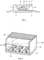
- FIG. 1 shows the construction of an RGB-based white light conversion LED as known per se.
- the light source is a semiconductor device comprising a blue-emitting InGaN chip 1 with a peak emission wavelength of 435 to 455 nm peak wavelength, for example 445 nm, embedded in an opaque base housing 8 in the region of a recess 9.
- the chip 1 is connected via a bonding wire 14 to a first terminal 3 and directly to a second electrical terminal 2.
- the recess 9 is filled with a potting compound 5 containing as main components a silicone (60- 90 wt .-%) and phosphors 6 (about 15 to 40 wt .-%).
- a first phosphor is a green emitting nitrido-orthosilicate phosphor EA 2-xa SE x Eu a Si 1 -y O 4-x-2y N x where EA is Ba and Y is Y.
- the second phosphor used is a red-emitting phosphor, for example an aluminonitridosilicate or calsine.
- the recess has a wall 17, which serves as a reflector for the primary and secondary radiation from the chip 1 and the phosphors 6.
- FIG. 2 shows such a module 20 with various LEDs 24 on a base plate 21.
- a housing is mounted with side walls 22 and a cover plate 12.
- the phosphor mixture is here as a layer 25 on both the side walls and especially on the cover plate 23, the is transparent, attached.
- Suitable light sources are fluorescent lamps or high pressure discharge lamps in which the novel phosphor is used to convert the primary radiation can be alone or in combination with other phosphors.
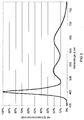
- FIG. 3 shows the spectrum of an LCD backlight LED based on two phosphors.
- the abscissa represents the wavelength in nm, the ordinate the relative emission intensity.
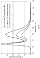
- FIG. 4 shows a comparison of emission spectra of LEDs with incorporated phosphorus concentrations of 9, 13 and 20 wt .-%.
- the abscissa represents the wavelength in nm, the ordinate the relative emission intensity.
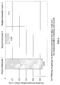
- Embodiment 3 or 4 with a corresponding deficit of SiO 2 demonstrably leads to improved LED stability, especially in humid environments and at higher temperatures.
- FIG. 5 the LED stability is shown at a temperature of 45 ° C and 95% humidity for the four different batch mixes.
- the ordinate is the relative conversion ratio, the abscissa is the time in minutes. It can be seen that Embodiments 3 and 4 are approximately equivalent to each other and both are considerably superior to Comparative Examples 1 and 2.
- the relative quantum efficiencies QE 460 of the novel phosphors according to embodiments 3 and 4 when excited at 460 nm is 3% higher than in comparative example 2.
- Preparation of the represented nitrido-orthosilicates of the form EA 2-xa SE x Eu a Si 1-y O 4 -x -2y N x is typically made of EACO 3 , SiO 2 , SEN and Eu 2 O 3 or EACO 3 , SiO 2 , Si 3 N 4 , (SEN) 2 O 3 and Eu 2 O 3 as starting materials.
- the rare earths are used as (SEN) 2 O 3 , when trivalent oxides are preferably formed.
- rare-earth oxides which are preferably present as mixed oxides, for example Tb is usually present as III / IV mixed oxide Tb 4 O 7 , the mixed oxides are preferably used.
- Y or Sc as nitride or as a combination of oxide and Si 3 N 4 are used.
- fluorides and chlorides such as EACl 2 or SECl 2 , EAF 2 or SECl 2 , but also NH 4 Cl / NH 4 F, H 3 BO 3 , LiF and cryolites, and combinations thereof, can be used as a flux.
- the educts analogous to the batch mixtures 1 to are weighed and homogenized together with a suitable flux. Subsequently, the educt mixture is calcined for several hours under a reducing atmosphere (eg under N 2 or Ar or a mixture of N 2 / H 2 or Ar / H 2 ) at temperatures between 1000 ° C and 1500 ° C. This can be followed by a second annealing, likewise under a reducing atmosphere (for example under N 2 or Ar or a mixture of N 2 / H 2 or Ar / H 2 ) at temperatures between 800 ° C and 1400 ° C.
- a suitable furnace such as a tube or chamber furnace.
- Table 1 below shows a comparison of the spectral properties using the example of a La / N doping with and without an SiO 2 subcutaneous coating.
- Tab. 1 composition ⁇ exc. [Nm] x y ⁇ dom [nm] FWHM [nm] QE [%] (Ba 0.9575 Sr 0.9575 La 0.005 Eu 0.08 ) Si 3.995 N 0.005 460 0285 0638 545.9 64.2 87 (Ba 0.9575 Sr 0.9575 La 0.005 Eu 0.08 ) v 460 0285 0639 545.9 64.1 100
Landscapes
- Chemical & Material Sciences (AREA)
- Inorganic Chemistry (AREA)
- Engineering & Computer Science (AREA)
- Materials Engineering (AREA)
- Organic Chemistry (AREA)
- Luminescent Compositions (AREA)
- Electroluminescent Light Sources (AREA)
- Led Device Packages (AREA)
Applications Claiming Priority (2)
| Application Number | Priority Date | Filing Date | Title |
|---|---|---|---|
| DE102010030473A DE102010030473A1 (de) | 2010-06-24 | 2010-06-24 | Leuchtstoff und Lichtquelle mit derartigem Leuchtstoff |
| PCT/EP2011/059412 WO2011160944A1 (de) | 2010-06-24 | 2011-06-07 | Leuchtstoff und lichtquelle mit derartigem leuchtstoff |
Publications (3)
| Publication Number | Publication Date |
|---|---|
| EP2585554A1 EP2585554A1 (de) | 2013-05-01 |
| EP2585554B1 EP2585554B1 (de) | 2016-08-31 |
| EP2585554B9 true EP2585554B9 (de) | 2017-01-25 |
Family
ID=44357987
Family Applications (1)
| Application Number | Title | Priority Date | Filing Date |
|---|---|---|---|
| EP11727415.9A Active EP2585554B9 (de) | 2010-06-24 | 2011-06-07 | Leuchtstoff und lichtquelle mit derartigem leuchtstoff |
Country Status (7)
| Country | Link |
|---|---|
| US (1) | US20130140981A1 (zh) |
| EP (1) | EP2585554B9 (zh) |
| JP (1) | JP2013536264A (zh) |
| KR (1) | KR20130038340A (zh) |
| CN (1) | CN103097491B (zh) |
| DE (1) | DE102010030473A1 (zh) |
| WO (1) | WO2011160944A1 (zh) |
Families Citing this family (18)
| Publication number | Priority date | Publication date | Assignee | Title |
|---|---|---|---|---|
| DE202011106052U1 (de) | 2011-09-23 | 2011-11-09 | Osram Ag | Lichtquelle mit Leuchtstoff und zugehörige Beleuchtungseinheit. |
| DE102013205329A1 (de) * | 2013-03-26 | 2014-10-16 | Siemens Aktiengesellschaft | Verfahren zum Herstellen einer Leuchtstoffkeramik |
| CN104109536B (zh) * | 2013-04-19 | 2016-03-02 | 四川新力光源股份有限公司 | 氮氧化物发光材料、制备方法及由其制成的led光源 |
| DE102013207448A1 (de) * | 2013-04-24 | 2014-10-30 | Osram Opto Semiconductors Gmbh | Konverterelement, Baugruppe, Hintergrundbeleuchtung und Anzeigevorrichtung |
| DE102013217055B4 (de) * | 2013-05-17 | 2022-08-25 | Tridonic Gmbh & Co Kg | Weisslicht-LED-Modul zur Objektbeleuchtung |
| CN105637063B (zh) | 2013-10-08 | 2018-06-12 | 欧司朗光电半导体有限公司 | 发光材料、用于制造发光材料的方法和发光材料的应用 |
| EP3172168A1 (en) | 2014-07-23 | 2017-05-31 | Solvay SA | Process for manufacture of purified alkaline earth metal carbonate |
| DE102016109138A1 (de) | 2016-05-18 | 2017-11-23 | Osram Gmbh | Optoelektronisches Bauelement und Verwendung eines optoelektronischen Bauelements |
| DE102016121694A1 (de) * | 2016-08-12 | 2018-02-15 | Osram Gmbh | Beleuchtungsvorrichtung |
| DE102016121692A1 (de) | 2016-08-12 | 2018-02-15 | Osram Gmbh | Leuchtstoff und Verfahren zur Herstellung eines Leuchtstoffs |
| CN109642155B (zh) | 2016-08-12 | 2023-04-07 | 欧司朗光电半导体有限公司 | 照明设备 |
| US10644206B2 (en) | 2016-08-12 | 2020-05-05 | Osram Oled Gmbh | Lighting device |
| US10711192B2 (en) | 2016-08-12 | 2020-07-14 | Osram Oled Gmbh | Lighting device |
| JP7050774B2 (ja) | 2016-11-11 | 2022-04-08 | オスラム オプト セミコンダクターズ ゲゼルシャフト ミット ベシュレンクテル ハフツング | 蛍光体、照明装置および照明装置の使用 |
| DE112017005672A5 (de) | 2016-11-11 | 2019-12-24 | Osram Opto Semiconductors Gmbh | Leuchtstoff, beleuchtungsvorrichtung und verwendung einer beleuchtungsvorrichtung |
| CN107011895B (zh) * | 2017-05-26 | 2019-04-09 | 厦门科煜光电有限公司 | 一种蓝绿色led发光材料的制备方法 |
| DE112018004067A5 (de) | 2017-08-10 | 2020-04-23 | Osram Oled Gmbh | Dimmbare Lichtquelle |
| DE102018205464A1 (de) | 2017-11-10 | 2019-05-16 | Osram Opto Semiconductors Gmbh | Beleuchtungsvorrichtung und verwendung einer beleuchtungsvorrichtung |
Family Cites Families (9)
| Publication number | Priority date | Publication date | Assignee | Title |
|---|---|---|---|---|
| NL8900364A (nl) * | 1989-02-15 | 1990-09-03 | Philips Nv | Luminescerend aardalkalimetaal-orthosilicaat, luminescerend scherm voorzien van een dergelijk silicaat en lagedrukkwikdampontladingslamp voorzien van een dergelijk scherm. |
| AT410266B (de) * | 2000-12-28 | 2003-03-25 | Tridonic Optoelectronics Gmbh | Lichtquelle mit einem lichtemittierenden element |
| JP4511849B2 (ja) * | 2004-02-27 | 2010-07-28 | Dowaエレクトロニクス株式会社 | 蛍光体およびその製造方法、光源、並びにled |
| JP4836429B2 (ja) * | 2004-10-18 | 2011-12-14 | 株式会社東芝 | 蛍光体およびこれを用いた発光装置 |
| US7489073B2 (en) * | 2005-04-15 | 2009-02-10 | Patent-Treuhand-Gesellschaft für elektrische Glühlampen mbH | Blue to yellow-orange emitting phosphor, and light source having such a phosphor |
| US7501753B2 (en) * | 2005-08-31 | 2009-03-10 | Lumination Llc | Phosphor and blends thereof for use in LEDs |
| KR100939936B1 (ko) * | 2006-06-21 | 2010-02-04 | 대주전자재료 주식회사 | 툴리움을 포함하는 백색 발광다이오드용 형광체 및 그제조방법 |
| DE102007016228A1 (de) * | 2007-04-04 | 2008-10-09 | Litec Lll Gmbh | Verfahren zur Herstellung von Leuchtstoffen basierend auf Orthosilikaten für pcLEDs |
| CN101591535B (zh) * | 2009-06-29 | 2012-09-19 | 彩虹集团公司 | 一种稀土元素激活的碱土硅酸盐荧光粉的制备方法 |
-
2010
- 2010-06-24 DE DE102010030473A patent/DE102010030473A1/de not_active Withdrawn
-
2011
- 2011-06-07 WO PCT/EP2011/059412 patent/WO2011160944A1/de active Application Filing
- 2011-06-07 KR KR1020137001803A patent/KR20130038340A/ko not_active Application Discontinuation
- 2011-06-07 US US13/805,754 patent/US20130140981A1/en not_active Abandoned
- 2011-06-07 CN CN201180031311.9A patent/CN103097491B/zh active Active
- 2011-06-07 JP JP2013515808A patent/JP2013536264A/ja active Pending
- 2011-06-07 EP EP11727415.9A patent/EP2585554B9/de active Active
Also Published As
| Publication number | Publication date |
|---|---|
| EP2585554A1 (de) | 2013-05-01 |
| CN103097491A (zh) | 2013-05-08 |
| EP2585554B1 (de) | 2016-08-31 |
| US20130140981A1 (en) | 2013-06-06 |
| CN103097491B (zh) | 2014-12-10 |
| JP2013536264A (ja) | 2013-09-19 |
| WO2011160944A1 (de) | 2011-12-29 |
| DE102010030473A1 (de) | 2011-12-29 |
| KR20130038340A (ko) | 2013-04-17 |
Similar Documents
| Publication | Publication Date | Title |
|---|---|---|
| EP2585554B9 (de) | Leuchtstoff und lichtquelle mit derartigem leuchtstoff | |
| DE102007035592B4 (de) | Temperaturstabiler Leuchtstoff, Verwendung eines Leuchtstoffs und Verfahren zur Herstellung eines Leuchtstoffs | |
| DE60307415T2 (de) | Fotolumineszierende stoffe für leuchtdioden, und leuchtdiode | |
| DE112007001638B4 (de) | Leuchtstoff aus der Klasse der Nitridosilikate, Verfahren zur Herstellung eines Leuchtstoff aus der Klasse der Nitridosilikate und Verwendung eines derartigen Leuchtstoffs in einer Lichtquelle | |
| EP1664239B1 (de) | Weiss emittierende led mit definierter farbtemperatur | |
| DE102006016548B9 (de) | Blau bis Gelb-Orange emittierender Leuchtstoff und Lichtquelle mit derartigem Leuchtstoff | |
| EP2718396B9 (de) | Beleuchtungseinheit | |
| EP1966345B1 (de) | Rot emittierender leuchtstoff und lichtquelle mit einem derartigen leuchtstoff | |
| WO2006081803A1 (de) | Gelb emittierender leuchtstoff und lichtquelle mit derartigem leuchtstoff | |
| DE112006003161T5 (de) | Ladungskompensierte Nitridphosphore zur Verwendung in Beleuchtungsanwendungen | |
| DE112011103143B4 (de) | Sialon-leuchtstoff, verfahren zum herstellen desselben und licht-emittierende vorrichtung, welche denselben verwendet | |
| EP1670876B1 (de) | Hocheffizienter leuchtstoff | |
| EP2356196A1 (de) | Rot emittierender sr2s15n8 leuchtstoff und lichtquelle mit derartigem leuchtstoff sowie verfahrer zur herstellung des leuchtstoff | |
| EP2217678B1 (de) | Leuchtstoff und beleuchtungssystem mit derartigem leuchtstoff | |
| EP2220191B1 (de) | Wellenlängenkonvertierte LED | |
| EP2491095B1 (de) | Leuchtstoff und lichtquelle mit derartigem leuchtstoff | |
| CN112852415B (zh) | 一种高色纯度、高稳定性的发光绿色荧光粉及其制备方法 | |
| DE112009001977T5 (de) | Verfahren zur Herstellung eines ß-SiAION-Leuchtstoffs |
Legal Events
| Date | Code | Title | Description |
|---|---|---|---|
| PUAI | Public reference made under article 153(3) epc to a published international application that has entered the european phase |
Free format text: ORIGINAL CODE: 0009012 |
|
| 17P | Request for examination filed |
Effective date: 20130124 |
|
| AK | Designated contracting states |
Kind code of ref document: A1 Designated state(s): AL AT BE BG CH CY CZ DE DK EE ES FI FR GB GR HR HU IE IS IT LI LT LU LV MC MK MT NL NO PL PT RO RS SE SI SK SM TR |
|
| DAX | Request for extension of the european patent (deleted) | ||
| 17Q | First examination report despatched |
Effective date: 20140324 |
|
| RIC1 | Information provided on ipc code assigned before grant |
Ipc: H01J 1/63 20060101ALI20160223BHEP Ipc: H05B 33/12 20060101ALI20160223BHEP Ipc: C09K 11/08 20060101ALI20160223BHEP Ipc: H01L 33/50 20100101ALI20160223BHEP Ipc: C09K 11/77 20060101AFI20160223BHEP Ipc: H05B 33/14 20060101ALI20160223BHEP |
|
| GRAP | Despatch of communication of intention to grant a patent |
Free format text: ORIGINAL CODE: EPIDOSNIGR1 |
|
| INTG | Intention to grant announced |
Effective date: 20160411 |
|
| GRAS | Grant fee paid |
Free format text: ORIGINAL CODE: EPIDOSNIGR3 |
|
| GRAA | (expected) grant |
Free format text: ORIGINAL CODE: 0009210 |
|
| AK | Designated contracting states |
Kind code of ref document: B1 Designated state(s): AL AT BE BG CH CY CZ DE DK EE ES FI FR GB GR HR HU IE IS IT LI LT LU LV MC MK MT NL NO PL PT RO RS SE SI SK SM TR |
|
| REG | Reference to a national code |
Ref country code: CH Ref legal event code: EP Ref country code: GB Ref legal event code: FG4D Free format text: NOT ENGLISH |
|
| REG | Reference to a national code |
Ref country code: IE Ref legal event code: FG4D Free format text: LANGUAGE OF EP DOCUMENT: GERMAN |
|
| REG | Reference to a national code |
Ref country code: DE Ref legal event code: R096 Ref document number: 502011010573 Country of ref document: DE |
|
| REG | Reference to a national code |
Ref country code: AT Ref legal event code: REF Ref document number: 824986 Country of ref document: AT Kind code of ref document: T Effective date: 20161015 |
|
| GRAT | Correction requested after decision to grant or after decision to maintain patent in amended form |
Free format text: ORIGINAL CODE: EPIDOSNCDEC |
|
| REG | Reference to a national code |
Ref country code: NL Ref legal event code: FP |
|
| REG | Reference to a national code |
Ref country code: LT Ref legal event code: MG4D |
|
| PG25 | Lapsed in a contracting state [announced via postgrant information from national office to epo] |
Ref country code: HR Free format text: LAPSE BECAUSE OF FAILURE TO SUBMIT A TRANSLATION OF THE DESCRIPTION OR TO PAY THE FEE WITHIN THE PRESCRIBED TIME-LIMIT Effective date: 20160831 Ref country code: RS Free format text: LAPSE BECAUSE OF FAILURE TO SUBMIT A TRANSLATION OF THE DESCRIPTION OR TO PAY THE FEE WITHIN THE PRESCRIBED TIME-LIMIT Effective date: 20160831 Ref country code: NO Free format text: LAPSE BECAUSE OF FAILURE TO SUBMIT A TRANSLATION OF THE DESCRIPTION OR TO PAY THE FEE WITHIN THE PRESCRIBED TIME-LIMIT Effective date: 20161130 Ref country code: LT Free format text: LAPSE BECAUSE OF FAILURE TO SUBMIT A TRANSLATION OF THE DESCRIPTION OR TO PAY THE FEE WITHIN THE PRESCRIBED TIME-LIMIT Effective date: 20160831 Ref country code: FI Free format text: LAPSE BECAUSE OF FAILURE TO SUBMIT A TRANSLATION OF THE DESCRIPTION OR TO PAY THE FEE WITHIN THE PRESCRIBED TIME-LIMIT Effective date: 20160831 |
|
| PG25 | Lapsed in a contracting state [announced via postgrant information from national office to epo] |
Ref country code: ES Free format text: LAPSE BECAUSE OF FAILURE TO SUBMIT A TRANSLATION OF THE DESCRIPTION OR TO PAY THE FEE WITHIN THE PRESCRIBED TIME-LIMIT Effective date: 20160831 Ref country code: SE Free format text: LAPSE BECAUSE OF FAILURE TO SUBMIT A TRANSLATION OF THE DESCRIPTION OR TO PAY THE FEE WITHIN THE PRESCRIBED TIME-LIMIT Effective date: 20160831 Ref country code: LV Free format text: LAPSE BECAUSE OF FAILURE TO SUBMIT A TRANSLATION OF THE DESCRIPTION OR TO PAY THE FEE WITHIN THE PRESCRIBED TIME-LIMIT Effective date: 20160831 Ref country code: GR Free format text: LAPSE BECAUSE OF FAILURE TO SUBMIT A TRANSLATION OF THE DESCRIPTION OR TO PAY THE FEE WITHIN THE PRESCRIBED TIME-LIMIT Effective date: 20161201 |
|
| PG25 | Lapsed in a contracting state [announced via postgrant information from national office to epo] |
Ref country code: EE Free format text: LAPSE BECAUSE OF FAILURE TO SUBMIT A TRANSLATION OF THE DESCRIPTION OR TO PAY THE FEE WITHIN THE PRESCRIBED TIME-LIMIT Effective date: 20160831 Ref country code: RO Free format text: LAPSE BECAUSE OF FAILURE TO SUBMIT A TRANSLATION OF THE DESCRIPTION OR TO PAY THE FEE WITHIN THE PRESCRIBED TIME-LIMIT Effective date: 20160831 |
|
| PG25 | Lapsed in a contracting state [announced via postgrant information from national office to epo] |
Ref country code: PL Free format text: LAPSE BECAUSE OF FAILURE TO SUBMIT A TRANSLATION OF THE DESCRIPTION OR TO PAY THE FEE WITHIN THE PRESCRIBED TIME-LIMIT Effective date: 20160831 Ref country code: DK Free format text: LAPSE BECAUSE OF FAILURE TO SUBMIT A TRANSLATION OF THE DESCRIPTION OR TO PAY THE FEE WITHIN THE PRESCRIBED TIME-LIMIT Effective date: 20160831 Ref country code: SK Free format text: LAPSE BECAUSE OF FAILURE TO SUBMIT A TRANSLATION OF THE DESCRIPTION OR TO PAY THE FEE WITHIN THE PRESCRIBED TIME-LIMIT Effective date: 20160831 Ref country code: CZ Free format text: LAPSE BECAUSE OF FAILURE TO SUBMIT A TRANSLATION OF THE DESCRIPTION OR TO PAY THE FEE WITHIN THE PRESCRIBED TIME-LIMIT Effective date: 20160831 Ref country code: BG Free format text: LAPSE BECAUSE OF FAILURE TO SUBMIT A TRANSLATION OF THE DESCRIPTION OR TO PAY THE FEE WITHIN THE PRESCRIBED TIME-LIMIT Effective date: 20161130 Ref country code: SM Free format text: LAPSE BECAUSE OF FAILURE TO SUBMIT A TRANSLATION OF THE DESCRIPTION OR TO PAY THE FEE WITHIN THE PRESCRIBED TIME-LIMIT Effective date: 20160831 Ref country code: PT Free format text: LAPSE BECAUSE OF FAILURE TO SUBMIT A TRANSLATION OF THE DESCRIPTION OR TO PAY THE FEE WITHIN THE PRESCRIBED TIME-LIMIT Effective date: 20170102 |
|
| REG | Reference to a national code |
Ref country code: DE Ref legal event code: R097 Ref document number: 502011010573 Country of ref document: DE |
|
| PLBE | No opposition filed within time limit |
Free format text: ORIGINAL CODE: 0009261 |
|
| STAA | Information on the status of an ep patent application or granted ep patent |
Free format text: STATUS: NO OPPOSITION FILED WITHIN TIME LIMIT |
|
| 26N | No opposition filed |
Effective date: 20170601 |
|
| PG25 | Lapsed in a contracting state [announced via postgrant information from national office to epo] |
Ref country code: SI Free format text: LAPSE BECAUSE OF FAILURE TO SUBMIT A TRANSLATION OF THE DESCRIPTION OR TO PAY THE FEE WITHIN THE PRESCRIBED TIME-LIMIT Effective date: 20160831 |
|
| PG25 | Lapsed in a contracting state [announced via postgrant information from national office to epo] |
Ref country code: MC Free format text: LAPSE BECAUSE OF FAILURE TO SUBMIT A TRANSLATION OF THE DESCRIPTION OR TO PAY THE FEE WITHIN THE PRESCRIBED TIME-LIMIT Effective date: 20160831 |
|
| REG | Reference to a national code |
Ref country code: CH Ref legal event code: PL |
|
| GBPC | Gb: european patent ceased through non-payment of renewal fee |
Effective date: 20170607 |
|
| REG | Reference to a national code |
Ref country code: IE Ref legal event code: MM4A |
|
| REG | Reference to a national code |
Ref country code: FR Ref legal event code: ST Effective date: 20180228 |
|
| PG25 | Lapsed in a contracting state [announced via postgrant information from national office to epo] |
Ref country code: LI Free format text: LAPSE BECAUSE OF NON-PAYMENT OF DUE FEES Effective date: 20170630 Ref country code: LU Free format text: LAPSE BECAUSE OF NON-PAYMENT OF DUE FEES Effective date: 20170607 Ref country code: CH Free format text: LAPSE BECAUSE OF NON-PAYMENT OF DUE FEES Effective date: 20170630 Ref country code: IE Free format text: LAPSE BECAUSE OF NON-PAYMENT OF DUE FEES Effective date: 20170607 Ref country code: GB Free format text: LAPSE BECAUSE OF NON-PAYMENT OF DUE FEES Effective date: 20170607 |
|
| PG25 | Lapsed in a contracting state [announced via postgrant information from national office to epo] |
Ref country code: FR Free format text: LAPSE BECAUSE OF NON-PAYMENT OF DUE FEES Effective date: 20170630 |
|
| REG | Reference to a national code |
Ref country code: BE Ref legal event code: MM Effective date: 20170630 |
|
| PG25 | Lapsed in a contracting state [announced via postgrant information from national office to epo] |
Ref country code: BE Free format text: LAPSE BECAUSE OF NON-PAYMENT OF DUE FEES Effective date: 20170630 |
|
| PG25 | Lapsed in a contracting state [announced via postgrant information from national office to epo] |
Ref country code: MT Free format text: LAPSE BECAUSE OF FAILURE TO SUBMIT A TRANSLATION OF THE DESCRIPTION OR TO PAY THE FEE WITHIN THE PRESCRIBED TIME-LIMIT Effective date: 20160831 |
|
| PG25 | Lapsed in a contracting state [announced via postgrant information from national office to epo] |
Ref country code: AL Free format text: LAPSE BECAUSE OF FAILURE TO SUBMIT A TRANSLATION OF THE DESCRIPTION OR TO PAY THE FEE WITHIN THE PRESCRIBED TIME-LIMIT Effective date: 20160831 |
|
| PG25 | Lapsed in a contracting state [announced via postgrant information from national office to epo] |
Ref country code: HU Free format text: LAPSE BECAUSE OF FAILURE TO SUBMIT A TRANSLATION OF THE DESCRIPTION OR TO PAY THE FEE WITHIN THE PRESCRIBED TIME-LIMIT; INVALID AB INITIO Effective date: 20110607 |
|
| PG25 | Lapsed in a contracting state [announced via postgrant information from national office to epo] |
Ref country code: CY Free format text: LAPSE BECAUSE OF NON-PAYMENT OF DUE FEES Effective date: 20160831 |
|
| PG25 | Lapsed in a contracting state [announced via postgrant information from national office to epo] |
Ref country code: MK Free format text: LAPSE BECAUSE OF FAILURE TO SUBMIT A TRANSLATION OF THE DESCRIPTION OR TO PAY THE FEE WITHIN THE PRESCRIBED TIME-LIMIT Effective date: 20160831 |
|
| PG25 | Lapsed in a contracting state [announced via postgrant information from national office to epo] |
Ref country code: TR Free format text: LAPSE BECAUSE OF FAILURE TO SUBMIT A TRANSLATION OF THE DESCRIPTION OR TO PAY THE FEE WITHIN THE PRESCRIBED TIME-LIMIT Effective date: 20160831 |
|
| PG25 | Lapsed in a contracting state [announced via postgrant information from national office to epo] |
Ref country code: IS Free format text: LAPSE BECAUSE OF FAILURE TO SUBMIT A TRANSLATION OF THE DESCRIPTION OR TO PAY THE FEE WITHIN THE PRESCRIBED TIME-LIMIT Effective date: 20161231 |
|
| PGFP | Annual fee paid to national office [announced via postgrant information from national office to epo] |
Ref country code: NL Payment date: 20230620 Year of fee payment: 13 Ref country code: DE Payment date: 20230620 Year of fee payment: 13 |
|
| PGFP | Annual fee paid to national office [announced via postgrant information from national office to epo] |
Ref country code: AT Payment date: 20230621 Year of fee payment: 13 |
|
| P01 | Opt-out of the competence of the unified patent court (upc) registered |
Effective date: 20230821 |
|
| PGFP | Annual fee paid to national office [announced via postgrant information from national office to epo] |
Ref country code: IT Payment date: 20230623 Year of fee payment: 13 |