EP2581953B1 - Dispositif électroluminescent - Google Patents
Dispositif électroluminescent Download PDFInfo
- Publication number
- EP2581953B1 EP2581953B1 EP12155005.7A EP12155005A EP2581953B1 EP 2581953 B1 EP2581953 B1 EP 2581953B1 EP 12155005 A EP12155005 A EP 12155005A EP 2581953 B1 EP2581953 B1 EP 2581953B1
- Authority
- EP
- European Patent Office
- Prior art keywords
- electrode
- light emitting
- layer
- emitting device
- semiconductor layer
- Prior art date
- Legal status (The legal status is an assumption and is not a legal conclusion. Google has not performed a legal analysis and makes no representation as to the accuracy of the status listed.)
- Active
Links
- 239000004065 semiconductor Substances 0.000 claims description 130
- 239000000758 substrate Substances 0.000 claims description 22
- 125000006850 spacer group Chemical group 0.000 claims description 6
- 230000004888 barrier function Effects 0.000 claims description 5
- -1 acryl Chemical group 0.000 claims description 4
- JOYRKODLDBILNP-UHFFFAOYSA-N Ethyl urethane Chemical compound CCOC(N)=O JOYRKODLDBILNP-UHFFFAOYSA-N 0.000 claims description 3
- 239000011368 organic material Substances 0.000 claims description 3
- 229920000728 polyester Polymers 0.000 claims description 3
- 239000010410 layer Substances 0.000 description 262
- 239000003566 sealing material Substances 0.000 description 26
- 239000000126 substance Substances 0.000 description 24
- 239000004973 liquid crystal related substance Substances 0.000 description 18
- 239000000463 material Substances 0.000 description 15
- VYPSYNLAJGMNEJ-UHFFFAOYSA-N Silicium dioxide Chemical compound O=[Si]=O VYPSYNLAJGMNEJ-UHFFFAOYSA-N 0.000 description 10
- 239000010408 film Substances 0.000 description 10
- 238000000605 extraction Methods 0.000 description 9
- 230000001965 increasing effect Effects 0.000 description 9
- 230000006866 deterioration Effects 0.000 description 8
- 239000000203 mixture Substances 0.000 description 7
- 230000005855 radiation Effects 0.000 description 7
- 239000004020 conductor Substances 0.000 description 6
- RKTYLMNFRDHKIL-UHFFFAOYSA-N copper;5,10,15,20-tetraphenylporphyrin-22,24-diide Chemical compound [Cu+2].C1=CC(C(=C2C=CC([N-]2)=C(C=2C=CC=CC=2)C=2C=CC(N=2)=C(C=2C=CC=CC=2)C2=CC=C3[N-]2)C=2C=CC=CC=2)=NC1=C3C1=CC=CC=C1 RKTYLMNFRDHKIL-UHFFFAOYSA-N 0.000 description 6
- 238000009877 rendering Methods 0.000 description 6
- 239000010409 thin film Substances 0.000 description 6
- 229910002704 AlGaN Inorganic materials 0.000 description 5
- 230000003247 decreasing effect Effects 0.000 description 5
- 229910052751 metal Inorganic materials 0.000 description 5
- 239000002184 metal Substances 0.000 description 5
- 239000000377 silicon dioxide Substances 0.000 description 5
- GWEVSGVZZGPLCZ-UHFFFAOYSA-N Titan oxide Chemical compound O=[Ti]=O GWEVSGVZZGPLCZ-UHFFFAOYSA-N 0.000 description 4
- 239000002019 doping agent Substances 0.000 description 4
- 230000005284 excitation Effects 0.000 description 4
- 230000001788 irregular Effects 0.000 description 4
- CPLXHLVBOLITMK-UHFFFAOYSA-N magnesium oxide Inorganic materials [Mg]=O CPLXHLVBOLITMK-UHFFFAOYSA-N 0.000 description 4
- 239000000395 magnesium oxide Substances 0.000 description 4
- AXZKOIWUVFPNLO-UHFFFAOYSA-N magnesium;oxygen(2-) Chemical compound [O-2].[Mg+2] AXZKOIWUVFPNLO-UHFFFAOYSA-N 0.000 description 4
- 238000000034 method Methods 0.000 description 4
- SIWVEOZUMHYXCS-UHFFFAOYSA-N oxo(oxoyttriooxy)yttrium Chemical compound O=[Y]O[Y]=O SIWVEOZUMHYXCS-UHFFFAOYSA-N 0.000 description 4
- 238000005229 chemical vapour deposition Methods 0.000 description 3
- 239000000470 constituent Substances 0.000 description 3
- 230000002708 enhancing effect Effects 0.000 description 3
- VRIVJOXICYMTAG-IYEMJOQQSA-L iron(ii) gluconate Chemical compound [Fe+2].OC[C@@H](O)[C@@H](O)[C@H](O)[C@@H](O)C([O-])=O.OC[C@@H](O)[C@@H](O)[C@H](O)[C@@H](O)C([O-])=O VRIVJOXICYMTAG-IYEMJOQQSA-L 0.000 description 3
- 239000012788 optical film Substances 0.000 description 3
- 229910052710 silicon Inorganic materials 0.000 description 3
- 239000002356 single layer Substances 0.000 description 3
- 229910000679 solder Inorganic materials 0.000 description 3
- 229910016287 MxOy Inorganic materials 0.000 description 2
- 229910019897 RuOx Inorganic materials 0.000 description 2
- 229910052782 aluminium Inorganic materials 0.000 description 2
- QVQLCTNNEUAWMS-UHFFFAOYSA-N barium oxide Chemical compound [Ba]=O QVQLCTNNEUAWMS-UHFFFAOYSA-N 0.000 description 2
- 230000008859 change Effects 0.000 description 2
- 150000001875 compounds Chemical class 0.000 description 2
- 238000001312 dry etching Methods 0.000 description 2
- 238000005530 etching Methods 0.000 description 2
- 229910052732 germanium Inorganic materials 0.000 description 2
- 229910052737 gold Inorganic materials 0.000 description 2
- 238000002248 hydride vapour-phase epitaxy Methods 0.000 description 2
- 229910010272 inorganic material Inorganic materials 0.000 description 2
- 239000011147 inorganic material Substances 0.000 description 2
- 230000031700 light absorption Effects 0.000 description 2
- 239000007788 liquid Substances 0.000 description 2
- 229910052749 magnesium Inorganic materials 0.000 description 2
- 239000011777 magnesium Substances 0.000 description 2
- 238000004519 manufacturing process Methods 0.000 description 2
- 239000007769 metal material Substances 0.000 description 2
- 238000000465 moulding Methods 0.000 description 2
- 229910052759 nickel Inorganic materials 0.000 description 2
- 150000004767 nitrides Chemical class 0.000 description 2
- TWNQGVIAIRXVLR-UHFFFAOYSA-N oxo(oxoalumanyloxy)alumane Chemical compound O=[Al]O[Al]=O TWNQGVIAIRXVLR-UHFFFAOYSA-N 0.000 description 2
- 238000000623 plasma-assisted chemical vapour deposition Methods 0.000 description 2
- 229920003229 poly(methyl methacrylate) Polymers 0.000 description 2
- 229920000139 polyethylene terephthalate Polymers 0.000 description 2
- 239000005020 polyethylene terephthalate Substances 0.000 description 2
- 239000004926 polymethyl methacrylate Substances 0.000 description 2
- 230000008569 process Effects 0.000 description 2
- 230000001681 protective effect Effects 0.000 description 2
- 235000012239 silicon dioxide Nutrition 0.000 description 2
- 229910052709 silver Inorganic materials 0.000 description 2
- 238000001039 wet etching Methods 0.000 description 2
- 229910052725 zinc Inorganic materials 0.000 description 2
- 229910018229 Al—Ga Inorganic materials 0.000 description 1
- BTBUEUYNUDRHOZ-UHFFFAOYSA-N Borate Chemical compound [O-]B([O-])[O-] BTBUEUYNUDRHOZ-UHFFFAOYSA-N 0.000 description 1
- 239000004593 Epoxy Substances 0.000 description 1
- KRHYYFGTRYWZRS-UHFFFAOYSA-M Fluoride anion Chemical compound [F-] KRHYYFGTRYWZRS-UHFFFAOYSA-M 0.000 description 1
- 108010043121 Green Fluorescent Proteins Proteins 0.000 description 1
- BPQQTUXANYXVAA-UHFFFAOYSA-N Orthosilicate Chemical compound [O-][Si]([O-])([O-])[O-] BPQQTUXANYXVAA-UHFFFAOYSA-N 0.000 description 1
- 229910019142 PO4 Inorganic materials 0.000 description 1
- XUIMIQQOPSSXEZ-UHFFFAOYSA-N Silicon Chemical compound [Si] XUIMIQQOPSSXEZ-UHFFFAOYSA-N 0.000 description 1
- BQCADISMDOOEFD-UHFFFAOYSA-N Silver Chemical compound [Ag] BQCADISMDOOEFD-UHFFFAOYSA-N 0.000 description 1
- UCKMPCXJQFINFW-UHFFFAOYSA-N Sulphide Chemical compound [S-2] UCKMPCXJQFINFW-UHFFFAOYSA-N 0.000 description 1
- 229910008842 WTi Inorganic materials 0.000 description 1
- 229910001361 White metal Inorganic materials 0.000 description 1
- 229910045601 alloy Inorganic materials 0.000 description 1
- 239000000956 alloy Substances 0.000 description 1
- 150000004645 aluminates Chemical class 0.000 description 1
- XAGFODPZIPBFFR-UHFFFAOYSA-N aluminium Chemical compound [Al] XAGFODPZIPBFFR-UHFFFAOYSA-N 0.000 description 1
- 229910052788 barium Inorganic materials 0.000 description 1
- 230000000903 blocking effect Effects 0.000 description 1
- 229910052791 calcium Inorganic materials 0.000 description 1
- 239000000919 ceramic Substances 0.000 description 1
- 229910052804 chromium Inorganic materials 0.000 description 1
- 239000003086 colorant Substances 0.000 description 1
- 239000012141 concentrate Substances 0.000 description 1
- 238000010276 construction Methods 0.000 description 1
- 229910052802 copper Inorganic materials 0.000 description 1
- 238000002425 crystallisation Methods 0.000 description 1
- 230000008025 crystallization Effects 0.000 description 1
- 238000009792 diffusion process Methods 0.000 description 1
- 238000009826 distribution Methods 0.000 description 1
- 230000005611 electricity Effects 0.000 description 1
- 238000011049 filling Methods 0.000 description 1
- 230000004313 glare Effects 0.000 description 1
- 239000011521 glass Substances 0.000 description 1
- 229910052735 hafnium Inorganic materials 0.000 description 1
- 229910052738 indium Inorganic materials 0.000 description 1
- 238000003780 insertion Methods 0.000 description 1
- 230000037431 insertion Effects 0.000 description 1
- 229910052741 iridium Inorganic materials 0.000 description 1
- 150000004706 metal oxides Chemical class 0.000 description 1
- 238000012986 modification Methods 0.000 description 1
- 230000004048 modification Effects 0.000 description 1
- 238000001451 molecular beam epitaxy Methods 0.000 description 1
- 229910052750 molybdenum Inorganic materials 0.000 description 1
- 229910052758 niobium Inorganic materials 0.000 description 1
- 230000010355 oscillation Effects 0.000 description 1
- 238000012858 packaging process Methods 0.000 description 1
- 229910052763 palladium Inorganic materials 0.000 description 1
- 239000002245 particle Substances 0.000 description 1
- NBIIXXVUZAFLBC-UHFFFAOYSA-K phosphate Chemical compound [O-]P([O-])([O-])=O NBIIXXVUZAFLBC-UHFFFAOYSA-K 0.000 description 1
- 239000010452 phosphate Substances 0.000 description 1
- 239000004033 plastic Substances 0.000 description 1
- 229920003023 plastic Polymers 0.000 description 1
- 229910052697 platinum Inorganic materials 0.000 description 1
- 229920000515 polycarbonate Polymers 0.000 description 1
- 239000004417 polycarbonate Substances 0.000 description 1
- 239000002096 quantum dot Substances 0.000 description 1
- 230000000191 radiation effect Effects 0.000 description 1
- 230000006798 recombination Effects 0.000 description 1
- 238000005215 recombination Methods 0.000 description 1
- 230000009467 reduction Effects 0.000 description 1
- 239000011347 resin Substances 0.000 description 1
- 229920005989 resin Polymers 0.000 description 1
- 230000004044 response Effects 0.000 description 1
- 229910052702 rhenium Inorganic materials 0.000 description 1
- 229910052707 ruthenium Inorganic materials 0.000 description 1
- 238000000926 separation method Methods 0.000 description 1
- 239000010703 silicon Substances 0.000 description 1
- 239000002210 silicon-based material Substances 0.000 description 1
- 239000004332 silver Substances 0.000 description 1
- 238000004544 sputter deposition Methods 0.000 description 1
- 229910052712 strontium Inorganic materials 0.000 description 1
- 229920003002 synthetic resin Polymers 0.000 description 1
- 239000000057 synthetic resin Substances 0.000 description 1
- 238000001029 thermal curing Methods 0.000 description 1
- 229910052718 tin Inorganic materials 0.000 description 1
- 239000010936 titanium Substances 0.000 description 1
- 229910052719 titanium Inorganic materials 0.000 description 1
- 239000004408 titanium dioxide Substances 0.000 description 1
- 238000002834 transmittance Methods 0.000 description 1
- 239000012780 transparent material Substances 0.000 description 1
- 229910052721 tungsten Inorganic materials 0.000 description 1
- 239000010969 white metal Substances 0.000 description 1
Images


Classifications
-
- H—ELECTRICITY
- H01—ELECTRIC ELEMENTS
- H01L—SEMICONDUCTOR DEVICES NOT COVERED BY CLASS H10
- H01L33/00—Semiconductor devices with at least one potential-jump barrier or surface barrier specially adapted for light emission; Processes or apparatus specially adapted for the manufacture or treatment thereof or of parts thereof; Details thereof
- H01L33/44—Semiconductor devices with at least one potential-jump barrier or surface barrier specially adapted for light emission; Processes or apparatus specially adapted for the manufacture or treatment thereof or of parts thereof; Details thereof characterised by the coatings, e.g. passivation layer or anti-reflective coating
-
- H—ELECTRICITY
- H01—ELECTRIC ELEMENTS
- H01L—SEMICONDUCTOR DEVICES NOT COVERED BY CLASS H10
- H01L2924/00—Indexing scheme for arrangements or methods for connecting or disconnecting semiconductor or solid-state bodies as covered by H01L24/00
- H01L2924/0001—Technical content checked by a classifier
- H01L2924/0002—Not covered by any one of groups H01L24/00, H01L24/00 and H01L2224/00
-
- H—ELECTRICITY
- H01—ELECTRIC ELEMENTS
- H01L—SEMICONDUCTOR DEVICES NOT COVERED BY CLASS H10
- H01L33/00—Semiconductor devices with at least one potential-jump barrier or surface barrier specially adapted for light emission; Processes or apparatus specially adapted for the manufacture or treatment thereof or of parts thereof; Details thereof
- H01L33/02—Semiconductor devices with at least one potential-jump barrier or surface barrier specially adapted for light emission; Processes or apparatus specially adapted for the manufacture or treatment thereof or of parts thereof; Details thereof characterised by the semiconductor bodies
- H01L33/08—Semiconductor devices with at least one potential-jump barrier or surface barrier specially adapted for light emission; Processes or apparatus specially adapted for the manufacture or treatment thereof or of parts thereof; Details thereof characterised by the semiconductor bodies with a plurality of light emitting regions, e.g. laterally discontinuous light emitting layer or photoluminescent region integrated within the semiconductor body
-
- H—ELECTRICITY
- H01—ELECTRIC ELEMENTS
- H01L—SEMICONDUCTOR DEVICES NOT COVERED BY CLASS H10
- H01L33/00—Semiconductor devices with at least one potential-jump barrier or surface barrier specially adapted for light emission; Processes or apparatus specially adapted for the manufacture or treatment thereof or of parts thereof; Details thereof
- H01L33/02—Semiconductor devices with at least one potential-jump barrier or surface barrier specially adapted for light emission; Processes or apparatus specially adapted for the manufacture or treatment thereof or of parts thereof; Details thereof characterised by the semiconductor bodies
- H01L33/20—Semiconductor devices with at least one potential-jump barrier or surface barrier specially adapted for light emission; Processes or apparatus specially adapted for the manufacture or treatment thereof or of parts thereof; Details thereof characterised by the semiconductor bodies with a particular shape, e.g. curved or truncated substrate
-
- H—ELECTRICITY
- H01—ELECTRIC ELEMENTS
- H01L—SEMICONDUCTOR DEVICES NOT COVERED BY CLASS H10
- H01L33/00—Semiconductor devices with at least one potential-jump barrier or surface barrier specially adapted for light emission; Processes or apparatus specially adapted for the manufacture or treatment thereof or of parts thereof; Details thereof
- H01L33/36—Semiconductor devices with at least one potential-jump barrier or surface barrier specially adapted for light emission; Processes or apparatus specially adapted for the manufacture or treatment thereof or of parts thereof; Details thereof characterised by the electrodes
- H01L33/38—Semiconductor devices with at least one potential-jump barrier or surface barrier specially adapted for light emission; Processes or apparatus specially adapted for the manufacture or treatment thereof or of parts thereof; Details thereof characterised by the electrodes with a particular shape
-
- H—ELECTRICITY
- H01—ELECTRIC ELEMENTS
- H01L—SEMICONDUCTOR DEVICES NOT COVERED BY CLASS H10
- H01L33/00—Semiconductor devices with at least one potential-jump barrier or surface barrier specially adapted for light emission; Processes or apparatus specially adapted for the manufacture or treatment thereof or of parts thereof; Details thereof
- H01L33/44—Semiconductor devices with at least one potential-jump barrier or surface barrier specially adapted for light emission; Processes or apparatus specially adapted for the manufacture or treatment thereof or of parts thereof; Details thereof characterised by the coatings, e.g. passivation layer or anti-reflective coating
- H01L33/46—Reflective coating, e.g. dielectric Bragg reflector
-
- H—ELECTRICITY
- H01—ELECTRIC ELEMENTS
- H01L—SEMICONDUCTOR DEVICES NOT COVERED BY CLASS H10
- H01L33/00—Semiconductor devices with at least one potential-jump barrier or surface barrier specially adapted for light emission; Processes or apparatus specially adapted for the manufacture or treatment thereof or of parts thereof; Details thereof
- H01L33/48—Semiconductor devices with at least one potential-jump barrier or surface barrier specially adapted for light emission; Processes or apparatus specially adapted for the manufacture or treatment thereof or of parts thereof; Details thereof characterised by the semiconductor body packages
- H01L33/50—Wavelength conversion elements
- H01L33/508—Wavelength conversion elements having a non-uniform spatial arrangement or non-uniform concentration, e.g. patterned wavelength conversion layer, wavelength conversion layer with a concentration gradient of the wavelength conversion material
Definitions
- Embodiments relate to a light emitting device, which is of a flip chip type with enhanced light emission efficiency and exhibits stability and reliability upon bonding to a light emitting device package.
- LEDs Light Emitting Diodes
- LEDs are a representative example of light emitting devices, which convert electric signals into infrared light or visible light using characteristics of compound semiconductors. Such LEDs are being utilized in home appliances, remote controllers, electronic bulletin boards, displays and various other automated machines. The application range of LEDs is gradually increasing.
- Exemplary LEDs mounted in flip chip configurations are disclosed in US 2006/0169994 A1 and US 2011/0233588 A1 .
- miniature LEDs are fabricated into surface mount devices so as to be directly mounted on a Printed Circuit Board (PCB) and hence, an LED lamp, which serves as a display device, is being developed into a surface mount device.
- the surface mount device can substitute for a conventional simple lamp and is used in a variety of color on-and-off displays and letter/image displays.
- the increased application range of LEDs causes a demand for higher brightness of household lights as well as emergency lights and therefore, it is important to enhance brightness of LEDs.
- Embodiments provide a light emitting device, which is of a flip chip type with enhanced light emission efficiency and exhibits stability and reliability upon bonding to a light emitting device package.
- a light emitting device is as defined in claim 1. Embodiments are further defined in claims 2-11 There is also provided a light emitting device package as defined in claim 12.
- spatially-relative terms such as “below”, “beneath”, “lower”, “above”, or “upper” may be used herein to describe one element's relationship to another element as illustrated in the Figures. It will be understood that spatially-relative terms are intended to encompass different orientations of the device in addition to the orientation depicted in the Figures. For example, if the device in one of the figures is turned over, elements described as “below” or “beneath” other elements would then be oriented “above” the other elements. The exemplary terms “below” or “beneath” can, therefore, encompass both an orientation of above and below. Since the device may be oriented in another direction, the spatially-relative terms may be interpreted in accordance with the orientation of the device.
- each layer is exaggerated, omitted, or schematically illustrated for convenience of description and clarity. Also, the size or area of each constituent element does not entirely reflect the actual size thereof.
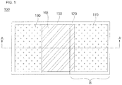
- FIG. 1 is a plan view showing a light emitting device in accordance with an embodiment
- FIG. 2 is a sectional view taken along the line A-A' of the light emitting device shown in FIG. 1 .
- the light emitting device 100 may include a support member 110 and a light emitting structure disposed on the support member 110.
- the light emitting structure may include a first semiconductor layer 120, a second semiconductor layer 140 and an active layer 130 interposed between the first semiconductor layer 120 and the second semiconductor layer 140.
- the support member 110 may be formed of a light transmittable material including, for example, any one of sapphire (Al 2 O 3 ), GaN, ZnO and AlO, although the disclosure is not limited thereto.
- a SiC support member which has a greater thermal conductivity than the sapphire (Al 2 O 3 ) support member, may be used. It is noted that the support member 110 may have an index of refraction less than that of the first semiconductor layer 120, for the sake of light extraction efficiency.
- an uneven surface pattern 112 may be formed at a lower surface of the support member 110.
- the uneven surface pattern 112 may be formed at one surface of the support member 110 opposite to the other surface where the light emitting structure is formed.
- the uneven surface pattern 112 may be formed by etching, more particularly, dry etching or wet etching, although the disclosure is not limited thereto. Such an uneven surface structure serves to prevent total reflection of light to be emitted, which may enhance light extraction efficiency.
- a buffer layer may be disposed on the support member 110, so as to relieve lattice mismatch between the support member 110 and the first semiconductor layer 120 and to enable easy growth of the first semiconductor layer 120.
- the buffer layer may be grown under a low temperature atmosphere and may be formed of a material capable of relieving a difference in a lattice constant between the first semiconductor layer 120 and the support member 110.
- the buffer layer may be formed of any one material selected from among GaN, InN, AIN, AlInN, InGaN, AlGaN and InAlGaN, although the disclosure is not limited thereto.
- the light emitting structure which includes the first semiconductor layer 120, the active layer 130 and the second semiconductor layer 140, may be formed on the buffer layer (not shown).
- the first semiconductor layer 120 may be disposed on the buffer layer (not shown).
- the first semiconductor layer 120 may be an n-type semiconductor layer and may provide the active layer 130 with electrons.
- the first semiconductor layer 120 may be formed of a semiconductor material having a composition of In x Al y Ga 1-x-y N (0 ⁇ x ⁇ 1, 0 ⁇ y ⁇ 1, 0 ⁇ x+y ⁇ 1).
- the first semiconductor layer 120 may be formed of a material selected from among GaN, AlN, AlGaN, InGaN, InN, InAlGaN, AlInN and the like.
- the first semiconductor layer 120 may be doped with an n-type dopant, such as Si, Ge, Sn and the like.
- An undoped semiconductor layer may be further provided beneath the first semiconductor layer 120, although the disclosure is not limited thereto.
- the undoped semiconductor layer (not shown) serves to enhance crystallization of the first semiconductor layer 120.
- the undoped semiconductor layer may be identical to the first semiconductor layer 120, except that it is not doped with an n-type dopant and has lower electric conductivity than the first semiconductor layer 120.
- the active layer 130 may be formed on the first semiconductor layer 120.
- the active layer 130 may be formed of a group III-V compound semiconductor material to have a single or multiple quantum well structure, a quantum wire structure, a quantum dot structure or the like.
- the active layer 130 may have a single or multiple quantum well structure including a well layer having a composition of In x Al y Ga 1 - x-y N (0 ⁇ x ⁇ 1, 0 ⁇ y ⁇ 1, 0 ⁇ x+y ⁇ 1) and a barrier layer having a composition of In a Al b Ga 1-a-b N (0 ⁇ a ⁇ 1, 0 ⁇ b ⁇ 1, 0 ⁇ a+b ⁇ 1).
- the well layer may be formed of a material having a smaller band gap than the barrier layer.
- a conductive clad layer may be formed above and/or below the active layer 130.
- the conductive clad layer may be formed of an AlGaN-based semiconductor and may have a greater band gap than the active layer 130.
- the second semiconductor layer 140 may be a p-type semiconductor layer and may provide the active layer 130 with holes.
- the second semiconductor layer 140 may be formed of a semiconductor material having a composition of In x Al y Ga 1-x-y N (0 ⁇ x ⁇ 1, 0 ⁇ y ⁇ 1, 0 ⁇ x+y ⁇ 1).
- the second semiconductor layer 140 may be formed of a material selected from among GaN, AlN, AlGaN, InGaN, InN, InAlGaN, AlInN and the like.
- the second semiconductor layer 140 may be doped with a p-type dopant, such as Mg, Zn, Ca, Sr, Ba and the like.
- An intermediate layer (not shown) may be formed between the active layer 130 and the second semiconductor layer 140.
- the intermediate layer may be an electron blocking layer, which prevents electrons, injected from the first semiconductor layer 120 into the active layer 130, from moving to the second semiconductor layer 140, rather than being recombined in the active layer 130, when high current is applied.
- the intermediate layer may have a greater band gap than the active layer 130, which may prevent electrons, injected from the first semiconductor layer 120, from being injected into the second semiconductor layer 140, rather than being recombined in the active layer 130. Accordingly, the intermediate layer may enhance electron-hole recombination possibility in the active layer 130 and may prevent current leakage.
- the above described intermediate layer may have a greater band gap than the barrier layer included in the active layer 130 and may be a semiconductor layer containing Al, such as p-type AlGaN, although the disclosure is not limited thereto.
- the first semiconductor layer 120, the active layer 130 and the second semiconductor layer 140 as described above, for example, may be formed using Metal Organic Chemical Vapor Deposition (MOCVD), Chemical Vapor Deposition (CVD), Plasma Enhanced Chemical Vapor Deposition (PECVD), Molecular Beam Epitaxy (MBE), Hydride Vapor Phase Epitaxy (HVPE), sputtering and the like, although the disclosure is not limited thereto.
- MOCVD Metal Organic Chemical Vapor Deposition
- CVD Chemical Vapor Deposition
- PECVD Plasma Enhanced Chemical Vapor Deposition
- MBE Molecular Beam Epitaxy
- HVPE Hydride Vapor Phase Epitaxy
- the conductive dopant contained in first semiconductor layer 120 and the second semiconductor layer 140 may have an even or uneven doping density.
- the plurality of semiconductor layers may be formed within a wide doping density range, although the disclosure is not limited thereto.
- the first semiconductor layer 120 may be a p-type semiconductor layer
- the second semiconductor layer 140 may be an n-type semiconductor layer
- a third semiconductor layer (not shown), which includes an n-type or p-type semiconductor layer, may be formed on the second semiconductor layer 140.
- the light emitting device 100 may have at least one among np, pn, npn and pnp junction structures.
- a light transmittable electrode layer 150 may be disposed on the second semiconductor layer 140.
- a second electrode 180 may be connected to the second semiconductor layer 140 or may be connected to the light transmittable electrode layer 150, although the disclosure is not limited thereto.
- the light transmittable electrode layer 150 may be formed of at least one selected from among ITO, IZO(In-ZnO), GZO(Ga-ZnO), AZO(Al-ZnO), AGZO(Al-Ga ZnO), IGZO(In-Ga ZnO), IrO x , RuO x , RuOx/ITO, Ni/IrO x /Au and Ni/IrO x /Au/ITO.
- the light transmittable electrode layer 150 may be formed over the entire outer surface of the second semiconductor layer 140, so as to prevent current crowding.
- the light emitting device 100 may include a first region B, which exposes a part of an upper surface of the first semiconductor layer 120 to the outside.
- the light emitting device 100 may include a first electrode 170, which is disposed on the first semiconductor layer 120 in the first region B, and a second electrode 180 which is disposed on the second semiconductor layer 140.
- An insulating layer 168 may be disposed at least between the light emitting structure and the first electrode 170.
- the first electrode 170 may be disposed on the exposed part of the upper surface of the first semiconductor layer 120 in the first region B. More particularly, at least a part of the second semiconductor layer 140 and a part of the active layer 130 are removed to expose the first semiconductor layer 120 in the first region B, and the first electrode 170 is disposed on the first semiconductor layer 120 in the first region B.
- the first electrode 170 may be spaced apart from a lateral surface of the second semiconductor layer 140 and a lateral surface of the active layer 130 by a first distance. Additionally, upper and lower surfaces of the first electrode 170 may have different areas.
- an area of an upper surface of the first electrode 170 may be in a range of 40% to 99% an area of the second semiconductor layer 140.
- the area is measured on the basis of the surface when the light emitting device 100 is viewed from the top. This will be equally applied in the following description. If the area of the first electrode 170 is 40% or less the area of the second semiconductor layer 140, bonding the light emitting device 100 in a flip chip manner to a light emitting device package may require bumps because of a small electrode area and also, may provide insufficient fixing force, which may result in deterioration in the reliability and stability of the light emitting device package upon bonding.
- placing the first electrode 170 may require removal of a great amount of the second semiconductor layer 140 and the active layer 130 of the light emitting device 100, which may result in deterioration in light emission efficiency. Accordingly, by forming the first electrode 170 as described above, both appropriate light emission efficiency and flip chip bonding stability may be accomplished.
- the first and second electrodes 170 and 180 may contain a conductive material, for example, a metal selected from among In, Co, Si, Ge, Au, Pd, Pt, Ru, Re, Mg, Zn, Hf, Ta, Rh, Ir, W, Ti, Ag, Cr, Mo, Nb, Al, Ni, Cu and WTi, or may contain alloys thereof and may be formed in a single layer or in multiple layers, although the disclosure is not limited thereto.
- a conductive material for example, a metal selected from among In, Co, Si, Ge, Au, Pd, Pt, Ru, Re, Mg, Zn, Hf, Ta, Rh, Ir, W, Ti, Ag, Cr, Mo, Nb, Al, Ni, Cu and WTi, or may contain alloys thereof and may be formed in a single layer or in multiple layers, although the disclosure is not limited thereto.
- the first distance may have a value suitable to prevent short circuit and to ensure insertion of the insulating layer, although the disclosure is not limited thereto.
- An area of the first region B may be in a range of 41% to 100% the area of the second semiconductor layer 140. In other words, when viewed from the top, the area of the first region B may be greater than the area of the first electrode 170, in order to allow the first electrode 170 to be disposed in the first region B, although the disclosure is not limited thereto.
- the second electrode 180 if an area of the second electrode 180 is excessively greater than an area of the second semiconductor layer 140, light extraction efficiency of the light emitting device 100 may be deteriorated. On the other hand, if the area of the second electrode 180 is excessively less than the area of the second semiconductor layer 140, the light emitting device 100 problematically exhibits poor reliability with respect to flip chip bonding to a light emitting device package. Accordingly, the area of the second electrode 180 may be in a range of 40% to 99% the area of the second semiconductor layer 140, although the disclosure is not limited thereto.
- the first electrode 170 or the second electrode 180 may have a tetragonal shape, a polygonal shape or a circular shape when viewed from the top, although the disclosure is not limited thereto.
- the first region B may have a tetragonal shape, a polygonal shape or a circular shape when viewed from the top, although the disclosure is not limited thereto.
- first region B and the first electrode 170 may have different shapes.
- Upper surfaces of the first electrode 170 and the second electrode 180 may be disposed on the same line. This configuration does not need bumps when the light emitting device 100 is flip chip bonded to a light emitting device package and therefore, results in saving of bump costs. Further, arranging the electrodes at the same height may enhance bonding reliability.
- the insulating layer 168 may be disposed at least between the light emitting structure and the first electrode 170.
- the insulating layer 168 may be formed at least between the first electrode 170 and the lateral surfaces of the second semiconductor layer 140 and the active layer 130. This serves to prevent short circuit of the first electrode 170 and the second semiconductor layer 140.
- the insulating layer 168 may contain a non-conductive organic material or inorganic material.
- the insulating layer 168 may be formed of urethane, polyester or acryl and may be formed in a single layer or in multiple layers, although the disclosure is not limited thereto.
- the insulating layer 168 may be formed from between the first electrode 170 and the lateral surfaces of the second semiconductor layer 140 and the active layer 130 until it reaches the same line as the upper surfaces of the first electrode 170 and the second electrode 180.
- the light emitting device 100 is free from short circuit and may achieve enhanced reliability upon flip chip bonding. Specifically, in some embodiments, it may be possible to omit bumps which have been used to adjust a difference in the height of the electrodes when a conventional light emitting device is flip chip bonded, which may enhance bonding convenience and reduce bonding time.
- FIG. 3 is a sectional view showing a light emitting device in accordance with another embodiment.
- the light emitting device 200 in accordance with the embodiment may include a support member 210 and a light emitting structure disposed on the support member 210.
- the light emitting structure may include a first semiconductor layer 220, a second semiconductor layer 240 and an active layer 230 between the first semiconductor layer 220 and the second semiconductor layer 240.
- a description of the same constituent elements as those described with reference to FIGS. 1 and 2 will be omitted hereinafter.
- a light transmittable electrode layer 250 may be disposed on the second semiconductor layer 240.
- a second electrode 280 may be connected to the second semiconductor layer 240 or may be connected to the light transmittable electrode layer 250, although the disclosure is not limited thereto.
- the light emitting device 200 may include a first region B, which exposes a part of an upper surface of the first semiconductor layer 220 to the outside.
- the light emitting device 200 may include a first electrode 270, which is disposed on the first semiconductor layer 220 in the first region B, and a second electrode 280 which is disposed on the second semiconductor layer 140.
- the first electrode 270 may be spaced apart from a lateral surface of the second semiconductor layer 240 and a lateral surface of the active layer 230 by a first distance.
- the first electrode 270 may include a lower electrode 272 connected to the first semiconductor layer 220 and an upper electrode 274 connected to one end of the lower electrode 272, the upper electrode 274 being configured to constitute an upper surface of the first electrode 270.
- the lower electrode 272 may extend at least up to a height of the second semiconductor layer 240. Also, the lower electrode 272 may be formed of the same material as that of the above described second electrode 280.
- the upper electrode 274 may be connected to one end of the lower electrode 272 so as to protrude inward of the light emitting structure.
- a partial region of the upper electrode 274 may vertically overlap with the second semiconductor layer 240 and the upper electrode 274 may be spaced apart from an upper surface of the second semiconductor layer 240.
- the first electrode 270 may have "L"-shaped cross section. That is, an upper surface of the upper electrode 274 may be a surface to be bonded to a light emitting device package, and the lower electrode 272 may serve to connect the first semiconductor layer 220 and the upper electrode 274 to each other.
- an area of the lower electrode 272 is less than an area of the upper electrode 274 by 10%, supply of electricity to the first semiconductor layer 220 may be problematic. If the area of the lower electrode 272 is greater than the area of the upper electrode 274 by 50%, the light emission efficiency of the light emitting device 200 may be deteriorated because it is necessary to etch the first region B based on the area of the lower electrode 272. Therefore, the area of the lower electrode 272 viewed from the top may be in a range of 10% to 50% the area of the upper electrode 274.
- the area of an upper surface of the first electrode 270 viewed from the top means the area of the upper electrode 274 viewed from the top.
- the area of the upper surface of the first electrode 270 viewed from the top may be in a range of 40% to 99% the area of the second semiconductor layer 240.
- FIG. 4 is a sectional view showing a configuration in which a conventional light emitting device is flip chip bonded to a package substrate
- FIG. 5 is a sectional view showing a configuration in which the light emitting device in accordance with the embodiment is flip chip bonded to a package substrate.
- a conventional light emitting device 1000 is illustrated as being flip chip bonded onto a package substrate 1390.
- Conductor patterns 1392 and 1394 are formed on the package substrate 1390.
- the conductor patterns 1392 and 1394 are electrically connected respectively to a second electrode pad 1182 and a first electrode pad 1172 of the flip chip type light emitting device 1000 via solders 1396 and 1398.
- the conventional light emitting device 1000 needs bumps due to a height difference between the second electrode pad 1182 and the first electrode pad 1172 when bonded to the package substrate 1390, which may increase bonding costs and deteriorate stability upon bonding.
- the light emitting device 100 is illustrated as being flip chip bonded onto a package substrate 190.
- Conductor patterns 192 and 194 are formed on the package substrate 190.
- the conductor patterns 192 and 194 are electrically connected respectively in a flip chip manner to the second electrode 180 and the first electrode 170.
- bonding stability may be enhanced and a vertical height of the electrode may be easily increased, which advantageously eliminates a need for separate bumps.
- the wide area electrode which exhibits effective radiation, may be suitable for a high brightness light emitting device.
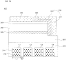
- FIG. 6 is a sectional view showing a light emitting device in accordance with an alternative embodiment.
- the light emitting device 100 in accordance with the alternative embodiment has differences in that the insulating layer 168 is not provided and that the second electrode 180 penetrates the light transmittable electrode layer 150 so as to be connected to the second semiconductor layer 140.
- An empty space between the first electrode 170 and the light emitting structure may prevent short circuit of the light emitting device 100.
- the second electrode 180 may be electrically connected to the second semiconductor layer 140.
- the second electrode 180 may penetrate the light transmittable electrode layer 150 so as to be connected to the second semiconductor layer 140 and may be disposed on the light transmittable electrode layer 150, although the disclosure is not limited thereto.
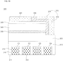
- FIG. 7 is a sectional view showing a light emitting device in accordance with an alternative embodiment.
- the light emitting device 100 in accordance with the alternative embodiment has differences in the shape and height of the first electrode 170 and the second electrode 180.
- the upper surfaces of the first electrode 170 and the second electrode 180 may be disposed higher than the upper surface of the insulating layer 168 such that a spacer 199 is provided on the insulating layer 168.
- the first electrode 170 and the second electrode 180 may be disposed on different partial regions of the upper surface of the insulating layer 168.
- the spacer 199 takes the form of an empty space and may be adjusted in shape and size according to the size and height of the first electrode 170 and the second electrode 180.
- the spacer 199 may have no limit in terms of shape and size and may prevent, e.g., paste or solder from overflowing when the light emitting device 100 is attached using the paste or solder.
- FIG. 8 is a sectional view showing a light emitting device in accordance with an alternative embodiment.
- the light emitting device 200 in accordance with the alternative embodiment has a difference in that an insulating layer 268 is provided.
- the insulating layer 268 may be formed at least from between the lower electrode 272 and the lateral surfaces of the second semiconductor layer 240 and the active layer 230 to between the upper electrode 274 and the second semiconductor layer 240.
- the insulating layer 268 may contain a non-conductive organic material or inorganic material, for example, urethane, polyester or acryl, and may be formed in a single layer or in multiple layers, although the disclosure is not limited thereto.
- the insulating layer 268 may extend up to the same line as the upper surfaces of the first electrode 270 and the second electrode 280.
- the light emitting device 200 is free from short circuit and may achieve enhanced reliability upon flip chip bonding.
- FIG. 9 is a sectional view showing a light emitting device in accordance with an alternative embodiment.
- the light emitting device 100 in accordance with the alternative embodiment further includes a reflective layer 160 and has a difference in the configuration of the second electrode 180.
- the reflective layer 160 may be disposed between the light transmittable electrode layer 150 and the second electrode 180.
- the second electrode 180 may be connected to the light transmittable electrode layer 150 through an opening of the reflective layer 160. That is, the light transmittable electrode layer 150 is disposed on the second semiconductor layer 140, the reflective layer 160 is disposed on the light transmittable electrode layer 150, the second electrode 180 is disposed on the reflective layer 160, and the second electrode 180 and the light transmittable electrode layer 150 are electrically connected to each other.
- the disclosure is not limited thereto, and the second electrode 180 and the light transmittable electrode layer 150 may be connected to each other via various methods.
- the reflective layer 160 in the case in which the light emitting device 100 in accordance with the alternative embodiment is used of a flip chip type, it is possible to enhance light emission efficiency due to high reflectance of the reflective layer 160 and to ensure bonding stability and reliability due to an increased electrode area.
- the reflective layer 160 may include first layers 162 having a first index of refraction and second layers 164 having a second index of refraction that is different from the first index of refraction. That is, the reflective layer 160 may have a configuration in which the layers 162 and 164 having different indices of refraction are alternately stacked one above another.
- the first layers 162 may be layers having a low index of refraction and the second layers 164 may be layers having a high index of refraction, although the disclosure is not limited thereto.
- the reflective layer 160 takes the form of a semiconductor stack in which the first layers 162 having a low index of refraction and the second layer 164 having a high index of refraction, which have a thickness of m ⁇ /4n, are alternately stacked one above another to achieve a reflectance of 95% or more with respect to light of a particular wavelength band ⁇ .
- the first layers 162 having a low index of refraction and the second layers 164 having a high index of refraction may have a thickness of ⁇ /4 times a reference wavelength.
- the thickness of each layer 162 and 164 may be in a range of 2 ⁇ to 10 ⁇ m.
- Each layer 162 or 164 of the reflective layer 160 may be formed of M x O y or M x O y N z (M: Metal or Ceramic, O: Oxide, N: Nitride, X, Y, Z: constants).
- the first layers 162 having a low index of refraction may be formed of SiO 2 having an index of refection of 1.4 or Al 2 O 3 having an index of refection of 1.6
- the second layers 164 having a high index of refraction may be formed of TiO 2 having an index of refection of 2.0 or more, although the disclosure is not limited thereto.
- a greater reflectance may be achieved by increasing an index of refraction of a medium between the first layer 162 having a low index of refraction and the second layer 164 having a high index of refraction.
- the reflective layer 160 as described above has a greater band gap energy than an oscillation wavelength and exhibits less light absorption and consequently, greater light reflectance.
- the reflective layer 160 may extend from the upper surface of the second semiconductor layer 140 to the upper surface of the first semiconductor layer 120 along the lateral surface of the second semiconductor layer 140 and the lateral surface of the active layer 130. Accordingly, light extraction efficiency may be maximized.
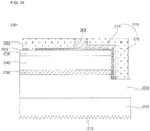
- FIG. 10 is a sectional view showing a light emitting device in accordance with an alternative embodiment.
- the light emitting device 200 in accordance with the embodiment further includes a reflective layer 260 and has a difference in the configuration of the second electrode 280.
- the reflective layer 260 is disposed between the light transmittable electrode layer 250 and the second electrode 280.
- the second electrode 280 may be connected to the light transmittable electrode layer 250 through an opening of the reflective layer 260.
- the light transmittable electrode layer 250 is disposed on the second semiconductor layer 240
- the reflective layer 260 is disposed on the light transmittable electrode layer 250
- the second electrode 280 is disposed on the reflective layer 260
- the second electrode 280 and the light transmittable electrode layer 250 are electrically connected to each other.
- the disclosure is not limited thereto, and the second electrode 280 and the light transmittable electrode layer 250 may be connected to each other via various methods.
- the reflective layer 260 in the case in which the light emitting device 200 in accordance with the alternative embodiment is used in a flip chip type, it is possible to enhance light emission efficiency due to high reflectance of the reflective layer 260 and to ensure bonding stability and reliability due to an increased electrode area.
- the configuration or material of the reflective layer 260 may be as described above.
- FIG. 11 is a sectional view showing emission of light in a configuration in which a light emitting device in accordance with an embodiment is flip chip bonded to a package substrate.
- the principle by which the light emitting device in accordance with the embodiment is flip chip bonded to achieve enhanced light extraction efficiency owing to the reflective layer 160 will be described in detail with reference to FIG. 11 .
- the light emitting device 100 is illustrated as being flip chip bonded onto the package substrate 190.
- the conductor patterns 192 and 194 are formed on the package substrate 190 and are electrically connected to the second electrode 180 and the first electrode 170.
- the wide area electrode which exhibits effective radiation, may be suitable for a high brightness light emitting device.
- the reflective layer 160 formed as described above serves not only to protect the light transmittable electrode layer 150 or the first semiconductor layer 120, but also to prevent light absorption and allow light to be directed to the support member 110, thereby enhancing light extraction efficiency of the light emitting device 100.
- the light emitted from the active layer 130 is reflected by the reflective layer 160 to thereby be wholly directed to the support member 110, which may enhance light emission efficiency of the flip chip type light emitting device 100.
- FIG. 12 is a bottom view showing a light emitting device in accordance with an alternative embodiment
- FIG. 13 is a sectional view of the light emitting device shown in FIG. 12 .
- the light emitting device 300 in accordance with the alternative embodiment includes a support member 310 having a cavity c and the cavity c is filled with a sealing material 314 containing a fluorescent substance 316.
- the cavity c may have various shapes so long as it defines a predetermined space therein and for example, may have a tetragonal, polygonal or circular shape when viewed from the top.
- the cross section of the cavity c may have a cup shape, a concave container shape or the like, and an inner lateral surface of the cavity c may be perpendicular to or inclined from a bottom surface of the cavity c.
- the cavity c may have a circular shape, a tetragonal shape, a polygonal shape, an elliptical shape or the like when viewed from the front, although the disclosure is not limited thereto.
- the front shape of the cavity c may be freely selected.
- the depth h of the cavity c may be in a range of 0.3 to 0.7 times a thickness of the support member 310, although the disclosure is not limited thereto.
- the cavity c may deteriorate rigidity of the support member 310. If the cavity c has an excessively small length L1, it does not provide a sufficient space for white light excitation of light emitted from the active layer 330 and causes deterioration in color rendering because light may be directed to a place where the cavity c is not present. Therefore, the length L1 of the cavity c may be in a range of 0.8 to 0.95 times a length of the support member 310, although the disclosure is not limited thereto.
- the cavity c may deteriorate rigidity of the support member 310. If the cavity c has an excessively small width L2, it does not provide a sufficient space for white light excitation of light emitted from the active layer 330 and causes deterioration in color rendering because light may be directed to a place where the cavity c is not present. Therefore, the width L2 of the cavity c may be in a range of 0.8 to 0.95 times the length of the support member 310, although the disclosure is not limited thereto.
- the cavity c may be opened in the bottom of the support member 310 and may contain the sealing material 314. That is, the cavity c may be filled with and sealed by the sealing material 314.
- the length of the light emitting device 300 may be in a range of 6 to 12 times the thickness of the light emitting device 300, although the disclosure is not limited thereto.
- the sealing material 314 may be a light transmittable resin material, such as silicon or epoxy. After the material is filled in the cavity c, the material may be subjected to ultraviolet or thermal curing, although the disclosure is not limited thereto.
- the sealing material 314 may contain the fluorescent substance 316.
- the kind of the fluorescent substance 316 is selected according to the wavelength of light emitted from the active layer 330, so as to allow the light emitting device 300 to emit white light. Accordingly, the fluorescent substance 316 may include at least one selected from among, for example, red, blue and yellow fluorescent substances, and may include various kinds of fluorescent substances, although the disclosure is not limited thereto.
- the fluorescent substance may be excited by light having a first color that is emitted from the active layer 330 to thereby generate light having a second color.
- the light emitted from the active layer 330 is blue light and the fluorescent substance is a yellow fluorescent substance
- the yellow fluorescent substance may emit white light by being excited by the blue light.
- the light emitted from the active layer 330 is green light
- use of a magenta fluorescent substance or a mixture of blue and red fluorescent substances may be exemplified
- use of a cyan fluorescent substance or a mixture of blue and green fluorescent substances may be exemplified.
- the fluorescent substance 316 may be a known fluorescent substance, such as a YAG-based, TAG-based, sulfide-based, silicate-based, aluminate-based, nitride-based, carbide-based, nitridosilicate-based, borate-based, fluoride-based, phosphate-based fluorescent substance or the like.
- the sealing material 314 may further contain a light diffuser to diffuse light emitted from the active layer 330.
- the light diffuser may be any one of white metal oxides, such as titanium dioxide (TiO 2 ), barium oxide (BaO), silicon dioxide (SiO 2 ), magnesium oxide (MgO) and yttrium oxide (Y 2 O 3 ), or may be a mixture of at least two selected from among titanium dioxide (TiO 2 ), barium oxide (BaO), silicon dioxide (SiO 2 ), magnesium oxide (MgO) and yttrium oxide (Y 2 O 3 ).
- a light diffuser Through use of the light diffuser, irregular reflection of light emitted from the light emitting device may be induced.
- FIG. 14 is a sectional view showing a light emitting device in accordance with an alternative embodiment.
- the light emitting device 300 in accordance with the alternative embodiment has a difference in that the support member 310 has a plurality of cavities c.
- the support member 310 has a plurality of cavities c.
- the cavity c is not limited to a specific number and may be prepared in various numbers according to the size and kind of the light emitting device 300 and the kind of light to be emitted.
- a distance between neighboring cavities may be less than a length of the cavity c, although the disclosure is not limited thereto.
- a difference in the index of refraction between a region having the cavities c and a region having no cavities causes irregular reflection, which may result in enhanced light emission efficiency and color rendering of the light emitting device 300.
- the cavity c may have various shapes so long as it defines a predetermined space therein and for example, may have a tetragonal shape, a polygonal shape or a circular shape when viewed from the top.
- the cross section of the cavity c may have a cup shape, a concave container shape or the like, and an inner lateral surface of the cavity c may be perpendicular to or inclined from a bottom surface of the cavity c.
- the cavity c may have a circular shape, a tetragonal shape, a polygonal shape, an elliptical shape or the like when viewed from the front, although the disclosure is not limited thereto.
- the front shape of the cavity c may be freely selected.
- FIG. 15 is a sectional view showing a light emitting device in accordance with an alternative embodiment
- FIG. 16 is a sectional view showing a light emitting device in accordance with an alternative embodiment.
- the light emitting device 300 in accordance with the alternative embodiment is configured in such a way that uneven patterns 311 and 312 may be formed at a lower surface of the support member 310 or the cavity c.
- the uneven patterns 311 and 312 may be an arrangement of a plurality of semi-spheres, cones and cylinders, which may be arranged regularly or irregularly.
- the uneven patterns 311 and 312 may be formed by etching, more particularly, dry etching or wet etching, although the disclosure is not limited thereto.
- the uneven patterns 311 and 312 serve to induce irregular reflection of light emitted from the active layer 330, thereby enhancing color rendering of the light emitting device 300 and achieving enhanced light extraction efficiency by preventing total reflection of light.
- the light emitting device 300 in accordance with the alternative embodiment is configured in such a way that uneven patterns 311 and 312 may be formed at a lower surface of the support member 310 or the cavity c.
- the uneven patterns 311 and 312 are those as described in FIG. 3 .
- the uneven patterns 311 and 312 induce irregular reflection of light emitted from the active layer 330, thereby enhancing color rendering of the light emitting device 300 and achieving enhanced light extraction efficiency by preventing total reflection of light. Additionally, the uneven patterns 311 and 312 may enhance light emission efficiency,
- FIG. 17 is a sectional view showing a light emitting device in accordance with an alternative embodiment.
- the light emitting device 300 in accordance with the alternative embodiment has a difference in the shape of a lateral surface of the cavity c. Specifically, the length of the cavity c may increase with decreasing distance to a lower surface of the first semiconductor layer 320.
- the length of the cavity c may increase with decreasing distance to the lower surface of the first semiconductor layer 320, thereby providing the cavity c with an inverted trapezoidal cross section.
- the lateral surface of the cavity c is illustrated as having a linear shape, it may have a curvilinear shape or curved surface shape or may be stepped. However, the disclosure is not limited thereto.
- the cavity c Through use of the cavity c, it may be possible to prevent the sealing material 314 from being separated from the support member 310. Also, increasing the length of the cavity c with decreasing distance to the active layer 330 is advantageous to realize white light, and reducing the length of the cavity c at the bottom of the support member 310 may minimize deterioration in the rigidity of the support member 310.
- FIG. 18 is a sectional view showing a light emitting device in accordance with an alternative embodiment.
- the light emitting device 300 in accordance with the embodiment has a difference in the shape of the lateral surface of the cavity c. Specifically, the lateral surface of the cavity c may be stepped.
- the length of the cavity c increases with decreasing distance to the lower surface of the first semiconductor layer 320 and the lateral surface of the cavity c may be stepped.
- the number of steps is not limited and may be determined according to the size and kind of the light emitting device. Also, the steps may have a curvilinear shape or curved surface shape, although the disclosure is not limited thereto.
- the cavity c Through use of the cavity c, it may be possible to prevent the sealing material 314 from being separated from the support member 310. Also, increasing the length of the cavity c with decreasing distance to the active layer 330 is advantageous to realize white light, and reducing the length of the cavity c at the bottom of the support member 310 may minimize deterioration in the rigidity of the support member 310. Moreover, providing the cavity c with the stepped lateral surface may further prevent separation of the sealing material 314 from the support member 310.
- FIG. 19 is a sectional view showing a light emitting device in accordance with an alternative embodiment.
- the light emitting device 300 in accordance with the embodiment has a difference in that the sealing material 314 may include a first sealing material 314a stacked on the bottom of the cavity c and a second sealing material 314b stacked on the first sealing material 314a.
- the first sealing material 314a may contain a light diffuser 318 to diffuse light to be emitted from the light emitting device 300. Both the first sealing material 314a and the second sealing material 314b may contain the fluorescent substance 316. Through use of the light diffuser 318, it may be possible to further enhance color rendering of light emitted from the active layer 330.
- FIG. 20 is a sectional view showing a light emitting device in accordance with an alternative embodiment.
- the light emitting device 300 in accordance with the embodiment may have a difference in that a lower surface of the sealing material 314 may be centrally concave.
- the sealing material 314 may act as a lens to reduce an irradiation angle of light emitted from the active layer 330, which may enhance concentration of the light.
- FIG. 21 is a sectional view showing a light emitting device in accordance with an alternative embodiment.
- the light emitting device 300 in accordance with the alternative embodiment has a difference in that the lower surface of the sealing material 314 may be centrally convex.
- the sealing material 314 may act as a lens to increase an irradiation angle of light emitted from the active layer 330, which may enhance diffusion of the light.
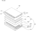
- FIG. 22 is a sectional view of a light emitting device package including a light emitting device in accordance with an embodiment.
- the light emitting device package 500 in accordance with the embodiment may include a body 531, a first electrode layer 538 and a second electrode layer 539 mounted on the body 531, and a light emitting device 536 mounted on the body 531 and electrically connected to the first electrode layer 538 and the second electrode layer 539.
- the light emitting device 536 may be connected in a flip chip manner to the first electrode layer 538 and the second electrode layer 539.
- the body 531 may be formed of a silicon material, a synthetic resin material or a metal material, and the light emitting device 536 may be surrounded by an inclined surface.
- the first electrode layer 538 and the second electrode layer 539 are electrically separated from each other and serve to supply power to the light emitting device 536.
- the first electrode layer 538 and the second electrode layer 539 may serve not only to reflect light emitted from the light emitting device 536, thereby increasing light emission efficiency, but also to discharge heat generated from the light emitting device 536 to the outside.
- a reflective layer 532 may be formed on the body 531, to more effectively concentrate light emitted from the light emitting device 536 forward.
- the reflective layer 532 may be formed of a metal having a high coefficient of reflection, such as silver (Ag), aluminum (Al) and the like.
- an insulating layer 533 may further be formed on the reflective layer 532.
- a cavity 537 is formed in the body 531 such that the light emitting diode 536 is bonded in the cavity 537.
- the cavity 537 may be filled with a molding member to enclose and protect the light emitting diode 536.
- the molding member may contain a fluorescent substance to change a wavelength of light emitted from the light emitting device 536.
- the electrode layers Accordingly, owing to a wide area of the electrode layers, it may be possible to enhance bonding stability and reliability of the light emitting device 536 and to minimize deterioration in the light emission efficiency of the light emitting device 536. Further, the light emitting device 536 may be directly bonded using paste without bumps.
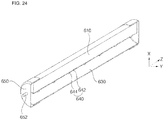
- FIG. 23 is a perspective view showing a lighting apparatus including a light emitting device package in accordance with an embodiment
- FIG. 24 is a sectional view taken along the line C-C' of the lighting apparatus shown in FIG. 23 .
- the lighting apparatus 600 may include a body 610, a cover 630 coupled to the body 610, and end caps 650 disposed at opposite ends of the body 610.
- a light emitting device module 640 may be coupled to a lower surface of the body 610.
- the body 610 may be formed of a metal material having excellent conductivity and heat radiation effects, to discharge heat generated in light emitting device packages 644 to the outside through an upper surface of the body 610.
- the light emitting device packages 644 may have multiple colors and may be arranged in multiple rows on a printed circuit board 642 to form an array. Also, the light emitting device packages 644 may be arranged by the same distance or by different distances as occasion demands, to enable adjustment of brightness.
- the printed circuit board 642 may be formed of a Metal Core PCB (MCPCB), FR4 PCB or the like.
- the light emitting device packages 644 may include a lead frame (not shown) to have an enhanced radiation function. Therefore, the reliability and efficiency of the light emitting device packages 644 may be enhanced, and the lifespan of the lighting apparatus 600 including the light emitting device packages 644 as well as the lifespan of the light emitting device packages 644 may be extended.
- the cover 630 may have a circular shape to surround the lower surface of the body 610, although the disclosure is not limited thereto.
- the cover 630 protects the light emitting device module 640 from external foreign substances, etc.
- the cover 630 may contain diffusive particles to prevent glare of light emitted from the light emitting device packages 644 and to ensure uniform emission of light to the outside.
- a prism pattern may be formed on at least one of an inner surface and an outer surface of the cover 630.
- a fluorescent substance may be applied to at least one of the inner surface and the outer surface of the cover 630.
- the cover 630 must have not only excellent light transmittance, but also heat resistance sufficient to endure heat generated from the light emitting device packages 644.
- the cover 630 may be formed of Polyethylene Terephthalate (PET), Polycarbonate (PC), PolymethylMethacrylate (PMMA) or the like.
- the end caps 650 may be disposed at opposite ends of the body 610 and serve to hermetically seal a power device (not shown).
- the end caps 650 may be provided with power pins 652, which allows the lighting apparatus 600 in accordance with the embodiment to be directly used in a terminal, from which an existing fluorescent lamp has been removed, without requiring a separate device.
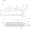
- FIG. 25 is an exploded perspective view of a liquid crystal display apparatus including a light emitting device in accordance with an embodiment.
- FIG. 25 illustrates an edge light type liquid crystal display apparatus 700, which may include a liquid crystal display panel 710 and a backlight unit 770 to irradiate light to the liquid crystal display panel 710.
- the liquid crystal display panel 710 may display an image using light generated from the backlight unit 770.
- the liquid crystal display panel 710 may include a color filter substrate 712 and a thin film transistor substrate 714, which are arranged to face each other with liquid crystals interposed therebetween.
- the color filter substrate 312 may realize the color of the image displayed via the liquid crystal display panel 710.
- the thin film transistor substrate 714 is electrically connected to a printed circuit board 718, on which a plurality of circuit elements is mounted, by means of a drive film 717.
- the thin film transistor substrate 714 may apply drive voltage, provided by the printed circuit board 718, to the liquid crystals in response to a drive signal transmitted from the printed circuit board 718.
- the thin film transistor substrate 714 may include pixel electrodes and thin film transistors in the form of thin films formed on another substrate formed of a transparent material, such as glass, plastic or the like.
- the backlight unit 770 includes a light emitting device module 720 to emit light, a light guide plate 730 to change light emitted from the light emitting device module 720 into planar light and transmit the planar light to the liquid crystal display panel 710, a plurality of films 750, 760 and 764 to achieve uniformity in brightness distribution and improve vertical light incidence of the light having passed through the light guide plate 730, and a reflective sheet 740 to reflect light, emitted rearward from the light guide plate 730, toward the light guide plate 730.
- the light emitting device module 720 may include a plurality of light emitting device packages 724 and a printed circuit board 722 on which the plurality of light emitting device packages 724 is mounted to define an array.
- the backlight unit 770 may include a diffusive film 766, which diffuses incident light from the liquid guide plate 730 toward the liquid display panel 710, and a prism film 750 which condenses the diffused light to enhance vertical incidence.
- the prism film 750 may include a protective film 764 to protect the prism film 750.
- FIG. 26 is an exploded perspective view of a liquid crystal display apparatus including a light emitting device in accordance with an embodiment. The same configuration as that illustrated and described in FIG. 25 will not be repeated hereinafter.
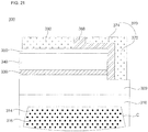
- FIG. 26 illustrates a vertical type liquid crystal display apparatus 800, which may include a liquid crystal display panel 810 and a backlight unit 870 to irradiate light to the liquid crystal display panel 810.
- the liquid crystal display panel 810 is identical to the description with reference to FIG. 25 and thus, a detailed description thereof will be omitted.
- the backlight unit 870 may include a plurality of light emitting device modules 823, a reflective sheet 824, a lower chassis 830 in which the light emitting device modules 823 and the reflective sheet 824 are accommodated, a diffusive plate 840 and a plurality of optical films 860 disposed above the light emitting device modules 823.
- Each of the light emitting device modules 823 may include a plurality of light emitting device packages 822 and a printed circuit board 821 on which the plurality of light emitting device packages 822 is mounted to form an array.
- the reflective sheet 824 serves to reflect light emitted from the light emitting device packages 822 toward the liquid crystal display panel 810, thereby improving use efficiency of the light.
- the light emitted from the light emitting device modules 823 is introduced into the diffusive plate 840, and optical films 860 are disposed above the diffusive plate 840.
- the optical films 860 may include a diffusive film 866, a prism film 850 and a protective film 864.
- the embodiments provide a flip chip type light emitting device, which achieves enhanced light emission efficiency as well as stability and reliability upon bonding to a light emitting device package.
- the flip chip type light emitting device does not need separate bumps upon bonding, which may result in reduction in production costs and time.
Claims (12)
- Dispositif luminescent comprenant :un élément de support (110 ; 210) ;une structure luminescente incluant une première couche semi-conductrice (120 ; 220) disposée sur l'élément de support, une seconde couche semi-conductrice (140 ; 240) et une couche active (130 ; 230) entre la première couche semi-conductrice et la seconde couche semi-conductrice ;une première électrode (170 ; 270) disposée sur la première couche semi-conductrice (120 ; 220) dans une première région à travers laquelle est exposée la première couche semi-conductrice ;une seconde électrode (180 ; 280) disposée sur la seconde couche semi-conductrice (140 ; 240) ;une couche isolante (168 ; 268) disposée au moins entre la première électrode (170 ; 270) et la structure luminescente ;une couche d'électrode transmettant la lumière (150 ; 250) disposée entre la seconde couche semi-conductrice (140 ; 240) et la seconde électrode (180 ; 280) ; etune couche réfléchissante (160 ; 260) entre la couche d'électrode transmettant la lumière (150 ; 250) et la seconde électrode (180 ; 280),dans lequel la première couche semi-conductrice (120 ; 220) et la seconde couche semi-conductrice (140 ; 240) sont des couches semi-conductrices conductrices différentes, la couche active (130 ; 230) inclut au moins une paire formée d'une couche puits et d'une couche barrière, et la couche puits présente une bande interdite plus petite que la couche barrière, etdans lequel la seconde électrode (180 ; 280) est connectée à la couche d'électrode transmettant la lumière (150 ; 250) à travers une ouverture de la couche réfléchissante (160 ; 260),caractérisé en ce que la couche réfléchissante (160 ; 260) est formée à partir d'une surface supérieure de la seconde couche semi-conductrice (140 ; 240) jusqu'à une surface supérieure de la première couche semi-conductrice (120 ; 220) le long d'une surface latérale de la seconde couche semi-conductrice et d'une surface latérale de la couche active (130 ; 330),la couche d'électrode transmettant la lumière (150) est en contact avec la seconde couche semi-conductrice (140), la couche réfléchissante (160) en contact avec la couche d'électrode transmettant la lumière (150), la seconde électrode (180) est en contact avec la couche réfléchissante (160) et la couche d'électrode transmettant la lumière (150)et en ce qu'une superficie d'une surface supérieure de la première électrode (170 ; 270) est dans une plage de 40 % à 90 % d'une superficie de la seconde couche semi-conductrice (140 ; 240).
- Dispositif luminescent selon la revendication 1,
dans lequel la première électrode (270) inclut :une électrode inférieure (272) connectée à la première couche semi-conductrice (220) et formée pour s'étendre au moins jusqu'à une hauteur de la seconde couche semi-conductrice (240) ; etune électrode supérieure (274) connectée à une extrémité de l'électrode inférieure et configurée pour faire saillie vers l'intérieur de la structure luminescente de telle sorte qu'une région partielle de l'électrode supérieure chevauche verticalement la seconde couche semi-conductrice, l'électrode supérieure étant espacée d'une surface supérieure de la seconde couche semi-conductrice, etdans lequel une superficie de l'électrode inférieure (272) vue depuis le haut est dans une plage de 10 % à 50 % d'une superficie de l'électrode supérieure (274). - Dispositif luminescent selon la revendication 1 ou 2,
dans lequel la surface supérieure et une surface inférieure de la première électrode (170 ; 270) présentent des superficies différentes. - Dispositif luminescent selon l'une quelconque des revendications 1 à 3,
dans lequel la surface supérieure de la première électrode (170 ; 270) et une surface supérieure de la seconde électrode (180 ; 280) sont disposées sur la même ligne. - Dispositif luminescent selon la revendication 4,
dans lequel la couche isolante (168 ; 268) est formée depuis entre la première électrode (170 ; 270) et des surfaces latérales de la seconde couche semi-conductrice (140 ; 240) et de la couche active (130 ; 230) et jusqu'à la même ligne que les surfaces supérieures de la première électrode (170 ; 270) et de la seconde électrode (180 ; 280). - Dispositif luminescent selon la revendication 2,
dans lequel la couche isolante (268) est formée au moins depuis entre l'électrode inférieure (272) et des surfaces latérales de la seconde couche semi-conductrice (240) et de la couche active (230) jusqu'entre l'électrode supérieure (274) et la seconde couche semi-conductrice. - Dispositif luminescent selon la revendication 6,
dans lequel les surfaces supérieures de la première électrode (170) et de la seconde électrode (180) sont disposées plus haut qu'une surface supérieure de la couche isolante (168), et
dans lequel le dispositif luminescent (100) comprend en outre un séparateur (199) disposé sur la couche isolante (168) dans un intervalle entre la première électrode (170) et la seconde électrode (180). - Dispositif luminescent selon la revendication 7,
dans lequel le séparateur prend la forme d'un espace vide (199). - Dispositif luminescent selon la revendication 8,
dans lequel le séparateur (199) comporte une surface supérieure qui est coplanaire avec les surfaces supérieures de la première électrode (170) et de la seconde électrode (180). - Dispositif luminescent selon l'une quelconque des revendications précédentes,
dans lequel la couche isolante (168 ; 268) comprend un matériau organique. - Dispositif luminescent selon la revendication 10,
dans lequel la couche isolante (168 ; 268) est formée d'uréthane, de polyester ou d'acryle. - Composant à dispositif luminescent, comprenant :un substrat de composant (190) ; etun dispositif luminescent (100) selon l'une quelconque des revendications précédentes, soudé tête-bêche sans bosses sur le substrat de composant (190).
Applications Claiming Priority (2)
| Application Number | Priority Date | Filing Date | Title |
|---|---|---|---|
| KR1020110102986A KR20130038558A (ko) | 2011-10-10 | 2011-10-10 | 발광소자 |
| KR1020110104233A KR20130039574A (ko) | 2011-10-12 | 2011-10-12 | 발광소자 |
Publications (3)
| Publication Number | Publication Date |
|---|---|
| EP2581953A2 EP2581953A2 (fr) | 2013-04-17 |
| EP2581953A3 EP2581953A3 (fr) | 2013-05-29 |
| EP2581953B1 true EP2581953B1 (fr) | 2020-04-08 |
Family
ID=45562246
Family Applications (1)
| Application Number | Title | Priority Date | Filing Date |
|---|---|---|---|
| EP12155005.7A Active EP2581953B1 (fr) | 2011-10-10 | 2012-02-10 | Dispositif électroluminescent |
Country Status (4)
| Country | Link |
|---|---|
| US (1) | US8785952B2 (fr) |
| EP (1) | EP2581953B1 (fr) |
| JP (1) | JP2013084881A (fr) |
| CN (1) | CN103035809B (fr) |
Families Citing this family (16)
| Publication number | Priority date | Publication date | Assignee | Title |
|---|---|---|---|---|
| WO2013134432A1 (fr) * | 2012-03-06 | 2013-09-12 | Soraa, Inc. | Diodes électroluminescentes à couches de matériau à faible indice de réfraction destinées à réduire des effets de guidage de lumière |
| US20140362603A1 (en) | 2013-05-09 | 2014-12-11 | Seoul Semiconductor Co., Ltd. | Light source module and backlight unit having the same |
| CN103456729B (zh) * | 2013-07-26 | 2016-09-21 | 利亚德光电股份有限公司 | 发光二极管显示屏 |
| JP6511757B2 (ja) * | 2014-09-30 | 2019-05-15 | 日亜化学工業株式会社 | 発光装置 |
| JP6527695B2 (ja) * | 2014-12-22 | 2019-06-05 | スタンレー電気株式会社 | 半導体発光装置 |
| JP2016163015A (ja) * | 2015-03-05 | 2016-09-05 | 旭化成株式会社 | 紫外線発光素子及びその製造方法 |
| KR101688163B1 (ko) * | 2015-03-30 | 2016-12-20 | 엘지전자 주식회사 | 반도체 발광 소자를 이용한 디스플레이 장치 및 이의 제조방법 |
| DE102015112538B4 (de) * | 2015-07-30 | 2023-08-03 | OSRAM Opto Semiconductors Gesellschaft mit beschränkter Haftung | Optoelektronisches Bauelement und ein Verfahren zur Herstellung eines optoelektronischen Bauelements |
| US10361346B2 (en) | 2015-10-27 | 2019-07-23 | Soko Kagaku Co., Ltd. | Nitride semiconductor ultraviolet light emitting device and method for manufacturing same |
| JP2017112321A (ja) * | 2015-12-18 | 2017-06-22 | ソニー株式会社 | 発光ユニットおよび表示装置 |
| TW201727894A (zh) * | 2016-01-18 | 2017-08-01 | Nat Univ Tsing Hua | 具有垂直型跨接結構電極的水平式半導體元件 |
| US10332949B2 (en) * | 2016-07-06 | 2019-06-25 | Seoul Semiconductor Co., Ltd. | Display apparatus |
| CN109216522B (zh) * | 2017-07-07 | 2020-02-07 | 鸿富锦精密工业(深圳)有限公司 | 微型led显示面板 |
| KR102474953B1 (ko) | 2018-03-22 | 2022-12-06 | 엘지이노텍 주식회사 | 반도체 소자 |
| US11848398B2 (en) * | 2019-12-29 | 2023-12-19 | Seoul Viosys Co., Ltd. | Flat bonding method of light emitting device and flat bonder for light emitting device |
| CN113066805B (zh) * | 2021-03-23 | 2023-01-10 | 京东方科技集团股份有限公司 | 显示装置、显示面板、驱动背板及其制造方法 |
Family Cites Families (23)
| Publication number | Priority date | Publication date | Assignee | Title |
|---|---|---|---|---|
| JP4203132B2 (ja) * | 1997-03-31 | 2008-12-24 | シャープ株式会社 | 発光素子及びその製造方法 |
| JP3896704B2 (ja) * | 1998-10-07 | 2007-03-22 | 松下電器産業株式会社 | GaN系化合物半導体発光素子 |
| JP4418057B2 (ja) * | 1999-09-14 | 2010-02-17 | 星和電機株式会社 | Ledチップ |
| US6630689B2 (en) | 2001-05-09 | 2003-10-07 | Lumileds Lighting, U.S. Llc | Semiconductor LED flip-chip with high reflectivity dielectric coating on the mesa |
| JP4822482B2 (ja) * | 2001-05-23 | 2011-11-24 | シチズン電子株式会社 | 発光ダイオードおよびその製造方法 |
| JP4214704B2 (ja) * | 2002-03-20 | 2009-01-28 | 日亜化学工業株式会社 | 半導体素子 |
| KR100499129B1 (ko) * | 2002-09-02 | 2005-07-04 | 삼성전기주식회사 | 발광 다이오드 및 그 제조방법 |
| KR100543696B1 (ko) * | 2002-09-09 | 2006-01-20 | 삼성전기주식회사 | 고효율 발광 다이오드 |
| JP2005197573A (ja) * | 2004-01-09 | 2005-07-21 | Sharp Corp | Iii族窒化物半導体発光素子 |
| JP4121536B2 (ja) * | 2004-09-27 | 2008-07-23 | 松下電器産業株式会社 | 半導体発光素子、その製造方法及びその実装方法、並びに発光装置 |
| JP4614773B2 (ja) * | 2005-01-11 | 2011-01-19 | パナソニック株式会社 | 半導体発光装置 |
| TWI244228B (en) | 2005-02-03 | 2005-11-21 | United Epitaxy Co Ltd | Light emitting device and manufacture method thereof |
| JP5008262B2 (ja) * | 2005-03-02 | 2012-08-22 | 日亜化学工業株式会社 | 半導体発光素子 |
| CN100454592C (zh) * | 2005-07-06 | 2009-01-21 | 晶元光电股份有限公司 | 半导体发光元件 |
| JP2007173269A (ja) * | 2005-12-19 | 2007-07-05 | Showa Denko Kk | フリップチップ型半導体発光素子、フリップチップ型半導体発光素子の製造方法、フリップチップ型半導体発光素子の実装構造及び発光ダイオードランプ |
| US8158990B2 (en) * | 2006-10-05 | 2012-04-17 | Mitsubishi Chemical Corporation | Light emitting device using GaN LED chip |
| JP2009164423A (ja) * | 2008-01-08 | 2009-07-23 | Nichia Corp | 発光素子 |
| WO2009125953A2 (fr) | 2008-04-06 | 2009-10-15 | Song June O | Élément lumineux |
| JP2010087292A (ja) * | 2008-09-30 | 2010-04-15 | Toyoda Gosei Co Ltd | 発光素子 |
| JP5152133B2 (ja) * | 2009-09-18 | 2013-02-27 | 豊田合成株式会社 | 発光素子 |
| JP2011119491A (ja) * | 2009-12-04 | 2011-06-16 | Showa Denko Kk | 半導体発光素子、電子機器および発光装置 |
| CN102884645B (zh) * | 2010-01-29 | 2015-05-27 | 西铁城电子株式会社 | 发光装置的制造方法以及发光装置 |
| JP5381853B2 (ja) * | 2010-03-26 | 2014-01-08 | 豊田合成株式会社 | 半導体発光素子 |
-
2012
- 2012-02-06 US US13/366,991 patent/US8785952B2/en active Active
- 2012-02-10 EP EP12155005.7A patent/EP2581953B1/fr active Active
- 2012-03-05 CN CN201210055541.5A patent/CN103035809B/zh active Active
- 2012-03-07 JP JP2012051012A patent/JP2013084881A/ja active Pending
Non-Patent Citations (1)
| Title |
|---|
| None * |
Also Published As
| Publication number | Publication date |
|---|---|
| US20120132946A1 (en) | 2012-05-31 |
| JP2013084881A (ja) | 2013-05-09 |
| EP2581953A3 (fr) | 2013-05-29 |
| CN103035809A (zh) | 2013-04-10 |
| CN103035809B (zh) | 2017-06-20 |
| EP2581953A2 (fr) | 2013-04-17 |
| US8785952B2 (en) | 2014-07-22 |
Similar Documents
| Publication | Publication Date | Title |
|---|---|---|
| EP2581953B1 (fr) | Dispositif électroluminescent | |
| EP2369648B1 (fr) | Dispositif électroluminescent | |
| EP2388835B1 (fr) | Configuration d'électrodes pour une diode électroluminescente | |
| EP2551923B1 (fr) | Diode électroluminescente | |
| EP2369643B1 (fr) | Diode électroluminescente | |
| EP2388839B1 (fr) | Dispositif luminescent avec couche de conversion entre une couche réfléchissante et les couches d'une diode électroluminescente | |
| US9343629B2 (en) | Light emitting device | |
| US9455371B2 (en) | Light emitting device | |
| US8759853B2 (en) | Light emitting device | |
| US20130105761A1 (en) | Light emitting device and method for manufacturing the same | |
| EP2405496A2 (fr) | Dispositif électroluminescent avec une face N entre deux couches semiconductrices de type-n. | |
| KR101746002B1 (ko) | 발광소자 | |
| US8445924B2 (en) | Light emitting device | |
| KR20120045536A (ko) | 발광소자 및 이의 제조방법 | |
| EP2605293A2 (fr) | Dispositif électroluminescent | |
| KR20130038558A (ko) | 발광소자 | |
| KR20130039574A (ko) | 발광소자 | |
| KR101843726B1 (ko) | 발광소자 | |
| KR20130009899A (ko) | 발광소자 |
Legal Events
| Date | Code | Title | Description |
|---|---|---|---|
| PUAI | Public reference made under article 153(3) epc to a published international application that has entered the european phase |
Free format text: ORIGINAL CODE: 0009012 |
|
| AK | Designated contracting states |
Kind code of ref document: A2 Designated state(s): AL AT BE BG CH CY CZ DE DK EE ES FI FR GB GR HR HU IE IS IT LI LT LU LV MC MK MT NL NO PL PT RO RS SE SI SK SM TR |
|
| AX | Request for extension of the european patent |
Extension state: BA ME |
|
| PUAL | Search report despatched |
Free format text: ORIGINAL CODE: 0009013 |
|
| AK | Designated contracting states |
Kind code of ref document: A3 Designated state(s): AL AT BE BG CH CY CZ DE DK EE ES FI FR GB GR HR HU IE IS IT LI LT LU LV MC MK MT NL NO PL PT RO RS SE SI SK SM TR |
|
| AX | Request for extension of the european patent |
Extension state: BA ME |
|
| RIC1 | Information provided on ipc code assigned before grant |
Ipc: H01L 33/44 20100101AFI20130424BHEP |
|
| 17P | Request for examination filed |
Effective date: 20131128 |
|
| RBV | Designated contracting states (corrected) |
Designated state(s): AL AT BE BG CH CY CZ DE DK EE ES FI FR GB GR HR HU IE IS IT LI LT LU LV MC MK MT NL NO PL PT RO RS SE SI SK SM TR |
|
| RAP1 | Party data changed (applicant data changed or rights of an application transferred) |
Owner name: LG INNOTEK CO., LTD. |
|
| RAP1 | Party data changed (applicant data changed or rights of an application transferred) |
Owner name: LG INNOTEK CO., LTD. |
|
| STAA | Information on the status of an ep patent application or granted ep patent |
Free format text: STATUS: EXAMINATION IS IN PROGRESS |
|
| 17Q | First examination report despatched |
Effective date: 20180719 |
|
| REG | Reference to a national code |
Ref country code: DE Ref legal event code: R079 Ref document number: 602012069045 Country of ref document: DE Free format text: PREVIOUS MAIN CLASS: H01L0033440000 Ipc: H01L0033620000 |
|
| GRAP | Despatch of communication of intention to grant a patent |
Free format text: ORIGINAL CODE: EPIDOSNIGR1 |
|
| STAA | Information on the status of an ep patent application or granted ep patent |
Free format text: STATUS: GRANT OF PATENT IS INTENDED |
|
| RIC1 | Information provided on ipc code assigned before grant |
Ipc: H01L 33/44 20100101ALI20191022BHEP Ipc: H01L 33/62 20100101AFI20191022BHEP |
|
| INTG | Intention to grant announced |
Effective date: 20191126 |
|
| GRAS | Grant fee paid |
Free format text: ORIGINAL CODE: EPIDOSNIGR3 |
|
| GRAA | (expected) grant |
Free format text: ORIGINAL CODE: 0009210 |
|
| STAA | Information on the status of an ep patent application or granted ep patent |
Free format text: STATUS: THE PATENT HAS BEEN GRANTED |
|
| AK | Designated contracting states |
Kind code of ref document: B1 Designated state(s): AL AT BE BG CH CY CZ DE DK EE ES FI FR GB GR HR HU IE IS IT LI LT LU LV MC MK MT NL NO PL PT RO RS SE SI SK SM TR |
|
| REG | Reference to a national code |
Ref country code: GB Ref legal event code: FG4D |
|
| REG | Reference to a national code |
Ref country code: AT Ref legal event code: REF Ref document number: 1255555 Country of ref document: AT Kind code of ref document: T Effective date: 20200415 Ref country code: CH Ref legal event code: EP |
|
| REG | Reference to a national code |
Ref country code: DE Ref legal event code: R096 Ref document number: 602012069045 Country of ref document: DE |
|
| REG | Reference to a national code |
Ref country code: IE Ref legal event code: FG4D |
|
| REG | Reference to a national code |
Ref country code: NL Ref legal event code: MP Effective date: 20200408 |
|
| REG | Reference to a national code |
Ref country code: LT Ref legal event code: MG4D |
|
| PG25 | Lapsed in a contracting state [announced via postgrant information from national office to epo] |
Ref country code: GR Free format text: LAPSE BECAUSE OF FAILURE TO SUBMIT A TRANSLATION OF THE DESCRIPTION OR TO PAY THE FEE WITHIN THE PRESCRIBED TIME-LIMIT Effective date: 20200709 Ref country code: NO Free format text: LAPSE BECAUSE OF FAILURE TO SUBMIT A TRANSLATION OF THE DESCRIPTION OR TO PAY THE FEE WITHIN THE PRESCRIBED TIME-LIMIT Effective date: 20200708 Ref country code: SE Free format text: LAPSE BECAUSE OF FAILURE TO SUBMIT A TRANSLATION OF THE DESCRIPTION OR TO PAY THE FEE WITHIN THE PRESCRIBED TIME-LIMIT Effective date: 20200408 Ref country code: IS Free format text: LAPSE BECAUSE OF FAILURE TO SUBMIT A TRANSLATION OF THE DESCRIPTION OR TO PAY THE FEE WITHIN THE PRESCRIBED TIME-LIMIT Effective date: 20200808 Ref country code: PT Free format text: LAPSE BECAUSE OF FAILURE TO SUBMIT A TRANSLATION OF THE DESCRIPTION OR TO PAY THE FEE WITHIN THE PRESCRIBED TIME-LIMIT Effective date: 20200817 Ref country code: NL Free format text: LAPSE BECAUSE OF FAILURE TO SUBMIT A TRANSLATION OF THE DESCRIPTION OR TO PAY THE FEE WITHIN THE PRESCRIBED TIME-LIMIT Effective date: 20200408 Ref country code: FI Free format text: LAPSE BECAUSE OF FAILURE TO SUBMIT A TRANSLATION OF THE DESCRIPTION OR TO PAY THE FEE WITHIN THE PRESCRIBED TIME-LIMIT Effective date: 20200408 Ref country code: LT Free format text: LAPSE BECAUSE OF FAILURE TO SUBMIT A TRANSLATION OF THE DESCRIPTION OR TO PAY THE FEE WITHIN THE PRESCRIBED TIME-LIMIT Effective date: 20200408 |
|
| REG | Reference to a national code |
Ref country code: AT Ref legal event code: MK05 Ref document number: 1255555 Country of ref document: AT Kind code of ref document: T Effective date: 20200408 |
|
| PG25 | Lapsed in a contracting state [announced via postgrant information from national office to epo] |
Ref country code: HR Free format text: LAPSE BECAUSE OF FAILURE TO SUBMIT A TRANSLATION OF THE DESCRIPTION OR TO PAY THE FEE WITHIN THE PRESCRIBED TIME-LIMIT Effective date: 20200408 Ref country code: LV Free format text: LAPSE BECAUSE OF FAILURE TO SUBMIT A TRANSLATION OF THE DESCRIPTION OR TO PAY THE FEE WITHIN THE PRESCRIBED TIME-LIMIT Effective date: 20200408 Ref country code: RS Free format text: LAPSE BECAUSE OF FAILURE TO SUBMIT A TRANSLATION OF THE DESCRIPTION OR TO PAY THE FEE WITHIN THE PRESCRIBED TIME-LIMIT Effective date: 20200408 Ref country code: BG Free format text: LAPSE BECAUSE OF FAILURE TO SUBMIT A TRANSLATION OF THE DESCRIPTION OR TO PAY THE FEE WITHIN THE PRESCRIBED TIME-LIMIT Effective date: 20200708 |
|
| PG25 | Lapsed in a contracting state [announced via postgrant information from national office to epo] |
Ref country code: AL Free format text: LAPSE BECAUSE OF FAILURE TO SUBMIT A TRANSLATION OF THE DESCRIPTION OR TO PAY THE FEE WITHIN THE PRESCRIBED TIME-LIMIT Effective date: 20200408 |
|
| REG | Reference to a national code |
Ref country code: DE Ref legal event code: R097 Ref document number: 602012069045 Country of ref document: DE |
|
| PG25 | Lapsed in a contracting state [announced via postgrant information from national office to epo] |
Ref country code: ES Free format text: LAPSE BECAUSE OF FAILURE TO SUBMIT A TRANSLATION OF THE DESCRIPTION OR TO PAY THE FEE WITHIN THE PRESCRIBED TIME-LIMIT Effective date: 20200408 Ref country code: CZ Free format text: LAPSE BECAUSE OF FAILURE TO SUBMIT A TRANSLATION OF THE DESCRIPTION OR TO PAY THE FEE WITHIN THE PRESCRIBED TIME-LIMIT Effective date: 20200408 Ref country code: AT Free format text: LAPSE BECAUSE OF FAILURE TO SUBMIT A TRANSLATION OF THE DESCRIPTION OR TO PAY THE FEE WITHIN THE PRESCRIBED TIME-LIMIT Effective date: 20200408 Ref country code: RO Free format text: LAPSE BECAUSE OF FAILURE TO SUBMIT A TRANSLATION OF THE DESCRIPTION OR TO PAY THE FEE WITHIN THE PRESCRIBED TIME-LIMIT Effective date: 20200408 Ref country code: IT Free format text: LAPSE BECAUSE OF FAILURE TO SUBMIT A TRANSLATION OF THE DESCRIPTION OR TO PAY THE FEE WITHIN THE PRESCRIBED TIME-LIMIT Effective date: 20200408 Ref country code: DK Free format text: LAPSE BECAUSE OF FAILURE TO SUBMIT A TRANSLATION OF THE DESCRIPTION OR TO PAY THE FEE WITHIN THE PRESCRIBED TIME-LIMIT Effective date: 20200408 Ref country code: EE Free format text: LAPSE BECAUSE OF FAILURE TO SUBMIT A TRANSLATION OF THE DESCRIPTION OR TO PAY THE FEE WITHIN THE PRESCRIBED TIME-LIMIT Effective date: 20200408 Ref country code: SM Free format text: LAPSE BECAUSE OF FAILURE TO SUBMIT A TRANSLATION OF THE DESCRIPTION OR TO PAY THE FEE WITHIN THE PRESCRIBED TIME-LIMIT Effective date: 20200408 |
|
| PLBE | No opposition filed within time limit |
Free format text: ORIGINAL CODE: 0009261 |
|
| STAA | Information on the status of an ep patent application or granted ep patent |
Free format text: STATUS: NO OPPOSITION FILED WITHIN TIME LIMIT |
|
| PG25 | Lapsed in a contracting state [announced via postgrant information from national office to epo] |
Ref country code: SK Free format text: LAPSE BECAUSE OF FAILURE TO SUBMIT A TRANSLATION OF THE DESCRIPTION OR TO PAY THE FEE WITHIN THE PRESCRIBED TIME-LIMIT Effective date: 20200408 Ref country code: PL Free format text: LAPSE BECAUSE OF FAILURE TO SUBMIT A TRANSLATION OF THE DESCRIPTION OR TO PAY THE FEE WITHIN THE PRESCRIBED TIME-LIMIT Effective date: 20200408 |
|
| 26N | No opposition filed |
Effective date: 20210112 |
|
| PG25 | Lapsed in a contracting state [announced via postgrant information from national office to epo] |
Ref country code: SI Free format text: LAPSE BECAUSE OF FAILURE TO SUBMIT A TRANSLATION OF THE DESCRIPTION OR TO PAY THE FEE WITHIN THE PRESCRIBED TIME-LIMIT Effective date: 20200408 |
|
| REG | Reference to a national code |
Ref country code: DE Ref legal event code: R081 Ref document number: 602012069045 Country of ref document: DE Owner name: SUZHOU LEKIN SEMICONDUCTOR CO. LTD., TAICANG, CN Free format text: FORMER OWNER: LG INNOTEK CO., LTD., SEOUL, KR |
|
| PG25 | Lapsed in a contracting state [announced via postgrant information from national office to epo] |
Ref country code: MC Free format text: LAPSE BECAUSE OF FAILURE TO SUBMIT A TRANSLATION OF THE DESCRIPTION OR TO PAY THE FEE WITHIN THE PRESCRIBED TIME-LIMIT Effective date: 20200408 |
|
| GBPC | Gb: european patent ceased through non-payment of renewal fee |
Effective date: 20210210 |
|
| REG | Reference to a national code |
Ref country code: BE Ref legal event code: MM Effective date: 20210228 |
|
| PG25 | Lapsed in a contracting state [announced via postgrant information from national office to epo] |
Ref country code: LU Free format text: LAPSE BECAUSE OF NON-PAYMENT OF DUE FEES Effective date: 20210210 Ref country code: LI Free format text: LAPSE BECAUSE OF NON-PAYMENT OF DUE FEES Effective date: 20210228 Ref country code: CH Free format text: LAPSE BECAUSE OF NON-PAYMENT OF DUE FEES Effective date: 20210228 |
|
| PG25 | Lapsed in a contracting state [announced via postgrant information from national office to epo] |
Ref country code: GB Free format text: LAPSE BECAUSE OF NON-PAYMENT OF DUE FEES Effective date: 20210210 Ref country code: IE Free format text: LAPSE BECAUSE OF NON-PAYMENT OF DUE FEES Effective date: 20210210 Ref country code: FR Free format text: LAPSE BECAUSE OF NON-PAYMENT OF DUE FEES Effective date: 20210228 |
|
| PG25 | Lapsed in a contracting state [announced via postgrant information from national office to epo] |
Ref country code: BE Free format text: LAPSE BECAUSE OF NON-PAYMENT OF DUE FEES Effective date: 20210228 |
|
| PG25 | Lapsed in a contracting state [announced via postgrant information from national office to epo] |
Ref country code: HU Free format text: LAPSE BECAUSE OF FAILURE TO SUBMIT A TRANSLATION OF THE DESCRIPTION OR TO PAY THE FEE WITHIN THE PRESCRIBED TIME-LIMIT; INVALID AB INITIO Effective date: 20120210 Ref country code: CY Free format text: LAPSE BECAUSE OF FAILURE TO SUBMIT A TRANSLATION OF THE DESCRIPTION OR TO PAY THE FEE WITHIN THE PRESCRIBED TIME-LIMIT Effective date: 20200408 |
|
| PG25 | Lapsed in a contracting state [announced via postgrant information from national office to epo] |
Ref country code: MK Free format text: LAPSE BECAUSE OF FAILURE TO SUBMIT A TRANSLATION OF THE DESCRIPTION OR TO PAY THE FEE WITHIN THE PRESCRIBED TIME-LIMIT Effective date: 20200408 |
|
| PGFP | Annual fee paid to national office [announced via postgrant information from national office to epo] |
Ref country code: DE Payment date: 20231220 Year of fee payment: 13 |