EP2581953B1 - Light emitting device - Google Patents
Light emitting device Download PDFInfo
- Publication number
- EP2581953B1 EP2581953B1 EP12155005.7A EP12155005A EP2581953B1 EP 2581953 B1 EP2581953 B1 EP 2581953B1 EP 12155005 A EP12155005 A EP 12155005A EP 2581953 B1 EP2581953 B1 EP 2581953B1
- Authority
- EP
- European Patent Office
- Prior art keywords
- electrode
- light emitting
- layer
- emitting device
- semiconductor layer
- Prior art date
- Legal status (The legal status is an assumption and is not a legal conclusion. Google has not performed a legal analysis and makes no representation as to the accuracy of the status listed.)
- Active
Links
Images


Classifications
-
- H—ELECTRICITY
- H01—ELECTRIC ELEMENTS
- H01L—SEMICONDUCTOR DEVICES NOT COVERED BY CLASS H10
- H01L33/00—Semiconductor devices with at least one potential-jump barrier or surface barrier specially adapted for light emission; Processes or apparatus specially adapted for the manufacture or treatment thereof or of parts thereof; Details thereof
- H01L33/44—Semiconductor devices with at least one potential-jump barrier or surface barrier specially adapted for light emission; Processes or apparatus specially adapted for the manufacture or treatment thereof or of parts thereof; Details thereof characterised by the coatings, e.g. passivation layer or anti-reflective coating
-
- H—ELECTRICITY
- H01—ELECTRIC ELEMENTS
- H01L—SEMICONDUCTOR DEVICES NOT COVERED BY CLASS H10
- H01L2924/00—Indexing scheme for arrangements or methods for connecting or disconnecting semiconductor or solid-state bodies as covered by H01L24/00
- H01L2924/0001—Technical content checked by a classifier
- H01L2924/0002—Not covered by any one of groups H01L24/00, H01L24/00 and H01L2224/00
-
- H—ELECTRICITY
- H01—ELECTRIC ELEMENTS
- H01L—SEMICONDUCTOR DEVICES NOT COVERED BY CLASS H10
- H01L33/00—Semiconductor devices with at least one potential-jump barrier or surface barrier specially adapted for light emission; Processes or apparatus specially adapted for the manufacture or treatment thereof or of parts thereof; Details thereof
- H01L33/02—Semiconductor devices with at least one potential-jump barrier or surface barrier specially adapted for light emission; Processes or apparatus specially adapted for the manufacture or treatment thereof or of parts thereof; Details thereof characterised by the semiconductor bodies
- H01L33/08—Semiconductor devices with at least one potential-jump barrier or surface barrier specially adapted for light emission; Processes or apparatus specially adapted for the manufacture or treatment thereof or of parts thereof; Details thereof characterised by the semiconductor bodies with a plurality of light emitting regions, e.g. laterally discontinuous light emitting layer or photoluminescent region integrated within the semiconductor body
-
- H—ELECTRICITY
- H01—ELECTRIC ELEMENTS
- H01L—SEMICONDUCTOR DEVICES NOT COVERED BY CLASS H10
- H01L33/00—Semiconductor devices with at least one potential-jump barrier or surface barrier specially adapted for light emission; Processes or apparatus specially adapted for the manufacture or treatment thereof or of parts thereof; Details thereof
- H01L33/02—Semiconductor devices with at least one potential-jump barrier or surface barrier specially adapted for light emission; Processes or apparatus specially adapted for the manufacture or treatment thereof or of parts thereof; Details thereof characterised by the semiconductor bodies
- H01L33/20—Semiconductor devices with at least one potential-jump barrier or surface barrier specially adapted for light emission; Processes or apparatus specially adapted for the manufacture or treatment thereof or of parts thereof; Details thereof characterised by the semiconductor bodies with a particular shape, e.g. curved or truncated substrate
-
- H—ELECTRICITY
- H01—ELECTRIC ELEMENTS
- H01L—SEMICONDUCTOR DEVICES NOT COVERED BY CLASS H10
- H01L33/00—Semiconductor devices with at least one potential-jump barrier or surface barrier specially adapted for light emission; Processes or apparatus specially adapted for the manufacture or treatment thereof or of parts thereof; Details thereof
- H01L33/36—Semiconductor devices with at least one potential-jump barrier or surface barrier specially adapted for light emission; Processes or apparatus specially adapted for the manufacture or treatment thereof or of parts thereof; Details thereof characterised by the electrodes
- H01L33/38—Semiconductor devices with at least one potential-jump barrier or surface barrier specially adapted for light emission; Processes or apparatus specially adapted for the manufacture or treatment thereof or of parts thereof; Details thereof characterised by the electrodes with a particular shape
-
- H—ELECTRICITY
- H01—ELECTRIC ELEMENTS
- H01L—SEMICONDUCTOR DEVICES NOT COVERED BY CLASS H10
- H01L33/00—Semiconductor devices with at least one potential-jump barrier or surface barrier specially adapted for light emission; Processes or apparatus specially adapted for the manufacture or treatment thereof or of parts thereof; Details thereof
- H01L33/44—Semiconductor devices with at least one potential-jump barrier or surface barrier specially adapted for light emission; Processes or apparatus specially adapted for the manufacture or treatment thereof or of parts thereof; Details thereof characterised by the coatings, e.g. passivation layer or anti-reflective coating
- H01L33/46—Reflective coating, e.g. dielectric Bragg reflector
-
- H—ELECTRICITY
- H01—ELECTRIC ELEMENTS
- H01L—SEMICONDUCTOR DEVICES NOT COVERED BY CLASS H10
- H01L33/00—Semiconductor devices with at least one potential-jump barrier or surface barrier specially adapted for light emission; Processes or apparatus specially adapted for the manufacture or treatment thereof or of parts thereof; Details thereof
- H01L33/48—Semiconductor devices with at least one potential-jump barrier or surface barrier specially adapted for light emission; Processes or apparatus specially adapted for the manufacture or treatment thereof or of parts thereof; Details thereof characterised by the semiconductor body packages
- H01L33/50—Wavelength conversion elements
- H01L33/508—Wavelength conversion elements having a non-uniform spatial arrangement or non-uniform concentration, e.g. patterned wavelength conversion layer, wavelength conversion layer with a concentration gradient of the wavelength conversion material
Definitions
- Embodiments relate to a light emitting device, which is of a flip chip type with enhanced light emission efficiency and exhibits stability and reliability upon bonding to a light emitting device package.
- LEDs Light Emitting Diodes
- LEDs are a representative example of light emitting devices, which convert electric signals into infrared light or visible light using characteristics of compound semiconductors. Such LEDs are being utilized in home appliances, remote controllers, electronic bulletin boards, displays and various other automated machines. The application range of LEDs is gradually increasing.
- Exemplary LEDs mounted in flip chip configurations are disclosed in US 2006/0169994 A1 and US 2011/0233588 A1 .
- miniature LEDs are fabricated into surface mount devices so as to be directly mounted on a Printed Circuit Board (PCB) and hence, an LED lamp, which serves as a display device, is being developed into a surface mount device.
- the surface mount device can substitute for a conventional simple lamp and is used in a variety of color on-and-off displays and letter/image displays.
- the increased application range of LEDs causes a demand for higher brightness of household lights as well as emergency lights and therefore, it is important to enhance brightness of LEDs.
- Embodiments provide a light emitting device, which is of a flip chip type with enhanced light emission efficiency and exhibits stability and reliability upon bonding to a light emitting device package.
- a light emitting device is as defined in claim 1. Embodiments are further defined in claims 2-11 There is also provided a light emitting device package as defined in claim 12.
- spatially-relative terms such as “below”, “beneath”, “lower”, “above”, or “upper” may be used herein to describe one element's relationship to another element as illustrated in the Figures. It will be understood that spatially-relative terms are intended to encompass different orientations of the device in addition to the orientation depicted in the Figures. For example, if the device in one of the figures is turned over, elements described as “below” or “beneath” other elements would then be oriented “above” the other elements. The exemplary terms “below” or “beneath” can, therefore, encompass both an orientation of above and below. Since the device may be oriented in another direction, the spatially-relative terms may be interpreted in accordance with the orientation of the device.
- each layer is exaggerated, omitted, or schematically illustrated for convenience of description and clarity. Also, the size or area of each constituent element does not entirely reflect the actual size thereof.
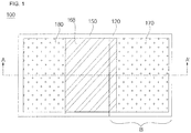
- FIG. 1 is a plan view showing a light emitting device in accordance with an embodiment
- FIG. 2 is a sectional view taken along the line A-A' of the light emitting device shown in FIG. 1 .
- the light emitting device 100 may include a support member 110 and a light emitting structure disposed on the support member 110.
- the light emitting structure may include a first semiconductor layer 120, a second semiconductor layer 140 and an active layer 130 interposed between the first semiconductor layer 120 and the second semiconductor layer 140.
- the support member 110 may be formed of a light transmittable material including, for example, any one of sapphire (Al 2 O 3 ), GaN, ZnO and AlO, although the disclosure is not limited thereto.
- a SiC support member which has a greater thermal conductivity than the sapphire (Al 2 O 3 ) support member, may be used. It is noted that the support member 110 may have an index of refraction less than that of the first semiconductor layer 120, for the sake of light extraction efficiency.
- an uneven surface pattern 112 may be formed at a lower surface of the support member 110.
- the uneven surface pattern 112 may be formed at one surface of the support member 110 opposite to the other surface where the light emitting structure is formed.
- the uneven surface pattern 112 may be formed by etching, more particularly, dry etching or wet etching, although the disclosure is not limited thereto. Such an uneven surface structure serves to prevent total reflection of light to be emitted, which may enhance light extraction efficiency.
- a buffer layer may be disposed on the support member 110, so as to relieve lattice mismatch between the support member 110 and the first semiconductor layer 120 and to enable easy growth of the first semiconductor layer 120.
- the buffer layer may be grown under a low temperature atmosphere and may be formed of a material capable of relieving a difference in a lattice constant between the first semiconductor layer 120 and the support member 110.
- the buffer layer may be formed of any one material selected from among GaN, InN, AIN, AlInN, InGaN, AlGaN and InAlGaN, although the disclosure is not limited thereto.
- the light emitting structure which includes the first semiconductor layer 120, the active layer 130 and the second semiconductor layer 140, may be formed on the buffer layer (not shown).
- the first semiconductor layer 120 may be disposed on the buffer layer (not shown).
- the first semiconductor layer 120 may be an n-type semiconductor layer and may provide the active layer 130 with electrons.
- the first semiconductor layer 120 may be formed of a semiconductor material having a composition of In x Al y Ga 1-x-y N (0 ⁇ x ⁇ 1, 0 ⁇ y ⁇ 1, 0 ⁇ x+y ⁇ 1).
- the first semiconductor layer 120 may be formed of a material selected from among GaN, AlN, AlGaN, InGaN, InN, InAlGaN, AlInN and the like.
- the first semiconductor layer 120 may be doped with an n-type dopant, such as Si, Ge, Sn and the like.
- An undoped semiconductor layer may be further provided beneath the first semiconductor layer 120, although the disclosure is not limited thereto.
- the undoped semiconductor layer (not shown) serves to enhance crystallization of the first semiconductor layer 120.
- the undoped semiconductor layer may be identical to the first semiconductor layer 120, except that it is not doped with an n-type dopant and has lower electric conductivity than the first semiconductor layer 120.
- the active layer 130 may be formed on the first semiconductor layer 120.
- the active layer 130 may be formed of a group III-V compound semiconductor material to have a single or multiple quantum well structure, a quantum wire structure, a quantum dot structure or the like.
- the active layer 130 may have a single or multiple quantum well structure including a well layer having a composition of In x Al y Ga 1 - x-y N (0 ⁇ x ⁇ 1, 0 ⁇ y ⁇ 1, 0 ⁇ x+y ⁇ 1) and a barrier layer having a composition of In a Al b Ga 1-a-b N (0 ⁇ a ⁇ 1, 0 ⁇ b ⁇ 1, 0 ⁇ a+b ⁇ 1).
- the well layer may be formed of a material having a smaller band gap than the barrier layer.
- a conductive clad layer may be formed above and/or below the active layer 130.
- the conductive clad layer may be formed of an AlGaN-based semiconductor and may have a greater band gap than the active layer 130.
- the second semiconductor layer 140 may be a p-type semiconductor layer and may provide the active layer 130 with holes.
- the second semiconductor layer 140 may be formed of a semiconductor material having a composition of In x Al y Ga 1-x-y N (0 ⁇ x ⁇ 1, 0 ⁇ y ⁇ 1, 0 ⁇ x+y ⁇ 1).
- the second semiconductor layer 140 may be formed of a material selected from among GaN, AlN, AlGaN, InGaN, InN, InAlGaN, AlInN and the like.
- the second semiconductor layer 140 may be doped with a p-type dopant, such as Mg, Zn, Ca, Sr, Ba and the like.
- An intermediate layer (not shown) may be formed between the active layer 130 and the second semiconductor layer 140.
- the intermediate layer may be an electron blocking layer, which prevents electrons, injected from the first semiconductor layer 120 into the active layer 130, from moving to the second semiconductor layer 140, rather than being recombined in the active layer 130, when high current is applied.
- the intermediate layer may have a greater band gap than the active layer 130, which may prevent electrons, injected from the first semiconductor layer 120, from being injected into the second semiconductor layer 140, rather than being recombined in the active layer 130. Accordingly, the intermediate layer may enhance electron-hole recombination possibility in the active layer 130 and may prevent current leakage.
- the above described intermediate layer may have a greater band gap than the barrier layer included in the active layer 130 and may be a semiconductor layer containing Al, such as p-type AlGaN, although the disclosure is not limited thereto.
- the first semiconductor layer 120, the active layer 130 and the second semiconductor layer 140 as described above, for example, may be formed using Metal Organic Chemical Vapor Deposition (MOCVD), Chemical Vapor Deposition (CVD), Plasma Enhanced Chemical Vapor Deposition (PECVD), Molecular Beam Epitaxy (MBE), Hydride Vapor Phase Epitaxy (HVPE), sputtering and the like, although the disclosure is not limited thereto.
- MOCVD Metal Organic Chemical Vapor Deposition
- CVD Chemical Vapor Deposition
- PECVD Plasma Enhanced Chemical Vapor Deposition
- MBE Molecular Beam Epitaxy
- HVPE Hydride Vapor Phase Epitaxy
- the conductive dopant contained in first semiconductor layer 120 and the second semiconductor layer 140 may have an even or uneven doping density.
- the plurality of semiconductor layers may be formed within a wide doping density range, although the disclosure is not limited thereto.
- the first semiconductor layer 120 may be a p-type semiconductor layer
- the second semiconductor layer 140 may be an n-type semiconductor layer
- a third semiconductor layer (not shown), which includes an n-type or p-type semiconductor layer, may be formed on the second semiconductor layer 140.
- the light emitting device 100 may have at least one among np, pn, npn and pnp junction structures.
- a light transmittable electrode layer 150 may be disposed on the second semiconductor layer 140.
- a second electrode 180 may be connected to the second semiconductor layer 140 or may be connected to the light transmittable electrode layer 150, although the disclosure is not limited thereto.
- the light transmittable electrode layer 150 may be formed of at least one selected from among ITO, IZO(In-ZnO), GZO(Ga-ZnO), AZO(Al-ZnO), AGZO(Al-Ga ZnO), IGZO(In-Ga ZnO), IrO x , RuO x , RuOx/ITO, Ni/IrO x /Au and Ni/IrO x /Au/ITO.
- the light transmittable electrode layer 150 may be formed over the entire outer surface of the second semiconductor layer 140, so as to prevent current crowding.
- the light emitting device 100 may include a first region B, which exposes a part of an upper surface of the first semiconductor layer 120 to the outside.
- the light emitting device 100 may include a first electrode 170, which is disposed on the first semiconductor layer 120 in the first region B, and a second electrode 180 which is disposed on the second semiconductor layer 140.
- An insulating layer 168 may be disposed at least between the light emitting structure and the first electrode 170.
- the first electrode 170 may be disposed on the exposed part of the upper surface of the first semiconductor layer 120 in the first region B. More particularly, at least a part of the second semiconductor layer 140 and a part of the active layer 130 are removed to expose the first semiconductor layer 120 in the first region B, and the first electrode 170 is disposed on the first semiconductor layer 120 in the first region B.
- the first electrode 170 may be spaced apart from a lateral surface of the second semiconductor layer 140 and a lateral surface of the active layer 130 by a first distance. Additionally, upper and lower surfaces of the first electrode 170 may have different areas.
- an area of an upper surface of the first electrode 170 may be in a range of 40% to 99% an area of the second semiconductor layer 140.
- the area is measured on the basis of the surface when the light emitting device 100 is viewed from the top. This will be equally applied in the following description. If the area of the first electrode 170 is 40% or less the area of the second semiconductor layer 140, bonding the light emitting device 100 in a flip chip manner to a light emitting device package may require bumps because of a small electrode area and also, may provide insufficient fixing force, which may result in deterioration in the reliability and stability of the light emitting device package upon bonding.
- placing the first electrode 170 may require removal of a great amount of the second semiconductor layer 140 and the active layer 130 of the light emitting device 100, which may result in deterioration in light emission efficiency. Accordingly, by forming the first electrode 170 as described above, both appropriate light emission efficiency and flip chip bonding stability may be accomplished.
- the first and second electrodes 170 and 180 may contain a conductive material, for example, a metal selected from among In, Co, Si, Ge, Au, Pd, Pt, Ru, Re, Mg, Zn, Hf, Ta, Rh, Ir, W, Ti, Ag, Cr, Mo, Nb, Al, Ni, Cu and WTi, or may contain alloys thereof and may be formed in a single layer or in multiple layers, although the disclosure is not limited thereto.
- a conductive material for example, a metal selected from among In, Co, Si, Ge, Au, Pd, Pt, Ru, Re, Mg, Zn, Hf, Ta, Rh, Ir, W, Ti, Ag, Cr, Mo, Nb, Al, Ni, Cu and WTi, or may contain alloys thereof and may be formed in a single layer or in multiple layers, although the disclosure is not limited thereto.
- the first distance may have a value suitable to prevent short circuit and to ensure insertion of the insulating layer, although the disclosure is not limited thereto.
- An area of the first region B may be in a range of 41% to 100% the area of the second semiconductor layer 140. In other words, when viewed from the top, the area of the first region B may be greater than the area of the first electrode 170, in order to allow the first electrode 170 to be disposed in the first region B, although the disclosure is not limited thereto.
- the second electrode 180 if an area of the second electrode 180 is excessively greater than an area of the second semiconductor layer 140, light extraction efficiency of the light emitting device 100 may be deteriorated. On the other hand, if the area of the second electrode 180 is excessively less than the area of the second semiconductor layer 140, the light emitting device 100 problematically exhibits poor reliability with respect to flip chip bonding to a light emitting device package. Accordingly, the area of the second electrode 180 may be in a range of 40% to 99% the area of the second semiconductor layer 140, although the disclosure is not limited thereto.
- the first electrode 170 or the second electrode 180 may have a tetragonal shape, a polygonal shape or a circular shape when viewed from the top, although the disclosure is not limited thereto.
- the first region B may have a tetragonal shape, a polygonal shape or a circular shape when viewed from the top, although the disclosure is not limited thereto.
- first region B and the first electrode 170 may have different shapes.
- Upper surfaces of the first electrode 170 and the second electrode 180 may be disposed on the same line. This configuration does not need bumps when the light emitting device 100 is flip chip bonded to a light emitting device package and therefore, results in saving of bump costs. Further, arranging the electrodes at the same height may enhance bonding reliability.
- the insulating layer 168 may be disposed at least between the light emitting structure and the first electrode 170.
- the insulating layer 168 may be formed at least between the first electrode 170 and the lateral surfaces of the second semiconductor layer 140 and the active layer 130. This serves to prevent short circuit of the first electrode 170 and the second semiconductor layer 140.
- the insulating layer 168 may contain a non-conductive organic material or inorganic material.
- the insulating layer 168 may be formed of urethane, polyester or acryl and may be formed in a single layer or in multiple layers, although the disclosure is not limited thereto.
- the insulating layer 168 may be formed from between the first electrode 170 and the lateral surfaces of the second semiconductor layer 140 and the active layer 130 until it reaches the same line as the upper surfaces of the first electrode 170 and the second electrode 180.
- the light emitting device 100 is free from short circuit and may achieve enhanced reliability upon flip chip bonding. Specifically, in some embodiments, it may be possible to omit bumps which have been used to adjust a difference in the height of the electrodes when a conventional light emitting device is flip chip bonded, which may enhance bonding convenience and reduce bonding time.
- FIG. 3 is a sectional view showing a light emitting device in accordance with another embodiment.
- the light emitting device 200 in accordance with the embodiment may include a support member 210 and a light emitting structure disposed on the support member 210.
- the light emitting structure may include a first semiconductor layer 220, a second semiconductor layer 240 and an active layer 230 between the first semiconductor layer 220 and the second semiconductor layer 240.
- a description of the same constituent elements as those described with reference to FIGS. 1 and 2 will be omitted hereinafter.
- a light transmittable electrode layer 250 may be disposed on the second semiconductor layer 240.
- a second electrode 280 may be connected to the second semiconductor layer 240 or may be connected to the light transmittable electrode layer 250, although the disclosure is not limited thereto.
- the light emitting device 200 may include a first region B, which exposes a part of an upper surface of the first semiconductor layer 220 to the outside.
- the light emitting device 200 may include a first electrode 270, which is disposed on the first semiconductor layer 220 in the first region B, and a second electrode 280 which is disposed on the second semiconductor layer 140.
- the first electrode 270 may be spaced apart from a lateral surface of the second semiconductor layer 240 and a lateral surface of the active layer 230 by a first distance.
- the first electrode 270 may include a lower electrode 272 connected to the first semiconductor layer 220 and an upper electrode 274 connected to one end of the lower electrode 272, the upper electrode 274 being configured to constitute an upper surface of the first electrode 270.
- the lower electrode 272 may extend at least up to a height of the second semiconductor layer 240. Also, the lower electrode 272 may be formed of the same material as that of the above described second electrode 280.
- the upper electrode 274 may be connected to one end of the lower electrode 272 so as to protrude inward of the light emitting structure.
- a partial region of the upper electrode 274 may vertically overlap with the second semiconductor layer 240 and the upper electrode 274 may be spaced apart from an upper surface of the second semiconductor layer 240.
- the first electrode 270 may have "L"-shaped cross section. That is, an upper surface of the upper electrode 274 may be a surface to be bonded to a light emitting device package, and the lower electrode 272 may serve to connect the first semiconductor layer 220 and the upper electrode 274 to each other.
- an area of the lower electrode 272 is less than an area of the upper electrode 274 by 10%, supply of electricity to the first semiconductor layer 220 may be problematic. If the area of the lower electrode 272 is greater than the area of the upper electrode 274 by 50%, the light emission efficiency of the light emitting device 200 may be deteriorated because it is necessary to etch the first region B based on the area of the lower electrode 272. Therefore, the area of the lower electrode 272 viewed from the top may be in a range of 10% to 50% the area of the upper electrode 274.
- the area of an upper surface of the first electrode 270 viewed from the top means the area of the upper electrode 274 viewed from the top.
- the area of the upper surface of the first electrode 270 viewed from the top may be in a range of 40% to 99% the area of the second semiconductor layer 240.
- FIG. 4 is a sectional view showing a configuration in which a conventional light emitting device is flip chip bonded to a package substrate
- FIG. 5 is a sectional view showing a configuration in which the light emitting device in accordance with the embodiment is flip chip bonded to a package substrate.
- a conventional light emitting device 1000 is illustrated as being flip chip bonded onto a package substrate 1390.
- Conductor patterns 1392 and 1394 are formed on the package substrate 1390.
- the conductor patterns 1392 and 1394 are electrically connected respectively to a second electrode pad 1182 and a first electrode pad 1172 of the flip chip type light emitting device 1000 via solders 1396 and 1398.
- the conventional light emitting device 1000 needs bumps due to a height difference between the second electrode pad 1182 and the first electrode pad 1172 when bonded to the package substrate 1390, which may increase bonding costs and deteriorate stability upon bonding.
- the light emitting device 100 is illustrated as being flip chip bonded onto a package substrate 190.
- Conductor patterns 192 and 194 are formed on the package substrate 190.
- the conductor patterns 192 and 194 are electrically connected respectively in a flip chip manner to the second electrode 180 and the first electrode 170.
- bonding stability may be enhanced and a vertical height of the electrode may be easily increased, which advantageously eliminates a need for separate bumps.
- the wide area electrode which exhibits effective radiation, may be suitable for a high brightness light emitting device.
- FIG. 6 is a sectional view showing a light emitting device in accordance with an alternative embodiment.
- the light emitting device 100 in accordance with the alternative embodiment has differences in that the insulating layer 168 is not provided and that the second electrode 180 penetrates the light transmittable electrode layer 150 so as to be connected to the second semiconductor layer 140.
- An empty space between the first electrode 170 and the light emitting structure may prevent short circuit of the light emitting device 100.
- the second electrode 180 may be electrically connected to the second semiconductor layer 140.
- the second electrode 180 may penetrate the light transmittable electrode layer 150 so as to be connected to the second semiconductor layer 140 and may be disposed on the light transmittable electrode layer 150, although the disclosure is not limited thereto.
- FIG. 7 is a sectional view showing a light emitting device in accordance with an alternative embodiment.
- the light emitting device 100 in accordance with the alternative embodiment has differences in the shape and height of the first electrode 170 and the second electrode 180.
- the upper surfaces of the first electrode 170 and the second electrode 180 may be disposed higher than the upper surface of the insulating layer 168 such that a spacer 199 is provided on the insulating layer 168.
- the first electrode 170 and the second electrode 180 may be disposed on different partial regions of the upper surface of the insulating layer 168.
- the spacer 199 takes the form of an empty space and may be adjusted in shape and size according to the size and height of the first electrode 170 and the second electrode 180.
- the spacer 199 may have no limit in terms of shape and size and may prevent, e.g., paste or solder from overflowing when the light emitting device 100 is attached using the paste or solder.
- FIG. 8 is a sectional view showing a light emitting device in accordance with an alternative embodiment.
- the light emitting device 200 in accordance with the alternative embodiment has a difference in that an insulating layer 268 is provided.
- the insulating layer 268 may be formed at least from between the lower electrode 272 and the lateral surfaces of the second semiconductor layer 240 and the active layer 230 to between the upper electrode 274 and the second semiconductor layer 240.
- the insulating layer 268 may contain a non-conductive organic material or inorganic material, for example, urethane, polyester or acryl, and may be formed in a single layer or in multiple layers, although the disclosure is not limited thereto.
- the insulating layer 268 may extend up to the same line as the upper surfaces of the first electrode 270 and the second electrode 280.
- the light emitting device 200 is free from short circuit and may achieve enhanced reliability upon flip chip bonding.
- FIG. 9 is a sectional view showing a light emitting device in accordance with an alternative embodiment.
- the light emitting device 100 in accordance with the alternative embodiment further includes a reflective layer 160 and has a difference in the configuration of the second electrode 180.
- the reflective layer 160 may be disposed between the light transmittable electrode layer 150 and the second electrode 180.
- the second electrode 180 may be connected to the light transmittable electrode layer 150 through an opening of the reflective layer 160. That is, the light transmittable electrode layer 150 is disposed on the second semiconductor layer 140, the reflective layer 160 is disposed on the light transmittable electrode layer 150, the second electrode 180 is disposed on the reflective layer 160, and the second electrode 180 and the light transmittable electrode layer 150 are electrically connected to each other.
- the disclosure is not limited thereto, and the second electrode 180 and the light transmittable electrode layer 150 may be connected to each other via various methods.
- the reflective layer 160 in the case in which the light emitting device 100 in accordance with the alternative embodiment is used of a flip chip type, it is possible to enhance light emission efficiency due to high reflectance of the reflective layer 160 and to ensure bonding stability and reliability due to an increased electrode area.
- the reflective layer 160 may include first layers 162 having a first index of refraction and second layers 164 having a second index of refraction that is different from the first index of refraction. That is, the reflective layer 160 may have a configuration in which the layers 162 and 164 having different indices of refraction are alternately stacked one above another.
- the first layers 162 may be layers having a low index of refraction and the second layers 164 may be layers having a high index of refraction, although the disclosure is not limited thereto.
- the reflective layer 160 takes the form of a semiconductor stack in which the first layers 162 having a low index of refraction and the second layer 164 having a high index of refraction, which have a thickness of m ⁇ /4n, are alternately stacked one above another to achieve a reflectance of 95% or more with respect to light of a particular wavelength band ⁇ .
- the first layers 162 having a low index of refraction and the second layers 164 having a high index of refraction may have a thickness of ⁇ /4 times a reference wavelength.
- the thickness of each layer 162 and 164 may be in a range of 2 ⁇ to 10 ⁇ m.
- Each layer 162 or 164 of the reflective layer 160 may be formed of M x O y or M x O y N z (M: Metal or Ceramic, O: Oxide, N: Nitride, X, Y, Z: constants).
- the first layers 162 having a low index of refraction may be formed of SiO 2 having an index of refection of 1.4 or Al 2 O 3 having an index of refection of 1.6
- the second layers 164 having a high index of refraction may be formed of TiO 2 having an index of refection of 2.0 or more, although the disclosure is not limited thereto.
- a greater reflectance may be achieved by increasing an index of refraction of a medium between the first layer 162 having a low index of refraction and the second layer 164 having a high index of refraction.
- the reflective layer 160 as described above has a greater band gap energy than an oscillation wavelength and exhibits less light absorption and consequently, greater light reflectance.
- the reflective layer 160 may extend from the upper surface of the second semiconductor layer 140 to the upper surface of the first semiconductor layer 120 along the lateral surface of the second semiconductor layer 140 and the lateral surface of the active layer 130. Accordingly, light extraction efficiency may be maximized.
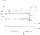
- FIG. 10 is a sectional view showing a light emitting device in accordance with an alternative embodiment.
- the light emitting device 200 in accordance with the embodiment further includes a reflective layer 260 and has a difference in the configuration of the second electrode 280.
- the reflective layer 260 is disposed between the light transmittable electrode layer 250 and the second electrode 280.
- the second electrode 280 may be connected to the light transmittable electrode layer 250 through an opening of the reflective layer 260.
- the light transmittable electrode layer 250 is disposed on the second semiconductor layer 240
- the reflective layer 260 is disposed on the light transmittable electrode layer 250
- the second electrode 280 is disposed on the reflective layer 260
- the second electrode 280 and the light transmittable electrode layer 250 are electrically connected to each other.
- the disclosure is not limited thereto, and the second electrode 280 and the light transmittable electrode layer 250 may be connected to each other via various methods.
- the reflective layer 260 in the case in which the light emitting device 200 in accordance with the alternative embodiment is used in a flip chip type, it is possible to enhance light emission efficiency due to high reflectance of the reflective layer 260 and to ensure bonding stability and reliability due to an increased electrode area.
- the configuration or material of the reflective layer 260 may be as described above.
- FIG. 11 is a sectional view showing emission of light in a configuration in which a light emitting device in accordance with an embodiment is flip chip bonded to a package substrate.
- the principle by which the light emitting device in accordance with the embodiment is flip chip bonded to achieve enhanced light extraction efficiency owing to the reflective layer 160 will be described in detail with reference to FIG. 11 .
- the light emitting device 100 is illustrated as being flip chip bonded onto the package substrate 190.
- the conductor patterns 192 and 194 are formed on the package substrate 190 and are electrically connected to the second electrode 180 and the first electrode 170.
- the wide area electrode which exhibits effective radiation, may be suitable for a high brightness light emitting device.
- the reflective layer 160 formed as described above serves not only to protect the light transmittable electrode layer 150 or the first semiconductor layer 120, but also to prevent light absorption and allow light to be directed to the support member 110, thereby enhancing light extraction efficiency of the light emitting device 100.
- the light emitted from the active layer 130 is reflected by the reflective layer 160 to thereby be wholly directed to the support member 110, which may enhance light emission efficiency of the flip chip type light emitting device 100.
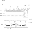
- FIG. 12 is a bottom view showing a light emitting device in accordance with an alternative embodiment
- FIG. 13 is a sectional view of the light emitting device shown in FIG. 12 .
- the light emitting device 300 in accordance with the alternative embodiment includes a support member 310 having a cavity c and the cavity c is filled with a sealing material 314 containing a fluorescent substance 316.
- the cavity c may have various shapes so long as it defines a predetermined space therein and for example, may have a tetragonal, polygonal or circular shape when viewed from the top.
- the cross section of the cavity c may have a cup shape, a concave container shape or the like, and an inner lateral surface of the cavity c may be perpendicular to or inclined from a bottom surface of the cavity c.
- the cavity c may have a circular shape, a tetragonal shape, a polygonal shape, an elliptical shape or the like when viewed from the front, although the disclosure is not limited thereto.
- the front shape of the cavity c may be freely selected.
- the depth h of the cavity c may be in a range of 0.3 to 0.7 times a thickness of the support member 310, although the disclosure is not limited thereto.
- the cavity c may deteriorate rigidity of the support member 310. If the cavity c has an excessively small length L1, it does not provide a sufficient space for white light excitation of light emitted from the active layer 330 and causes deterioration in color rendering because light may be directed to a place where the cavity c is not present. Therefore, the length L1 of the cavity c may be in a range of 0.8 to 0.95 times a length of the support member 310, although the disclosure is not limited thereto.
- the cavity c may deteriorate rigidity of the support member 310. If the cavity c has an excessively small width L2, it does not provide a sufficient space for white light excitation of light emitted from the active layer 330 and causes deterioration in color rendering because light may be directed to a place where the cavity c is not present. Therefore, the width L2 of the cavity c may be in a range of 0.8 to 0.95 times the length of the support member 310, although the disclosure is not limited thereto.
- the cavity c may be opened in the bottom of the support member 310 and may contain the sealing material 314. That is, the cavity c may be filled with and sealed by the sealing material 314.
- the length of the light emitting device 300 may be in a range of 6 to 12 times the thickness of the light emitting device 300, although the disclosure is not limited thereto.
- the sealing material 314 may be a light transmittable resin material, such as silicon or epoxy. After the material is filled in the cavity c, the material may be subjected to ultraviolet or thermal curing, although the disclosure is not limited thereto.
- the sealing material 314 may contain the fluorescent substance 316.
- the kind of the fluorescent substance 316 is selected according to the wavelength of light emitted from the active layer 330, so as to allow the light emitting device 300 to emit white light. Accordingly, the fluorescent substance 316 may include at least one selected from among, for example, red, blue and yellow fluorescent substances, and may include various kinds of fluorescent substances, although the disclosure is not limited thereto.
- the fluorescent substance may be excited by light having a first color that is emitted from the active layer 330 to thereby generate light having a second color.
- the light emitted from the active layer 330 is blue light and the fluorescent substance is a yellow fluorescent substance
- the yellow fluorescent substance may emit white light by being excited by the blue light.
- the light emitted from the active layer 330 is green light
- use of a magenta fluorescent substance or a mixture of blue and red fluorescent substances may be exemplified
- use of a cyan fluorescent substance or a mixture of blue and green fluorescent substances may be exemplified.
- the fluorescent substance 316 may be a known fluorescent substance, such as a YAG-based, TAG-based, sulfide-based, silicate-based, aluminate-based, nitride-based, carbide-based, nitridosilicate-based, borate-based, fluoride-based, phosphate-based fluorescent substance or the like.
- the sealing material 314 may further contain a light diffuser to diffuse light emitted from the active layer 330.
- the light diffuser may be any one of white metal oxides, such as titanium dioxide (TiO 2 ), barium oxide (BaO), silicon dioxide (SiO 2 ), magnesium oxide (MgO) and yttrium oxide (Y 2 O 3 ), or may be a mixture of at least two selected from among titanium dioxide (TiO 2 ), barium oxide (BaO), silicon dioxide (SiO 2 ), magnesium oxide (MgO) and yttrium oxide (Y 2 O 3 ).
- a light diffuser Through use of the light diffuser, irregular reflection of light emitted from the light emitting device may be induced.
- FIG. 14 is a sectional view showing a light emitting device in accordance with an alternative embodiment.
- the light emitting device 300 in accordance with the alternative embodiment has a difference in that the support member 310 has a plurality of cavities c.
- the support member 310 has a plurality of cavities c.
- the cavity c is not limited to a specific number and may be prepared in various numbers according to the size and kind of the light emitting device 300 and the kind of light to be emitted.
- a distance between neighboring cavities may be less than a length of the cavity c, although the disclosure is not limited thereto.
- a difference in the index of refraction between a region having the cavities c and a region having no cavities causes irregular reflection, which may result in enhanced light emission efficiency and color rendering of the light emitting device 300.
- the cavity c may have various shapes so long as it defines a predetermined space therein and for example, may have a tetragonal shape, a polygonal shape or a circular shape when viewed from the top.
- the cross section of the cavity c may have a cup shape, a concave container shape or the like, and an inner lateral surface of the cavity c may be perpendicular to or inclined from a bottom surface of the cavity c.
- the cavity c may have a circular shape, a tetragonal shape, a polygonal shape, an elliptical shape or the like when viewed from the front, although the disclosure is not limited thereto.
- the front shape of the cavity c may be freely selected.
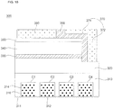
- FIG. 15 is a sectional view showing a light emitting device in accordance with an alternative embodiment
- FIG. 16 is a sectional view showing a light emitting device in accordance with an alternative embodiment.
- the light emitting device 300 in accordance with the alternative embodiment is configured in such a way that uneven patterns 311 and 312 may be formed at a lower surface of the support member 310 or the cavity c.
- the uneven patterns 311 and 312 may be an arrangement of a plurality of semi-spheres, cones and cylinders, which may be arranged regularly or irregularly.
- the uneven patterns 311 and 312 may be formed by etching, more particularly, dry etching or wet etching, although the disclosure is not limited thereto.
- the uneven patterns 311 and 312 serve to induce irregular reflection of light emitted from the active layer 330, thereby enhancing color rendering of the light emitting device 300 and achieving enhanced light extraction efficiency by preventing total reflection of light.
- the light emitting device 300 in accordance with the alternative embodiment is configured in such a way that uneven patterns 311 and 312 may be formed at a lower surface of the support member 310 or the cavity c.
- the uneven patterns 311 and 312 are those as described in FIG. 3 .
- the uneven patterns 311 and 312 induce irregular reflection of light emitted from the active layer 330, thereby enhancing color rendering of the light emitting device 300 and achieving enhanced light extraction efficiency by preventing total reflection of light. Additionally, the uneven patterns 311 and 312 may enhance light emission efficiency,
- FIG. 17 is a sectional view showing a light emitting device in accordance with an alternative embodiment.
- the light emitting device 300 in accordance with the alternative embodiment has a difference in the shape of a lateral surface of the cavity c. Specifically, the length of the cavity c may increase with decreasing distance to a lower surface of the first semiconductor layer 320.
- the length of the cavity c may increase with decreasing distance to the lower surface of the first semiconductor layer 320, thereby providing the cavity c with an inverted trapezoidal cross section.
- the lateral surface of the cavity c is illustrated as having a linear shape, it may have a curvilinear shape or curved surface shape or may be stepped. However, the disclosure is not limited thereto.
- the cavity c Through use of the cavity c, it may be possible to prevent the sealing material 314 from being separated from the support member 310. Also, increasing the length of the cavity c with decreasing distance to the active layer 330 is advantageous to realize white light, and reducing the length of the cavity c at the bottom of the support member 310 may minimize deterioration in the rigidity of the support member 310.
- FIG. 18 is a sectional view showing a light emitting device in accordance with an alternative embodiment.
- the light emitting device 300 in accordance with the embodiment has a difference in the shape of the lateral surface of the cavity c. Specifically, the lateral surface of the cavity c may be stepped.
- the length of the cavity c increases with decreasing distance to the lower surface of the first semiconductor layer 320 and the lateral surface of the cavity c may be stepped.
- the number of steps is not limited and may be determined according to the size and kind of the light emitting device. Also, the steps may have a curvilinear shape or curved surface shape, although the disclosure is not limited thereto.
- the cavity c Through use of the cavity c, it may be possible to prevent the sealing material 314 from being separated from the support member 310. Also, increasing the length of the cavity c with decreasing distance to the active layer 330 is advantageous to realize white light, and reducing the length of the cavity c at the bottom of the support member 310 may minimize deterioration in the rigidity of the support member 310. Moreover, providing the cavity c with the stepped lateral surface may further prevent separation of the sealing material 314 from the support member 310.
- FIG. 19 is a sectional view showing a light emitting device in accordance with an alternative embodiment.
- the light emitting device 300 in accordance with the embodiment has a difference in that the sealing material 314 may include a first sealing material 314a stacked on the bottom of the cavity c and a second sealing material 314b stacked on the first sealing material 314a.
- the first sealing material 314a may contain a light diffuser 318 to diffuse light to be emitted from the light emitting device 300. Both the first sealing material 314a and the second sealing material 314b may contain the fluorescent substance 316. Through use of the light diffuser 318, it may be possible to further enhance color rendering of light emitted from the active layer 330.
- FIG. 20 is a sectional view showing a light emitting device in accordance with an alternative embodiment.
- the light emitting device 300 in accordance with the embodiment may have a difference in that a lower surface of the sealing material 314 may be centrally concave.
- the sealing material 314 may act as a lens to reduce an irradiation angle of light emitted from the active layer 330, which may enhance concentration of the light.
- FIG. 21 is a sectional view showing a light emitting device in accordance with an alternative embodiment.
- the light emitting device 300 in accordance with the alternative embodiment has a difference in that the lower surface of the sealing material 314 may be centrally convex.
- the sealing material 314 may act as a lens to increase an irradiation angle of light emitted from the active layer 330, which may enhance diffusion of the light.
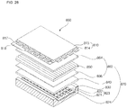
- FIG. 22 is a sectional view of a light emitting device package including a light emitting device in accordance with an embodiment.
- the light emitting device package 500 in accordance with the embodiment may include a body 531, a first electrode layer 538 and a second electrode layer 539 mounted on the body 531, and a light emitting device 536 mounted on the body 531 and electrically connected to the first electrode layer 538 and the second electrode layer 539.
- the light emitting device 536 may be connected in a flip chip manner to the first electrode layer 538 and the second electrode layer 539.
- the body 531 may be formed of a silicon material, a synthetic resin material or a metal material, and the light emitting device 536 may be surrounded by an inclined surface.
- the first electrode layer 538 and the second electrode layer 539 are electrically separated from each other and serve to supply power to the light emitting device 536.
- the first electrode layer 538 and the second electrode layer 539 may serve not only to reflect light emitted from the light emitting device 536, thereby increasing light emission efficiency, but also to discharge heat generated from the light emitting device 536 to the outside.
- a reflective layer 532 may be formed on the body 531, to more effectively concentrate light emitted from the light emitting device 536 forward.
- the reflective layer 532 may be formed of a metal having a high coefficient of reflection, such as silver (Ag), aluminum (Al) and the like.
- an insulating layer 533 may further be formed on the reflective layer 532.
- a cavity 537 is formed in the body 531 such that the light emitting diode 536 is bonded in the cavity 537.
- the cavity 537 may be filled with a molding member to enclose and protect the light emitting diode 536.
- the molding member may contain a fluorescent substance to change a wavelength of light emitted from the light emitting device 536.
- the electrode layers Accordingly, owing to a wide area of the electrode layers, it may be possible to enhance bonding stability and reliability of the light emitting device 536 and to minimize deterioration in the light emission efficiency of the light emitting device 536. Further, the light emitting device 536 may be directly bonded using paste without bumps.
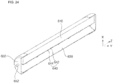
- FIG. 23 is a perspective view showing a lighting apparatus including a light emitting device package in accordance with an embodiment
- FIG. 24 is a sectional view taken along the line C-C' of the lighting apparatus shown in FIG. 23 .
- the lighting apparatus 600 may include a body 610, a cover 630 coupled to the body 610, and end caps 650 disposed at opposite ends of the body 610.
- a light emitting device module 640 may be coupled to a lower surface of the body 610.
- the body 610 may be formed of a metal material having excellent conductivity and heat radiation effects, to discharge heat generated in light emitting device packages 644 to the outside through an upper surface of the body 610.
- the light emitting device packages 644 may have multiple colors and may be arranged in multiple rows on a printed circuit board 642 to form an array. Also, the light emitting device packages 644 may be arranged by the same distance or by different distances as occasion demands, to enable adjustment of brightness.
- the printed circuit board 642 may be formed of a Metal Core PCB (MCPCB), FR4 PCB or the like.
- the light emitting device packages 644 may include a lead frame (not shown) to have an enhanced radiation function. Therefore, the reliability and efficiency of the light emitting device packages 644 may be enhanced, and the lifespan of the lighting apparatus 600 including the light emitting device packages 644 as well as the lifespan of the light emitting device packages 644 may be extended.
- the cover 630 may have a circular shape to surround the lower surface of the body 610, although the disclosure is not limited thereto.
- the cover 630 protects the light emitting device module 640 from external foreign substances, etc.
- the cover 630 may contain diffusive particles to prevent glare of light emitted from the light emitting device packages 644 and to ensure uniform emission of light to the outside.
- a prism pattern may be formed on at least one of an inner surface and an outer surface of the cover 630.
- a fluorescent substance may be applied to at least one of the inner surface and the outer surface of the cover 630.
- the cover 630 must have not only excellent light transmittance, but also heat resistance sufficient to endure heat generated from the light emitting device packages 644.
- the cover 630 may be formed of Polyethylene Terephthalate (PET), Polycarbonate (PC), PolymethylMethacrylate (PMMA) or the like.
- the end caps 650 may be disposed at opposite ends of the body 610 and serve to hermetically seal a power device (not shown).
- the end caps 650 may be provided with power pins 652, which allows the lighting apparatus 600 in accordance with the embodiment to be directly used in a terminal, from which an existing fluorescent lamp has been removed, without requiring a separate device.
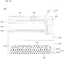
- FIG. 25 is an exploded perspective view of a liquid crystal display apparatus including a light emitting device in accordance with an embodiment.
- FIG. 25 illustrates an edge light type liquid crystal display apparatus 700, which may include a liquid crystal display panel 710 and a backlight unit 770 to irradiate light to the liquid crystal display panel 710.
- the liquid crystal display panel 710 may display an image using light generated from the backlight unit 770.
- the liquid crystal display panel 710 may include a color filter substrate 712 and a thin film transistor substrate 714, which are arranged to face each other with liquid crystals interposed therebetween.
- the color filter substrate 312 may realize the color of the image displayed via the liquid crystal display panel 710.
- the thin film transistor substrate 714 is electrically connected to a printed circuit board 718, on which a plurality of circuit elements is mounted, by means of a drive film 717.
- the thin film transistor substrate 714 may apply drive voltage, provided by the printed circuit board 718, to the liquid crystals in response to a drive signal transmitted from the printed circuit board 718.
- the thin film transistor substrate 714 may include pixel electrodes and thin film transistors in the form of thin films formed on another substrate formed of a transparent material, such as glass, plastic or the like.
- the backlight unit 770 includes a light emitting device module 720 to emit light, a light guide plate 730 to change light emitted from the light emitting device module 720 into planar light and transmit the planar light to the liquid crystal display panel 710, a plurality of films 750, 760 and 764 to achieve uniformity in brightness distribution and improve vertical light incidence of the light having passed through the light guide plate 730, and a reflective sheet 740 to reflect light, emitted rearward from the light guide plate 730, toward the light guide plate 730.
- the light emitting device module 720 may include a plurality of light emitting device packages 724 and a printed circuit board 722 on which the plurality of light emitting device packages 724 is mounted to define an array.
- the backlight unit 770 may include a diffusive film 766, which diffuses incident light from the liquid guide plate 730 toward the liquid display panel 710, and a prism film 750 which condenses the diffused light to enhance vertical incidence.
- the prism film 750 may include a protective film 764 to protect the prism film 750.
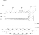
- FIG. 26 is an exploded perspective view of a liquid crystal display apparatus including a light emitting device in accordance with an embodiment. The same configuration as that illustrated and described in FIG. 25 will not be repeated hereinafter.
- FIG. 26 illustrates a vertical type liquid crystal display apparatus 800, which may include a liquid crystal display panel 810 and a backlight unit 870 to irradiate light to the liquid crystal display panel 810.
- the liquid crystal display panel 810 is identical to the description with reference to FIG. 25 and thus, a detailed description thereof will be omitted.
- the backlight unit 870 may include a plurality of light emitting device modules 823, a reflective sheet 824, a lower chassis 830 in which the light emitting device modules 823 and the reflective sheet 824 are accommodated, a diffusive plate 840 and a plurality of optical films 860 disposed above the light emitting device modules 823.
- Each of the light emitting device modules 823 may include a plurality of light emitting device packages 822 and a printed circuit board 821 on which the plurality of light emitting device packages 822 is mounted to form an array.
- the reflective sheet 824 serves to reflect light emitted from the light emitting device packages 822 toward the liquid crystal display panel 810, thereby improving use efficiency of the light.
- the light emitted from the light emitting device modules 823 is introduced into the diffusive plate 840, and optical films 860 are disposed above the diffusive plate 840.
- the optical films 860 may include a diffusive film 866, a prism film 850 and a protective film 864.
- the embodiments provide a flip chip type light emitting device, which achieves enhanced light emission efficiency as well as stability and reliability upon bonding to a light emitting device package.
- the flip chip type light emitting device does not need separate bumps upon bonding, which may result in reduction in production costs and time.
Description
- Embodiments relate to a light emitting device, which is of a flip chip type with enhanced light emission efficiency and exhibits stability and reliability upon bonding to a light emitting device package.
- Light Emitting Diodes (LEDs) are a representative example of light emitting devices, which convert electric signals into infrared light or visible light using characteristics of compound semiconductors. Such LEDs are being utilized in home appliances, remote controllers, electronic bulletin boards, displays and various other automated machines. The application range of LEDs is gradually increasing.
- Exemplary LEDs mounted in flip chip configurations are disclosed in
US 2006/0169994 A1 andUS 2011/0233588 A1 . - Generally, miniature LEDs are fabricated into surface mount devices so as to be directly mounted on a Printed Circuit Board (PCB) and hence, an LED lamp, which serves as a display device, is being developed into a surface mount device. The surface mount device can substitute for a conventional simple lamp and is used in a variety of color on-and-off displays and letter/image displays.
- The increased application range of LEDs causes a demand for higher brightness of household lights as well as emergency lights and therefore, it is important to enhance brightness of LEDs.
- Embodiments provide a light emitting device, which is of a flip chip type with enhanced light emission efficiency and exhibits stability and reliability upon bonding to a light emitting device package.
- A light emitting device according to the current invention is as defined in claim 1. Embodiments are further defined in claims 2-11 There is also provided a light emitting device package as defined in claim 12.
- Details of the embodiments will be more clearly understood from the following detailed description taken in conjunction with the accompanying drawings. In the description, any reference to "embodiment(s)" or "aspect(s) of the invention" not falling under the scope of the claims should be interpreted as illustrative examples for understanding the invention. In the drawings:
-
FIG. 1 is a plan view showing a light emitting device in accordance with an embodiment; -
FIG. 2 is a sectional view taken along the line A-A' of the light emitting device shown inFIG. 1 ; -
FIG. 3 is a sectional view showing a light emitting device in accordance with another embodiment; -
FIG. 4 is a sectional view showing a configuration in which a conventional light emitting device is flip chip bonded to a package substrate; -
FIG. 5 is a sectional view showing a configuration in which the light emitting device in accordance with the embodiment is flip chip bonded to a package substrate; -
FIG. 6 is a sectional view showing a light emitting device in accordance with an alternative embodiment; -
FIG. 7 is a sectional view showing a light emitting device in accordance with an alternative embodiment; -
FIG. 8 is a sectional view showing a light emitting device in accordance with an alternative embodiment; -
FIG. 9 is a sectional view showing a light emitting device in accordance with an alternative embodiment; -
FIG. 10 is a sectional view showing a light emitting device in accordance with an alternative embodiment; -
FIG. 11 is a view explaining emission of light in a configuration in which a light emitting device in accordance with an embodiment is flip chip bonded to a package substrate; -
FIG. 12 is a bottom view showing a light emitting device in accordance with an alternative embodiment; -
FIG. 13 is a sectional view of the light emitting device shown inFIG. 12 ; -
FIG. 14 is a sectional view showing a light emitting device in accordance with an alternative embodiment; -
FIG. 15 is a sectional view showing a light emitting device in accordance with an alternative embodiment; -
FIG. 16 is a sectional view showing a light emitting device in accordance with an alternative embodiment; -
FIG. 17 is a sectional view showing a light emitting device in accordance with an alternative embodiment; -
FIG. 18 is a sectional view showing a light emitting device in accordance with an alternative embodiment; -
FIG. 19 is a sectional view showing a light emitting device in accordance with an alternative embodiment; -
FIG. 20 is a sectional view showing a light emitting device in accordance with an alternative embodiment; -
FIG. 21 is a sectional view showing a light emitting device in accordance with an alternative embodiment; -
FIG. 22 is a sectional view of a light emitting device package including a light emitting device in accordance with an embodiment; -
FIG. 23 is a perspective view showing a lighting apparatus including a light emitting device package in accordance with an embodiment; -
FIG. 24 is a sectional view taken along the line C-C' of the lighting apparatus shown inFIG. 23 ; -
FIG. 25 is an exploded perspective view of a liquid crystal display apparatus including a light emitting device in accordance with an embodiment; and -
FIG. 26 is an exploded perspective view of a liquid crystal display apparatus including a light emitting device in accordance with an embodiment. - Reference will now be made in detail to embodiments, examples of which are illustrated in the accompanying drawings. However, the present disclosure may be embodied in many different forms and should not be construed as limited to the embodiments set forth herein. Rather, these embodiments are provided so that this disclosure will be thorough and complete, and will fully convey the scope of the disclosure to those skilled in the art. The present disclosure is defined only by the categories of the claims. In certain embodiments, detailed descriptions of device constructions or processes well known in the art may be omitted to avoid obscuring appreciation of the disclosure by a person of ordinary skill in the art. Wherever possible, the same reference numbers will be used throughout the drawings to refer to the same or like parts.
- Spatially-relative terms such as "below", "beneath", "lower", "above", or "upper" may be used herein to describe one element's relationship to another element as illustrated in the Figures. It will be understood that spatially-relative terms are intended to encompass different orientations of the device in addition to the orientation depicted in the Figures. For example, if the device in one of the figures is turned over, elements described as "below" or "beneath" other elements would then be oriented "above" the other elements. The exemplary terms "below" or "beneath" can, therefore, encompass both an orientation of above and below. Since the device may be oriented in another direction, the spatially-relative terms may be interpreted in accordance with the orientation of the device.
- The terminology used in the present disclosure is for the purpose of describing particular embodiments only and is not intended to limit the disclosure. As used in the disclosure and the appended claims, the singular forms "a", "an" and "the" are intended to include the plural forms as well, unless context clearly indicates otherwise. It will be further understood that the terms "comprises" and/or "comprising," when used in this specification, specify the presence of stated features, integers, steps, operations, elements, and/or components, but do not preclude the presence or addition of one or more other features, integers, steps, operations, elements, components, and/or groups thereof.
- Unless otherwise defined, all terms (including technical and scientific terms) used herein have the same meaning as commonly understood by one of ordinary skill in the art. It will be further understood that terms, such as those defined in commonly used dictionaries, should be interpreted as having a meaning that is consistent with their meaning in the context of the relevant art and the present disclosure, and will not be interpreted in an idealized or overly formal sense unless expressly so defined herein.
- In the drawings, the thickness or size of each layer is exaggerated, omitted, or schematically illustrated for convenience of description and clarity. Also, the size or area of each constituent element does not entirely reflect the actual size thereof.
- Angles or directions used to describe the structures of light emitting devices according to embodiments are based on those shown in the drawings. Unless there is, in the specification, no definition of a reference point to describe angular positional relations in the structures of the light emitting devices, the associated drawings may be referred to.
-
FIG. 1 is a plan view showing a light emitting device in accordance with an embodiment, andFIG. 2 is a sectional view taken along the line A-A' of the light emitting device shown inFIG. 1 . - Referring to
FIGS. 1 and2 , thelight emitting device 100 may include asupport member 110 and a light emitting structure disposed on thesupport member 110. The light emitting structure may include afirst semiconductor layer 120, asecond semiconductor layer 140 and anactive layer 130 interposed between thefirst semiconductor layer 120 and thesecond semiconductor layer 140. - The
support member 110 may be formed of a light transmittable material including, for example, any one of sapphire (Al2O3), GaN, ZnO and AlO, although the disclosure is not limited thereto. Alternatively, a SiC support member, which has a greater thermal conductivity than the sapphire (Al2O3) support member, may be used. It is noted that thesupport member 110 may have an index of refraction less than that of thefirst semiconductor layer 120, for the sake of light extraction efficiency. - To further enhance light extraction efficiency, an
uneven surface pattern 112 may be formed at a lower surface of thesupport member 110. - The
uneven surface pattern 112 may be formed at one surface of thesupport member 110 opposite to the other surface where the light emitting structure is formed. Theuneven surface pattern 112 may be formed by etching, more particularly, dry etching or wet etching, although the disclosure is not limited thereto. Such an uneven surface structure serves to prevent total reflection of light to be emitted, which may enhance light extraction efficiency. - A buffer layer (not shown) may be disposed on the
support member 110, so as to relieve lattice mismatch between thesupport member 110 and thefirst semiconductor layer 120 and to enable easy growth of thefirst semiconductor layer 120. The buffer layer (not shown) may be grown under a low temperature atmosphere and may be formed of a material capable of relieving a difference in a lattice constant between thefirst semiconductor layer 120 and thesupport member 110. For example, the buffer layer (not shown) may be formed of any one material selected from among GaN, InN, AIN, AlInN, InGaN, AlGaN and InAlGaN, although the disclosure is not limited thereto. - The light emitting structure, which includes the
first semiconductor layer 120, theactive layer 130 and thesecond semiconductor layer 140, may be formed on the buffer layer (not shown). - The
first semiconductor layer 120 may be disposed on the buffer layer (not shown). Thefirst semiconductor layer 120 may be an n-type semiconductor layer and may provide theactive layer 130 with electrons. In one example, thefirst semiconductor layer 120 may be formed of a semiconductor material having a composition of InxAlyGa1-x-yN (0≤x≤1, 0≤y≤1, 0≤x+y≤1). For example, thefirst semiconductor layer 120 may be formed of a material selected from among GaN, AlN, AlGaN, InGaN, InN, InAlGaN, AlInN and the like. Additionally, thefirst semiconductor layer 120 may be doped with an n-type dopant, such as Si, Ge, Sn and the like. - An undoped semiconductor layer (not shown) may be further provided beneath the
first semiconductor layer 120, although the disclosure is not limited thereto. The undoped semiconductor layer (not shown) serves to enhance crystallization of thefirst semiconductor layer 120. The undoped semiconductor layer may be identical to thefirst semiconductor layer 120, except that it is not doped with an n-type dopant and has lower electric conductivity than thefirst semiconductor layer 120. - The
active layer 130 may be formed on thefirst semiconductor layer 120. Theactive layer 130 may be formed of a group III-V compound semiconductor material to have a single or multiple quantum well structure, a quantum wire structure, a quantum dot structure or the like. - In the case in which the
active layer 130 has a quantum well structure, for example, theactive layer 130 may have a single or multiple quantum well structure including a well layer having a composition of InxAlyGa1-x-yN (0≤x≤1, 0≤y≤1, 0≤x+y≤1) and a barrier layer having a composition of InaAlbGa1-a-bN (0≤a≤1, 0≤b≤1, 0≤a+b≤1). The well layer may be formed of a material having a smaller band gap than the barrier layer. - A conductive clad layer (not shown) may be formed above and/or below the
active layer 130. The conductive clad layer (not shown) may be formed of an AlGaN-based semiconductor and may have a greater band gap than theactive layer 130. - The
second semiconductor layer 140 may be a p-type semiconductor layer and may provide theactive layer 130 with holes. In one example, thesecond semiconductor layer 140 may be formed of a semiconductor material having a composition of InxAlyGa1-x-yN (0≤x≤1, 0≤y≤1, 0≤x+y≤1). For example, thesecond semiconductor layer 140 may be formed of a material selected from among GaN, AlN, AlGaN, InGaN, InN, InAlGaN, AlInN and the like. Additionally, thesecond semiconductor layer 140 may be doped with a p-type dopant, such as Mg, Zn, Ca, Sr, Ba and the like. - An intermediate layer (not shown) may be formed between the
active layer 130 and thesecond semiconductor layer 140. The intermediate layer may be an electron blocking layer, which prevents electrons, injected from thefirst semiconductor layer 120 into theactive layer 130, from moving to thesecond semiconductor layer 140, rather than being recombined in theactive layer 130, when high current is applied. The intermediate layer may have a greater band gap than theactive layer 130, which may prevent electrons, injected from thefirst semiconductor layer 120, from being injected into thesecond semiconductor layer 140, rather than being recombined in theactive layer 130. Accordingly, the intermediate layer may enhance electron-hole recombination possibility in theactive layer 130 and may prevent current leakage. - The above described intermediate layer may have a greater band gap than the barrier layer included in the
active layer 130 and may be a semiconductor layer containing Al, such as p-type AlGaN, although the disclosure is not limited thereto. - The
first semiconductor layer 120, theactive layer 130 and thesecond semiconductor layer 140 as described above, for example, may be formed using Metal Organic Chemical Vapor Deposition (MOCVD), Chemical Vapor Deposition (CVD), Plasma Enhanced Chemical Vapor Deposition (PECVD), Molecular Beam Epitaxy (MBE), Hydride Vapor Phase Epitaxy (HVPE), sputtering and the like, although the disclosure is not limited thereto. - The conductive dopant contained in
first semiconductor layer 120 and thesecond semiconductor layer 140 may have an even or uneven doping density. In other words, the plurality of semiconductor layers may be formed within a wide doping density range, although the disclosure is not limited thereto. - Alternatively, the
first semiconductor layer 120 may be a p-type semiconductor layer, thesecond semiconductor layer 140 may be an n-type semiconductor layer, and a third semiconductor layer (not shown), which includes an n-type or p-type semiconductor layer, may be formed on thesecond semiconductor layer 140. Accordingly, thelight emitting device 100 may have at least one among np, pn, npn and pnp junction structures. - A light
transmittable electrode layer 150 may be disposed on thesecond semiconductor layer 140. In this case, asecond electrode 180 may be connected to thesecond semiconductor layer 140 or may be connected to the lighttransmittable electrode layer 150, although the disclosure is not limited thereto. - The light
transmittable electrode layer 150 may be formed of at least one selected from among ITO, IZO(In-ZnO), GZO(Ga-ZnO), AZO(Al-ZnO), AGZO(Al-Ga ZnO), IGZO(In-Ga ZnO), IrOx, RuOx, RuOx/ITO, Ni/IrOx/Au and Ni/IrOx/Au/ITO. The lighttransmittable electrode layer 150 may be formed over the entire outer surface of thesecond semiconductor layer 140, so as to prevent current crowding. - The
light emitting device 100 may include a first region B, which exposes a part of an upper surface of thefirst semiconductor layer 120 to the outside. Thelight emitting device 100 may include afirst electrode 170, which is disposed on thefirst semiconductor layer 120 in the first region B, and asecond electrode 180 which is disposed on thesecond semiconductor layer 140. An insulatinglayer 168 may be disposed at least between the light emitting structure and thefirst electrode 170. Thefirst electrode 170 may be disposed on the exposed part of the upper surface of thefirst semiconductor layer 120 in the first region B. More particularly, at least a part of thesecond semiconductor layer 140 and a part of theactive layer 130 are removed to expose thefirst semiconductor layer 120 in the first region B, and thefirst electrode 170 is disposed on thefirst semiconductor layer 120 in the first region B. - The
first electrode 170 may be spaced apart from a lateral surface of thesecond semiconductor layer 140 and a lateral surface of theactive layer 130 by a first distance. Additionally, upper and lower surfaces of thefirst electrode 170 may have different areas. - When viewed from the top, an area of an upper surface of the
first electrode 170 may be in a range of 40% to 99% an area of thesecond semiconductor layer 140. Here, the area is measured on the basis of the surface when thelight emitting device 100 is viewed from the top. This will be equally applied in the following description. If the area of thefirst electrode 170 is 40% or less the area of thesecond semiconductor layer 140, bonding thelight emitting device 100 in a flip chip manner to a light emitting device package may require bumps because of a small electrode area and also, may provide insufficient fixing force, which may result in deterioration in the reliability and stability of the light emitting device package upon bonding. If the area of thefirst electrode 170 is 99% or more the area of thesecond semiconductor layer 140, placing thefirst electrode 170 may require removal of a great amount of thesecond semiconductor layer 140 and theactive layer 130 of thelight emitting device 100, which may result in deterioration in light emission efficiency. Accordingly, by forming thefirst electrode 170 as described above, both appropriate light emission efficiency and flip chip bonding stability may be accomplished. - The first and
second electrodes - The first distance may have a value suitable to prevent short circuit and to ensure insertion of the insulating layer, although the disclosure is not limited thereto.
- An area of the first region B may be in a range of 41% to 100% the area of the
second semiconductor layer 140. In other words, when viewed from the top, the area of the first region B may be greater than the area of thefirst electrode 170, in order to allow thefirst electrode 170 to be disposed in the first region B, although the disclosure is not limited thereto. - With regard to the
second electrode 180, if an area of thesecond electrode 180 is excessively greater than an area of thesecond semiconductor layer 140, light extraction efficiency of thelight emitting device 100 may be deteriorated. On the other hand, if the area of thesecond electrode 180 is excessively less than the area of thesecond semiconductor layer 140, thelight emitting device 100 problematically exhibits poor reliability with respect to flip chip bonding to a light emitting device package. Accordingly, the area of thesecond electrode 180 may be in a range of 40% to 99% the area of thesecond semiconductor layer 140, although the disclosure is not limited thereto. - The
first electrode 170 or thesecond electrode 180 may have a tetragonal shape, a polygonal shape or a circular shape when viewed from the top, although the disclosure is not limited thereto. - In this case, the first region B may have a tetragonal shape, a polygonal shape or a circular shape when viewed from the top, although the disclosure is not limited thereto.
- Although it is desirable that the first region B and the
first electrode 170 have the same shape when viewed from the top, the first region B and thefirst electrode 170 may have different shapes. - Upper surfaces of the
first electrode 170 and thesecond electrode 180 may be disposed on the same line. This configuration does not need bumps when thelight emitting device 100 is flip chip bonded to a light emitting device package and therefore, results in saving of bump costs. Further, arranging the electrodes at the same height may enhance bonding reliability. - The insulating
layer 168 may be disposed at least between the light emitting structure and thefirst electrode 170. The insulatinglayer 168 may be formed at least between thefirst electrode 170 and the lateral surfaces of thesecond semiconductor layer 140 and theactive layer 130. This serves to prevent short circuit of thefirst electrode 170 and thesecond semiconductor layer 140. The insulatinglayer 168 may contain a non-conductive organic material or inorganic material. In one example, the insulatinglayer 168 may be formed of urethane, polyester or acryl and may be formed in a single layer or in multiple layers, although the disclosure is not limited thereto. - To further prevent short circuit, the insulating
layer 168 may be formed from between thefirst electrode 170 and the lateral surfaces of thesecond semiconductor layer 140 and theactive layer 130 until it reaches the same line as the upper surfaces of thefirst electrode 170 and thesecond electrode 180. - Through provision of the insulating
layer 168, thelight emitting device 100 is free from short circuit and may achieve enhanced reliability upon flip chip bonding. Specifically, in some embodiments, it may be possible to omit bumps which have been used to adjust a difference in the height of the electrodes when a conventional light emitting device is flip chip bonded, which may enhance bonding convenience and reduce bonding time. -
FIG. 3 is a sectional view showing a light emitting device in accordance with another embodiment. - Referring to
FIG. 3 , thelight emitting device 200 in accordance with the embodiment may include asupport member 210 and a light emitting structure disposed on thesupport member 210. The light emitting structure may include afirst semiconductor layer 220, asecond semiconductor layer 240 and anactive layer 230 between thefirst semiconductor layer 220 and thesecond semiconductor layer 240. A description of the same constituent elements as those described with reference toFIGS. 1 and2 will be omitted hereinafter. - A light
transmittable electrode layer 250 may be disposed on thesecond semiconductor layer 240. In this case, asecond electrode 280 may be connected to thesecond semiconductor layer 240 or may be connected to the lighttransmittable electrode layer 250, although the disclosure is not limited thereto. - The
light emitting device 200 may include a first region B, which exposes a part of an upper surface of thefirst semiconductor layer 220 to the outside. Thelight emitting device 200 may include afirst electrode 270, which is disposed on thefirst semiconductor layer 220 in the first region B, and asecond electrode 280 which is disposed on thesecond semiconductor layer 140. - The
first electrode 270 may be spaced apart from a lateral surface of thesecond semiconductor layer 240 and a lateral surface of theactive layer 230 by a first distance. - The
first electrode 270 may include alower electrode 272 connected to thefirst semiconductor layer 220 and anupper electrode 274 connected to one end of thelower electrode 272, theupper electrode 274 being configured to constitute an upper surface of thefirst electrode 270. - The
lower electrode 272 may extend at least up to a height of thesecond semiconductor layer 240. Also, thelower electrode 272 may be formed of the same material as that of the above describedsecond electrode 280. - The
upper electrode 274 may be connected to one end of thelower electrode 272 so as to protrude inward of the light emitting structure. A partial region of theupper electrode 274 may vertically overlap with thesecond semiconductor layer 240 and theupper electrode 274 may be spaced apart from an upper surface of thesecond semiconductor layer 240. Thus, thefirst electrode 270 may have "L"-shaped cross section. That is, an upper surface of theupper electrode 274 may be a surface to be bonded to a light emitting device package, and thelower electrode 272 may serve to connect thefirst semiconductor layer 220 and theupper electrode 274 to each other. - If an area of the
lower electrode 272 is less than an area of theupper electrode 274 by 10%, supply of electricity to thefirst semiconductor layer 220 may be problematic. If the area of thelower electrode 272 is greater than the area of theupper electrode 274 by 50%, the light emission efficiency of thelight emitting device 200 may be deteriorated because it is necessary to etch the first region B based on the area of thelower electrode 272. Therefore, the area of thelower electrode 272 viewed from the top may be in a range of 10% to 50% the area of theupper electrode 274. - Here, the area of an upper surface of the
first electrode 270 viewed from the top means the area of theupper electrode 274 viewed from the top. The area of the upper surface of thefirst electrode 270 viewed from the top may be in a range of 40% to 99% the area of thesecond semiconductor layer 240. - As such, when the area of the
lower electrode 272 is less than the area of theupper electrode 274 and theupper electrode 274 has a sufficient area, removal regions of thesecond semiconductor layer 240 and theactive layer 230 of thelight emitting device 200 are reduced, which may minimize deterioration in light emission efficiency and provide stability upon flip chip bonding. -
FIG. 4 is a sectional view showing a configuration in which a conventional light emitting device is flip chip bonded to a package substrate, andFIG. 5 is a sectional view showing a configuration in which the light emitting device in accordance with the embodiment is flip chip bonded to a package substrate. - Referring to
FIG. 4 , a conventionallight emitting device 1000 is illustrated as being flip chip bonded onto apackage substrate 1390.Conductor patterns package substrate 1390. Theconductor patterns second electrode pad 1182 and afirst electrode pad 1172 of the flip chip typelight emitting device 1000 viasolders - The conventional
light emitting device 1000 needs bumps due to a height difference between thesecond electrode pad 1182 and thefirst electrode pad 1172 when bonded to thepackage substrate 1390, which may increase bonding costs and deteriorate stability upon bonding. - Referring to
FIG. 5 , thelight emitting device 100 is illustrated as being flip chip bonded onto apackage substrate 190.Conductor patterns package substrate 190. Theconductor patterns second electrode 180 and thefirst electrode 170. - Through use of the wide area electrodes as described above, bonding stability may be enhanced and a vertical height of the electrode may be easily increased, which advantageously eliminates a need for separate bumps.
- In the case of the flip chip type light emitting device, radiation is the most important problem as the brightness of the light emitting device increases. Thus, the wide area electrode, which exhibits effective radiation, may be suitable for a high brightness light emitting device.
-
FIG. 6 is a sectional view showing a light emitting device in accordance with an alternative embodiment. - Referring to
FIG. 6 , as compared to the light emitting device ofFIG. 2 , thelight emitting device 100 in accordance with the alternative embodiment has differences in that the insulatinglayer 168 is not provided and that thesecond electrode 180 penetrates the lighttransmittable electrode layer 150 so as to be connected to thesecond semiconductor layer 140. An empty space between thefirst electrode 170 and the light emitting structure may prevent short circuit of thelight emitting device 100. - The
second electrode 180 may be electrically connected to thesecond semiconductor layer 140. For example, as illustrated inFIG. 6 , thesecond electrode 180 may penetrate the lighttransmittable electrode layer 150 so as to be connected to thesecond semiconductor layer 140 and may be disposed on the lighttransmittable electrode layer 150, although the disclosure is not limited thereto. -
FIG. 7 is a sectional view showing a light emitting device in accordance with an alternative embodiment. - Referring to
FIG. 7 , as compared to the light emitting device ofFIG. 2 , thelight emitting device 100 in accordance with the alternative embodiment has differences in the shape and height of thefirst electrode 170 and thesecond electrode 180. - The upper surfaces of the
first electrode 170 and thesecond electrode 180 may be disposed higher than the upper surface of the insulatinglayer 168 such that aspacer 199 is provided on the insulatinglayer 168. - The
first electrode 170 and thesecond electrode 180 may be disposed on different partial regions of the upper surface of the insulatinglayer 168. - The
spacer 199 takes the form of an empty space and may be adjusted in shape and size according to the size and height of thefirst electrode 170 and thesecond electrode 180. Thespacer 199 may have no limit in terms of shape and size and may prevent, e.g., paste or solder from overflowing when thelight emitting device 100 is attached using the paste or solder. -
FIG. 8 is a sectional view showing a light emitting device in accordance with an alternative embodiment. - Referring to
FIG. 8 , as compared to the light emitting device ofFIG. 3 , thelight emitting device 200 in accordance with the alternative embodiment has a difference in that an insulatinglayer 268 is provided. - The insulating
layer 268 may be formed at least from between thelower electrode 272 and the lateral surfaces of thesecond semiconductor layer 240 and theactive layer 230 to between theupper electrode 274 and thesecond semiconductor layer 240. The insulatinglayer 268 may contain a non-conductive organic material or inorganic material, for example, urethane, polyester or acryl, and may be formed in a single layer or in multiple layers, although the disclosure is not limited thereto. - To further prevent short circuit, the insulating
layer 268 may extend up to the same line as the upper surfaces of thefirst electrode 270 and thesecond electrode 280. - Through use of the insulating
layer 268, thelight emitting device 200 is free from short circuit and may achieve enhanced reliability upon flip chip bonding. -
FIG. 9 is a sectional view showing a light emitting device in accordance with an alternative embodiment. - Referring to
FIG. 9 , as compared to the embodiment ofFIG. 6 , thelight emitting device 100 in accordance with the alternative embodiment further includes areflective layer 160 and has a difference in the configuration of thesecond electrode 180. - The
reflective layer 160 may be disposed between the lighttransmittable electrode layer 150 and thesecond electrode 180. In this case, thesecond electrode 180 may be connected to the lighttransmittable electrode layer 150 through an opening of thereflective layer 160. That is, the lighttransmittable electrode layer 150 is disposed on thesecond semiconductor layer 140, thereflective layer 160 is disposed on the lighttransmittable electrode layer 150, thesecond electrode 180 is disposed on thereflective layer 160, and thesecond electrode 180 and the lighttransmittable electrode layer 150 are electrically connected to each other. Of course, the disclosure is not limited thereto, and thesecond electrode 180 and the lighttransmittable electrode layer 150 may be connected to each other via various methods. - Through use of the
reflective layer 160, in the case in which thelight emitting device 100 in accordance with the alternative embodiment is used of a flip chip type, it is possible to enhance light emission efficiency due to high reflectance of thereflective layer 160 and to ensure bonding stability and reliability due to an increased electrode area. - The
reflective layer 160 may include first layers 162 having a first index of refraction andsecond layers 164 having a second index of refraction that is different from the first index of refraction. That is, thereflective layer 160 may have a configuration in which thelayers 162 and 164 having different indices of refraction are alternately stacked one above another. In one example, the first layers 162 may be layers having a low index of refraction and thesecond layers 164 may be layers having a high index of refraction, although the disclosure is not limited thereto. - Assuming that "λ" is a wavelength of light emitted from the
active layer 130, "n" is an index of refraction of a medium, and "m" is an odd number, thereflective layer 160 takes the form of a semiconductor stack in which the first layers 162 having a low index of refraction and thesecond layer 164 having a high index of refraction, which have a thickness of m λ/4n, are alternately stacked one above another to achieve a reflectance of 95% or more with respect to light of a particular wavelength band λ. - Accordingly, the first layers 162 having a low index of refraction and the
second layers 164 having a high index of refraction may have a thickness of λ/4 times a reference wavelength. In this case, the thickness of eachlayer 162 and 164 may be in a range of 2 Ǻ to 10µm. - Each
layer 162 or 164 of thereflective layer 160 may be formed of MxOy or MxOyNz (M: Metal or Ceramic, O: Oxide, N: Nitride, X, Y, Z: constants). - In one example, the first layers 162 having a low index of refraction may be formed of SiO2 having an index of refection of 1.4 or Al2O3 having an index of refection of 1.6, and the
second layers 164 having a high index of refraction may be formed of TiO2 having an index of refection of 2.0 or more, although the disclosure is not limited thereto. - Additionally, it is noted that a greater reflectance may be achieved by increasing an index of refraction of a medium between the first layer 162 having a low index of refraction and the
second layer 164 having a high index of refraction. - The
reflective layer 160 as described above has a greater band gap energy than an oscillation wavelength and exhibits less light absorption and consequently, greater light reflectance. - The
reflective layer 160 may extend from the upper surface of thesecond semiconductor layer 140 to the upper surface of thefirst semiconductor layer 120 along the lateral surface of thesecond semiconductor layer 140 and the lateral surface of theactive layer 130. Accordingly, light extraction efficiency may be maximized. -
FIG. 10 is a sectional view showing a light emitting device in accordance with an alternative embodiment. - Referring to
FIG. 10 , as compared to the embodiment ofFIG. 8 , thelight emitting device 200 in accordance with the embodiment further includes a reflective layer 260 and has a difference in the configuration of thesecond electrode 280. - The reflective layer 260 is disposed between the light
transmittable electrode layer 250 and thesecond electrode 280. In this case, thesecond electrode 280 may be connected to the lighttransmittable electrode layer 250 through an opening of the reflective layer 260. Specifically, the lighttransmittable electrode layer 250 is disposed on thesecond semiconductor layer 240, the reflective layer 260 is disposed on the lighttransmittable electrode layer 250, thesecond electrode 280 is disposed on the reflective layer 260, and thesecond electrode 280 and the lighttransmittable electrode layer 250 are electrically connected to each other. Of course, the disclosure is not limited thereto, and thesecond electrode 280 and the lighttransmittable electrode layer 250 may be connected to each other via various methods. - Through use of the reflective layer 260, in the case in which the
light emitting device 200 in accordance with the alternative embodiment is used in a flip chip type, it is possible to enhance light emission efficiency due to high reflectance of the reflective layer 260 and to ensure bonding stability and reliability due to an increased electrode area. - The configuration or material of the reflective layer 260 may be as described above.
-
FIG. 11 is a sectional view showing emission of light in a configuration in which a light emitting device in accordance with an embodiment is flip chip bonded to a package substrate. - Hereinafter, the principle by which the light emitting device in accordance with the embodiment is flip chip bonded to achieve enhanced light extraction efficiency owing to the
reflective layer 160 will be described in detail with reference toFIG. 11 . - Referring to
FIG. 11 , thelight emitting device 100 is illustrated as being flip chip bonded onto thepackage substrate 190. Theconductor patterns package substrate 190 and are electrically connected to thesecond electrode 180 and thefirst electrode 170. - In the case of the flip chip type light emitting device, radiation is the most important problem as the brightness of the light emitting device increases. Thus, the wide area electrode, which exhibits effective radiation, may be suitable for a high brightness light emitting device.
- The
reflective layer 160 formed as described above serves not only to protect the lighttransmittable electrode layer 150 or thefirst semiconductor layer 120, but also to prevent light absorption and allow light to be directed to thesupport member 110, thereby enhancing light extraction efficiency of thelight emitting device 100. - Specifically, as illustrated in
FIG. 11 , the light emitted from theactive layer 130 is reflected by thereflective layer 160 to thereby be wholly directed to thesupport member 110, which may enhance light emission efficiency of the flip chip typelight emitting device 100. - As a result of providing the electrode with a wide area, it may be possible to achieve bonding stability and reliability and to enhance light emission efficiency.
-
FIG. 12 is a bottom view showing a light emitting device in accordance with an alternative embodiment, andFIG. 13 is a sectional view of the light emitting device shown inFIG. 12 . - Referring to
FIGS. 12 and13 , as compared to the embodiment ofFIG. 8 , thelight emitting device 300 in accordance with the alternative embodiment includes asupport member 310 having a cavity c and the cavity c is filled with a sealingmaterial 314 containing afluorescent substance 316. - The cavity c may have various shapes so long as it defines a predetermined space therein and for example, may have a tetragonal, polygonal or circular shape when viewed from the top. The cross section of the cavity c may have a cup shape, a concave container shape or the like, and an inner lateral surface of the cavity c may be perpendicular to or inclined from a bottom surface of the cavity c.
- Also, the cavity c may have a circular shape, a tetragonal shape, a polygonal shape, an elliptical shape or the like when viewed from the front, although the disclosure is not limited thereto. Thus, the front shape of the cavity c may be freely selected.
- If the cavity c has an excessively great depth h, it may deteriorate rigidity of the
support member 310. If the cavity c has an excessively small depth h, it does not provide a sufficient space for white light excitation of light emitted from theactive layer 330. Therefore, the depth h of the cavity c may be in a range of 0.3 to 0.7 times a thickness of thesupport member 310, although the disclosure is not limited thereto. - If the cavity c has an excessively great length L1 (along the Y-axis of the drawing), it may deteriorate rigidity of the
support member 310. If the cavity c has an excessively small length L1, it does not provide a sufficient space for white light excitation of light emitted from theactive layer 330 and causes deterioration in color rendering because light may be directed to a place where the cavity c is not present. Therefore, the length L1 of the cavity c may be in a range of 0.8 to 0.95 times a length of thesupport member 310, although the disclosure is not limited thereto. - If the cavity c has an excessively great width L2(along the X-axis of the drawing), it may deteriorate rigidity of the
support member 310. If the cavity c has an excessively small width L2, it does not provide a sufficient space for white light excitation of light emitted from theactive layer 330 and causes deterioration in color rendering because light may be directed to a place where the cavity c is not present. Therefore, the width L2 of the cavity c may be in a range of 0.8 to 0.95 times the length of thesupport member 310, although the disclosure is not limited thereto. - The cavity c may be opened in the bottom of the
support member 310 and may contain the sealingmaterial 314. That is, the cavity c may be filled with and sealed by the sealingmaterial 314. - If a length of the
light emitting device 300 is much greater than a thickness of thelight emitting device 300, this may cause manufacturing problems. If the length of thelight emitting device 300 is too short, this may cause a great amount of light to be directed laterally and consequently, prevents thefluorescent substance 316 of thesupport member 310 from performing light excitation. Therefore, the length of thelight emitting device 300 may be in a range of 6 to 12 times the thickness of thelight emitting device 300, although the disclosure is not limited thereto. - The sealing
material 314 may be a light transmittable resin material, such as silicon or epoxy. After the material is filled in the cavity c, the material may be subjected to ultraviolet or thermal curing, although the disclosure is not limited thereto. - The sealing
material 314 may contain thefluorescent substance 316. The kind of thefluorescent substance 316 is selected according to the wavelength of light emitted from theactive layer 330, so as to allow thelight emitting device 300 to emit white light. Accordingly, thefluorescent substance 316 may include at least one selected from among, for example, red, blue and yellow fluorescent substances, and may include various kinds of fluorescent substances, although the disclosure is not limited thereto. - Specifically, the fluorescent substance may be excited by light having a first color that is emitted from the
active layer 330 to thereby generate light having a second color. For example, if the light emitted from theactive layer 330 is blue light and the fluorescent substance is a yellow fluorescent substance, the yellow fluorescent substance may emit white light by being excited by the blue light. - Similarly, if the light emitted from the
active layer 330 is green light, use of a magenta fluorescent substance or a mixture of blue and red fluorescent substances may be exemplified, and if the light emitted from theactive layer 330 is red light, use of a cyan fluorescent substance or a mixture of blue and green fluorescent substances may be exemplified. - The
fluorescent substance 316 may be a known fluorescent substance, such as a YAG-based, TAG-based, sulfide-based, silicate-based, aluminate-based, nitride-based, carbide-based, nitridosilicate-based, borate-based, fluoride-based, phosphate-based fluorescent substance or the like. - In the case of a flip chip type light emitting device, radiation is the most important problem as the brightness of the light emitting device increases. As described above, in the case in which the
support member 310 has the cavity c filled with thefluorescent substance 316, a light emitting device packaging process with relation to the sealing material and the fluorescent substance may be omitted, which advantageously shortens the entire process and increases radiation efficiency. Moreover, as a result of filling the sealingmaterial 314 in the cavity c of thesupport member 310, the amount of the sealingmaterial 314 may be easily adjusted and the sealingmaterial 314 may achieve enhanced adhesion performance with thesupport member 310. - The sealing
material 314 may further contain a light diffuser to diffuse light emitted from theactive layer 330. The light diffuser may be any one of white metal oxides, such as titanium dioxide (TiO2), barium oxide (BaO), silicon dioxide (SiO2), magnesium oxide (MgO) and yttrium oxide (Y2O3), or may be a mixture of at least two selected from among titanium dioxide (TiO2), barium oxide (BaO), silicon dioxide (SiO2), magnesium oxide (MgO) and yttrium oxide (Y2O3). Through use of the light diffuser, irregular reflection of light emitted from the light emitting device may be induced. -
FIG. 14 is a sectional view showing a light emitting device in accordance with an alternative embodiment. - Referring to
FIG. 14 , as compared to the embodiment ofFIG. 13 , thelight emitting device 300 in accordance with the alternative embodiment has a difference in that thesupport member 310 has a plurality of cavities c. Hereinafter, a description of the same constituent elements as those described above will be omitted. - Here, the cavity c is not limited to a specific number and may be prepared in various numbers according to the size and kind of the
light emitting device 300 and the kind of light to be emitted. - A distance between neighboring cavities (e.g., c1, c2, c3) may be less than a length of the cavity c, although the disclosure is not limited thereto.
- In the case in which the plurality of cavities c is formed, a difference in the index of refraction between a region having the cavities c and a region having no cavities causes irregular reflection, which may result in enhanced light emission efficiency and color rendering of the
light emitting device 300. - The cavity c may have various shapes so long as it defines a predetermined space therein and for example, may have a tetragonal shape, a polygonal shape or a circular shape when viewed from the top. The cross section of the cavity c may have a cup shape, a concave container shape or the like, and an inner lateral surface of the cavity c may be perpendicular to or inclined from a bottom surface of the cavity c.
- Also, the cavity c may have a circular shape, a tetragonal shape, a polygonal shape, an elliptical shape or the like when viewed from the front, although the disclosure is not limited thereto. Thus, the front shape of the cavity c may be freely selected.
-
FIG. 15 is a sectional view showing a light emitting device in accordance with an alternative embodiment, andFIG. 16 is a sectional view showing a light emitting device in accordance with an alternative embodiment. - Referring to
FIG. 15 , as compared to the embodiment ofFIG. 13 , thelight emitting device 300 in accordance with the alternative embodiment is configured in such a way thatuneven patterns support member 310 or the cavity c. - The
uneven patterns uneven patterns - The
uneven patterns active layer 330, thereby enhancing color rendering of thelight emitting device 300 and achieving enhanced light extraction efficiency by preventing total reflection of light. - Referring to
FIG. 16 , as compared to the embodiment ofFIG. 14 , thelight emitting device 300 in accordance with the alternative embodiment is configured in such a way thatuneven patterns support member 310 or the cavity c. - The
uneven patterns FIG. 3 . Theuneven patterns active layer 330, thereby enhancing color rendering of thelight emitting device 300 and achieving enhanced light extraction efficiency by preventing total reflection of light. Additionally, theuneven patterns
FIG. 17 is a sectional view showing a light emitting device in accordance with an alternative embodiment. - Referring to
FIG. 17 , as compared to the embodiment ofFIG. 13 , thelight emitting device 300 in accordance with the alternative embodiment has a difference in the shape of a lateral surface of the cavity c. Specifically, the length of the cavity c may increase with decreasing distance to a lower surface of thefirst semiconductor layer 320. - More specifically, as illustrated in
FIG. 17 , the length of the cavity c may increase with decreasing distance to the lower surface of thefirst semiconductor layer 320, thereby providing the cavity c with an inverted trapezoidal cross section. - In
FIG. 17 , although the lateral surface of the cavity c is illustrated as having a linear shape, it may have a curvilinear shape or curved surface shape or may be stepped. However, the disclosure is not limited thereto. - Through use of the cavity c, it may be possible to prevent the sealing
material 314 from being separated from thesupport member 310. Also, increasing the length of the cavity c with decreasing distance to theactive layer 330 is advantageous to realize white light, and reducing the length of the cavity c at the bottom of thesupport member 310 may minimize deterioration in the rigidity of thesupport member 310. -
FIG. 18 is a sectional view showing a light emitting device in accordance with an alternative embodiment. - Referring to
FIG. 18 , as compared to the embodiment ofFIG. 17 , thelight emitting device 300 in accordance with the embodiment has a difference in the shape of the lateral surface of the cavity c. Specifically, the lateral surface of the cavity c may be stepped. - More specifically, as illustrated in
FIG. 18 , the length of the cavity c increases with decreasing distance to the lower surface of thefirst semiconductor layer 320 and the lateral surface of the cavity c may be stepped. - With regard to the stepped lateral surface, the number of steps is not limited and may be determined according to the size and kind of the light emitting device. Also, the steps may have a curvilinear shape or curved surface shape, although the disclosure is not limited thereto.
- Through use of the cavity c, it may be possible to prevent the sealing
material 314 from being separated from thesupport member 310. Also, increasing the length of the cavity c with decreasing distance to theactive layer 330 is advantageous to realize white light, and reducing the length of the cavity c at the bottom of thesupport member 310 may minimize deterioration in the rigidity of thesupport member 310. Moreover, providing the cavity c with the stepped lateral surface may further prevent separation of the sealingmaterial 314 from thesupport member 310. -
FIG. 19 is a sectional view showing a light emitting device in accordance with an alternative embodiment. - Referring to
FIG. 19 , as compared to the embodiment ofFIG. 13 , thelight emitting device 300 in accordance with the embodiment has a difference in that the sealingmaterial 314 may include afirst sealing material 314a stacked on the bottom of the cavity c and asecond sealing material 314b stacked on thefirst sealing material 314a. - The
first sealing material 314a may contain alight diffuser 318 to diffuse light to be emitted from thelight emitting device 300. Both thefirst sealing material 314a and thesecond sealing material 314b may contain thefluorescent substance 316. Through use of thelight diffuser 318, it may be possible to further enhance color rendering of light emitted from theactive layer 330. -
FIG. 20 is a sectional view showing a light emitting device in accordance with an alternative embodiment. - Referring to
FIG. 20 , as compared to the embodiment ofFIG. 13 , thelight emitting device 300 in accordance with the embodiment may have a difference in that a lower surface of the sealingmaterial 314 may be centrally concave. - If the center of the sealing
material 314 has a concave shape, the sealingmaterial 314 may act as a lens to reduce an irradiation angle of light emitted from theactive layer 330, which may enhance concentration of the light. -
FIG. 21 is a sectional view showing a light emitting device in accordance with an alternative embodiment. - Referring to
FIG. 21 , as compared to the embodiment ofFIG. 13 , thelight emitting device 300 in accordance with the alternative embodiment has a difference in that the lower surface of the sealingmaterial 314 may be centrally convex. - If the center of the sealing
material 314 has a convex shape, the sealingmaterial 314 may act as a lens to increase an irradiation angle of light emitted from theactive layer 330, which may enhance diffusion of the light. -
FIG. 22 is a sectional view of a light emitting device package including a light emitting device in accordance with an embodiment. - Referring to
FIG. 22 , the light emittingdevice package 500 in accordance with the embodiment may include abody 531, afirst electrode layer 538 and asecond electrode layer 539 mounted on thebody 531, and alight emitting device 536 mounted on thebody 531 and electrically connected to thefirst electrode layer 538 and thesecond electrode layer 539. Thelight emitting device 536 may be connected in a flip chip manner to thefirst electrode layer 538 and thesecond electrode layer 539. - The
body 531 may be formed of a silicon material, a synthetic resin material or a metal material, and thelight emitting device 536 may be surrounded by an inclined surface. - The
first electrode layer 538 and thesecond electrode layer 539 are electrically separated from each other and serve to supply power to thelight emitting device 536. Thefirst electrode layer 538 and thesecond electrode layer 539 may serve not only to reflect light emitted from thelight emitting device 536, thereby increasing light emission efficiency, but also to discharge heat generated from thelight emitting device 536 to the outside. - A
reflective layer 532 may be formed on thebody 531, to more effectively concentrate light emitted from thelight emitting device 536 forward. In general, thereflective layer 532 may be formed of a metal having a high coefficient of reflection, such as silver (Ag), aluminum (Al) and the like. In this case, to prevent electric contact with the electrode layers 538 and 539, an insulatinglayer 533 may further be formed on thereflective layer 532. - A
cavity 537 is formed in thebody 531 such that thelight emitting diode 536 is bonded in thecavity 537. Thecavity 537 may be filled with a molding member to enclose and protect thelight emitting diode 536. The molding member may contain a fluorescent substance to change a wavelength of light emitted from thelight emitting device 536. - Accordingly, owing to a wide area of the electrode layers, it may be possible to enhance bonding stability and reliability of the
light emitting device 536 and to minimize deterioration in the light emission efficiency of thelight emitting device 536. Further, thelight emitting device 536 may be directly bonded using paste without bumps. -
FIG. 23 is a perspective view showing a lighting apparatus including a light emitting device package in accordance with an embodiment, andFIG. 24 is a sectional view taken along the line C-C' of the lighting apparatus shown inFIG. 23 . - Referring to
FIGS. 23 and24 , thelighting apparatus 600 may include abody 610, acover 630 coupled to thebody 610, and endcaps 650 disposed at opposite ends of thebody 610. - A light emitting
device module 640 may be coupled to a lower surface of thebody 610. Thebody 610 may be formed of a metal material having excellent conductivity and heat radiation effects, to discharge heat generated in light emitting device packages 644 to the outside through an upper surface of thebody 610. - The light emitting device packages 644 may have multiple colors and may be arranged in multiple rows on a printed
circuit board 642 to form an array. Also, the light emitting device packages 644 may be arranged by the same distance or by different distances as occasion demands, to enable adjustment of brightness. The printedcircuit board 642 may be formed of a Metal Core PCB (MCPCB), FR4 PCB or the like. - The light emitting device packages 644 may include a lead frame (not shown) to have an enhanced radiation function. Therefore, the reliability and efficiency of the light emitting device packages 644 may be enhanced, and the lifespan of the
lighting apparatus 600 including the light emitting device packages 644 as well as the lifespan of the light emitting device packages 644 may be extended. - The
cover 630 may have a circular shape to surround the lower surface of thebody 610, although the disclosure is not limited thereto. - The
cover 630 protects the light emittingdevice module 640 from external foreign substances, etc. Thecover 630 may contain diffusive particles to prevent glare of light emitted from the light emitting device packages 644 and to ensure uniform emission of light to the outside. A prism pattern may be formed on at least one of an inner surface and an outer surface of thecover 630. Additionally, a fluorescent substance may be applied to at least one of the inner surface and the outer surface of thecover 630. - As the light emitted from the light emitting device packages 644 is discharged to the outside through the
cover 630, thecover 630 must have not only excellent light transmittance, but also heat resistance sufficient to endure heat generated from the light emitting device packages 644. Thecover 630 may be formed of Polyethylene Terephthalate (PET), Polycarbonate (PC), PolymethylMethacrylate (PMMA) or the like. - The end caps 650 may be disposed at opposite ends of the
body 610 and serve to hermetically seal a power device (not shown). The end caps 650 may be provided withpower pins 652, which allows thelighting apparatus 600 in accordance with the embodiment to be directly used in a terminal, from which an existing fluorescent lamp has been removed, without requiring a separate device. -
FIG. 25 is an exploded perspective view of a liquid crystal display apparatus including a light emitting device in accordance with an embodiment. -
FIG. 25 illustrates an edge light type liquidcrystal display apparatus 700, which may include a liquidcrystal display panel 710 and abacklight unit 770 to irradiate light to the liquidcrystal display panel 710. - The liquid
crystal display panel 710 may display an image using light generated from thebacklight unit 770. The liquidcrystal display panel 710 may include acolor filter substrate 712 and a thin film transistor substrate 714, which are arranged to face each other with liquid crystals interposed therebetween. - The
color filter substrate 312 may realize the color of the image displayed via the liquidcrystal display panel 710. - The thin film transistor substrate 714 is electrically connected to a printed
circuit board 718, on which a plurality of circuit elements is mounted, by means of adrive film 717. The thin film transistor substrate 714 may apply drive voltage, provided by the printedcircuit board 718, to the liquid crystals in response to a drive signal transmitted from the printedcircuit board 718. - The thin film transistor substrate 714 may include pixel electrodes and thin film transistors in the form of thin films formed on another substrate formed of a transparent material, such as glass, plastic or the like.
- The
backlight unit 770 includes a light emittingdevice module 720 to emit light, alight guide plate 730 to change light emitted from the light emittingdevice module 720 into planar light and transmit the planar light to the liquidcrystal display panel 710, a plurality offilms 750, 760 and 764 to achieve uniformity in brightness distribution and improve vertical light incidence of the light having passed through thelight guide plate 730, and a reflective sheet 740 to reflect light, emitted rearward from thelight guide plate 730, toward thelight guide plate 730. - The light emitting
device module 720 may include a plurality of light emitting device packages 724 and a printedcircuit board 722 on which the plurality of light emitting device packages 724 is mounted to define an array. - The
backlight unit 770 may include adiffusive film 766, which diffuses incident light from theliquid guide plate 730 toward theliquid display panel 710, and a prism film 750 which condenses the diffused light to enhance vertical incidence. The prism film 750 may include aprotective film 764 to protect the prism film 750. -
FIG. 26 is an exploded perspective view of a liquid crystal display apparatus including a light emitting device in accordance with an embodiment. The same configuration as that illustrated and described inFIG. 25 will not be repeated hereinafter. -
FIG. 26 illustrates a vertical type liquidcrystal display apparatus 800, which may include a liquidcrystal display panel 810 and abacklight unit 870 to irradiate light to the liquidcrystal display panel 810. - The liquid
crystal display panel 810 is identical to the description with reference toFIG. 25 and thus, a detailed description thereof will be omitted. - The
backlight unit 870 may include a plurality of light emittingdevice modules 823, areflective sheet 824, alower chassis 830 in which the light emittingdevice modules 823 and thereflective sheet 824 are accommodated, adiffusive plate 840 and a plurality of optical films 860 disposed above the light emittingdevice modules 823. - Each of the light emitting
device modules 823 may include a plurality of light emitting device packages 822 and a printedcircuit board 821 on which the plurality of light emitting device packages 822 is mounted to form an array. - The
reflective sheet 824 serves to reflect light emitted from the light emitting device packages 822 toward the liquidcrystal display panel 810, thereby improving use efficiency of the light. - The light emitted from the light emitting
device modules 823 is introduced into thediffusive plate 840, and optical films 860 are disposed above thediffusive plate 840. The optical films 860 may include adiffusive film 866, aprism film 850 and aprotective film 864. - As is apparent from the above description, the embodiments provide a flip chip type light emitting device, which achieves enhanced light emission efficiency as well as stability and reliability upon bonding to a light emitting device package.
- The flip chip type light emitting device does not need separate bumps upon bonding, which may result in reduction in production costs and time.
- Although embodiments have been described with reference to a number of illustrative embodiments thereof, it should be understood that numerous other modifications and applications may be devised by those skilled in the art that will fall within the of the present invention as defined in the appended claims.
Claims (12)
- A light emitting device comprising:a support member (110; 210);a light emitting structure including a first semiconductor layer (120; 220) disposed on the support member, a second semiconductor layer (140; 240) and an active layer (130; 230) between the first semiconductor layer and the second semiconductor layer;a first electrode (170; 270) disposed on the first semiconductor layer (120; 220) in a first region through which the first semiconductor layer is exposed;a second electrode (180; 280) disposed on the second semiconductor layer (140; 240);an insulating layer (168; 268) disposed at least between the first electrode (170; 270) and the light emitting structure;a light transmitting electrode layer (150; 250) disposed between the second semiconductor layer (140; 240) and the second electrode (180; 280); anda reflective layer (160; 260) between the light transmitting electrode layer (150; 250) and the second electrode (180; 280),wherein the first semiconductor layer (120; 220) and the second semiconductor layer (140; 240) are different conductive semiconductor layers, the active layer (130; 230) includes at least one pair of a well layer and a barrier layer, and the well layer has a smaller band gap than the barrier layer, andwherein the second electrode (180; 280) is connected to the light transmitting electrode layer (150; 250) through an opening of the reflective layer (160; 260),characterized in that the reflective layer (160; 260) is formed from an upper surface of the second semiconductor layer (140; 240) to an upper surface of the first semiconductor layer (120; 220) along a lateral surface of the second semiconductor layer and a lateral surface of the active layer (130; 230), the light transmittable electrode layer 150 is in contact with the second semiconductor layer 140, the reflective layer 160 in contact with the light transmittable electrode layer 150, the second electrode 180 is in contact with the reflective layer 160, and the light transmittable electrode layer 150and in that an area of an upper surface of the first electrode (170; 270) is in a range of 40% to 90% an area of the second semiconductor layer (140; 240).
- The light emitting device according to claim 1,
wherein the first electrode (270) includes:a lower electrode (272) connected to the first semiconductor layer (220) and formed to extend at least up to a height of the second semiconductor layer (240); andan upper electrode (274) connected to one end of the lower electrode and configured to protrude inward of the light emitting structure such that a partial region of the upper electrode vertically overlaps with the second semiconductor layer, the upper electrode being spaced apart from an upper surface of the second semiconductor layer, andwherein an area of the lower electrode (272) viewed from the top is in a range of 10% to 50% an area of the upper electrode (274). - The light emitting device according to claim 1 or 2,
wherein the upper surface and a lower surface of the first electrode (170; 270) have different areas. - The light emitting device according to any one of claims 1 to 3,
wherein the upper surface of the first electrode (170; 270) and an upper surface of the second electrode (180; 280) are disposed on the same line. - The light emitting device according to claim 4,
wherein the insulating layer (168; 268) is formed from between the first electrode (170; 270) and lateral surfaces of the second semiconductor layer (140; 240) and the active layer (130; 230) and up to the same line as the upper surfaces of the first electrode (170; 270) and the second electrode (180; 280). - The light emitting device according to claim 2,
wherein the insulating layer (268) is formed at least from between the lower electrode (272) and lateral surfaces of the second semiconductor layer (240) and the active layer (230) to between the upper electrode (274) and the second semiconductor layer. - The light emitting device according to claim 6,
wherein the upper surfaces of the first electrode (170) and of the second electrode (180) are disposed higher than an upper surface of the insulating layer (168), and
wherein the light emitting device (100) further comprises a spacer (199) disposed on the insulating layer (168) in a gap between the first electrode (170) and the second electrode (180). - The light emitting device according to claim 7,
wherein the spacer takes the form of an empty space (199). - The light emitting device according to claim 8,
wherein the spacer (199) has a top surface which is coplanar with the top surfaces of the first electrode (170) and the second electrode (180). - The light emitting device according to any one of the preceding claims, wherein the insulating layer (168; 268) comprises an organic material.
- The light emitting device according to claim 10,
wherein the insulating layer (168; 268) is formed of urethane, polyester or acryl. - A light emitting device package, comprising:a package substrate (190); anda light emitting device (100) according to any one of the preceding claims, flip-chip bonded without bumps onto the package substrate (190).
Applications Claiming Priority (2)
| Application Number | Priority Date | Filing Date | Title |
|---|---|---|---|
| KR1020110102986A KR20130038558A (en) | 2011-10-10 | 2011-10-10 | Light emitting device |
| KR1020110104233A KR20130039574A (en) | 2011-10-12 | 2011-10-12 | Light emitting device |
Publications (3)
| Publication Number | Publication Date |
|---|---|
| EP2581953A2 EP2581953A2 (en) | 2013-04-17 |
| EP2581953A3 EP2581953A3 (en) | 2013-05-29 |
| EP2581953B1 true EP2581953B1 (en) | 2020-04-08 |
Family
ID=45562246
Family Applications (1)
| Application Number | Title | Priority Date | Filing Date |
|---|---|---|---|
| EP12155005.7A Active EP2581953B1 (en) | 2011-10-10 | 2012-02-10 | Light emitting device |
Country Status (4)
| Country | Link |
|---|---|
| US (1) | US8785952B2 (en) |
| EP (1) | EP2581953B1 (en) |
| JP (1) | JP2013084881A (en) |
| CN (1) | CN103035809B (en) |
Families Citing this family (16)
| Publication number | Priority date | Publication date | Assignee | Title |
|---|---|---|---|---|
| EP2823515A4 (en) * | 2012-03-06 | 2015-08-19 | Soraa Inc | Light emitting diodes with low refractive index material layers to reduce light guiding effects |
| WO2014182104A1 (en) | 2013-05-09 | 2014-11-13 | 서울반도체 주식회사 | Light source module and backlight unit having same |
| CN103456729B (en) * | 2013-07-26 | 2016-09-21 | 利亚德光电股份有限公司 | Light emitting diode (LED) display screen |
| JP6511757B2 (en) * | 2014-09-30 | 2019-05-15 | 日亜化学工業株式会社 | Light emitting device |
| JP6527695B2 (en) * | 2014-12-22 | 2019-06-05 | スタンレー電気株式会社 | Semiconductor light emitting device |
| JP2016163015A (en) * | 2015-03-05 | 2016-09-05 | 旭化成株式会社 | Ultraviolet light-emitting element and manufacturing method of same |
| KR101688163B1 (en) * | 2015-03-30 | 2016-12-20 | 엘지전자 주식회사 | Display device using semiconductor light emitting device and method for manufacturing the same |
| DE102015112538B4 (en) * | 2015-07-30 | 2023-08-03 | OSRAM Opto Semiconductors Gesellschaft mit beschränkter Haftung | Optoelectronic component and a method for producing an optoelectronic component |
| US10361346B2 (en) | 2015-10-27 | 2019-07-23 | Soko Kagaku Co., Ltd. | Nitride semiconductor ultraviolet light emitting device and method for manufacturing same |
| JP2017112321A (en) * | 2015-12-18 | 2017-06-22 | ソニー株式会社 | Light emitting unit and display device |
| TW201727894A (en) * | 2016-01-18 | 2017-08-01 | Nat Univ Tsing Hua | Horizontal type semiconductor element having vertical cross-over structure electrode capable of reducing the use of element areas, as well as reducing the complexity of producing contact electrodes |
| US10332949B2 (en) | 2016-07-06 | 2019-06-25 | Seoul Semiconductor Co., Ltd. | Display apparatus |
| TWI668855B (en) * | 2017-07-07 | 2019-08-11 | 鴻海精密工業股份有限公司 | Micro LED display panel |
| KR102474953B1 (en) | 2018-03-22 | 2022-12-06 | 엘지이노텍 주식회사 | Semiconductor device |
| US11848398B2 (en) * | 2019-12-29 | 2023-12-19 | Seoul Viosys Co., Ltd. | Flat bonding method of light emitting device and flat bonder for light emitting device |
| CN113066805B (en) * | 2021-03-23 | 2023-01-10 | 京东方科技集团股份有限公司 | Display device, display panel, driving backboard and manufacturing method thereof |
Family Cites Families (23)
| Publication number | Priority date | Publication date | Assignee | Title |
|---|---|---|---|---|
| JP4203132B2 (en) * | 1997-03-31 | 2008-12-24 | シャープ株式会社 | Light emitting device and manufacturing method thereof |
| JP3896704B2 (en) * | 1998-10-07 | 2007-03-22 | 松下電器産業株式会社 | GaN compound semiconductor light emitting device |
| JP4418057B2 (en) * | 1999-09-14 | 2010-02-17 | 星和電機株式会社 | LED chip |
| US6630689B2 (en) | 2001-05-09 | 2003-10-07 | Lumileds Lighting, U.S. Llc | Semiconductor LED flip-chip with high reflectivity dielectric coating on the mesa |
| JP4822482B2 (en) * | 2001-05-23 | 2011-11-24 | シチズン電子株式会社 | Light emitting diode and manufacturing method thereof |
| JP4214704B2 (en) * | 2002-03-20 | 2009-01-28 | 日亜化学工業株式会社 | Semiconductor element |
| KR100499129B1 (en) * | 2002-09-02 | 2005-07-04 | 삼성전기주식회사 | Light emitting laser diode and fabricatin method thereof |
| KR100543696B1 (en) * | 2002-09-09 | 2006-01-20 | 삼성전기주식회사 | Light emitting diode with high efficiency |
| JP2005197573A (en) * | 2004-01-09 | 2005-07-21 | Sharp Corp | Group iii nitride semiconductor light emitting element |
| WO2006035664A1 (en) * | 2004-09-27 | 2006-04-06 | Matsushita Electric Industrial Co., Ltd. | Semiconductor light emitting element, manufacturing method and mounting method of the same and light emitting device |
| JP4614773B2 (en) * | 2005-01-11 | 2011-01-19 | パナソニック株式会社 | Semiconductor light emitting device |
| TWI244228B (en) * | 2005-02-03 | 2005-11-21 | United Epitaxy Co Ltd | Light emitting device and manufacture method thereof |
| JP5008262B2 (en) * | 2005-03-02 | 2012-08-22 | 日亜化学工業株式会社 | Semiconductor light emitting device |
| CN100454592C (en) * | 2005-07-06 | 2009-01-21 | 晶元光电股份有限公司 | Semiconductor lighting element |
| JP2007173269A (en) * | 2005-12-19 | 2007-07-05 | Showa Denko Kk | Flip-chip semiconductor light emitting device, method of manufacturing same, structure for mounting same, and light emitting diode lamp |
| CN101606246B (en) * | 2006-10-05 | 2012-07-04 | 三菱化学株式会社 | Light emitting device using gan led chip |
| JP2009164423A (en) * | 2008-01-08 | 2009-07-23 | Nichia Corp | Light-emitting element |
| US8884321B2 (en) | 2008-04-06 | 2014-11-11 | Lg Innotek Co., Ltd. | Luminous element |
| JP2010087292A (en) * | 2008-09-30 | 2010-04-15 | Toyoda Gosei Co Ltd | Light emitting element |
| JP5152133B2 (en) * | 2009-09-18 | 2013-02-27 | 豊田合成株式会社 | Light emitting element |
| JP2011119491A (en) * | 2009-12-04 | 2011-06-16 | Showa Denko Kk | Semiconductor light-emitting element, electronic apparatus, and light-emitting device |
| WO2011093454A1 (en) * | 2010-01-29 | 2011-08-04 | シチズン電子株式会社 | Method for producing light-emitting device and light emitting device |
| JP5381853B2 (en) * | 2010-03-26 | 2014-01-08 | 豊田合成株式会社 | Semiconductor light emitting device |
-
2012
- 2012-02-06 US US13/366,991 patent/US8785952B2/en active Active
- 2012-02-10 EP EP12155005.7A patent/EP2581953B1/en active Active
- 2012-03-05 CN CN201210055541.5A patent/CN103035809B/en active Active
- 2012-03-07 JP JP2012051012A patent/JP2013084881A/en active Pending
Non-Patent Citations (1)
| Title |
|---|
| None * |
Also Published As
| Publication number | Publication date |
|---|---|
| JP2013084881A (en) | 2013-05-09 |
| US8785952B2 (en) | 2014-07-22 |
| US20120132946A1 (en) | 2012-05-31 |
| EP2581953A3 (en) | 2013-05-29 |
| EP2581953A2 (en) | 2013-04-17 |
| CN103035809A (en) | 2013-04-10 |
| CN103035809B (en) | 2017-06-20 |
Similar Documents
| Publication | Publication Date | Title |
|---|---|---|
| EP2581953B1 (en) | Light emitting device | |
| EP2369648B1 (en) | Light-emitting device | |
| EP2388835B1 (en) | Electrode configuration for a light-emitting diode | |
| EP2551923B1 (en) | Light emitting diode | |
| EP2369643B1 (en) | Light-emitting diode | |
| EP2388839B1 (en) | Light emitting device with wavelength conversion layer between a reflective layer and the light-emitting diode layers. | |
| US9343629B2 (en) | Light emitting device | |
| US9455371B2 (en) | Light emitting device | |
| US8759853B2 (en) | Light emitting device | |
| US20130105761A1 (en) | Light emitting device and method for manufacturing the same | |
| EP2405496A2 (en) | Light emitting device with an N-face between two n-type semiconductor layers | |
| KR101746002B1 (en) | Light emitting device | |
| US8445924B2 (en) | Light emitting device | |
| KR20120045536A (en) | Light emitting device and fabrication method thereof | |
| EP2605293A2 (en) | Light emitting device | |
| KR20130038558A (en) | Light emitting device | |
| KR20130039574A (en) | Light emitting device | |
| KR101843726B1 (en) | Light emitting device | |
| KR20130009899A (en) | Light emitting device |
Legal Events
| Date | Code | Title | Description |
|---|---|---|---|
| PUAI | Public reference made under article 153(3) epc to a published international application that has entered the european phase |
Free format text: ORIGINAL CODE: 0009012 |
|
| AK | Designated contracting states |
Kind code of ref document: A2 Designated state(s): AL AT BE BG CH CY CZ DE DK EE ES FI FR GB GR HR HU IE IS IT LI LT LU LV MC MK MT NL NO PL PT RO RS SE SI SK SM TR |
|
| AX | Request for extension of the european patent |
Extension state: BA ME |
|
| PUAL | Search report despatched |
Free format text: ORIGINAL CODE: 0009013 |
|
| AK | Designated contracting states |
Kind code of ref document: A3 Designated state(s): AL AT BE BG CH CY CZ DE DK EE ES FI FR GB GR HR HU IE IS IT LI LT LU LV MC MK MT NL NO PL PT RO RS SE SI SK SM TR |
|
| AX | Request for extension of the european patent |
Extension state: BA ME |
|
| RIC1 | Information provided on ipc code assigned before grant |
Ipc: H01L 33/44 20100101AFI20130424BHEP |
|
| 17P | Request for examination filed |
Effective date: 20131128 |
|
| RBV | Designated contracting states (corrected) |
Designated state(s): AL AT BE BG CH CY CZ DE DK EE ES FI FR GB GR HR HU IE IS IT LI LT LU LV MC MK MT NL NO PL PT RO RS SE SI SK SM TR |
|
| RAP1 | Party data changed (applicant data changed or rights of an application transferred) |
Owner name: LG INNOTEK CO., LTD. |
|
| RAP1 | Party data changed (applicant data changed or rights of an application transferred) |
Owner name: LG INNOTEK CO., LTD. |
|
| STAA | Information on the status of an ep patent application or granted ep patent |
Free format text: STATUS: EXAMINATION IS IN PROGRESS |
|
| 17Q | First examination report despatched |
Effective date: 20180719 |
|
| REG | Reference to a national code |
Ref country code: DE Ref legal event code: R079 Ref document number: 602012069045 Country of ref document: DE Free format text: PREVIOUS MAIN CLASS: H01L0033440000 Ipc: H01L0033620000 |
|
| GRAP | Despatch of communication of intention to grant a patent |
Free format text: ORIGINAL CODE: EPIDOSNIGR1 |
|
| STAA | Information on the status of an ep patent application or granted ep patent |
Free format text: STATUS: GRANT OF PATENT IS INTENDED |
|
| RIC1 | Information provided on ipc code assigned before grant |
Ipc: H01L 33/44 20100101ALI20191022BHEP Ipc: H01L 33/62 20100101AFI20191022BHEP |
|
| INTG | Intention to grant announced |
Effective date: 20191126 |
|
| GRAS | Grant fee paid |
Free format text: ORIGINAL CODE: EPIDOSNIGR3 |
|
| GRAA | (expected) grant |
Free format text: ORIGINAL CODE: 0009210 |
|
| STAA | Information on the status of an ep patent application or granted ep patent |
Free format text: STATUS: THE PATENT HAS BEEN GRANTED |
|
| AK | Designated contracting states |
Kind code of ref document: B1 Designated state(s): AL AT BE BG CH CY CZ DE DK EE ES FI FR GB GR HR HU IE IS IT LI LT LU LV MC MK MT NL NO PL PT RO RS SE SI SK SM TR |
|
| REG | Reference to a national code |
Ref country code: GB Ref legal event code: FG4D |
|
| REG | Reference to a national code |
Ref country code: AT Ref legal event code: REF Ref document number: 1255555 Country of ref document: AT Kind code of ref document: T Effective date: 20200415 Ref country code: CH Ref legal event code: EP |
|
| REG | Reference to a national code |
Ref country code: DE Ref legal event code: R096 Ref document number: 602012069045 Country of ref document: DE |
|
| REG | Reference to a national code |
Ref country code: IE Ref legal event code: FG4D |
|
| REG | Reference to a national code |
Ref country code: NL Ref legal event code: MP Effective date: 20200408 |
|
| REG | Reference to a national code |
Ref country code: LT Ref legal event code: MG4D |
|
| PG25 | Lapsed in a contracting state [announced via postgrant information from national office to epo] |
Ref country code: GR Free format text: LAPSE BECAUSE OF FAILURE TO SUBMIT A TRANSLATION OF THE DESCRIPTION OR TO PAY THE FEE WITHIN THE PRESCRIBED TIME-LIMIT Effective date: 20200709 Ref country code: NO Free format text: LAPSE BECAUSE OF FAILURE TO SUBMIT A TRANSLATION OF THE DESCRIPTION OR TO PAY THE FEE WITHIN THE PRESCRIBED TIME-LIMIT Effective date: 20200708 Ref country code: SE Free format text: LAPSE BECAUSE OF FAILURE TO SUBMIT A TRANSLATION OF THE DESCRIPTION OR TO PAY THE FEE WITHIN THE PRESCRIBED TIME-LIMIT Effective date: 20200408 Ref country code: IS Free format text: LAPSE BECAUSE OF FAILURE TO SUBMIT A TRANSLATION OF THE DESCRIPTION OR TO PAY THE FEE WITHIN THE PRESCRIBED TIME-LIMIT Effective date: 20200808 Ref country code: PT Free format text: LAPSE BECAUSE OF FAILURE TO SUBMIT A TRANSLATION OF THE DESCRIPTION OR TO PAY THE FEE WITHIN THE PRESCRIBED TIME-LIMIT Effective date: 20200817 Ref country code: NL Free format text: LAPSE BECAUSE OF FAILURE TO SUBMIT A TRANSLATION OF THE DESCRIPTION OR TO PAY THE FEE WITHIN THE PRESCRIBED TIME-LIMIT Effective date: 20200408 Ref country code: FI Free format text: LAPSE BECAUSE OF FAILURE TO SUBMIT A TRANSLATION OF THE DESCRIPTION OR TO PAY THE FEE WITHIN THE PRESCRIBED TIME-LIMIT Effective date: 20200408 Ref country code: LT Free format text: LAPSE BECAUSE OF FAILURE TO SUBMIT A TRANSLATION OF THE DESCRIPTION OR TO PAY THE FEE WITHIN THE PRESCRIBED TIME-LIMIT Effective date: 20200408 |
|
| REG | Reference to a national code |
Ref country code: AT Ref legal event code: MK05 Ref document number: 1255555 Country of ref document: AT Kind code of ref document: T Effective date: 20200408 |
|
| PG25 | Lapsed in a contracting state [announced via postgrant information from national office to epo] |
Ref country code: HR Free format text: LAPSE BECAUSE OF FAILURE TO SUBMIT A TRANSLATION OF THE DESCRIPTION OR TO PAY THE FEE WITHIN THE PRESCRIBED TIME-LIMIT Effective date: 20200408 Ref country code: LV Free format text: LAPSE BECAUSE OF FAILURE TO SUBMIT A TRANSLATION OF THE DESCRIPTION OR TO PAY THE FEE WITHIN THE PRESCRIBED TIME-LIMIT Effective date: 20200408 Ref country code: RS Free format text: LAPSE BECAUSE OF FAILURE TO SUBMIT A TRANSLATION OF THE DESCRIPTION OR TO PAY THE FEE WITHIN THE PRESCRIBED TIME-LIMIT Effective date: 20200408 Ref country code: BG Free format text: LAPSE BECAUSE OF FAILURE TO SUBMIT A TRANSLATION OF THE DESCRIPTION OR TO PAY THE FEE WITHIN THE PRESCRIBED TIME-LIMIT Effective date: 20200708 |
|
| PG25 | Lapsed in a contracting state [announced via postgrant information from national office to epo] |
Ref country code: AL Free format text: LAPSE BECAUSE OF FAILURE TO SUBMIT A TRANSLATION OF THE DESCRIPTION OR TO PAY THE FEE WITHIN THE PRESCRIBED TIME-LIMIT Effective date: 20200408 |
|
| REG | Reference to a national code |
Ref country code: DE Ref legal event code: R097 Ref document number: 602012069045 Country of ref document: DE |
|
| PG25 | Lapsed in a contracting state [announced via postgrant information from national office to epo] |
Ref country code: ES Free format text: LAPSE BECAUSE OF FAILURE TO SUBMIT A TRANSLATION OF THE DESCRIPTION OR TO PAY THE FEE WITHIN THE PRESCRIBED TIME-LIMIT Effective date: 20200408 Ref country code: CZ Free format text: LAPSE BECAUSE OF FAILURE TO SUBMIT A TRANSLATION OF THE DESCRIPTION OR TO PAY THE FEE WITHIN THE PRESCRIBED TIME-LIMIT Effective date: 20200408 Ref country code: AT Free format text: LAPSE BECAUSE OF FAILURE TO SUBMIT A TRANSLATION OF THE DESCRIPTION OR TO PAY THE FEE WITHIN THE PRESCRIBED TIME-LIMIT Effective date: 20200408 Ref country code: RO Free format text: LAPSE BECAUSE OF FAILURE TO SUBMIT A TRANSLATION OF THE DESCRIPTION OR TO PAY THE FEE WITHIN THE PRESCRIBED TIME-LIMIT Effective date: 20200408 Ref country code: IT Free format text: LAPSE BECAUSE OF FAILURE TO SUBMIT A TRANSLATION OF THE DESCRIPTION OR TO PAY THE FEE WITHIN THE PRESCRIBED TIME-LIMIT Effective date: 20200408 Ref country code: DK Free format text: LAPSE BECAUSE OF FAILURE TO SUBMIT A TRANSLATION OF THE DESCRIPTION OR TO PAY THE FEE WITHIN THE PRESCRIBED TIME-LIMIT Effective date: 20200408 Ref country code: EE Free format text: LAPSE BECAUSE OF FAILURE TO SUBMIT A TRANSLATION OF THE DESCRIPTION OR TO PAY THE FEE WITHIN THE PRESCRIBED TIME-LIMIT Effective date: 20200408 Ref country code: SM Free format text: LAPSE BECAUSE OF FAILURE TO SUBMIT A TRANSLATION OF THE DESCRIPTION OR TO PAY THE FEE WITHIN THE PRESCRIBED TIME-LIMIT Effective date: 20200408 |
|
| PLBE | No opposition filed within time limit |
Free format text: ORIGINAL CODE: 0009261 |
|
| STAA | Information on the status of an ep patent application or granted ep patent |
Free format text: STATUS: NO OPPOSITION FILED WITHIN TIME LIMIT |
|
| PG25 | Lapsed in a contracting state [announced via postgrant information from national office to epo] |
Ref country code: SK Free format text: LAPSE BECAUSE OF FAILURE TO SUBMIT A TRANSLATION OF THE DESCRIPTION OR TO PAY THE FEE WITHIN THE PRESCRIBED TIME-LIMIT Effective date: 20200408 Ref country code: PL Free format text: LAPSE BECAUSE OF FAILURE TO SUBMIT A TRANSLATION OF THE DESCRIPTION OR TO PAY THE FEE WITHIN THE PRESCRIBED TIME-LIMIT Effective date: 20200408 |
|
| 26N | No opposition filed |
Effective date: 20210112 |
|
| PG25 | Lapsed in a contracting state [announced via postgrant information from national office to epo] |
Ref country code: SI Free format text: LAPSE BECAUSE OF FAILURE TO SUBMIT A TRANSLATION OF THE DESCRIPTION OR TO PAY THE FEE WITHIN THE PRESCRIBED TIME-LIMIT Effective date: 20200408 |
|
| REG | Reference to a national code |
Ref country code: DE Ref legal event code: R081 Ref document number: 602012069045 Country of ref document: DE Owner name: SUZHOU LEKIN SEMICONDUCTOR CO. LTD., TAICANG, CN Free format text: FORMER OWNER: LG INNOTEK CO., LTD., SEOUL, KR |
|
| PG25 | Lapsed in a contracting state [announced via postgrant information from national office to epo] |
Ref country code: MC Free format text: LAPSE BECAUSE OF FAILURE TO SUBMIT A TRANSLATION OF THE DESCRIPTION OR TO PAY THE FEE WITHIN THE PRESCRIBED TIME-LIMIT Effective date: 20200408 |
|
| GBPC | Gb: european patent ceased through non-payment of renewal fee |
Effective date: 20210210 |
|
| REG | Reference to a national code |
Ref country code: BE Ref legal event code: MM Effective date: 20210228 |
|
| PG25 | Lapsed in a contracting state [announced via postgrant information from national office to epo] |
Ref country code: LU Free format text: LAPSE BECAUSE OF NON-PAYMENT OF DUE FEES Effective date: 20210210 Ref country code: LI Free format text: LAPSE BECAUSE OF NON-PAYMENT OF DUE FEES Effective date: 20210228 Ref country code: CH Free format text: LAPSE BECAUSE OF NON-PAYMENT OF DUE FEES Effective date: 20210228 |
|
| PG25 | Lapsed in a contracting state [announced via postgrant information from national office to epo] |
Ref country code: GB Free format text: LAPSE BECAUSE OF NON-PAYMENT OF DUE FEES Effective date: 20210210 Ref country code: IE Free format text: LAPSE BECAUSE OF NON-PAYMENT OF DUE FEES Effective date: 20210210 Ref country code: FR Free format text: LAPSE BECAUSE OF NON-PAYMENT OF DUE FEES Effective date: 20210228 |
|
| PG25 | Lapsed in a contracting state [announced via postgrant information from national office to epo] |
Ref country code: BE Free format text: LAPSE BECAUSE OF NON-PAYMENT OF DUE FEES Effective date: 20210228 |
|
| PG25 | Lapsed in a contracting state [announced via postgrant information from national office to epo] |
Ref country code: HU Free format text: LAPSE BECAUSE OF FAILURE TO SUBMIT A TRANSLATION OF THE DESCRIPTION OR TO PAY THE FEE WITHIN THE PRESCRIBED TIME-LIMIT; INVALID AB INITIO Effective date: 20120210 Ref country code: CY Free format text: LAPSE BECAUSE OF FAILURE TO SUBMIT A TRANSLATION OF THE DESCRIPTION OR TO PAY THE FEE WITHIN THE PRESCRIBED TIME-LIMIT Effective date: 20200408 |
|
| PGFP | Annual fee paid to national office [announced via postgrant information from national office to epo] |
Ref country code: DE Payment date: 20230104 Year of fee payment: 12 |