EP2579685A1 - Verfahren zur herstellung einer organischen el-beleuchtungsvorrichtung - Google Patents
Verfahren zur herstellung einer organischen el-beleuchtungsvorrichtung Download PDFInfo
- Publication number
- EP2579685A1 EP2579685A1 EP11789571.4A EP11789571A EP2579685A1 EP 2579685 A1 EP2579685 A1 EP 2579685A1 EP 11789571 A EP11789571 A EP 11789571A EP 2579685 A1 EP2579685 A1 EP 2579685A1
- Authority
- EP
- European Patent Office
- Prior art keywords
- organic
- bias voltage
- elements
- cathodes
- voltage
- Prior art date
- Legal status (The legal status is an assumption and is not a legal conclusion. Google has not performed a legal analysis and makes no representation as to the accuracy of the status listed.)
- Granted
Links
Images



Classifications
-
- G—PHYSICS
- G09—EDUCATION; CRYPTOGRAPHY; DISPLAY; ADVERTISING; SEALS
- G09G—ARRANGEMENTS OR CIRCUITS FOR CONTROL OF INDICATING DEVICES USING STATIC MEANS TO PRESENT VARIABLE INFORMATION
- G09G3/00—Control arrangements or circuits, of interest only in connection with visual indicators other than cathode-ray tubes
- G09G3/006—Electronic inspection or testing of displays and display drivers, e.g. of LED or LCD displays
-
- H—ELECTRICITY
- H10—SEMICONDUCTOR DEVICES; ELECTRIC SOLID-STATE DEVICES NOT OTHERWISE PROVIDED FOR
- H10K—ORGANIC ELECTRIC SOLID-STATE DEVICES
- H10K71/00—Manufacture or treatment specially adapted for the organic devices covered by this subclass
-
- G—PHYSICS
- G09—EDUCATION; CRYPTOGRAPHY; DISPLAY; ADVERTISING; SEALS
- G09G—ARRANGEMENTS OR CIRCUITS FOR CONTROL OF INDICATING DEVICES USING STATIC MEANS TO PRESENT VARIABLE INFORMATION
- G09G3/00—Control arrangements or circuits, of interest only in connection with visual indicators other than cathode-ray tubes
- G09G3/20—Control arrangements or circuits, of interest only in connection with visual indicators other than cathode-ray tubes for presentation of an assembly of a number of characters, e.g. a page, by composing the assembly by combination of individual elements arranged in a matrix no fixed position being assigned to or needed to be assigned to the individual characters or partial characters
- G09G3/22—Control arrangements or circuits, of interest only in connection with visual indicators other than cathode-ray tubes for presentation of an assembly of a number of characters, e.g. a page, by composing the assembly by combination of individual elements arranged in a matrix no fixed position being assigned to or needed to be assigned to the individual characters or partial characters using controlled light sources
- G09G3/30—Control arrangements or circuits, of interest only in connection with visual indicators other than cathode-ray tubes for presentation of an assembly of a number of characters, e.g. a page, by composing the assembly by combination of individual elements arranged in a matrix no fixed position being assigned to or needed to be assigned to the individual characters or partial characters using controlled light sources using electroluminescent panels
- G09G3/32—Control arrangements or circuits, of interest only in connection with visual indicators other than cathode-ray tubes for presentation of an assembly of a number of characters, e.g. a page, by composing the assembly by combination of individual elements arranged in a matrix no fixed position being assigned to or needed to be assigned to the individual characters or partial characters using controlled light sources using electroluminescent panels semiconductive, e.g. using light-emitting diodes [LED]
- G09G3/3208—Control arrangements or circuits, of interest only in connection with visual indicators other than cathode-ray tubes for presentation of an assembly of a number of characters, e.g. a page, by composing the assembly by combination of individual elements arranged in a matrix no fixed position being assigned to or needed to be assigned to the individual characters or partial characters using controlled light sources using electroluminescent panels semiconductive, e.g. using light-emitting diodes [LED] organic, e.g. using organic light-emitting diodes [OLED]
-
- H—ELECTRICITY
- H10—SEMICONDUCTOR DEVICES; ELECTRIC SOLID-STATE DEVICES NOT OTHERWISE PROVIDED FOR
- H10K—ORGANIC ELECTRIC SOLID-STATE DEVICES
- H10K2102/00—Constructional details relating to the organic devices covered by this subclass
- H10K2102/301—Details of OLEDs
- H10K2102/341—Short-circuit prevention
-
- H—ELECTRICITY
- H10—SEMICONDUCTOR DEVICES; ELECTRIC SOLID-STATE DEVICES NOT OTHERWISE PROVIDED FOR
- H10K—ORGANIC ELECTRIC SOLID-STATE DEVICES
- H10K59/00—Integrated devices, or assemblies of multiple devices, comprising at least one organic light-emitting element covered by group H10K50/00
- H10K59/10—OLED displays
- H10K59/17—Passive-matrix OLED displays
- H10K59/179—Interconnections, e.g. wiring lines or terminals
-
- H—ELECTRICITY
- H10—SEMICONDUCTOR DEVICES; ELECTRIC SOLID-STATE DEVICES NOT OTHERWISE PROVIDED FOR
- H10K—ORGANIC ELECTRIC SOLID-STATE DEVICES
- H10K59/00—Integrated devices, or assemblies of multiple devices, comprising at least one organic light-emitting element covered by group H10K50/00
- H10K59/80—Constructional details
- H10K59/84—Parallel electrical configurations of multiple OLEDs
-
- H—ELECTRICITY
- H10—SEMICONDUCTOR DEVICES; ELECTRIC SOLID-STATE DEVICES NOT OTHERWISE PROVIDED FOR
- H10K—ORGANIC ELECTRIC SOLID-STATE DEVICES
- H10K71/00—Manufacture or treatment specially adapted for the organic devices covered by this subclass
- H10K71/60—Forming conductive regions or layers, e.g. electrodes
-
- H—ELECTRICITY
- H10—SEMICONDUCTOR DEVICES; ELECTRIC SOLID-STATE DEVICES NOT OTHERWISE PROVIDED FOR
- H10K—ORGANIC ELECTRIC SOLID-STATE DEVICES
- H10K71/00—Manufacture or treatment specially adapted for the organic devices covered by this subclass
- H10K71/831—Aging
-
- H—ELECTRICITY
- H10—SEMICONDUCTOR DEVICES; ELECTRIC SOLID-STATE DEVICES NOT OTHERWISE PROVIDED FOR
- H10K—ORGANIC ELECTRIC SOLID-STATE DEVICES
- H10K71/00—Manufacture or treatment specially adapted for the organic devices covered by this subclass
- H10K71/841—Applying alternating current [AC] during manufacturing or treatment
-
- H—ELECTRICITY
- H10—SEMICONDUCTOR DEVICES; ELECTRIC SOLID-STATE DEVICES NOT OTHERWISE PROVIDED FOR
- H10K—ORGANIC ELECTRIC SOLID-STATE DEVICES
- H10K71/00—Manufacture or treatment specially adapted for the organic devices covered by this subclass
- H10K71/861—Repairing
Definitions
- the present invention relates to a manufacturing method for a lighting device that uses organic electroluminescence elements.
- organic EL Electro-Luminescence
- organic EL lighting devices When such organic EL elements are used for products in the field of lighting (hereinafter referred to as organic EL lighting devices), a problem in which shortcircuits occur between their anode and cathode arises as a vitally important issue.
- organic EL lighting devices have a large light emission area to which an electric field is applied, the likelihood of an occurrence of shortcircuits in the devices may become high and thereby the yield and reliability may deteriorate.
- shortcircuits occur are, for example, a surface gap that is present on a transparent conductive film (ITO) that is a base layer of an organic layer and that is used for an anode and foreign matter such as dust that adheres between the anode and cathode. Since they may damage an organic film on the ITO or decrease the film thickness, the distance between the anode and cathode may decrease. As a result, shortcircuits may occur at portions locally exposed to a high electric field.
- ITO transparent conductive film
- a surface gap may occur due to ITO grains, crystalline particles, foreign matter such as dust that adheres to the ITO that is formed, sediment of Ce used for abrading SiO 2 that is the base layer of the ITO, or the like.
- Another repairing technique that applies a forward bias voltage that is equal to or lower than the light emission voltage of an organic EL element (in which no shortcircuit occurs) to each organic EL element, weakly lights portions that are thinner than normal portions, recognizes their images, and repairs them by using laser light is also known.
- a further repairing technique that applies a backward bias voltage (DC) to each organic EL element and locally repairs portions that are thinner than normal portions with a reverse current is used.
- DC backward bias voltage
- the applicable voltage is low and thus many portions are susceptible to the occurrence of shortcircuits. As a result, it is necessary to employ one of the foregoing two techniques.
- Patent Literature 1 a technique that increases a reverse bias voltage applied to each organic EL element and thereby repairs portions in which shortcircuits occur is disclosed (refer to for example Patent Literature 1).
- An object of the present invention is to provide a manufacturing method for an organic EL lighting device.
- a manufacturing method according to the present invention is a manufacturing method for an organic EL lighting device using a plurality of organic EL elements, including:
- an element can be prevented such that repairing voltages applied thereto do not break down itself.
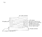
- Fig. 1 is a schematic diagram exemplifying the structure of an organic EL element used for an organic EL lighting device.
- the organic EL element shown in Fig. 1 is composed of glass substrate 100; transparent electrode (ITO) 101 that is made of a transparent member and that becomes an anode; hole injection layer 102; hole transporting layer 103; cathode 107; light emission layer 104 that emits light upon application of a predetermined voltage between transparent electrode 101 and cathode 107; electron transporting layer 105; electron injection layer 106; sealing agent 108; and sealing substrate 109.
- ITO transparent electrode
- Organic EL lighting devices are generally provided with a plurality of organic EL elements arranged as shown in Fig. 1 .
- the present invention is a manufacturing method for an organic EL lighting device that allows portions prone to shortcircuits to be automatically repaired while they are being aged in order to prevent the occurrence of the foregoing shortcircuits.
- anodes of a plurality of organic EL elements are electrically connected together.
- Fig. 2 is a schematic diagram that exemplifies the structure in which anodes of a plurality of organic EL elements are connected together.
- organic EL elements 200 each have an anode and a cathode.
- the anodes of organic EL elements 200 are connected together.
- the anodes may lie in a float state or have a predetermined reference potential (for example, they may be grounded or a predetermined voltage may be applied thereto).
- a forward bias voltage relative to the potential of the anodes and a reverse bias voltage thereof are alternately applied to the cathodes of organic EL elements 200 at a predetermined period.
- the reverse bias voltage be equal to or lower than the breakdown voltage.
- the forward bias voltage be neatly equal to a voltage in the range from a voltage immediately before and after an element emits light to a voltage at which the polarity of the reverse bias voltage is inverted.
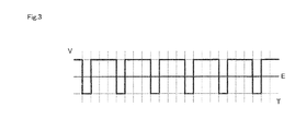
- Fig. 3 is a schematic diagram showing an example that represents a waveform of a voltage applied to the cathodes of the organic EL elements.
- voltage V forward bias voltage and reverse bias voltage
- voltage V reverse bias voltage and reverse bias voltage
- the ratio of the time for which the forward bias voltage is applied and the time for which the reverse bias voltage is applied is 3 : 1.
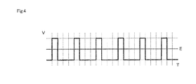
- Fig. 4 is a schematic diagram further exemplifying a waveform of a voltage applied to the cathodes of the organic EL elements.
- voltage V forward bias voltage and reverse bias voltage
- voltage V reverse bias voltage and reverse bias voltage
- the ratio of the time for which the forward bias voltage is applied and the time for which the reverse bias voltage is applied is 1 : 3.
- the ratio of the time for which the reverse bias voltage is applied to the cathodes to the time for which the forward bias voltage is applied to the cathodes with respect to the voltage having the waveform shown in Fig. 4 is greater than that with respect to the voltage having the waveform shown in Fig. 3 .
- the time for which the reverse bias voltage is applied to the cathodes with respect to the voltage having the waveform shown in Fig. 4 is greater than that with respect to the voltage having the waveform shown in Fig. 3 .
- the ratio of the time for which the reverse bias voltage is applied and the time for which the forward bias voltage is applied is increased so as to prevent elements, to which such repairing voltages have been applied, do not themselves break down.
- the ratio of the time for which the reverse bias voltage is applied and the time for which the forward bias voltage is applied may be increased successively or stepwise.
- An organic EL element can be represented by an equivalent circuit in which a diode and a capacitor are connected in parallel.
- an organic EL element has the structure of a capacitor in which an organic thin film is sandwiched between an anode thin film and a cathode thin film, it is difficult to form thin films having equal thicknesses in the order of nm. The thicknesses of each film is uneven. The lower the film thickness, the lower is the withstand voltage. The film thicknesses vary, and so do the withstand voltages.
- Fig. 5 is a schematic diagram further exemplifying a waveform of a voltage applied to the cathodes of the organic EL elements.
- voltage V forward bias voltage and reverse bias voltage
- voltage V that has a triangular wave with a predetermined period relative to potential E of the anodes may be applied to the cathodes.
- Fig. 6 is a schematic diagram further exemplifying a waveform of a voltage applied to the cathodes of the organic EL elements.
- voltage V that has a step-shaped waveform may be applied to the cathodes.
- Fig. 7 is a schematic diagram further exemplifying a waveform of a voltage applied to the cathodes of the organic EL elements.
- voltage V that has a pulse wave with a predetermined time width may be applied to the cathodes.
- a forward bias voltage may be applied to cathodes of half of a plurality of organic EL elements and a reverse bias voltage may be applied to cathodes of the other half of the organic EL elements.
- Fig. 8 is a schematic diagram exemplifying connections that cause a forward bias voltage to be applied to cathodes of half of a plurality of organic EL elements and a reverse bias voltage to be applied to cathodes of the other half of the organic EL elements.
- Fig. 8 symbolizes diodes of eight organic EL elements.
- Anodes of the organic EL elements are connected together to a common wire (Column).
- Cathodes of half (four organic EL elements) of the eight organic EL elements are connected to Row 1
- cathodes of the other half (four organic EL elements) of the eight organic EL elements are connected to Row 2.
- a voltage having a High level relative to the potential of Column is applied to Row 1
- a voltage having a Low level relative to the potential of Column is applied to Row 2.
- a forward bias voltage is applied to the organic EL elements connected to Row 2 and thereby a current flows in the arrow direction shown in Fig. 8 .
- the reverse bias voltage can be adjusted by increasing the ratio of the time for which the reverse bias voltage is applied and the time for which the forward bias voltage is applied so as to improve the likelihood of repairing the elements.
- cathodes on each row (column) of a plurality of organic EL elements arranged in a matrix shape may be connected together and a forward bias voltage and a reverse bias voltage may be alternately applied to the adjacent rows (columns).
- cathodes on each row of a plurality of organic EL elements arranged in a matrix shape may be connected together and a forward bias voltage and a reverse bias voltage may be alternately applied to the electrodes on the adjacent rows.
- Fig. 9 is a schematic diagram viewed from the cathode side of the structure of an organic EL lighting device in which cathodes on each row of a plurality of organic EL element arranged in a matrix shape are connected together and anodes of the organic EL elements are connected together.
- Fig. 10 is a schematic diagram viewed from the anode side of the structure of an organic EL lighting device in which cathodes on each row of a plurality of organic EL element arranged in a matrix shape are connected together and anodes of the organic EL elements are connected together.
- cathodes on each row of organic EL elements 200 arranged in a matrix shape are connected together to corresponding cathode connection line 202.
- anodes of organic EL elements 200 arranged in the matrix shape are connected together to anode connection line 201.
- Fig. 11 is a schematic diagram showing that a forward bias voltage and a reverse bias voltage are applied to the cathodes of the organic EL elements connected as shown in Fig. 9 .
- a forward bias voltage having a High level relative to the potential of the anodes is applied to the cathodes on rows 1, 3, and 5 that are odd number rows of the matrix.
- a reverse bias voltage having a Low level is applied to the cathodes on rows 2, 4, and 6 that are even number rows of the matrix.
- anode connection line 201 is grounded or placed in a float state.
- a voltage having a High level and a voltage having a Low level are alternately applied to the cathodes.
- Fig. 12 is a schematic diagram exemplifying a waveform of a voltage applied to each row (cathode) of the structure shown in Fig. 11 .
- waveforms of voltages applied to rows 5 and 6 shown in Fig. 11 are omitted.
- the waveform of the voltage applied to each row (cathode) of the structure shown in Fig. 11 is a square wave of which a voltage having a High level and a voltage having a Low level are alternately and periodically applied.
- the waveform of the voltage applied to row 1 is the same as that applied to row 3, whereas the waveform of the voltage applied to row 2 is the same as that applied to row 4.
- voltages (a voltage having a High level and a voltage having a Low level) are alternatively and periodically applied.
- a forward bias voltage is applied to an organic EL element to which a voltage having a Low voltage is applied
- a reverse bias voltage is applied to an organic EL element to which a voltage having a High level is applied.
- a current intensively flows reversely from portions prone to leakage or shortcircuits and thus the portions are repaired.
- voltages whose Low level and High level have been inverted are applied such that the portions that have not been repaired are repaired.
- the reverse bias voltage can be adjusted by increasing the ratio of the time for which the reverse bias voltage is applied and the time for which the forward bias voltage is applied so as to improve the likelihood of repairing the elements.
- Fig. 13 is a schematic diagram further exemplifying a waveform of a voltage applied to each row (cathode) of the structure shown in Fig. 11 .
- waveforms of voltages applied to rows 5 and 6 shown in Fig. 11 are omitted.
- the waveform of the voltage applied to each row (cathode) of the structure shown in Fig. 11 is a square wave in which a voltage having a High level and a voltage having a Low level are alternately and periodically applied. However, the timing at which the voltage applied to each row is shifted by a predetermined period.
- the cathode of an organic EL element is generally made of a metal foil of Al or the like. Since the specific resistance of a metal foil is lower than that of the anode side, a current tends to easily flow in the cathode relative to the anode. In addition, since heat can cause a metal foil to evaporate, the melting point of the material is low, localized electric field and concentrated current cause migration and thereby the element can be securely repaired. When connected cathodes are scanned, currents of all anode lines are extracted through one wire. Thus, since a current having a high density instantaneously flows, the likelihood repairing the elements improves.
- organic EL elements are being aged, they can be self-repaired unlike the structure of the related art in which they are repaired using laser light after shortcircuits occur therein. In addition, since many organic EL elements can be simultaneously repaired, the manufacturing takt time can be shortened.
- a surface lighting device according to the present invention can be applied to an organic EL lighting device, a backlight for a liquid display, and so forth.
Landscapes
- Engineering & Computer Science (AREA)
- Physics & Mathematics (AREA)
- Computer Hardware Design (AREA)
- General Physics & Mathematics (AREA)
- Theoretical Computer Science (AREA)
- Manufacturing & Machinery (AREA)
- Electroluminescent Light Sources (AREA)
Applications Claiming Priority (2)
| Application Number | Priority Date | Filing Date | Title |
|---|---|---|---|
| JP2010126735 | 2010-06-02 | ||
| PCT/JP2011/060204 WO2011152162A1 (ja) | 2010-06-02 | 2011-04-27 | 有機el照明装置の製造方法 |
Publications (3)
| Publication Number | Publication Date |
|---|---|
| EP2579685A1 true EP2579685A1 (de) | 2013-04-10 |
| EP2579685A4 EP2579685A4 (de) | 2018-01-17 |
| EP2579685B1 EP2579685B1 (de) | 2018-10-24 |
Family
ID=45066545
Family Applications (1)
| Application Number | Title | Priority Date | Filing Date |
|---|---|---|---|
| EP11789571.4A Not-in-force EP2579685B1 (de) | 2010-06-02 | 2011-04-27 | Verfahren zur herstellung einer organischen el-beleuchtungsvorrichtung |
Country Status (4)
| Country | Link |
|---|---|
| US (2) | US8845379B2 (de) |
| EP (1) | EP2579685B1 (de) |
| JP (1) | JP5911105B2 (de) |
| WO (1) | WO2011152162A1 (de) |
Families Citing this family (3)
| Publication number | Priority date | Publication date | Assignee | Title |
|---|---|---|---|---|
| JP6366088B2 (ja) * | 2014-03-28 | 2018-08-01 | Necライティング株式会社 | 有機el素子のリペア方法、有機elパネルの製造方法、及び発光装置 |
| US10036867B2 (en) | 2016-08-31 | 2018-07-31 | International Business Machines Corporation | Illuminating cable for enhanced traceability |
| JP7048246B2 (ja) * | 2017-10-05 | 2022-04-05 | メルク パテント ゲゼルシャフト ミット ベシュレンクテル ハフツング | 発光システム |
Family Cites Families (16)
| Publication number | Priority date | Publication date | Assignee | Title |
|---|---|---|---|---|
| JPS58113094U (ja) | 1982-01-23 | 1983-08-02 | ヤマハ株式会社 | 楽器ケ−ス |
| JPH0451490Y2 (de) | 1986-01-31 | 1992-12-03 | ||
| JP2818255B2 (ja) * | 1990-05-08 | 1998-10-30 | 出光興産株式会社 | 有機エレクトロルミネッセンス素子の製造方法 |
| JPH0451490A (ja) | 1990-06-19 | 1992-02-19 | Ricoh Co Ltd | 有機薄膜型電界発光素子の駆動方法 |
| JPH051490A (ja) | 1991-06-25 | 1993-01-08 | Sekisui Chem Co Ltd | 出窓の取付方法 |
| JPH11162637A (ja) * | 1997-11-25 | 1999-06-18 | Matsushita Electron Corp | 有機発光ダイオードの修復方法 |
| TW530427B (en) * | 2000-10-10 | 2003-05-01 | Semiconductor Energy Lab | Method of fabricating and/or repairing a light emitting device |
| JP4152165B2 (ja) | 2002-10-24 | 2008-09-17 | オプトレックス株式会社 | 有機el表示装置の製造方法 |
| JP4154215B2 (ja) | 2002-11-12 | 2008-09-24 | オプトレックス株式会社 | 有機エレクトロルミネッセンス表示素子の製造方法 |
| JP2004247088A (ja) | 2003-02-12 | 2004-09-02 | Denso Corp | 有機elパネルの製造方法 |
| JP4545535B2 (ja) | 2003-09-19 | 2010-09-15 | 株式会社半導体エネルギー研究所 | 製造装置 |
| JP4666247B2 (ja) | 2004-03-31 | 2011-04-06 | 日本精機株式会社 | 有機elパネルの製造方法 |
| JP4569194B2 (ja) | 2004-04-28 | 2010-10-27 | ソニー株式会社 | 発光装置の修復方法及び製造方法、発光装置の修復装置及び製造装置 |
| JP2007141536A (ja) | 2005-11-16 | 2007-06-07 | Nippon Seiki Co Ltd | 有機elパネルの製造方法 |
| JP2007207703A (ja) * | 2006-02-06 | 2007-08-16 | Sharp Corp | 有機エレクトロルミネッセンス装置の修復方法 |
| JP2010126735A (ja) | 2008-11-25 | 2010-06-10 | Fukuoka Prefecture | ナノ粒子薄膜の製造方法、ナノ粒子薄膜及びそれを用いた電子デバイス |
-
2011
- 2011-04-27 EP EP11789571.4A patent/EP2579685B1/de not_active Not-in-force
- 2011-04-27 WO PCT/JP2011/060204 patent/WO2011152162A1/ja not_active Ceased
- 2011-04-27 JP JP2012518298A patent/JP5911105B2/ja active Active
- 2011-04-27 US US13/700,635 patent/US8845379B2/en active Active
-
2014
- 2014-09-04 US US14/477,278 patent/US9196875B2/en active Active
Non-Patent Citations (1)
| Title |
|---|
| See references of WO2011152162A1 * |
Also Published As
| Publication number | Publication date |
|---|---|
| WO2011152162A1 (ja) | 2011-12-08 |
| EP2579685B1 (de) | 2018-10-24 |
| JP5911105B2 (ja) | 2016-04-27 |
| EP2579685A4 (de) | 2018-01-17 |
| JPWO2011152162A1 (ja) | 2013-07-25 |
| US20130072078A1 (en) | 2013-03-21 |
| US9196875B2 (en) | 2015-11-24 |
| US8845379B2 (en) | 2014-09-30 |
| US20140370622A1 (en) | 2014-12-18 |
Similar Documents
| Publication | Publication Date | Title |
|---|---|---|
| CN104112426A (zh) | Oled像素驱动电路、静电释放保护电路及检测方法 | |
| CN101982013A (zh) | 发光装置 | |
| US9196875B2 (en) | Manufacturing method for organic EL lighting device | |
| JP2005173299A (ja) | 有機el表示装置および有機el表示装置の基板 | |
| JP3606309B2 (ja) | 有機薄膜発光ディスプレイ | |
| JP4455165B2 (ja) | 有機el表示装置用基板および有機el表示装置 | |
| JP2001196191A (ja) | 有機薄膜発光ディスプレイおよびその製造方法 | |
| CN108054187B (zh) | 显示面板及其坏点处理方法、显示装置 | |
| CN111149210B (zh) | 制造oled器件的方法 | |
| JP2006222015A (ja) | 発光表示パネル、及び発光表示パネルの検査方法 | |
| JP3633841B2 (ja) | 有機薄膜発光ディスプレイの修復方法 | |
| JP5024529B2 (ja) | 表示装置の製造方法およびtftアレイ基板の製造方法 | |
| JP2011164231A (ja) | 表示パネル用マトリクス回路基板、表示パネル及びそれらの製造方法 | |
| US20110163337A1 (en) | Architecture for organic electronic devices | |
| JP4560306B2 (ja) | 有機el表示素子用基板及び有機el表示素子の製造方法 | |
| CN101866917B (zh) | 主动元件阵列基板及其修补方法 | |
| JP4499490B2 (ja) | 有機el表示装置用基板および有機el表示装置 | |
| US9741933B2 (en) | Method for repairing organic EL element, method for manufacturing organic EL panel, and light-emitting device | |
| JP2005310659A (ja) | 有機elパネルの製造方法 | |
| JP4486833B2 (ja) | 有機el表示素子用基板及び有機el表示素子の製造方法 | |
| JP4826079B2 (ja) | 有機el素子の製造方法 | |
| JP2004247088A (ja) | 有機elパネルの製造方法 | |
| JP4742505B2 (ja) | 単純マトリクス型表示パネルの駆動装置及び駆動方法 | |
| KR102126551B1 (ko) | 박막 트랜지스터의 리페어 방법 | |
| JP4410186B2 (ja) | 発光ディスプレイの駆動方法 |
Legal Events
| Date | Code | Title | Description |
|---|---|---|---|
| PUAI | Public reference made under article 153(3) epc to a published international application that has entered the european phase |
Free format text: ORIGINAL CODE: 0009012 |
|
| 17P | Request for examination filed |
Effective date: 20121126 |
|
| AK | Designated contracting states |
Kind code of ref document: A1 Designated state(s): AL AT BE BG CH CY CZ DE DK EE ES FI FR GB GR HR HU IE IS IT LI LT LU LV MC MK MT NL NO PL PT RO RS SE SI SK SM TR |
|
| DAX | Request for extension of the european patent (deleted) | ||
| RA4 | Supplementary search report drawn up and despatched (corrected) |
Effective date: 20171220 |
|
| RIC1 | Information provided on ipc code assigned before grant |
Ipc: H01L 51/56 20060101AFI20171214BHEP Ipc: H05B 33/10 20060101ALI20171214BHEP Ipc: F21Y 105/00 20160101ALI20171214BHEP |
|
| REG | Reference to a national code |
Ref country code: DE Ref legal event code: R079 Ref document number: 602011053246 Country of ref document: DE Free format text: PREVIOUS MAIN CLASS: H05B0033100000 Ipc: H01L0051560000 |
|
| GRAP | Despatch of communication of intention to grant a patent |
Free format text: ORIGINAL CODE: EPIDOSNIGR1 |
|
| STAA | Information on the status of an ep patent application or granted ep patent |
Free format text: STATUS: GRANT OF PATENT IS INTENDED |
|
| RIC1 | Information provided on ipc code assigned before grant |
Ipc: F21Y 105/00 20060101ALI20180531BHEP Ipc: G09G 3/00 20060101ALI20180531BHEP Ipc: H01L 51/56 20060101AFI20180531BHEP Ipc: H05B 33/10 20060101ALI20180531BHEP |
|
| INTG | Intention to grant announced |
Effective date: 20180625 |
|
| GRAS | Grant fee paid |
Free format text: ORIGINAL CODE: EPIDOSNIGR3 |
|
| GRAA | (expected) grant |
Free format text: ORIGINAL CODE: 0009210 |
|
| STAA | Information on the status of an ep patent application or granted ep patent |
Free format text: STATUS: THE PATENT HAS BEEN GRANTED |
|
| AK | Designated contracting states |
Kind code of ref document: B1 Designated state(s): AL AT BE BG CH CY CZ DE DK EE ES FI FR GB GR HR HU IE IS IT LI LT LU LV MC MK MT NL NO PL PT RO RS SE SI SK SM TR |
|
| REG | Reference to a national code |
Ref country code: GB Ref legal event code: FG4D |
|
| REG | Reference to a national code |
Ref country code: CH Ref legal event code: EP |
|
| REG | Reference to a national code |
Ref country code: IE Ref legal event code: FG4D |
|
| REG | Reference to a national code |
Ref country code: AT Ref legal event code: REF Ref document number: 1057736 Country of ref document: AT Kind code of ref document: T Effective date: 20181115 |
|
| REG | Reference to a national code |
Ref country code: DE Ref legal event code: R096 Ref document number: 602011053246 Country of ref document: DE |
|
| REG | Reference to a national code |
Ref country code: NL Ref legal event code: MP Effective date: 20181024 |
|
| REG | Reference to a national code |
Ref country code: LT Ref legal event code: MG4D |
|
| REG | Reference to a national code |
Ref country code: AT Ref legal event code: MK05 Ref document number: 1057736 Country of ref document: AT Kind code of ref document: T Effective date: 20181024 |
|
| PG25 | Lapsed in a contracting state [announced via postgrant information from national office to epo] |
Ref country code: NL Free format text: LAPSE BECAUSE OF FAILURE TO SUBMIT A TRANSLATION OF THE DESCRIPTION OR TO PAY THE FEE WITHIN THE PRESCRIBED TIME-LIMIT Effective date: 20181024 |
|
| PG25 | Lapsed in a contracting state [announced via postgrant information from national office to epo] |
Ref country code: ES Free format text: LAPSE BECAUSE OF FAILURE TO SUBMIT A TRANSLATION OF THE DESCRIPTION OR TO PAY THE FEE WITHIN THE PRESCRIBED TIME-LIMIT Effective date: 20181024 Ref country code: LV Free format text: LAPSE BECAUSE OF FAILURE TO SUBMIT A TRANSLATION OF THE DESCRIPTION OR TO PAY THE FEE WITHIN THE PRESCRIBED TIME-LIMIT Effective date: 20181024 Ref country code: FI Free format text: LAPSE BECAUSE OF FAILURE TO SUBMIT A TRANSLATION OF THE DESCRIPTION OR TO PAY THE FEE WITHIN THE PRESCRIBED TIME-LIMIT Effective date: 20181024 Ref country code: LT Free format text: LAPSE BECAUSE OF FAILURE TO SUBMIT A TRANSLATION OF THE DESCRIPTION OR TO PAY THE FEE WITHIN THE PRESCRIBED TIME-LIMIT Effective date: 20181024 Ref country code: HR Free format text: LAPSE BECAUSE OF FAILURE TO SUBMIT A TRANSLATION OF THE DESCRIPTION OR TO PAY THE FEE WITHIN THE PRESCRIBED TIME-LIMIT Effective date: 20181024 Ref country code: PL Free format text: LAPSE BECAUSE OF FAILURE TO SUBMIT A TRANSLATION OF THE DESCRIPTION OR TO PAY THE FEE WITHIN THE PRESCRIBED TIME-LIMIT Effective date: 20181024 Ref country code: BG Free format text: LAPSE BECAUSE OF FAILURE TO SUBMIT A TRANSLATION OF THE DESCRIPTION OR TO PAY THE FEE WITHIN THE PRESCRIBED TIME-LIMIT Effective date: 20190124 Ref country code: AT Free format text: LAPSE BECAUSE OF FAILURE TO SUBMIT A TRANSLATION OF THE DESCRIPTION OR TO PAY THE FEE WITHIN THE PRESCRIBED TIME-LIMIT Effective date: 20181024 Ref country code: IS Free format text: LAPSE BECAUSE OF FAILURE TO SUBMIT A TRANSLATION OF THE DESCRIPTION OR TO PAY THE FEE WITHIN THE PRESCRIBED TIME-LIMIT Effective date: 20190224 Ref country code: NO Free format text: LAPSE BECAUSE OF FAILURE TO SUBMIT A TRANSLATION OF THE DESCRIPTION OR TO PAY THE FEE WITHIN THE PRESCRIBED TIME-LIMIT Effective date: 20190124 |
|
| PG25 | Lapsed in a contracting state [announced via postgrant information from national office to epo] |
Ref country code: RS Free format text: LAPSE BECAUSE OF FAILURE TO SUBMIT A TRANSLATION OF THE DESCRIPTION OR TO PAY THE FEE WITHIN THE PRESCRIBED TIME-LIMIT Effective date: 20181024 Ref country code: PT Free format text: LAPSE BECAUSE OF FAILURE TO SUBMIT A TRANSLATION OF THE DESCRIPTION OR TO PAY THE FEE WITHIN THE PRESCRIBED TIME-LIMIT Effective date: 20190224 Ref country code: GR Free format text: LAPSE BECAUSE OF FAILURE TO SUBMIT A TRANSLATION OF THE DESCRIPTION OR TO PAY THE FEE WITHIN THE PRESCRIBED TIME-LIMIT Effective date: 20190125 Ref country code: AL Free format text: LAPSE BECAUSE OF FAILURE TO SUBMIT A TRANSLATION OF THE DESCRIPTION OR TO PAY THE FEE WITHIN THE PRESCRIBED TIME-LIMIT Effective date: 20181024 Ref country code: SE Free format text: LAPSE BECAUSE OF FAILURE TO SUBMIT A TRANSLATION OF THE DESCRIPTION OR TO PAY THE FEE WITHIN THE PRESCRIBED TIME-LIMIT Effective date: 20181024 |
|
| REG | Reference to a national code |
Ref country code: DE Ref legal event code: R097 Ref document number: 602011053246 Country of ref document: DE |
|
| PG25 | Lapsed in a contracting state [announced via postgrant information from national office to epo] |
Ref country code: IT Free format text: LAPSE BECAUSE OF FAILURE TO SUBMIT A TRANSLATION OF THE DESCRIPTION OR TO PAY THE FEE WITHIN THE PRESCRIBED TIME-LIMIT Effective date: 20181024 Ref country code: CZ Free format text: LAPSE BECAUSE OF FAILURE TO SUBMIT A TRANSLATION OF THE DESCRIPTION OR TO PAY THE FEE WITHIN THE PRESCRIBED TIME-LIMIT Effective date: 20181024 Ref country code: DK Free format text: LAPSE BECAUSE OF FAILURE TO SUBMIT A TRANSLATION OF THE DESCRIPTION OR TO PAY THE FEE WITHIN THE PRESCRIBED TIME-LIMIT Effective date: 20181024 |
|
| PG25 | Lapsed in a contracting state [announced via postgrant information from national office to epo] |
Ref country code: EE Free format text: LAPSE BECAUSE OF FAILURE TO SUBMIT A TRANSLATION OF THE DESCRIPTION OR TO PAY THE FEE WITHIN THE PRESCRIBED TIME-LIMIT Effective date: 20181024 Ref country code: SM Free format text: LAPSE BECAUSE OF FAILURE TO SUBMIT A TRANSLATION OF THE DESCRIPTION OR TO PAY THE FEE WITHIN THE PRESCRIBED TIME-LIMIT Effective date: 20181024 Ref country code: SK Free format text: LAPSE BECAUSE OF FAILURE TO SUBMIT A TRANSLATION OF THE DESCRIPTION OR TO PAY THE FEE WITHIN THE PRESCRIBED TIME-LIMIT Effective date: 20181024 Ref country code: RO Free format text: LAPSE BECAUSE OF FAILURE TO SUBMIT A TRANSLATION OF THE DESCRIPTION OR TO PAY THE FEE WITHIN THE PRESCRIBED TIME-LIMIT Effective date: 20181024 |
|
| PLBE | No opposition filed within time limit |
Free format text: ORIGINAL CODE: 0009261 |
|
| STAA | Information on the status of an ep patent application or granted ep patent |
Free format text: STATUS: NO OPPOSITION FILED WITHIN TIME LIMIT |
|
| 26N | No opposition filed |
Effective date: 20190725 |
|
| PG25 | Lapsed in a contracting state [announced via postgrant information from national office to epo] |
Ref country code: SI Free format text: LAPSE BECAUSE OF FAILURE TO SUBMIT A TRANSLATION OF THE DESCRIPTION OR TO PAY THE FEE WITHIN THE PRESCRIBED TIME-LIMIT Effective date: 20181024 |
|
| REG | Reference to a national code |
Ref country code: CH Ref legal event code: PL |
|
| REG | Reference to a national code |
Ref country code: BE Ref legal event code: MM Effective date: 20190430 |
|
| GBPC | Gb: european patent ceased through non-payment of renewal fee |
Effective date: 20190427 |
|
| PG25 | Lapsed in a contracting state [announced via postgrant information from national office to epo] |
Ref country code: LU Free format text: LAPSE BECAUSE OF NON-PAYMENT OF DUE FEES Effective date: 20190427 Ref country code: MC Free format text: LAPSE BECAUSE OF FAILURE TO SUBMIT A TRANSLATION OF THE DESCRIPTION OR TO PAY THE FEE WITHIN THE PRESCRIBED TIME-LIMIT Effective date: 20181024 |
|
| PG25 | Lapsed in a contracting state [announced via postgrant information from national office to epo] |
Ref country code: CH Free format text: LAPSE BECAUSE OF NON-PAYMENT OF DUE FEES Effective date: 20190430 Ref country code: GB Free format text: LAPSE BECAUSE OF NON-PAYMENT OF DUE FEES Effective date: 20190427 Ref country code: LI Free format text: LAPSE BECAUSE OF NON-PAYMENT OF DUE FEES Effective date: 20190430 |
|
| REG | Reference to a national code |
Ref country code: DE Ref legal event code: R082 Ref document number: 602011053246 Country of ref document: DE Representative=s name: VOSSIUS & PARTNER PATENTANWAELTE RECHTSANWAELT, DE Ref country code: DE Ref legal event code: R081 Ref document number: 602011053246 Country of ref document: DE Owner name: HOTALUX, LTD., JP Free format text: FORMER OWNER: NEC LIGHTING, LTD., TOKYO, JP |
|
| PG25 | Lapsed in a contracting state [announced via postgrant information from national office to epo] |
Ref country code: BE Free format text: LAPSE BECAUSE OF NON-PAYMENT OF DUE FEES Effective date: 20190430 |
|
| PG25 | Lapsed in a contracting state [announced via postgrant information from national office to epo] |
Ref country code: TR Free format text: LAPSE BECAUSE OF FAILURE TO SUBMIT A TRANSLATION OF THE DESCRIPTION OR TO PAY THE FEE WITHIN THE PRESCRIBED TIME-LIMIT Effective date: 20181024 |
|
| PG25 | Lapsed in a contracting state [announced via postgrant information from national office to epo] |
Ref country code: IE Free format text: LAPSE BECAUSE OF NON-PAYMENT OF DUE FEES Effective date: 20190427 |
|
| PG25 | Lapsed in a contracting state [announced via postgrant information from national office to epo] |
Ref country code: FR Free format text: LAPSE BECAUSE OF NON-PAYMENT OF DUE FEES Effective date: 20190430 |
|
| PG25 | Lapsed in a contracting state [announced via postgrant information from national office to epo] |
Ref country code: CY Free format text: LAPSE BECAUSE OF FAILURE TO SUBMIT A TRANSLATION OF THE DESCRIPTION OR TO PAY THE FEE WITHIN THE PRESCRIBED TIME-LIMIT Effective date: 20181024 |
|
| PG25 | Lapsed in a contracting state [announced via postgrant information from national office to epo] |
Ref country code: MT Free format text: LAPSE BECAUSE OF FAILURE TO SUBMIT A TRANSLATION OF THE DESCRIPTION OR TO PAY THE FEE WITHIN THE PRESCRIBED TIME-LIMIT Effective date: 20181024 Ref country code: HU Free format text: LAPSE BECAUSE OF FAILURE TO SUBMIT A TRANSLATION OF THE DESCRIPTION OR TO PAY THE FEE WITHIN THE PRESCRIBED TIME-LIMIT; INVALID AB INITIO Effective date: 20110427 |
|
| PG25 | Lapsed in a contracting state [announced via postgrant information from national office to epo] |
Ref country code: MK Free format text: LAPSE BECAUSE OF FAILURE TO SUBMIT A TRANSLATION OF THE DESCRIPTION OR TO PAY THE FEE WITHIN THE PRESCRIBED TIME-LIMIT Effective date: 20181024 |
|
| REG | Reference to a national code |
Ref country code: DE Ref legal event code: R079 Ref document number: 602011053246 Country of ref document: DE Free format text: PREVIOUS MAIN CLASS: H01L0051560000 Ipc: H10K0050000000 |
|
| PGFP | Annual fee paid to national office [announced via postgrant information from national office to epo] |
Ref country code: DE Payment date: 20240306 Year of fee payment: 14 |
|
| REG | Reference to a national code |
Ref country code: DE Ref legal event code: R119 Ref document number: 602011053246 Country of ref document: DE |
|
| PG25 | Lapsed in a contracting state [announced via postgrant information from national office to epo] |
Ref country code: DE Free format text: LAPSE BECAUSE OF NON-PAYMENT OF DUE FEES Effective date: 20251104 |