EP2579308A2 - Halbleiterbauelementen-Stapel - Google Patents
Halbleiterbauelementen-Stapel Download PDFInfo
- Publication number
- EP2579308A2 EP2579308A2 EP12186166.0A EP12186166A EP2579308A2 EP 2579308 A2 EP2579308 A2 EP 2579308A2 EP 12186166 A EP12186166 A EP 12186166A EP 2579308 A2 EP2579308 A2 EP 2579308A2
- Authority
- EP
- European Patent Office
- Prior art keywords
- semiconductor device
- major surface
- probe pad
- stacked
- edge
- Prior art date
- Legal status (The legal status is an assumption and is not a legal conclusion. Google has not performed a legal analysis and makes no representation as to the accuracy of the status listed.)
- Withdrawn
Links
Images



Classifications
-
- H—ELECTRICITY
- H10—SEMICONDUCTOR DEVICES; ELECTRIC SOLID-STATE DEVICES NOT OTHERWISE PROVIDED FOR
- H10W—GENERIC PACKAGES, INTERCONNECTIONS, CONNECTORS OR OTHER CONSTRUCTIONAL DETAILS OF DEVICES COVERED BY CLASS H10
- H10W90/00—Package configurations
-
- H—ELECTRICITY
- H10—SEMICONDUCTOR DEVICES; ELECTRIC SOLID-STATE DEVICES NOT OTHERWISE PROVIDED FOR
- H10P—GENERIC PROCESSES OR APPARATUS FOR THE MANUFACTURE OR TREATMENT OF DEVICES COVERED BY CLASS H10
- H10P74/00—Testing or measuring during manufacture or treatment of wafers, substrates or devices
- H10P74/27—Structural arrangements therefor
- H10P74/273—Interconnections for measuring or testing, e.g. probe pads
-
- H—ELECTRICITY
- H10—SEMICONDUCTOR DEVICES; ELECTRIC SOLID-STATE DEVICES NOT OTHERWISE PROVIDED FOR
- H10W—GENERIC PACKAGES, INTERCONNECTIONS, CONNECTORS OR OTHER CONSTRUCTIONAL DETAILS OF DEVICES COVERED BY CLASS H10
- H10W20/00—Interconnections in chips, wafers or substrates
- H10W20/01—Manufacture or treatment
- H10W20/021—Manufacture or treatment of interconnections within wafers or substrates
- H10W20/023—Manufacture or treatment of interconnections within wafers or substrates the interconnections being through-semiconductor vias
-
- H—ELECTRICITY
- H10—SEMICONDUCTOR DEVICES; ELECTRIC SOLID-STATE DEVICES NOT OTHERWISE PROVIDED FOR
- H10W—GENERIC PACKAGES, INTERCONNECTIONS, CONNECTORS OR OTHER CONSTRUCTIONAL DETAILS OF DEVICES COVERED BY CLASS H10
- H10W20/00—Interconnections in chips, wafers or substrates
- H10W20/01—Manufacture or treatment
- H10W20/021—Manufacture or treatment of interconnections within wafers or substrates
- H10W20/023—Manufacture or treatment of interconnections within wafers or substrates the interconnections being through-semiconductor vias
- H10W20/0238—Manufacture or treatment of interconnections within wafers or substrates the interconnections being through-semiconductor vias comprising etching via holes through pads or through electrodes
-
- H—ELECTRICITY
- H10—SEMICONDUCTOR DEVICES; ELECTRIC SOLID-STATE DEVICES NOT OTHERWISE PROVIDED FOR
- H10W—GENERIC PACKAGES, INTERCONNECTIONS, CONNECTORS OR OTHER CONSTRUCTIONAL DETAILS OF DEVICES COVERED BY CLASS H10
- H10W90/00—Package configurations
- H10W90/20—Configurations of stacked chips
-
- H—ELECTRICITY
- H10—SEMICONDUCTOR DEVICES; ELECTRIC SOLID-STATE DEVICES NOT OTHERWISE PROVIDED FOR
- H10W—GENERIC PACKAGES, INTERCONNECTIONS, CONNECTORS OR OTHER CONSTRUCTIONAL DETAILS OF DEVICES COVERED BY CLASS H10
- H10W90/00—Package configurations
- H10W90/20—Configurations of stacked chips
- H10W90/284—Configurations of stacked chips characterised by structural arrangements for measuring or testing
-
- H—ELECTRICITY
- H10—SEMICONDUCTOR DEVICES; ELECTRIC SOLID-STATE DEVICES NOT OTHERWISE PROVIDED FOR
- H10W—GENERIC PACKAGES, INTERCONNECTIONS, CONNECTORS OR OTHER CONSTRUCTIONAL DETAILS OF DEVICES COVERED BY CLASS H10
- H10W90/00—Package configurations
- H10W90/20—Configurations of stacked chips
- H10W90/288—Configurations of stacked chips characterised by arrangements for thermal management of the stacked chips
-
- H—ELECTRICITY
- H10—SEMICONDUCTOR DEVICES; ELECTRIC SOLID-STATE DEVICES NOT OTHERWISE PROVIDED FOR
- H10W—GENERIC PACKAGES, INTERCONNECTIONS, CONNECTORS OR OTHER CONSTRUCTIONAL DETAILS OF DEVICES COVERED BY CLASS H10
- H10W90/00—Package configurations
- H10W90/20—Configurations of stacked chips
- H10W90/297—Configurations of stacked chips characterised by the through-semiconductor vias [TSVs] in the stacked chips
-
- H—ELECTRICITY
- H10—SEMICONDUCTOR DEVICES; ELECTRIC SOLID-STATE DEVICES NOT OTHERWISE PROVIDED FOR
- H10W—GENERIC PACKAGES, INTERCONNECTIONS, CONNECTORS OR OTHER CONSTRUCTIONAL DETAILS OF DEVICES COVERED BY CLASS H10
- H10W90/00—Package configurations
- H10W90/701—Package configurations characterised by the relative positions of pads or connectors relative to package parts
- H10W90/721—Package configurations characterised by the relative positions of pads or connectors relative to package parts of bump connectors
- H10W90/722—Package configurations characterised by the relative positions of pads or connectors relative to package parts of bump connectors between stacked chips
Definitions
- TSV through-silicon-via
- FIG. 1 is a partial side cross-sectional view of a semiconductor device after a phase of manufacture in accordance with an embodiment of the present invention.
- FIG. 2 is a partial side cross-sectional view of the semiconductor device of FIG. 1 after another phase of manufacture.
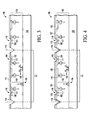
- FIG. 4 is a partial side cross-sectional view of the semiconductor device of FIG. 3 after another phase of manufacture.
- FIG. 7 is a partial side cross-sectional view of a group of stacked semiconductor device in accordance with an embodiment of the invention.
- Embodiments of a contiguous via plug through a die stack are disclosed that reduce the stack height and also improve high speed signaling performance. Thermal performance is improved by dissipating heat from conductive planes formed with beveled edges with a self-aligning heat sink. The beveled edges of the die also accommodate a self-aligning test probe that can be used to test functionality of the stacked semiconductor die.
- One or more layers of interconnects 106 can be formed to electrically couple active circuit components to other internal and/or external components. Electrical devices may also be formed in one or more dielectric layers. A dielectric or other insulating material can be formed in one or more layers as active surface and interconnect region 103 is formed to electrically isolate components from one another. A last layer of conductive interconnects including capture pads 108 is covered with passivation layer 110. Passivation layer 110 can be made of inorganic and/or organic layer of material such as silicon nitride, polyimide, or benzocyclobutene, to name a few.
- Substrate 102 may comprise, for example, bulk silicon, doped or undoped, or an active layer of a semiconductor-on-insulator (SOI) substrate.
- SOI substrate comprises a layer of a semiconductor material, such as silicon, formed on an insulator layer.
- the insulator layer may be, for example, a buried oxide (BOX) layer or a silicon oxide layer.
- BOX buried oxide
- the insulator layer is provided on a substrate, typically a silicon or glass substrate.
- Other substrates, such as a multi-layered or gradient substrate may also be used.
- a grid of die 111 may be formed on wafer 100, with die 111 separated from one another by scribe streets 112. Individual, independent semiconductor devices are formed by separating die 111 along scribe streets 112 once processing is completed.
- bevels 114 can be approximately 70 microns in length along a bevel 114 that is angled, for example at 45degrees, to the top surface of the semiconductor device.
- a probe pad (not shown) formed on the bevel 114 can be 45 microns in width and spaced at least 5 microns from the next closest probe pad on the bevel.
- Other suitable dimensions can be used for the probe contact tip and probe pads.
- FIG. 3 is a partial side cross-sectional view of the wafer 100 of FIG. 2 after another phase of manufacture in which openings 116 are formed around an opening 117 in capture pads 108. Openings 116 typically are larger than and extend beyond the opening 117 in capture pads 108. Openings 117 can be in the range of 2-20 microns in diameter and openings 116 can be in the range of 5-60 microns, or other suitable dimensions. Depending on the material used for passivation layer 110, openings 116 can be formed using a standard etch and/or photoimageable or patterning techniques.
- FIG. 5 is a partial side cross-sectional view A-A' of the wafer 100 of FIG. 6 after another phase of manufacture in which openings 116 are extended to create openings 502 for through substrate vias through active surface and interconnect region 103 and substrate 102.
- Openings 502 may be formed by etching or other suitable technique. It should be understood that the etch processes may be accomplished in single etch processes or multiple etch processes. It should also be understood that the openings 502 may be formed by other methods, such as milling, laser techniques, or the like.
- a layer of electrical isolation material such as an insulator layer 122 is formed on the sidewalls of openings 502.
- Insulator layer 122 may be formed using a CVD, spin-on coating or epitaxial process to form a dielectric layer that covers the sidewalls of the openings 116.
- the dielectric constant of the insulator layer 122 can be less than about 6 or other suitable value and may be formed, for example, of materials used to form interconnects, by any suitable method known in the art. Other suitable materials and application methods may be used for insulator layer 122.
- the insulator 122 also provides additional isolation between the conductive material and the substrate 102 thereby achieving a reduction in capacitance along the sidewall of the TSV.
- the relatively thin isolation structure of insulator 122 creates an increased effective area the conductive material of through silicon vias (TSV) 802 ( FIG. 8 ), thus increasing the effectiveness of the TSV 802.
- TSV through silicon vias
- FIG. 6 is a partial top view of single die 111 of FIG. 5 .
- Contact pads 118 are formed with a circular portion 602 having central opening 117, and a rectangular pad 604 extending from a subsection of the outer edge of circular portion 602 to bevels 114 ( FIG. 5 ).
- Other suitable shapes for contact pads 118 and openings 117 can be used.
- Gaps 121 between contact pads 118 and conductive plane 120 extend around the circular portion 602 of contact pads 118 to separate contact pads 118 from conductive plane 120.
- Conductive plane 120 typically covers inner sections of die 111 around contact pads 118, and in some sections, covers edge bevels 114. Die 111 will typically be independent of other circuitry/die on the wafer 100 after die 111 is singulated along scribe lines 112.
- FIG. 7 is a partial side cross-sectional view of a semiconductor device 700 that includes a group of stacked die 111 in wafers 100 in accordance with an embodiment of the invention in which openings 116, 502 ( FIG. 5 ) are aligned and coincident with one another to form a continuous opening through two or more die 111 in the stack.
- the top layer 126 of each wafer 100 faces the top layer 126 of an adjacent wafer 100.
- the bottoms of substrate102 of wafer 100 in the inner layers 706 face the bottoms of another wafer 100, while the bottom of the substrate 102 of wafer 100 at the top and bottom of semiconductor device 700 face outward and are thus exposed to the external environment.
- V-shaped openings 702 are formed by pairs of edge bevels 114 ( FIGS.
- Enlarged areas 704 are formed in the inner layers of semiconductor device 700 at the top of the openings 116 ( FIG. 5 ) surrounded by contact pads 118 aligned and pairs of edge bevels 114 facing one another to form V-shaped openings 702.
- the top layers 126 of wafers 100 may be joined using a suitable adhesive insulating material 710 such as glass, epoxy, polyimide, acrylic, silicone, or other suitable attachment, bonding or fastening technique.
- a suitable adhesive insulating material 710 such as glass, epoxy, polyimide, acrylic, silicone, or other suitable attachment, bonding or fastening technique.
- the bottom sides of wafers 100 may be joined to one another using a layer of adhesive 712 such as insulative materials like glass, epoxy, polyimide, acrylic, silicone, or conductive attachment material, such as solder or eutectic alloys, or other suitable attachment, bonding, mounting, or fastening techniques.
- FIG. 8 is a partial side cross-sectional view of semiconductor device 700 of FIG. 7 with openings 116, 502 ( FIG. 5 ) filled with conductive material after wafers 100 are stacked with openings 116, 502 aligned.
- Conductive material forms continuous through-silicon vias (TSVs) 802 through at least 2 of the stacked die 111 the semiconductor device 700.
- TSVs through-silicon vias
- any suitable material for conducting electrical and/or optical signals can be used to form TSVs 802 in openings 116, 117, 502, such as copper, copper alloys, aluminum, tungsten, silver, polysilicon, silicon, conductive polymers, doped carbon nanotubes, polyacrylates, polystyrenics, and combinations thereof.
- at least one via comprises an electrically conducting material and at least on other via comprises an optically conductive material such as silicon.
- One alternative is forming the conductive material in openings 116, 117, 502 by depositing a seed layer and then performing an electroplating process.
- TSVs 802 Other alternatives that can be used to form the conductive material in TSVs 802 include: fusible metal powder such as titanium or molybdenum powder; plastic balls coated with a conductive material, such as the Micropearl SOL product from Sekisui America Corporation in Mt. Laurel, New Jersey; reinforced solder columns, such as those available from Six Sigma Corporation in Milpitas, California; a core wire inserted through openings 116 as a seed layer combined with copper, conductive polymer, or other suitable electroplating process; and/or nickel nanotubes or nanotubes formed of carbon that can be doped with iodine or bromine to achieve the desired conductive properties
- a first die 111 When two die 111 are stacked face to face, a first die 111 is in a first orientation and a second die 111 is in a mirror image orientation relative to the first die.
- Die 111 can be configured so that the capture pads 108 for the first die 111 align to the mirror imaged capture pads 108 of the second die 111.
- capture pads 108 are aligned to the center spine of the die 111 so the capture pads 108 will align to corresponding inputs or outputs of the two die 111 after stacking.
- capture pads 108 functionally coupling address or data signals may be placed symmetrically away from the center spine of die 111 so that when active surfaces of first and second die 111 are stacked face to face, a first capture pad 108 coupling to first address input of said first die 111 will couple to a second address input of said second die 111 and second capture pads 108 of said first die 111 will couple to a first data input of said first die 111 and to a second data input of said second die 111.
- wafers 100 can be singulated, or separated into stacks of die 111 to allow individual stacks of die 111 to be tested.
- the term semiconductor device 700 as used herein can be considered a stack of die 111 or a stack of wafers 100. Additionally, some wafers 100 or die 111 in a stack may not include edge bevels 114, but may still be interspersed in a stack of wafers 100 and die 11 with edge bevels 114.
- Heat sink structure 806 can be attached to opening 702 on one or more sides 807 of semiconductor device 700.
- Heat sink structure 806 can have one or more protruding portions 808 that are spaced and shaped to Thermally couple to the inner surfaces of corresponding openings 702 when heat sink structure 806 is positioned adjacent to semiconductor device 700.
- a layer of thermally conductive material 810 can be positioned between heat sink 806 and semiconductor device 700 to improve heat transfer from the device to the heat sink.
- Conductive material 810 can include protruding portions 812 that are spaced and shaped to contact inner surfaces of corresponding openings 702 when heat sink structure 806 is positioned adjacent to semiconductor device 700.
- the heat sink may comprise an electrically conductive material or an insulating material.
- the heat sink 806 can be formed of aluminum, aluminum alloys, copper, copper alloys, boron nitride, aluminum nitride, diamond, carbon nanotubes, and combinations thereof.
- the thermally conductive material 810 can be a silicone or epoxy-resin based material containing suspended carbon nanotubes, or beryllium oxide, aluminum nitride, boron nitride, or diamond powders. In other embodiments, the thermally conductive material can be a phase-change metal alloy, a graphene-based adhesive or the like. In one embodiment the heat sink thermally couples to conductive plane 120 for improved heat removal
- the openings in the passivation material are typically larger than the openings in the capture pads to allow portions of a patterned conductive layer to contact capture pads when the conductive layer is formed in process 908.
- the conductive layer typically includes contact pads and conductive planes that are separated from one another by gaps in the conductive material.
- the contact pads are patterned over bevels 114 and at least some of the capture pads.
- the conductive planes may be formed over other capture pads as required by the circuitry on the wafer.
- the openings in the capture pads are left uncovered by the passivation material and the conductive layer, however.
- Process 910 can include extending the openings in the capture pads through the other layers of the wafer to form through substrate vias (TSVs).
- Process 912 can include forming an electrical isolation layer on the sidewalls of the TSVs by depositing insulating material, epitaxially growing insulating material, or other suitable technique.
- Process 914 includes forming a stack of wafers so that the openings in the TSVs are aligned in a continuous column through the stack. If the wafers have been singulated into individual die, then the die may be stacked so that the openings in the TSVs are aligned in a continuous column through the stack.
- Process 916 includes filling the TSVs with conductive material using electroplating, fusible metal powder, plastic balls coated with a conductive material, reinforced solder columns, a core wire inserted through the openings as a seed layer combined with copper, conductive polymer, or other suitable electroplating process; and/or nanotubes formed of carbon or metals, as just some examples.
- conductive material forms a continuous conductive path through the TSVs with additional build-up of conductive material at the openings between TSVs on each die (as shown for example by enlarged areas 704 in FIGS. 7 and 8 ).
- the stacked die may be singulated in process 918 after the TSVs are filled with conductive material. Since the V-shaped grooves in the scribe streets are covered with conductive material, probe pads are exposed at the edge bevels once the die are singulated.
- Process 920 includes probing the stacked semiconductor device by inserting one or more probe tips into a respective opening between the edge bevels.
- the probe tips electrically contact at least one of the probe pads for a pair of wafers or die in the stack to test functionality of each wafer or die.
- the active circuitry of the semiconductor devices includes one or more fuses coupled to a respective probe pad, current may be selectively applied to the probe pad(s) via the probe(s) to program the fuses
- process 922 can include attaching a heat sink to the vertical side of the stacked semiconductor device.
- the heat sink can comprise one or more protruding portions that are inserted into the beveled edges of the stacked semiconductor device to contact the probe pads of respective semiconductor devices.
- a layer of thermally conductive material may be inserted between the stacked semiconductor device and the heat sink to improve heat transfer.
- the thermally conductive material may be configured to conform to the protrusions that contact the probe pads at the edge bevels of the stack to increase the amount of area from which heat may be dissipated from the stacked semiconductor device.
- a second semiconductor device 111 can include a first major surface and a second major surface opposite the first major surface, the first major surface of the second semiconductor device 111 having: active circuitry 103; a beveled edge 114 on at least one edge of the second semiconductor device 111; and a probe pad which extends onto the beveled edge 114 of the second semiconductor device 111.
- the beveled edges 114 of the first opening can be capable of aligning a probe tip 805 to the probe pad of the first semiconductor device 111.
- each of the first and second semiconductor devices 111 can comprise a conductive plane.
- the probe pad of the first semiconductor device 111 is electrically coupled to the conductive plane of the first semiconductor device 111.
- the probe pad of the second semiconductor device 111 is electrically coupled to the conductive plane of the second semiconductor device 111.
- a heat sink 806 attached to the first vertical side of the stacked semiconductor device 700, 800.
- the heat sink 806 can include a first protruding portion 808 inserted into the first opening between the beveled edges 114 of the first and second semiconductor devices 111 and contacting the probe pad of each of the first and second semiconductor devices 111.
- At least one continuous conductive via 802of the plurality of continuous conductive vias 802 is coupled to the active circuitry 103 of each of the first and second semiconductor device 111.
- the active circuitry 103 of the first semiconductor device 111 can comprise a fuse 105 which is coupled to the probe pad of the first semiconductor device 111 and a first continuous conductive via 802of the plurality of continuous conductive vias 802.
- the active circuitry 103 of the second semiconductor device 111 comprises a fuse 105 which is coupled to the probe pad of the second semiconductor device 111 and a second continuous conductive via 802of the plurality of conductive vias 802.
- each of third and fourth semiconductor devices 111 can comprise a conductive plane.
- the probe pad of the third semiconductor device 111 can be electrically coupled to the conductive plane of the third semiconductor device 111, and the probe pad of the fourth semiconductor device 111 can be electrically coupled to the conductive plane of the fourth semiconductor device 111.
- a heat sink 806 can be attached to the first vertical side of the stacked semiconductor device 700, 800.
- the heat sink 806 can have a second protruding portion 808 inserted into the second opening between the beveled edges 114 of the third and fourth semiconductor devices 111 and contacting the probe pad of each of the third and fourth semiconductor devices 111.
- a method for probing a stacked semiconductor device 700, 800 can comprise: providing a stacked semiconductor device 700, 800, comprising: a first semiconductor device 111 having a first major surface and a second major surface opposite the first major surface, the first major surface of the first semiconductor device 111 having active circuitry 103, a beveled edge 114 on at least one edge of the first semiconductor device 111, and a probe pad which extends onto the beveled edge 114 of the first semiconductor device 111.
- a second semiconductor device 111 having a first major surface and a second major surface opposite the first major surface can be provided.
- the first major surface of the second semiconductor device 111 can have active circuitry 103, a beveled edge 114 on at least one edge of the second semiconductor device 111, and a probe pad which extends onto the beveled edge 114 of the second semiconductor device 111.
- the first major surface of the first semiconductor device 111 faces the first major surface of the second semiconductor device 111 such that the first major surfaces of the first and second semiconductor devices 111 are between the second major surfaces of the first and second semiconductor devices 111 and wherein the beveled edge 114 of the first semiconductor device 111 faces the beveled edge 114 of the second semiconductor device 111 such that a first opening is formed between the beveled edges 114 of the first and second semiconductor devices 111 on a first vertical side of the stacked semiconductor device 700, 800.
- the stacked semiconductor device 700, 800 can be probed by inserting a first probe tip 805 into the first opening, wherein the first probe tip 805 is coupled to at least one of the probe pad of the first semiconductor device 111 and the probe pad of the second semiconductor device 111.
- the active circuitry 103 of each of the first and second semiconductor devices 111 comprises at least one fuse 105, each of the at least one fuse 105 coupled to a corresponding probe pad extending onto a corresponding beveled edge 114.
- the programming comprises programming each of the plurality of fuses 105 of the first and second semiconductor devices 111 by selectively applying signals to each corresponding probe pad to program a first semiconductor device 111 address into the plurality of fuses 105 of the first semiconductor device 111, and a second semiconductor device 111 address into the plurality of fuses 105 of the second semiconductor device 111.
- each of the first and second semiconductor devices 111 comprises a conductive plane.
- the probe pad of the first semiconductor device 111 can be coupled to the conductive plane of the first semiconductor device 111.
- the probe pad of the second semiconductor device 111 can be coupled to the conductive plane of the second semiconductor device 111.
- the method can further comprise attaching a heat sink 806 to the first vertical side of the stacked semiconductor device 700, 800 after the probing.
- the heat sink 806 can comprise a first protruding portion 808 inserted into the first opening between the beveled edges 114 of the first and second semiconductor devices 111 and contacting the probe pad of each of the first and second semiconductor devices 111.
- a stacked semiconductor device 700, 800 can comprise a first semiconductor device 111 having a first major surface and a second major surface opposite the first major surface.
- the first major surface of the first semiconductor device 111 having active circuitry 103 and having a beveled edge 114 on at least one edge of the first semiconductor device 111.
- a second semiconductor device 111 can have a first major surface and a second major surface opposite the first major surface.
- the first major surface of the second semiconductor device 111 can have active circuitry 103 and a beveled edge 114 on at least one edge of the second semiconductor device 111.
- a third semiconductor device 111 can have a first major surface and a second major surface opposite the first major surface, the first major surface of the third semiconductor device 111 can have active circuitry 103 and a beveled edge 114 on at least one edge of the third semiconductor device 111.
- a fourth semiconductor device 111 can have a first major surface and a second major surface opposite the first major surface. The first major surface of the fourth semiconductor device 111 can have active circuitry 103 and having a beveled edge 114 on at least one edge of the fourth semiconductor device 111.
- the first major surface of the first semiconductor device 111 can face the first major surface of the second semiconductor device 111 such that the first major surfaces of the first and second semiconductor devices 111 are between the second major surfaces of the first and second semiconductor devices 111 and wherein the beveled edge 114 of the first semiconductor device 111 faces the beveled edge 114 of the second semiconductor device 111 such that a first opening is formed between the beveled edges 114 of the first and second semiconductor devices 111 on a first vertical side of the stacked semiconductor device 700, 800.
- the first major surface of the third semiconductor device 111 can face the first major surface of the fourth semiconductor device 111 such that the first major surfaces of the third and fourth semiconductor devices 111 are between the second major surfaces of the third and fourth semiconductor devices 111 and wherein the beveled edge 114 of the third semiconductor device 111 faces the beveled edge 114 of the fourth semiconductor device 111 such that a second opening is formed between the beveled edges 114 of the third and fourth semiconductor devices 111 on the first vertical side of the stacked semiconductor device 700, 800.
- the second major surface of the second semiconductor device 111 can face the second major surface of the third semiconductor device 111, such that the second major surfaces of the second and third semiconductor devices 111 are between the first major surfaces of the second and third semiconductor devices 111.
- a heat sink 806 can be attached to the first vertical side of the stacked semiconductor device 700, 800, the heat sink 806 having a first protruding portion 808 inserted into the first opening between the beveled edges 114 of the first and second semiconductor devices 111 and a second protruding portion 808 inserted into the second opening between the beveled edges 114 of the third and fourth semiconductor devices 111.
- the stacked semiconductor device 700, 800 can comprise a plurality of continuous conductive vias 802, wherein each continuous conductive via 802of the plurality of continuous conductive vias 802 extends from the second major surface of the first semiconductor device 111, through the first semiconductor device 111, second semiconductor device 111, and third semiconductor device 111.
- At least one continuous conductive via 802of the plurality of continuous conductive vias 802 can be electrically coupled to the active circuitry 103 at the first major surface of each of the first, second, third, and fourth semiconductor device 111.
- Coupled is not intended to be limited to a direct coupling or a mechanical or optical coupling.
- front is used for descriptive purposes and not necessarily for describing permanent relative positions. It is understood that the terms so used are interchangeable under appropriate circumstances such that the embodiments of the invention described herein are, for example, capable of operation in other orientations than those illustrated or otherwise described herein.
- the terms “a” or “an,” as used herein, are defined as one or more than one.
Landscapes
- Internal Circuitry In Semiconductor Integrated Circuit Devices (AREA)
- Testing Or Measuring Of Semiconductors Or The Like (AREA)
Applications Claiming Priority (1)
| Application Number | Priority Date | Filing Date | Title |
|---|---|---|---|
| US13/268,681 US8796822B2 (en) | 2011-10-07 | 2011-10-07 | Stacked semiconductor devices |
Related Parent Applications (1)
| Application Number | Title | Priority Date | Filing Date |
|---|---|---|---|
| US201113268681 Previously-Filed-Application | 2011-10-07 |
Publications (1)
| Publication Number | Publication Date |
|---|---|
| EP2579308A2 true EP2579308A2 (de) | 2013-04-10 |
Family
ID=47429526
Family Applications (1)
| Application Number | Title | Priority Date | Filing Date |
|---|---|---|---|
| EP12186166.0A Withdrawn EP2579308A2 (de) | 2011-10-07 | 2012-09-26 | Halbleiterbauelementen-Stapel |
Country Status (4)
| Country | Link |
|---|---|
| US (1) | US8796822B2 (de) |
| EP (1) | EP2579308A2 (de) |
| CN (1) | CN103035629A (de) |
| TW (1) | TWI549251B (de) |
Families Citing this family (6)
| Publication number | Priority date | Publication date | Assignee | Title |
|---|---|---|---|---|
| US9076664B2 (en) | 2011-10-07 | 2015-07-07 | Freescale Semiconductor, Inc. | Stacked semiconductor die with continuous conductive vias |
| US9082757B2 (en) | 2013-10-31 | 2015-07-14 | Freescale Semiconductor, Inc. | Stacked semiconductor devices |
| US10002653B2 (en) | 2014-10-28 | 2018-06-19 | Nxp Usa, Inc. | Die stack address bus having a programmable width |
| TWI653721B (zh) * | 2017-11-29 | 2019-03-11 | Chipmos Technologies Inc. | 晶片堆疊封裝結構 |
| EP3693991B1 (de) * | 2019-02-08 | 2024-04-03 | Marvell Asia Pte, Ltd. | Kühlkörperdesign für flip-chip-kugelgitteranordnung |
| US10867963B2 (en) * | 2019-03-14 | 2020-12-15 | Taiwan Semiconductor Manufacturing Company, Ltd. | Die stack structure and method of fabricating the same |
Family Cites Families (33)
| Publication number | Priority date | Publication date | Assignee | Title |
|---|---|---|---|---|
| US5210601A (en) * | 1989-10-31 | 1993-05-11 | Kabushiki Kaisha Toshiba | Compression contacted semiconductor device and method for making of the same |
| US5019943A (en) | 1990-02-14 | 1991-05-28 | Unisys Corporation | High density chip stack having a zigzag-shaped face which accommodates connections between chips |
| US5675180A (en) | 1994-06-23 | 1997-10-07 | Cubic Memory, Inc. | Vertical interconnect process for silicon segments |
| US6195883B1 (en) | 1998-03-25 | 2001-03-06 | International Business Machines Corporation | Full additive process with filled plated through holes |
| DE19626126C2 (de) | 1996-06-28 | 1998-04-16 | Fraunhofer Ges Forschung | Verfahren zur Ausbildung einer räumlichen Chipanordnung und räumliche Chipanordung |
| US6620731B1 (en) | 1997-12-18 | 2003-09-16 | Micron Technology, Inc. | Method for fabricating semiconductor components and interconnects with contacts on opposing sides |
| US6153929A (en) | 1998-08-21 | 2000-11-28 | Micron Technology, Inc. | Low profile multi-IC package connector |
| TW518733B (en) | 2000-04-08 | 2003-01-21 | Advanced Semiconductor Eng | Attaching method of heat sink for chip package |
| JP3779524B2 (ja) | 2000-04-20 | 2006-05-31 | 株式会社東芝 | マルチチップ半導体装置及びメモリカード |
| US6472741B1 (en) | 2001-07-14 | 2002-10-29 | Siliconware Precision Industries Co., Ltd. | Thermally-enhanced stacked-die ball grid array semiconductor package and method of fabricating the same |
| JP4053257B2 (ja) | 2001-06-14 | 2008-02-27 | 新光電気工業株式会社 | 半導体装置の製造方法 |
| KR100435813B1 (ko) | 2001-12-06 | 2004-06-12 | 삼성전자주식회사 | 금속 바를 이용하는 멀티 칩 패키지와 그 제조 방법 |
| JP3646720B2 (ja) | 2003-06-19 | 2005-05-11 | セイコーエプソン株式会社 | 半導体装置及びその製造方法、回路基板並びに電子機器 |
| US7224056B2 (en) * | 2003-09-26 | 2007-05-29 | Tessera, Inc. | Back-face and edge interconnects for lidded package |
| US7091124B2 (en) | 2003-11-13 | 2006-08-15 | Micron Technology, Inc. | Methods for forming vias in microelectronic devices, and methods for packaging microelectronic devices |
| US7271482B2 (en) | 2004-12-30 | 2007-09-18 | Micron Technology, Inc. | Methods for forming interconnects in microelectronic workpieces and microelectronic workpieces formed using such methods |
| US20060278979A1 (en) | 2005-06-09 | 2006-12-14 | Intel Corporation | Die stacking recessed pad wafer design |
| US7371677B2 (en) | 2005-09-30 | 2008-05-13 | Freescale Semiconductor, Inc. | Laterally grown nanotubes and method of formation |
| US7579258B2 (en) * | 2006-01-25 | 2009-08-25 | Freescale Semiconductor, Inc. | Semiconductor interconnect having adjacent reservoir for bonding and method for formation |
| US8810018B2 (en) | 2006-02-03 | 2014-08-19 | Stats Chippac Ltd. | Stacked integrated circuit package system with face to face stack configuration |
| US7429792B2 (en) | 2006-06-29 | 2008-09-30 | Hynix Semiconductor Inc. | Stack package with vertically formed heat sink |
| US7928590B2 (en) | 2006-08-15 | 2011-04-19 | Qimonda Ag | Integrated circuit package with a heat dissipation device |
| JP4937842B2 (ja) * | 2007-06-06 | 2012-05-23 | ルネサスエレクトロニクス株式会社 | 半導体装置およびその製造方法 |
| KR100945504B1 (ko) | 2007-06-26 | 2010-03-09 | 주식회사 하이닉스반도체 | 스택 패키지 및 그의 제조 방법 |
| KR100871382B1 (ko) | 2007-06-26 | 2008-12-02 | 주식회사 하이닉스반도체 | 관통 실리콘 비아 스택 패키지 및 그의 제조 방법 |
| KR101387701B1 (ko) | 2007-08-01 | 2014-04-23 | 삼성전자주식회사 | 반도체 패키지 및 이의 제조방법 |
| US20090102038A1 (en) | 2007-10-18 | 2009-04-23 | Vertical Circuits, Inc. | Chip scale stacked die package |
| US7777330B2 (en) | 2008-02-05 | 2010-08-17 | Freescale Semiconductor, Inc. | High bandwidth cache-to-processing unit communication in a multiple processor/cache system |
| US8101460B2 (en) | 2008-06-04 | 2012-01-24 | Stats Chippac, Ltd. | Semiconductor device and method of shielding semiconductor die from inter-device interference |
| US7973310B2 (en) * | 2008-07-11 | 2011-07-05 | Chipmos Technologies Inc. | Semiconductor package structure and method for manufacturing the same |
| US8154116B2 (en) | 2008-11-03 | 2012-04-10 | HeadwayTechnologies, Inc. | Layered chip package with heat sink |
| US8004080B2 (en) | 2009-09-04 | 2011-08-23 | Freescale Smeiconductor, Inc. | Edge mounted integrated circuits with heat sink |
| KR101078740B1 (ko) | 2009-12-31 | 2011-11-02 | 주식회사 하이닉스반도체 | 스택 패키지 및 그의 제조방법 |
-
2011
- 2011-10-07 US US13/268,681 patent/US8796822B2/en active Active
-
2012
- 2012-09-26 EP EP12186166.0A patent/EP2579308A2/de not_active Withdrawn
- 2012-09-28 CN CN2012103710287A patent/CN103035629A/zh active Pending
- 2012-10-05 TW TW101137031A patent/TWI549251B/zh active
Non-Patent Citations (1)
| Title |
|---|
| None |
Also Published As
| Publication number | Publication date |
|---|---|
| US8796822B2 (en) | 2014-08-05 |
| CN103035629A (zh) | 2013-04-10 |
| TWI549251B (zh) | 2016-09-11 |
| TW201324723A (zh) | 2013-06-16 |
| US20130088255A1 (en) | 2013-04-11 |
Similar Documents
| Publication | Publication Date | Title |
|---|---|---|
| US9076664B2 (en) | Stacked semiconductor die with continuous conductive vias | |
| US11626388B2 (en) | Interconnect structure with redundant electrical connectors and associated systems and methods | |
| US12546935B2 (en) | Integrated circuit package and method of forming same | |
| CN108428679B (zh) | 具有热导柱的集成电路封装 | |
| CN109427745B (zh) | 半导体结构及其制造方法 | |
| KR101753458B1 (ko) | 집적 회로 패키지 및 이를 형성하기 위한 방법 | |
| US9082757B2 (en) | Stacked semiconductor devices | |
| US8691691B2 (en) | TSV pillar as an interconnecting structure | |
| CN112447694A (zh) | 封装 | |
| US20130154112A1 (en) | Method for Forming Isolation Trenches in Micro-Bump Interconnect Structures and Devices Obtained Thereof | |
| CN102386157B (zh) | 半导体结构及其形成方法 | |
| CN111863630A (zh) | 形成芯片封装结构的方法 | |
| US8796822B2 (en) | Stacked semiconductor devices | |
| US10529693B2 (en) | 3D stacked dies with disparate interconnect footprints | |
| TWI727483B (zh) | 封裝及其製造方法 | |
| KR20110106915A (ko) | 쓰루-실리콘 비아들을 노출 및 접촉시키는 고-수율 방법 | |
| TW201133773A (en) | 3DIC architecture with die inside interposer | |
| CN203085525U (zh) | 可用于堆叠的集成电路 | |
| US12500207B2 (en) | Packaging architecture with intermediate routing layers | |
| US20210134704A1 (en) | Package structure and method of fabricating the same | |
| KR20220102541A (ko) | 반도체 패키지 및 이를 형성하는 방법 | |
| US20140339705A1 (en) | Iintegrated circuit package using silicon-on-oxide interposer substrate with through-silicon vias | |
| CN112530899A (zh) | 半导体器件及其制造方法 | |
| CN116525558A (zh) | 封装件及其形成方法 |
Legal Events
| Date | Code | Title | Description |
|---|---|---|---|
| PUAI | Public reference made under article 153(3) epc to a published international application that has entered the european phase |
Free format text: ORIGINAL CODE: 0009012 |
|
| AK | Designated contracting states |
Kind code of ref document: A2 Designated state(s): AL AT BE BG CH CY CZ DE DK EE ES FI FR GB GR HR HU IE IS IT LI LT LU LV MC MK MT NL NO PL PT RO RS SE SI SK SM TR |
|
| AX | Request for extension of the european patent |
Extension state: BA ME |
|
| STAA | Information on the status of an ep patent application or granted ep patent |
Free format text: STATUS: THE APPLICATION IS DEEMED TO BE WITHDRAWN |
|
| 18D | Application deemed to be withdrawn |
Effective date: 20160401 |