EP2568607A2 - Oszillator und Funkkommunikationsvorrichtung - Google Patents
Oszillator und Funkkommunikationsvorrichtung Download PDFInfo
- Publication number
- EP2568607A2 EP2568607A2 EP12172733A EP12172733A EP2568607A2 EP 2568607 A2 EP2568607 A2 EP 2568607A2 EP 12172733 A EP12172733 A EP 12172733A EP 12172733 A EP12172733 A EP 12172733A EP 2568607 A2 EP2568607 A2 EP 2568607A2
- Authority
- EP
- European Patent Office
- Prior art keywords
- signal
- circuit
- power supply
- oscillator
- supply current
- Prior art date
- Legal status (The legal status is an assumption and is not a legal conclusion. Google has not performed a legal analysis and makes no representation as to the accuracy of the status listed.)
- Granted
Links
- 238000004891 communication Methods 0.000 title claims description 20
- 230000010355 oscillation Effects 0.000 claims abstract description 43
- 238000012545 processing Methods 0.000 claims description 22
- 230000005540 biological transmission Effects 0.000 claims description 11
- 239000003990 capacitor Substances 0.000 claims description 5
- 238000000034 method Methods 0.000 claims description 3
- 238000010586 diagram Methods 0.000 description 11
- 238000010791 quenching Methods 0.000 description 3
- 230000000630 rising effect Effects 0.000 description 3
- 239000000470 constituent Substances 0.000 description 2
- 230000035945 sensitivity Effects 0.000 description 2
- 238000006243 chemical reaction Methods 0.000 description 1
- 230000000295 complement effect Effects 0.000 description 1
- 238000001514 detection method Methods 0.000 description 1
- 230000006866 deterioration Effects 0.000 description 1
- 230000000694 effects Effects 0.000 description 1
- 238000012986 modification Methods 0.000 description 1
- 230000004048 modification Effects 0.000 description 1
- 238000006467 substitution reaction Methods 0.000 description 1
Images


Classifications
-
- H—ELECTRICITY
- H03—ELECTRONIC CIRCUITRY
- H03B—GENERATION OF OSCILLATIONS, DIRECTLY OR BY FREQUENCY-CHANGING, BY CIRCUITS EMPLOYING ACTIVE ELEMENTS WHICH OPERATE IN A NON-SWITCHING MANNER; GENERATION OF NOISE BY SUCH CIRCUITS
- H03B5/00—Generation of oscillations using amplifier with regenerative feedback from output to input
- H03B5/08—Generation of oscillations using amplifier with regenerative feedback from output to input with frequency-determining element comprising lumped inductance and capacitance
- H03B5/12—Generation of oscillations using amplifier with regenerative feedback from output to input with frequency-determining element comprising lumped inductance and capacitance active element in amplifier being semiconductor device
- H03B5/1206—Generation of oscillations using amplifier with regenerative feedback from output to input with frequency-determining element comprising lumped inductance and capacitance active element in amplifier being semiconductor device using multiple transistors for amplification
- H03B5/1212—Generation of oscillations using amplifier with regenerative feedback from output to input with frequency-determining element comprising lumped inductance and capacitance active element in amplifier being semiconductor device using multiple transistors for amplification the amplifier comprising a pair of transistors, wherein an output terminal of each being connected to an input terminal of the other, e.g. a cross coupled pair
- H03B5/1215—Generation of oscillations using amplifier with regenerative feedback from output to input with frequency-determining element comprising lumped inductance and capacitance active element in amplifier being semiconductor device using multiple transistors for amplification the amplifier comprising a pair of transistors, wherein an output terminal of each being connected to an input terminal of the other, e.g. a cross coupled pair the current source or degeneration circuit being in common to both transistors of the pair, e.g. a cross-coupled long-tailed pair
-
- H—ELECTRICITY
- H03—ELECTRONIC CIRCUITRY
- H03B—GENERATION OF OSCILLATIONS, DIRECTLY OR BY FREQUENCY-CHANGING, BY CIRCUITS EMPLOYING ACTIVE ELEMENTS WHICH OPERATE IN A NON-SWITCHING MANNER; GENERATION OF NOISE BY SUCH CIRCUITS
- H03B5/00—Generation of oscillations using amplifier with regenerative feedback from output to input
- H03B5/08—Generation of oscillations using amplifier with regenerative feedback from output to input with frequency-determining element comprising lumped inductance and capacitance
- H03B5/12—Generation of oscillations using amplifier with regenerative feedback from output to input with frequency-determining element comprising lumped inductance and capacitance active element in amplifier being semiconductor device
- H03B5/1228—Generation of oscillations using amplifier with regenerative feedback from output to input with frequency-determining element comprising lumped inductance and capacitance active element in amplifier being semiconductor device the amplifier comprising one or more field effect transistors
-
- H—ELECTRICITY
- H03—ELECTRONIC CIRCUITRY
- H03B—GENERATION OF OSCILLATIONS, DIRECTLY OR BY FREQUENCY-CHANGING, BY CIRCUITS EMPLOYING ACTIVE ELEMENTS WHICH OPERATE IN A NON-SWITCHING MANNER; GENERATION OF NOISE BY SUCH CIRCUITS
- H03B5/00—Generation of oscillations using amplifier with regenerative feedback from output to input
- H03B5/08—Generation of oscillations using amplifier with regenerative feedback from output to input with frequency-determining element comprising lumped inductance and capacitance
- H03B5/12—Generation of oscillations using amplifier with regenerative feedback from output to input with frequency-determining element comprising lumped inductance and capacitance active element in amplifier being semiconductor device
- H03B5/1237—Generation of oscillations using amplifier with regenerative feedback from output to input with frequency-determining element comprising lumped inductance and capacitance active element in amplifier being semiconductor device comprising means for varying the frequency of the generator
- H03B5/124—Generation of oscillations using amplifier with regenerative feedback from output to input with frequency-determining element comprising lumped inductance and capacitance active element in amplifier being semiconductor device comprising means for varying the frequency of the generator the means comprising a voltage dependent capacitance
- H03B5/1243—Generation of oscillations using amplifier with regenerative feedback from output to input with frequency-determining element comprising lumped inductance and capacitance active element in amplifier being semiconductor device comprising means for varying the frequency of the generator the means comprising a voltage dependent capacitance the means comprising voltage variable capacitance diodes
-
- H—ELECTRICITY
- H03—ELECTRONIC CIRCUITRY
- H03D—DEMODULATION OR TRANSFERENCE OF MODULATION FROM ONE CARRIER TO ANOTHER
- H03D11/00—Super-regenerative demodulator circuits
- H03D11/02—Super-regenerative demodulator circuits for amplitude-modulated oscillations
Definitions
- the present embodiment relates to an oscillator for detecting a radio signal, and a radio communication device.
- a method using an oscillator is known.
- a high frequency oscillator and a quench circuit for controlling the same are included in a signal detector.
- the high frequency oscillator receives a sawtooth oscillating control signal from the quench circuit, measures an oscillation start time and the like, and detects the presence of an externally-input signal.
- the quench circuit always operates and inputs a sawtooth oscillating control signal into the high frequency oscillator in the above system, the oscillator oscillates per sawtooth period.
- power consumption is large in the oscillator and the above structure is not suitable as a circuit with low power consumption.
- a desired signal frequency does not match with an oscillation frequency of the oscillating circuit, the above structure is easily subjected to deterioration in property or effects by interference wave.
- an oscillator including: a clock circuit, a power supply current source and an oscillating circuit.
- the clock circuit generates a clock signal.
- the power supply current source generates a power supply current according to the clock signal.
- the oscillating circuit generates an oscillation signal of a higher frequency than a frequency of the clock signal based on the power supply current and a received signal from an input terminal, the received signal having amplitude of a predetermined level or more.
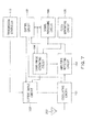
- Fig. 1 is a block structure diagram of an oscillator according to the embodiment.
- the oscillator in Fig. 1 comprises an antenna 202, an oscillating circuit 101, a current source circuit 103, an amplitude detecting circuit 102, a short pulse generating circuit 104, a clock circuit 105, a signal processing circuit 106 and a control circuit 107.
- the oscillating circuit 101 has a controllable oscillation frequency, and is given a power supply current from the current source circuit 103.
- the value of the power supply current is controlled such that when an input from the antenna 202 into the oscillating circuit 101 via an input terminal thereof is a no-signal state, the oscillating circuit 101 does not oscillate, and when a signal (received signal) having a desired power or more is input, the oscillating circuit 101 oscillates.
- the current value is controlled by the control circuit 107.
- the oscillation frequency of the oscillating circuit 101 is also adjusted under control of the control circuit 107. The oscillation frequency is adjusted so as to be tuned to an external reference input signal.
- the clock circuit 105 generates a low frequency clock signal (see Fig. 4(A) described later).
- the short pulse generating circuit 104 detects an edge of the low frequency clock signal, and generates a sufficiently shorter pulse than a clock wavelength (see Fig. 4(B) described later).
- the short pulse generating circuit 104 inputs the short pulse signal into the current source circuit 103. Only when being input with the pulse signal, the current source circuit 103 generates a power supply current and inputs it into the oscillating circuit 101. Thereby, only when a short pulse is input into the current source circuit 103, the power supply current is input into the oscillating circuit 101. When a radio signal is not input from the antenna 202 during the power supply current input, the oscillating circuit 101 does not oscillate and a consumed current is also less. When a radio signal which is at a desired input signal power or more and has substantially the same oscillation frequency is input from the antenna 202, the oscillating circuit 101 oscillates.
- the amplitude detecting circuit 102 detects an amplitude of the oscillation signal based on a reference value, and generates a binary (high/low) signal (demodulation signal).
- the signal processing circuit 106 determines a content (pattern) of the demodulation signal. When it is determined that the demodulation signal matches with a desired signal, the signal processing circuit 106 outputs a control signal to an external device.
- the control signal is a signal for powering on or off the external device, for example.
- Fig. 2 shows the structure of the oscillator of Fig. 1 in detail.
- the control circuit 107 in Fig. 1 is divided into a first control circuit 107a and a second control circuit 107b.
- the inside of the oscillating circuit 101 is configured of positive feedback transistors 301, 302, input transistors (a signal input buffer circuit) 303, 304, inductors 305, 306, and a capacitor 307.
- the positive feedback transistors 301 and 302 have a complementary structure. Since a signal having the same phase of a drain terminal is input into a gate terminal, respectively, a vibration is amplified.
- the inductors 305, 306 and the capacitor 307 form a resonance circuit, and a resonance frequency signal is input therein so that the vibration keeps.
- the oscillator is configured of the circuits.
- a radio signal from the antenna 202 is subjected to impedance matching and single-phase/differential conversion in a matching circuit 201, and a differential electric signal is input into the oscillating circuit 101.
- the input transistors 303 and 304 input the differential electric signal inside the oscillating circuit 101.
- the oscillation frequency is adjusted by the second control circuit 107b as follows. While an external reference input signal is being input, the capacity value of the capacitor 307 is adjusted by the second control circuit 107b, and the inductors 305, 306 and the resonance frequency are adjusted. The value of the capacitor 307 is fixed where the oscillation amplitude detected by the amplitude detecting circuit 102 is maximum.
- the oscillation level is adjusted by the first control circuit 107a as follows. While the input into the oscillating circuit 101 is in a no-signal input state, the power supply current of the current source circuit 103 is increased from zero in a stepwise manner by the first control circuit 107a. As the current increases, the oscillating circuit 101 starts oscillating at a certain current. The oscillation amplitude is detected by the amplitude detecting circuit 102 and is notified to the first control circuit 107a. The first control circuit 107a stores the current value at which oscillation does not occur. For example, the power supply current value m (m is an integer of 1 or more) stages before the power supply current where oscillation occurs is stored.
- the control circuit 107 detects and stores the power supply current value at which oscillation does not occur in a no-signal input state and oscillation occurs when a signal having a predetermined input power is input.
- the oscillation level adjustment will be described below in detail.
- Fig. 3 shows a control sequence of the oscillator according to the present embodiment.
- the oscillator enters the power supply ON state (S1), then the oscillation frequency of the oscillating circuit 101 is adjusted (S2), and then the current value of the current source circuit 103 is adjusted (S3).
- the oscillator enters a signal waiting state, and waits for a radio signal to be input (S4).
- step S2 when a predetermined period has elapsed in a timer or an event such as change in temperature has occurred, the processing returns to step S2 to adjust the oscillation frequency or to adjust the current value again. This is because the oscillation frequency or the power supply current value for oscillation is shifted depending on the temperature or the state of voltage system.
- a signal detection processing (S5) is performed. That is, an oscillation frequency signal is extracted by the oscillating circuit 101 and a binary signal (demodulation signal) is generated by the amplitude detecting circuit 102 based on the extracted signal.
- the signal processing circuit 106 determines whether the demodulation signal corresponds to a desired one. When the signal is not desired, the processing returns to the signal waiting in step S4.
- the signal processing circuit 106 When the demodulation signal is desired, the signal processing circuit 106 outputs a control signal for an external device or the like. For example, a control signal for switching the main power supply of the external device from OFF to ON is output. Thereafter, the oscillator is powered off.
- Figs. 4(A) to 4(E) show the operation timing charts of a clock signal, a short pulse signal, a RF (Radio Frequency) signal, an oscillator's oscillation signal and a received signal, respectively.
- a clock signal a short pulse signal
- a RF (Radio Frequency) signal an oscillator's oscillation signal and a received signal, respectively.
- the period of the clock signal is sufficiently longer than that of the RF signal received at the antenna 202, and is sufficiently shorter than the basic period of the data rate of data on the RF signal ( Fig. 4(A) ).
- the short pulse signal is generated by detecting an edge of the clock signal as a pulse signal, and has a sufficiently shorter pulse width than the clock wavelength ( Fig. 4(B) ).
- the clock period is 100 us and the pulse width of the short pulse is 1 us.
- the power supply current is supplied to the oscillating circuit 101 according to the pulse width of the short pulse. Thereby, the duty ratio of the current is 1/100 and a consumed power is reduced.
- the short pulse is generated at an edge rising timing in the example of Fig. 4(B)
- the short pulse may be generated at a timing offset from the rising edge (for example, in the middle between the rising edge and the falling edge).
- the RF signal is a low data rate signal on a high frequency carrier wave, and is delivered with on/off keying ( Fig. 4(C) ).
- the RF signal is a microwave in 2.45 GHz band and its data rate is 1 kb/s, the basic period is 1000 us.
- the oscillating circuit 101 reacts to the RF signal to be in an oscillation state, and outputs an oscillation signal ( Fig. 4(D) ).
- the RF signal is off, the oscillator remains in a steady state with no vibration ( Fig. 4(D) ).
- the oscillation and the steady state are detected and the presence of the on/off keying signal is determined by the amplitude detecting circuit 102 ( Fig. 4(E) ).
- Fig. 5 shows a sequence of current adjustment.
- the horizontal axis indicates time and the vertical axis indicates the value of the power supply current of the oscillating circuit 101.
- the amount of supplied current to the oscillating circuit 10 is increased step by step over time according to the short pulse shown in Fig. 4(B) .
- a RF input part of the oscillating circuit 101 performs a processing such as grounding to prevent an external noise from being input.
- a current at which oscillation does not occur is initially supplied and a current is gradually increased, and when a current exceeding an oscillation threshold in the Figure is supplied, the oscillator starts self-oscillating.
- the state is stored and the current value is returned to a current value m (m is an integer of 1 or more) stages before the step. In the Figure, the current value returns two stages before. Assuming that this state is a current setting value, the steady state with no vibration remains during no signal, and when a weak RF signal is input, oscillation starts.
- Fig. 6 is a block diagram of a radio device mounting thereon the oscillator according to the present embodiment.
- a Tx part 407 and an Rx part 406 are a transmitter and a receiver of the radio device, respectively.
- An oscillator 401 is provided independently from the transmitter and the receiver. It waits for a signal from an antenna 402 via a switch 405. There is a path for inputting a reference frequency signal from the Tx part 407 via a switch 404 into the oscillator 401.
- the reference frequency signal corresponds to the external reference input signal and is used for adjusting the oscillation frequency.
- a transformer 403 is provided between the switches 404, 405 and the antenna 402.
- a signal processing circuit 408 processes transmission/received signals in the Tx part 407 and the Rx part 406.
- the Tx part 407 and the Rx part 406 are powered off and only the oscillator 401 waits for a signal.
- the oscillator 401 receives a desired radio signal, the oscillator 401 outputs a control signal for turning on the power supplies of the Tx part 407 and the Rx part 406 so that the Tx part 407 and the Rx part 406 are powered on.
- the switch 405 is switched from the oscillator 401 to the Rx part 406 and the switch 404 is switched from the oscillator 401 to the transformer 403.
- the oscillator according to the present embodiment is used in this way so that lowered power consumption is achieved while a signal is always being waited during signal waiting.
- a signal waiting circuit with high sensitivity and super-low power consumption can be provided.
- Fig. 7 is a block diagram when the oscillating circuit is used for transmission.
- a transmission controller 110 is added to the constituents of Fig. 1 .
- the constituents having the same names as those in Fig. 1 are denoted with the same reference numerals, and a repeated explanation thereof will be omitted except for extended processings.
- the transmission controller 110 controls a power supply current to an oscillating circuit 101 when transmitting a transmission signal. Assuming a modulation system of the transmission signal as on/off keying, the transmission controller 110 controls the power supply circuit 103 such that a current at a current level where self-oscillation is possible can keep being supplied to the oscillating circuit 101 during an ON signal transmitting time. During an OFF signal, the power supply circuit 103 is controlled such that a current supply to the oscillating circuit 101 is stopped. The oscillator is oscillated according to the transmission signal in this way, thereby transmitting the signal.
- a transmitting circuit with high sensitivity and super-low power consumption can be provided.
- Fig. 8 is a block diagram of a radio communication circuit control system (radio communication device) using the oscillator according to the present embodiment.
- a startup signal detecting circuit 501 comprises an oscillator 502, a signal processing circuit 503, and power supply switches 504, 505.
- a radio communication circuit 511 comprises a Tx part 514, an Rx part 513, a switch 512 and a signal processing circuit 515.
- a power supply 521 is directed for supplying a power to the startup signal detecting circuit 501 and the radio communication circuit 511.
- the power supply switch 505 is powered off to stop supplying a power to the radio communication circuit 511, and the power supply switch 504 is powered on to supply a power to the startup signal detecting circuit 501.
- the signal processing circuit 503 determines whether the radio signal is a desired signal, and when it is a desired signal, the power supply switch 505 is switched to ON. Thereafter, when radio communication is normally made in the radio communication circuit 511, a control signal for powering off the power supply switch 504 of the startup signal detecting circuit 501 is output from the signal processing circuit 515 and the signal processing circuit and the oscillator of the startup signal detecting circuit 501 is powered off until the radio communication circuit 511 terminates the communication.
- radio communication circuit 511 can be completely powered off during the signal waiting in the system using the oscillator according to the present embodiment, lowered power consumption can be achieved while always waiting for a signal.
Landscapes
- Engineering & Computer Science (AREA)
- Power Engineering (AREA)
- Inductance-Capacitance Distribution Constants And Capacitance-Resistance Oscillators (AREA)
- Transceivers (AREA)
Applications Claiming Priority (1)
| Application Number | Priority Date | Filing Date | Title |
|---|---|---|---|
| JP2011194283A JP5575073B2 (ja) | 2011-09-06 | 2011-09-06 | 発振装置および無線通信装置 |
Publications (3)
| Publication Number | Publication Date |
|---|---|
| EP2568607A2 true EP2568607A2 (de) | 2013-03-13 |
| EP2568607A3 EP2568607A3 (de) | 2013-04-17 |
| EP2568607B1 EP2568607B1 (de) | 2014-06-25 |
Family
ID=46507852
Family Applications (1)
| Application Number | Title | Priority Date | Filing Date |
|---|---|---|---|
| EP12172733.3A Not-in-force EP2568607B1 (de) | 2011-09-06 | 2012-06-20 | Oszillator und Funkkommunikationsvorrichtung |
Country Status (3)
| Country | Link |
|---|---|
| US (1) | US9515606B2 (de) |
| EP (1) | EP2568607B1 (de) |
| JP (1) | JP5575073B2 (de) |
Cited By (2)
| Publication number | Priority date | Publication date | Assignee | Title |
|---|---|---|---|---|
| EP3442129A1 (de) * | 2017-08-11 | 2019-02-13 | Samsung Electronics Co., Ltd. | Empfänger und empfangsverfahren auf basis von impuls |
| CN109391336A (zh) * | 2017-08-11 | 2019-02-26 | 三星电子株式会社 | 基于脉冲的接收方法和接收器 |
Families Citing this family (10)
| Publication number | Priority date | Publication date | Assignee | Title |
|---|---|---|---|---|
| EP2941797B1 (de) | 2012-12-03 | 2019-11-20 | Dockon AG | Rauscharmes detektionssystem mit einem log-detektor-verstärker |
| WO2014152307A1 (en) | 2013-03-15 | 2014-09-25 | Dockon Ag | Low-power, noise insensitive communication channel using logarithmic detector amplifier (lda) demodulator |
| WO2014144919A1 (en) | 2013-03-15 | 2014-09-18 | Forrest James Brown | Power combiner and fixed/adjustable cpl antennas |
| US9684807B2 (en) | 2013-03-15 | 2017-06-20 | Dockon Ag | Frequency selective logarithmic amplifier with intrinsic frequency demodulation capability |
| US9236892B2 (en) | 2013-03-15 | 2016-01-12 | Dockon Ag | Combination of steering antennas, CPL antenna(s), and one or more receive logarithmic detector amplifiers for SISO and MIMO applications |
| US11183974B2 (en) | 2013-09-12 | 2021-11-23 | Dockon Ag | Logarithmic detector amplifier system in open-loop configuration for use as high sensitivity selective receiver without frequency conversion |
| KR101884242B1 (ko) * | 2013-09-12 | 2018-08-01 | 도콘 아게 | 주파수 변환 없이 고감도 선택적 수신기로서 사용되기 위한 대수 검출 증폭기 시스템 |
| US11082014B2 (en) | 2013-09-12 | 2021-08-03 | Dockon Ag | Advanced amplifier system for ultra-wide band RF communication |
| US9781022B2 (en) * | 2014-04-18 | 2017-10-03 | Sital Technology Ltd. | Fault detection in communication system |
| US20200177126A1 (en) * | 2018-11-29 | 2020-06-04 | Qualcomm Incorporated | Wide tuning range oscillator |
Family Cites Families (16)
| Publication number | Priority date | Publication date | Assignee | Title |
|---|---|---|---|---|
| JPH10173567A (ja) * | 1996-12-12 | 1998-06-26 | Omron Corp | 受信機及びリモートコントロール装置 |
| JPH10256928A (ja) * | 1997-03-13 | 1998-09-25 | Omron Corp | 超再生受信装置、方法、リモコン受信器およびリモコンシステム |
| US6876181B1 (en) * | 1998-02-27 | 2005-04-05 | Power Integrations, Inc. | Off-line converter with digital control |
| GB2343571B (en) * | 1998-11-07 | 2001-01-10 | Marconi Electronic Syst Ltd | A receiver circuit |
| JP3652304B2 (ja) * | 2001-11-29 | 2005-05-25 | Necマイクロシステム株式会社 | クロック生成回路及びクロック生成方法 |
| JP2004247848A (ja) * | 2003-02-12 | 2004-09-02 | Renesas Technology Corp | 通信装置 |
| US7215936B2 (en) * | 2003-04-02 | 2007-05-08 | Bogdan Sadowski | Super-regenerative receiver including phase-locked loop |
| JP2006157630A (ja) * | 2004-11-30 | 2006-06-15 | Nec Electronics Corp | Pll回路 |
| JP4542978B2 (ja) * | 2005-10-27 | 2010-09-15 | パナソニック株式会社 | 電源電圧制御装置 |
| KR100665330B1 (ko) | 2005-12-19 | 2007-01-09 | 삼성전기주식회사 | 수퍼리제너레이티브 수신기 |
| US7826815B2 (en) * | 2007-07-13 | 2010-11-02 | Fairchild Semiconductor Corporation | Dynamic selection of oscillation signal frequency for power converter |
| JP4758483B2 (ja) * | 2009-01-15 | 2011-08-31 | シャープ株式会社 | 電子装置 |
| JP5590934B2 (ja) * | 2010-03-24 | 2014-09-17 | スパンション エルエルシー | スイッチング電源の制御回路及び電子機器 |
| US8390433B2 (en) * | 2010-04-09 | 2013-03-05 | Eigent Technologies Inc. | Method and system for low cost, power efficient, wireless transponder devices with enhanced functionality |
| EP2402721B1 (de) * | 2010-07-02 | 2016-08-10 | Stichting IMEC Nederland | Leistungsverwaltungssystem für drahtlose autonome Wandlerlösungen |
| JP5122622B2 (ja) * | 2010-09-24 | 2013-01-16 | シャープ株式会社 | スイッチング電源装置 |
-
2011
- 2011-09-06 JP JP2011194283A patent/JP5575073B2/ja not_active Expired - Fee Related
-
2012
- 2012-06-18 US US13/526,005 patent/US9515606B2/en not_active Expired - Fee Related
- 2012-06-20 EP EP12172733.3A patent/EP2568607B1/de not_active Not-in-force
Non-Patent Citations (1)
| Title |
|---|
| None |
Cited By (3)
| Publication number | Priority date | Publication date | Assignee | Title |
|---|---|---|---|---|
| EP3442129A1 (de) * | 2017-08-11 | 2019-02-13 | Samsung Electronics Co., Ltd. | Empfänger und empfangsverfahren auf basis von impuls |
| CN109391336A (zh) * | 2017-08-11 | 2019-02-26 | 三星电子株式会社 | 基于脉冲的接收方法和接收器 |
| US10554457B2 (en) | 2017-08-11 | 2020-02-04 | Samsung Electronics Co., Ltd. | Receiver and reception method based on pulse |
Also Published As
| Publication number | Publication date |
|---|---|
| JP2013055613A (ja) | 2013-03-21 |
| US9515606B2 (en) | 2016-12-06 |
| JP5575073B2 (ja) | 2014-08-20 |
| EP2568607B1 (de) | 2014-06-25 |
| EP2568607A3 (de) | 2013-04-17 |
| US20130059548A1 (en) | 2013-03-07 |
Similar Documents
| Publication | Publication Date | Title |
|---|---|---|
| US9515606B2 (en) | Oscillator and radio communication device | |
| KR100682000B1 (ko) | 무선 통신 시스템 | |
| US20100289591A1 (en) | System and method for efficiently generating an oscillating signal | |
| KR101975137B1 (ko) | 크리스탈 오실레이터 회로에 대한 시동 기간의 지속 시간 단축 | |
| US20090174454A1 (en) | Clock circuit for a microprocessor | |
| EP1402643B1 (de) | Abstimmbare spannungsgesteuerte oszillatorschaltung mit erfassungshilfe und verfahren zum betrieb derselben | |
| EP3139497B1 (de) | Oszillator mit günstigem startverhalten | |
| ATE527750T1 (de) | Hochfrequenzoszillationsgerät, funkgerät und radar | |
| WO2020237097A1 (en) | Multi-mode oscillation circuitry with stepping control | |
| KR101392955B1 (ko) | 발진 신호를 생성하기 위한 장치, 방법 및 컴퓨터-판독가능 매체, 그리고 이를 이용한 디바이스들 | |
| US9991849B2 (en) | Wireless communication device and power source device | |
| CN210297681U (zh) | 一种无线射频发射装置 | |
| CN102739266B (zh) | 一种基于数控振荡器的多模发射机 | |
| JP3094527B2 (ja) | 送信装置 | |
| KR100472597B1 (ko) | 송신출력 가변식 무선주파수 모듈 | |
| KR100435556B1 (ko) | Rf-모듈의 전원 인가장치 | |
| KR20010011832A (ko) | 트리플모드용 이동단말기의 송신회로에서의 중간주파수 발생장치 | |
| JP2008048026A (ja) | 通信装置の制御方法及び通信装置 | |
| JPH06120853A (ja) | 特定小電力無線用通信機 | |
| GB2414097B (en) | Communication device | |
| JP2018186415A (ja) | 無線通信装置 | |
| WO2001097393A1 (en) | Mobile wireless communication device | |
| KR20060062009A (ko) | 휴대용 단말기의 파워 앰프 시스템 |
Legal Events
| Date | Code | Title | Description |
|---|---|---|---|
| PUAI | Public reference made under article 153(3) epc to a published international application that has entered the european phase |
Free format text: ORIGINAL CODE: 0009012 |
|
| 17P | Request for examination filed |
Effective date: 20120620 |
|
| AK | Designated contracting states |
Kind code of ref document: A2 Designated state(s): AL AT BE BG CH CY CZ DE DK EE ES FI FR GB GR HR HU IE IS IT LI LT LU LV MC MK MT NL NO PL PT RO RS SE SI SK SM TR |
|
| AX | Request for extension of the european patent |
Extension state: BA ME |
|
| PUAL | Search report despatched |
Free format text: ORIGINAL CODE: 0009013 |
|
| AK | Designated contracting states |
Kind code of ref document: A3 Designated state(s): AL AT BE BG CH CY CZ DE DK EE ES FI FR GB GR HR HU IE IS IT LI LT LU LV MC MK MT NL NO PL PT RO RS SE SI SK SM TR |
|
| AX | Request for extension of the european patent |
Extension state: BA ME |
|
| RIC1 | Information provided on ipc code assigned before grant |
Ipc: H03L 3/00 20060101AFI20130308BHEP Ipc: H04B 1/30 20060101ALI20130308BHEP Ipc: H03D 11/02 20060101ALI20130308BHEP |
|
| RIC1 | Information provided on ipc code assigned before grant |
Ipc: H03D 11/02 20060101ALI20131218BHEP Ipc: H03B 5/12 20060101ALI20131218BHEP Ipc: H03L 3/00 20060101AFI20131218BHEP Ipc: H04B 1/30 20060101ALI20131218BHEP |
|
| GRAP | Despatch of communication of intention to grant a patent |
Free format text: ORIGINAL CODE: EPIDOSNIGR1 |
|
| INTG | Intention to grant announced |
Effective date: 20140207 |
|
| GRAS | Grant fee paid |
Free format text: ORIGINAL CODE: EPIDOSNIGR3 |
|
| GRAA | (expected) grant |
Free format text: ORIGINAL CODE: 0009210 |
|
| AK | Designated contracting states |
Kind code of ref document: B1 Designated state(s): AL AT BE BG CH CY CZ DE DK EE ES FI FR GB GR HR HU IE IS IT LI LT LU LV MC MK MT NL NO PL PT RO RS SE SI SK SM TR |
|
| REG | Reference to a national code |
Ref country code: GB Ref legal event code: FG4D |
|
| REG | Reference to a national code |
Ref country code: CH Ref legal event code: EP |
|
| REG | Reference to a national code |
Ref country code: AT Ref legal event code: REF Ref document number: 675226 Country of ref document: AT Kind code of ref document: T Effective date: 20140715 |
|
| REG | Reference to a national code |
Ref country code: IE Ref legal event code: FG4D |
|
| REG | Reference to a national code |
Ref country code: DE Ref legal event code: R096 Ref document number: 602012002197 Country of ref document: DE Effective date: 20140807 |
|
| REG | Reference to a national code |
Ref country code: NL Ref legal event code: T3 |
|
| PG25 | Lapsed in a contracting state [announced via postgrant information from national office to epo] |
Ref country code: NO Free format text: LAPSE BECAUSE OF FAILURE TO SUBMIT A TRANSLATION OF THE DESCRIPTION OR TO PAY THE FEE WITHIN THE PRESCRIBED TIME-LIMIT Effective date: 20140925 Ref country code: GR Free format text: LAPSE BECAUSE OF FAILURE TO SUBMIT A TRANSLATION OF THE DESCRIPTION OR TO PAY THE FEE WITHIN THE PRESCRIBED TIME-LIMIT Effective date: 20140926 Ref country code: CY Free format text: LAPSE BECAUSE OF FAILURE TO SUBMIT A TRANSLATION OF THE DESCRIPTION OR TO PAY THE FEE WITHIN THE PRESCRIBED TIME-LIMIT Effective date: 20140625 Ref country code: LT Free format text: LAPSE BECAUSE OF FAILURE TO SUBMIT A TRANSLATION OF THE DESCRIPTION OR TO PAY THE FEE WITHIN THE PRESCRIBED TIME-LIMIT Effective date: 20140625 Ref country code: FI Free format text: LAPSE BECAUSE OF FAILURE TO SUBMIT A TRANSLATION OF THE DESCRIPTION OR TO PAY THE FEE WITHIN THE PRESCRIBED TIME-LIMIT Effective date: 20140625 |
|
| REG | Reference to a national code |
Ref country code: AT Ref legal event code: MK05 Ref document number: 675226 Country of ref document: AT Kind code of ref document: T Effective date: 20140625 |
|
| REG | Reference to a national code |
Ref country code: LT Ref legal event code: MG4D |
|
| PG25 | Lapsed in a contracting state [announced via postgrant information from national office to epo] |
Ref country code: RS Free format text: LAPSE BECAUSE OF FAILURE TO SUBMIT A TRANSLATION OF THE DESCRIPTION OR TO PAY THE FEE WITHIN THE PRESCRIBED TIME-LIMIT Effective date: 20140625 Ref country code: LV Free format text: LAPSE BECAUSE OF FAILURE TO SUBMIT A TRANSLATION OF THE DESCRIPTION OR TO PAY THE FEE WITHIN THE PRESCRIBED TIME-LIMIT Effective date: 20140625 Ref country code: SE Free format text: LAPSE BECAUSE OF FAILURE TO SUBMIT A TRANSLATION OF THE DESCRIPTION OR TO PAY THE FEE WITHIN THE PRESCRIBED TIME-LIMIT Effective date: 20140625 Ref country code: HR Free format text: LAPSE BECAUSE OF FAILURE TO SUBMIT A TRANSLATION OF THE DESCRIPTION OR TO PAY THE FEE WITHIN THE PRESCRIBED TIME-LIMIT Effective date: 20140625 |
|
| PG25 | Lapsed in a contracting state [announced via postgrant information from national office to epo] |
Ref country code: RO Free format text: LAPSE BECAUSE OF FAILURE TO SUBMIT A TRANSLATION OF THE DESCRIPTION OR TO PAY THE FEE WITHIN THE PRESCRIBED TIME-LIMIT Effective date: 20140625 Ref country code: PT Free format text: LAPSE BECAUSE OF FAILURE TO SUBMIT A TRANSLATION OF THE DESCRIPTION OR TO PAY THE FEE WITHIN THE PRESCRIBED TIME-LIMIT Effective date: 20141027 Ref country code: SK Free format text: LAPSE BECAUSE OF FAILURE TO SUBMIT A TRANSLATION OF THE DESCRIPTION OR TO PAY THE FEE WITHIN THE PRESCRIBED TIME-LIMIT Effective date: 20140625 Ref country code: EE Free format text: LAPSE BECAUSE OF FAILURE TO SUBMIT A TRANSLATION OF THE DESCRIPTION OR TO PAY THE FEE WITHIN THE PRESCRIBED TIME-LIMIT Effective date: 20140625 Ref country code: CZ Free format text: LAPSE BECAUSE OF FAILURE TO SUBMIT A TRANSLATION OF THE DESCRIPTION OR TO PAY THE FEE WITHIN THE PRESCRIBED TIME-LIMIT Effective date: 20140625 Ref country code: ES Free format text: LAPSE BECAUSE OF FAILURE TO SUBMIT A TRANSLATION OF THE DESCRIPTION OR TO PAY THE FEE WITHIN THE PRESCRIBED TIME-LIMIT Effective date: 20140625 |
|
| PG25 | Lapsed in a contracting state [announced via postgrant information from national office to epo] |
Ref country code: PL Free format text: LAPSE BECAUSE OF FAILURE TO SUBMIT A TRANSLATION OF THE DESCRIPTION OR TO PAY THE FEE WITHIN THE PRESCRIBED TIME-LIMIT Effective date: 20140625 Ref country code: AT Free format text: LAPSE BECAUSE OF FAILURE TO SUBMIT A TRANSLATION OF THE DESCRIPTION OR TO PAY THE FEE WITHIN THE PRESCRIBED TIME-LIMIT Effective date: 20140625 Ref country code: IS Free format text: LAPSE BECAUSE OF FAILURE TO SUBMIT A TRANSLATION OF THE DESCRIPTION OR TO PAY THE FEE WITHIN THE PRESCRIBED TIME-LIMIT Effective date: 20141025 |
|
| REG | Reference to a national code |
Ref country code: DE Ref legal event code: R097 Ref document number: 602012002197 Country of ref document: DE |
|
| PG25 | Lapsed in a contracting state [announced via postgrant information from national office to epo] |
Ref country code: IT Free format text: LAPSE BECAUSE OF FAILURE TO SUBMIT A TRANSLATION OF THE DESCRIPTION OR TO PAY THE FEE WITHIN THE PRESCRIBED TIME-LIMIT Effective date: 20140625 Ref country code: DK Free format text: LAPSE BECAUSE OF FAILURE TO SUBMIT A TRANSLATION OF THE DESCRIPTION OR TO PAY THE FEE WITHIN THE PRESCRIBED TIME-LIMIT Effective date: 20140625 |
|
| PLBE | No opposition filed within time limit |
Free format text: ORIGINAL CODE: 0009261 |
|
| STAA | Information on the status of an ep patent application or granted ep patent |
Free format text: STATUS: NO OPPOSITION FILED WITHIN TIME LIMIT |
|
| 26N | No opposition filed |
Effective date: 20150326 |
|
| PG25 | Lapsed in a contracting state [announced via postgrant information from national office to epo] |
Ref country code: BE Free format text: LAPSE BECAUSE OF FAILURE TO SUBMIT A TRANSLATION OF THE DESCRIPTION OR TO PAY THE FEE WITHIN THE PRESCRIBED TIME-LIMIT Effective date: 20140625 |
|
| PG25 | Lapsed in a contracting state [announced via postgrant information from national office to epo] |
Ref country code: SI Free format text: LAPSE BECAUSE OF FAILURE TO SUBMIT A TRANSLATION OF THE DESCRIPTION OR TO PAY THE FEE WITHIN THE PRESCRIBED TIME-LIMIT Effective date: 20140625 |
|
| PG25 | Lapsed in a contracting state [announced via postgrant information from national office to epo] |
Ref country code: MC Free format text: LAPSE BECAUSE OF FAILURE TO SUBMIT A TRANSLATION OF THE DESCRIPTION OR TO PAY THE FEE WITHIN THE PRESCRIBED TIME-LIMIT Effective date: 20140625 |
|
| REG | Reference to a national code |
Ref country code: CH Ref legal event code: PL |
|
| PG25 | Lapsed in a contracting state [announced via postgrant information from national office to epo] |
Ref country code: LU Free format text: LAPSE BECAUSE OF FAILURE TO SUBMIT A TRANSLATION OF THE DESCRIPTION OR TO PAY THE FEE WITHIN THE PRESCRIBED TIME-LIMIT Effective date: 20150620 |
|
| REG | Reference to a national code |
Ref country code: IE Ref legal event code: MM4A |
|
| PG25 | Lapsed in a contracting state [announced via postgrant information from national office to epo] |
Ref country code: IE Free format text: LAPSE BECAUSE OF NON-PAYMENT OF DUE FEES Effective date: 20150620 Ref country code: LI Free format text: LAPSE BECAUSE OF NON-PAYMENT OF DUE FEES Effective date: 20150630 Ref country code: CH Free format text: LAPSE BECAUSE OF NON-PAYMENT OF DUE FEES Effective date: 20150630 |
|
| REG | Reference to a national code |
Ref country code: FR Ref legal event code: PLFP Year of fee payment: 5 |
|
| PG25 | Lapsed in a contracting state [announced via postgrant information from national office to epo] |
Ref country code: MT Free format text: LAPSE BECAUSE OF FAILURE TO SUBMIT A TRANSLATION OF THE DESCRIPTION OR TO PAY THE FEE WITHIN THE PRESCRIBED TIME-LIMIT Effective date: 20140625 |
|
| REG | Reference to a national code |
Ref country code: FR Ref legal event code: PLFP Year of fee payment: 6 |
|
| PG25 | Lapsed in a contracting state [announced via postgrant information from national office to epo] |
Ref country code: HU Free format text: LAPSE BECAUSE OF FAILURE TO SUBMIT A TRANSLATION OF THE DESCRIPTION OR TO PAY THE FEE WITHIN THE PRESCRIBED TIME-LIMIT; INVALID AB INITIO Effective date: 20120620 |
|
| PG25 | Lapsed in a contracting state [announced via postgrant information from national office to epo] |
Ref country code: BG Free format text: LAPSE BECAUSE OF EXPIRATION OF PROTECTION Effective date: 20150630 |
|
| PG25 | Lapsed in a contracting state [announced via postgrant information from national office to epo] |
Ref country code: SM Free format text: LAPSE BECAUSE OF FAILURE TO SUBMIT A TRANSLATION OF THE DESCRIPTION OR TO PAY THE FEE WITHIN THE PRESCRIBED TIME-LIMIT Effective date: 20140625 |
|
| PG25 | Lapsed in a contracting state [announced via postgrant information from national office to epo] |
Ref country code: TR Free format text: LAPSE BECAUSE OF FAILURE TO SUBMIT A TRANSLATION OF THE DESCRIPTION OR TO PAY THE FEE WITHIN THE PRESCRIBED TIME-LIMIT Effective date: 20140625 |
|
| REG | Reference to a national code |
Ref country code: FR Ref legal event code: PLFP Year of fee payment: 7 |
|
| PG25 | Lapsed in a contracting state [announced via postgrant information from national office to epo] |
Ref country code: MK Free format text: LAPSE BECAUSE OF FAILURE TO SUBMIT A TRANSLATION OF THE DESCRIPTION OR TO PAY THE FEE WITHIN THE PRESCRIBED TIME-LIMIT Effective date: 20140625 |
|
| PG25 | Lapsed in a contracting state [announced via postgrant information from national office to epo] |
Ref country code: AL Free format text: LAPSE BECAUSE OF FAILURE TO SUBMIT A TRANSLATION OF THE DESCRIPTION OR TO PAY THE FEE WITHIN THE PRESCRIBED TIME-LIMIT Effective date: 20140625 |
|
| PGFP | Annual fee paid to national office [announced via postgrant information from national office to epo] |
Ref country code: DE Payment date: 20210525 Year of fee payment: 10 Ref country code: NL Payment date: 20210615 Year of fee payment: 10 Ref country code: FR Payment date: 20210513 Year of fee payment: 10 |
|
| PGFP | Annual fee paid to national office [announced via postgrant information from national office to epo] |
Ref country code: GB Payment date: 20210526 Year of fee payment: 10 |
|
| REG | Reference to a national code |
Ref country code: DE Ref legal event code: R119 Ref document number: 602012002197 Country of ref document: DE |
|
| REG | Reference to a national code |
Ref country code: NL Ref legal event code: MM Effective date: 20220701 |
|
| GBPC | Gb: european patent ceased through non-payment of renewal fee |
Effective date: 20220620 |
|
| PG25 | Lapsed in a contracting state [announced via postgrant information from national office to epo] |
Ref country code: NL Free format text: LAPSE BECAUSE OF NON-PAYMENT OF DUE FEES Effective date: 20220701 |
|
| PG25 | Lapsed in a contracting state [announced via postgrant information from national office to epo] |
Ref country code: FR Free format text: LAPSE BECAUSE OF NON-PAYMENT OF DUE FEES Effective date: 20220630 |
|
| PG25 | Lapsed in a contracting state [announced via postgrant information from national office to epo] |
Ref country code: GB Free format text: LAPSE BECAUSE OF NON-PAYMENT OF DUE FEES Effective date: 20220620 Ref country code: DE Free format text: LAPSE BECAUSE OF NON-PAYMENT OF DUE FEES Effective date: 20230103 |