EP3442129A1 - Empfänger und empfangsverfahren auf basis von impuls - Google Patents
Empfänger und empfangsverfahren auf basis von impuls Download PDFInfo
- Publication number
- EP3442129A1 EP3442129A1 EP18186333.3A EP18186333A EP3442129A1 EP 3442129 A1 EP3442129 A1 EP 3442129A1 EP 18186333 A EP18186333 A EP 18186333A EP 3442129 A1 EP3442129 A1 EP 3442129A1
- Authority
- EP
- European Patent Office
- Prior art keywords
- pulse
- oscillation
- signal
- time
- radio signal
- Prior art date
- Legal status (The legal status is an assumption and is not a legal conclusion. Google has not performed a legal analysis and makes no representation as to the accuracy of the status listed.)
- Granted
Links
Images


Classifications
-
- H—ELECTRICITY
- H04—ELECTRIC COMMUNICATION TECHNIQUE
- H04L—TRANSMISSION OF DIGITAL INFORMATION, e.g. TELEGRAPHIC COMMUNICATION
- H04L27/00—Modulated-carrier systems
- H04L27/02—Amplitude-modulated carrier systems, e.g. using on-off keying; Single sideband or vestigial sideband modulation
- H04L27/06—Demodulator circuits; Receiver circuits
-
- H—ELECTRICITY
- H04—ELECTRIC COMMUNICATION TECHNIQUE
- H04B—TRANSMISSION
- H04B17/00—Monitoring; Testing
- H04B17/20—Monitoring; Testing of receivers
-
- H—ELECTRICITY
- H04—ELECTRIC COMMUNICATION TECHNIQUE
- H04B—TRANSMISSION
- H04B1/00—Details of transmission systems, not covered by a single one of groups H04B3/00 - H04B13/00; Details of transmission systems not characterised by the medium used for transmission
- H04B1/06—Receivers
- H04B1/16—Circuits
-
- H—ELECTRICITY
- H04—ELECTRIC COMMUNICATION TECHNIQUE
- H04B—TRANSMISSION
- H04B17/00—Monitoring; Testing
Definitions
- the following description relates to a receiver and a reception method based on a pulse.
- the loT device may be a subminiature wireless transceiver configured to perform communication at a low power to process information by performing transmission and reception of the information between distributed elements such as objects.
- wireless communication needs to be performed with a low power, a high receive sensitivity, and no latency.
- a receiver in one general aspect, includes an antenna configured to receive a radio signal; a pulse generator configured to generate a pulse; an oscillator configured to be driven based on the pulse to generate an oscillation signal based on the radio signal; and a measurer configured to be driven based on the pulse to measure an oscillation degree of the oscillation signal, wherein the radio signal is received based on the oscillation degree of the oscillation signal.
- the measurer may be further configured to measure an oscillation time of the oscillation signal as the oscillation degree of the oscillation signal, and the radio signal may be received based on the oscillation time of the oscillation signal.
- the measurer may be further configured to generate an output proportional to the oscillation time of the oscillation signal, and the radio signal may be received based on whether the generated output is greater than a threshold.
- the radio signal may be received as a first value in response to the oscillation time being greater than or equal to a threshold time, and received as a second value different from the first value in response to the oscillation time being less than the threshold time.
- An amplitude or a frequency of the radio signal received by the antenna may be received based on the oscillation time of the oscillation signal.
- An current supplier may be further configured to provide a first current to the oscillator in a first period of time from a start point in time of the pulse to an intermediate point in time between the start point in time of the pulse and an end point in time of the pulse, and provide a second current smaller than the first current to the oscillator in a second period of time from the intermediate point in time to the end point in time of the pulse.
- the oscillator may include a tank circuit including a plurality of capacitors, and the plurality of capacitors may have unequal values in a first period of time from a start point in time of the pulse to an intermediate point in time between the start point in time of the pulse and an end point in time of the pulse, and equal values in a second period of time from the intermediate point in time to the end point in time of the pulse.
- the receiver may further include an inductor having a Q-value greater than a threshold applied to the oscillator.
- the measurer may be further configured to generate an output proportional to an oscillation time of the oscillator, and the pulse generator may be further configured to adjust a width of the pulse based on the output generated by the measurer.
- the measurer may be further configured to generate an output proportional to an oscillation frequency of the oscillation signal and a width of the pulse based on an oscillation time of the oscillation signal.
- the pulse generator may be further configured to generate the pulse at an interval of a period less than 1/2 times an on-off keying (OOK) modulation period of the radio signal.
- OOK on-off keying
- the measurer may be further configured to detect an envelope of the oscillation signal as the oscillation degree of the oscillation signal, and the radio signal may be received based on the envelope of the oscillation signal,
- the measurer may be further configured to measure an amplitude of the detected envelope of the oscillation signal, and the radio signal is received based on whether the amplitude of the detected envelope is greater than a threshold.
- the oscillator and the measurer may be further configured to operate during an interval in which the oscillator and the measurer receive the pulse from the pulse generator.
- a power consumption of the receiver may be determined by a data rate of the radio signal and a width of the pulse.
- the receiver may further include a radio frequency (RF) amplifier configured to be driven based on the pulse to amplify the oscillation signal and output the amplified oscillation signal to the measurer.
- RF radio frequency
- a reception method includes generating a pulse at an interval of a predetermined period; generating, during the pulse, an oscillation signal based on a radio signal received by an antenna, the generating being enabled based on the pulse; and measuring, during the pulse, an oscillation degree of the oscillation signal, the measuring being enabled based on the pulse, wherein the radio signal is received based on the oscillation degree of the oscillation signal.
- the measuring may include generating an output proportional to an oscillation time of the oscillation signal as the oscillation degree of the oscillation signal, and the radio signal may be received based on whether the generated output is greater than a threshold.
- the measuring may include detecting an envelope of the oscillation signal as the oscillation degree of the oscillation signal, and the radio signal may be received based on whether an amplitude of the detected envelope is greater than a threshold.
- a non-transitory computer-readable medium stores instructions that, when executed by a processor, control the processor to perform the reception method described above.
- a receiver in another general aspect, includes an antenna configured to receive a radio signal; a pulse generator configured to generate a pulse at an interval of a predetermined period; an oscillator configured to be powered on by the pulse to generate an oscillation signal based on the radio signal only while the pulse is present; and a measurer configured to be powered on by the pulse to measure a parameter of the oscillation signal depending on the radio signal only while the pulse is present, wherein the radio signal is received based on the parameter of the oscillation signal.
- the measurer may be further configured to measure an oscillation time as the parameter of the oscillation signal or detect an envelope of the oscillation signal as the parameter of the oscillation signal, and the radio signal may be received based on the oscillation time of the oscillation signal or the envelope of the oscillation signal.
- the receiver may further include a fast startup circuit configured to reduce a startup time of the oscillator during a first portion of the pulse by either one or both of increasing a current supplied to the oscillator during the first portion of the pulse, and adjusting a value of a capacitor applied to the oscillator during the first portion of the pulse.
- a fast startup circuit configured to reduce a startup time of the oscillator during a first portion of the pulse by either one or both of increasing a current supplied to the oscillator during the first portion of the pulse, and adjusting a value of a capacitor applied to the oscillator during the first portion of the pulse.
- the oscillator may be a first oscillator configured to generate a first clock signal having a first frequency and requiring a first power level to operate
- the receiver may further include a second oscillator configured to generate a second clock signal having a second frequency lower than the first frequency and requiring a second power level lower than the first power level to operate, and a selector configured to select one of the first clock signal and the second clock signal based on the radio signal
- the pulse generator may be further configured to generate the pulse at the interval of the predetermined period based on the selected one of the first clock signal and the second clock signal.
- the selector may be further configured to select the first clock signal in response to the first frequency being at least twice a frequency of the radio signal and the second frequency being less than twice the frequency of the radio signal, and select the second clock signal in response to both the first frequency and the second frequency being at least twice the frequency of the radio signal.
- first,” “second,” and “third” may be used herein to describe various members, components, regions, layers, or sections, these members, components, regions, layers, or sections are not to be limited by these terms. Rather, these terms are only used to distinguish one member, component, region, layer, or section from another member, component, region, layer, or section. Thus, a first member, component, region, layer, or section referred to in examples described herein may also be referred to as a second member, component, region, layer, or section without departing from the teachings of the examples.
- FIG. 1 illustrates an example of a receiver.
- a receiver 100 includes an antenna 110, a pulse generator 120, an oscillator 130, and a measurer 140.
- the receiver 100 is a device for receiving a radio signal.
- the receiver 100 may be implemented as, for example, a subminiature wireless transceiver such as, for example, a low power communication device, an Internet of things (loT) device, an implantable communication device, or a medical implant communications system (MICS).
- a subminiature wireless transceiver such as, for example, a low power communication device, an Internet of things (loT) device, an implantable communication device, or a medical implant communications system (MICS).
- LoT Internet of things
- MISIS medical implant communications system
- a radio signal is received by the antenna 110.
- the radio signal is a signal transmitted and received through wireless communication, for example, a radio frequency (RF) signal.
- the RF signal is a signal modulated by amplitude shift keying (ASK), for example, on-off keying (OOK).
- the RF signal is modulated by frequency shift keying (FSK).
- ASK amplitude shift keying
- OOK on-off keying
- FSK frequency shift keying
- the pulse generator 120 generates a pulse.
- the pulse generator 120 generates the pulse based on a predetermined period.
- the predetermined period is less than 1/2 times an OOK modulation period of a radio signal.
- the pulse generated in the pulse generator 120 is provided to the oscillator 130 and the measurer 140.
- the oscillator 130 may be an LC-VCO (inductor capacitor-voltage controlled oscillator) driven by the pulse.
- the oscillator 130 does not operate during an interval in which a pulse is not provided to the oscillator 130, and thus an oscillation signal is not generated in the oscillator 130.
- the oscillator 130 operates in an interval in which the pulse is provided to the oscillator 130, and thus an oscillation signal is generated based on a radio signal.
- the oscillator 130 operates in a relatively short interval in which the pulse is provided from the pulse generator 120, whereby a power consumption of the receiver 100 is effectively reduced.
- the oscillator 130 When the pulse is provided to the oscillator 130, the oscillator 130 generates an oscillation signal based on the radio signal received by the antenna 110. For example, a signal generated in the oscillator 130 based on a radio signal "1" received by the antenna 110 in the interval in which the pulse is provided is different from a signal generated in the oscillator 130 based on a radio signal "0" received by the antenna 110 in the interval in which the pulse is provided.
- the oscillator 130 determines whether an RF carrier is present and generates the oscillation signal based on a determination result.
- the oscillation signal will also be described in detail with reference to FIG. 2 .
- the measurer 140 measures an oscillation degree of the oscillation signal.
- the measurer 140 is also driven by the pulse.
- the measurer 140 is driven to measure the oscillation degree of the oscillation signal during the interval in which the pulse is provided from the pulse generator 120.
- the measurer 140 measures an oscillation time of the oscillation signal or an envelope of the oscillation signal as the oscillation degree of the oscillation signal.
- a radio signal is received based on the oscillation degree of the oscillation signal measured in the measurer 140. In one example, the radio signal is received based on an oscillation time of the oscillation signal measured in the measurer 140. In another example, the radio signal is received based on an envelope of the oscillation signal measured in the measurer 140.
- FIG. 2 illustrates an example of a receiver including a time-to-digital converter (TDC).
- TDC time-to-digital converter
- a receiver 200 includes an antenna 210, a clock generator 220, a pulse generator 230, an oscillator 240, and a TDC 250.
- the measurer 140 of FIG. 1 may correspond to the TDC 250.
- the receiver 200 receives a radio signal V RF based on an oscillation time of an oscillation signal V OSC measured using the TDC 250.
- the radio signal V RF is received by the antenna 210.
- the radio signal V RF is a signal modulated by OOK, and may correspond to "1" or "0".
- the clock generator 220 generates a clock signal and provides the clock signal to the pulse generator 230.
- the pulse generator 230 generates a pulse V PULSE at an interval of a predetermined period based on the received clock signal.
- the oscillator 240 and the TDC 250 are enabled, for example, powered on, by the pulse V PULSE .
- the oscillator 240 is, for example, an inductor-capacitor (LC) oscillator driven by the pulse V PULSE to generate an oscillation signal V OSC based on the radio signal V RF .
- the oscillator 240 generates the oscillation signal V OSC oscillating in a period of time varying based on the radio signal V RF . For example, when the radio signal V RF received by the antenna 210 is "1", the oscillator 240 generates the oscillation signal V OSC oscillating in a greater period of time than in a case in which the radio signal V RF received by the antenna 210 is "0".
- LC inductor-capacitor
- the oscillator 240 When the radio signal V RF received by the antenna 210 is "0", the oscillator 240 generates the oscillation signal Vosc oscillating in a lesser period of time than in a case in which the radio signal V RF received by the antenna 210 is "1".
- the TDC 250 measures an oscillation time of the oscillation signal Vosc and outputs an output count N OUT corresponding to the measured oscillation time.
- the TDC 250 generates the output count N OUT proportionally to the oscillation time of the oscillation signal V OSC .
- the TDC 250 generates the output count N OUT based on an oscillating start time of the oscillation signal V OSC .
- an amplitude of the oscillation signal Vosc is greater than a threshold amplitude, the TDC 250 recognizes that the oscillation signal V OSC oscillates, and thus generates the output count N OUT .
- the receiver 200 receives the radio signal V RF based on the output count N OUT of the TDC 250.
- the output count N OUT of the TDC 250 is greater than or equal to a threshold count N REF , the receiver 200 receives the radio signal V RF corresponding to "1".
- the output count N OUT of the TDC 250 is less than the threshold count N REF , the receiver 200 receives the radio signal V RF corresponding to "0".
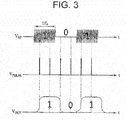
- FIGS. 3 through 6 illustrate an example of a procedure of receiving a radio signal in the receiver of FIG. 2 .
- FIG. 3 illustrates a radio signal V RF , a pulse V PULSE , and a received signal V OUT .
- the radio signal V RF is a signal modulated by OOK, and may correspond to "1" or "0".
- An OOK modulation period of the radio signal V RF is 1/fs.
- the pulse V PULSE is generated at a period less than or equal to 1/2 times 1/f s , which is the OOK modulation period of the radio signal V RF .
- f s is a data frequency or a data rate.
- the received signal V OUT corresponds to a value to which the radio signal V RF corresponds during an interval in which the pulse V PULSE is provided.
- the radio signal V RF corresponds to "1" at first, second, fifth, and sixth points in time at which a pulse is provided, and thus the received signal V OUT corresponds to "1" at the first, second, fifth, and sixth points in time.
- the radio signal V RF corresponds to "0" at third and fourth points in time in which a pulse is provided, and thus the received signal V OUT corresponds to "0" at the third and fourth points in time.
- a receiver operates based on the pulse V PULSE and measures an oscillation time of an oscillation signal using a TDC whereby the radio signal V RF is accurately received during a relatively short pulse period.
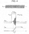
- the radio signal V RF corresponds to "1".
- the pulse V PULSE is high during T PULSE .
- the oscillation signal V OSC starts oscillating quickly in an oscillator. For example, the oscillation signal V OSC starts oscillating starting from a point in time relatively close to a rising edge of the pulse V PULSE .
- the oscillation signal V OSC starts oscillating quickly, an interval in which an amplitude of the oscillation signal V OSC is greater than or equal to a predetermined amplitude increases.
- a TDC measures a length of the interval in which the amplitude of the oscillation signal V OSC is greater than the predetermined amplitude. For example, an output count N OUT of the TDC is proportional to an oscillation time t 1 of the oscillation signal V OSC .
- a receiver receives the radio signal V RF corresponding to "1".
- the threshold time corresponds to a threshold count N REF .
- the output count N OUT of the TDC is greater than a threshold count N REF , it is determined that the oscillation time t 1 of the oscillation signal V OSC is greater than the threshold time.
- the radio signal V RF corresponds to "0".
- the oscillation signal Vosc starts oscillating slowly in the oscillator.
- the oscillation signal V OSC starts oscillating starting from a point in time relatively far from the rising edge of the pulse V PULSE .
- the interval in which the amplitude of the oscillation signal V OSC is greater than or equal to the predetermined amplitude decreases.
- the TDC continuously increases the output count N OUT starting from zero during the interval in which the amplitude of the oscillation signal V OSC is greater than the predetermined amplitude.
- the longer the interval in which the amplitude of the oscillation signal V OSC is greater than the predetermined amplitude the higher the output count N OUT .
- an oscillation time to of the oscillation signal V OSC is obtained based on the output count N OUT of the TDC.
- the receiver receives the radio signal V RF corresponding to "0".
- the threshold time corresponds to the threshold count N REF .
- the oscillation time to of the oscillation signal Vosc is less than the threshold time.
- the oscillation time to of the oscillation signal V OSC of FIG. 5 is less than the oscillation time t 1 of the oscillation signal V OSC in FIG. 4 .
- FIG. 6 illustrates an example of a procedure of receiving a radio signal using a TDC.
- the radio signal V RF is a signal modulated by OOK and corresponds to "1", “0", “1", and "0".
- An OOK modulation period of the radio signal V RF is T S , which corresponds to 1/f s shown in FIG. 3 .
- the pulse V PULSE is generated in a pulse generator at an interval of a predetermined period.
- the pulse V PULSE is generated at an interval of a predetermined period less than or equal to 1/2 times the OOK modulation period T S of the radio signal V RF .
- a receiver is powered on during an interval in which the pulse V PULSE is generated. Also, the receiver is powered off during an interval in which the pulse V PULSE is not generated.
- the interval in which the pulse V PULSE is generated has a length of T PULSE .
- an oscillator driven by the pulse V PULSE generates the oscillation signal V OSC based on the radio signal V RF .
- an oscillation time of the oscillation signal V OSC that is generated during an interval in which the radio signal V RF corresponds to "1" is greater than an oscillation time of the oscillation signal V OSC that is generated during an interval in which the radio signal V RF corresponds to "0".
- a TDC driven by the pulse V PULSE generates the output count N OUT proportionally to an oscillation time of the oscillation signal Vosc. For example, an oscillation time of the oscillation signal V OSC generated during the interval in which the radio signal V RF is "1" is greater than a threshold time. In this example, the output count N OUT of the TDC is greater than the threshold count N REF , and thus the receiver receives the radio signal V RF corresponding to "1". Also, an oscillation time of the oscillation signal V OSC generated during the interval in which the radio signal V RF is "0" is less than the threshold time. Thus, the output count N OUT of the TDC is less than the threshold count N REF , and thus the receiver receives the radio signal V RF corresponding to "0".
- the TDC continues to output the output count N OUT until a reset signal (not illustrated in FIG. 6 ) is input to the TDC to reset the output count N OUT to 0.
- the reset signal is input to the TDC before a pulse subsequent to the pulse V PULSE is generated to reset the output count N OUT to 0.
- the threshold count N REF may be predetermined or may be dynamically changed based on output counts N OUT of the TDC produced by a predetermined radio signal.
- a predetermined radio signal "1, 0, 1, 0" is input to the oscillator and causes the TDC to produce output counts N OUT "10, 5, 10, 5"
- the threshold count N REF is dynamically set to 7.5. That is, the threshold count N REF is dynamically set to a value halfway between the output count N OUT 10 produced by the radio signal "1" and the output count N OUT 5 produced by the radio signal "0.”.
- the predetermined radio signal "1, 0, 1, 0" may produce other output counts N OUT , or other predetermined radio signals may be used, or the threshold count N REF may be dynamically set using other schemes.
- FIG. 7 illustrates another example of a receiver including a TDC.
- a receiver 700 includes a controller 710, a receiving main block, for example, an RX main block 720, and an antenna 730.
- the receiver 700 is, for example, an RF transceiver.
- the controller 710 generates a pulse V PULSE and provides the pulse V PULSE to the RX main block 720.
- a resistor-capacitor (RC)-oscillator is a clock generator configured to generate a clock signal and provides a generated clock signal V RC to a pulse generator.
- the pulse generator generates a pulse V PULSE based on the clock signal V RC and provides the pulse V PULSE to an oscillator, an RF amplifier, for example, an operational amplifier, and a TDC in the RX main block 720.
- the pulse V PULSE is generated at an interval of a period determined by a frequency divider, and a width of the pulse V PULSE is determined by the pulse generator.
- a fast startup circuit is a circuit that enables an oscillation signal V OSC to be rapidly generated in an oscillator in order to reduce the width of the pulse V PULSE , will be described with reference to FIGS. 12 through 14 .
- the antenna 730 and a plurality of capacitors of a CAP bank form a tank circuit of the oscillator.
- the antenna 730 serves as an inductor of the tank circuit.
- the oscillator in the RX main block 720 is driven by the pulse V PULSE to generate the oscillation signal Vosc based on a radio signal received by the antenna 730.
- the oscillation signal Vosc is amplified by the RF amplifier.
- the RF amplifier is driven by the pulse V PULSE .
- FIG. 7 illustrates two RF amplifiers as one example, the RX main block 720 may include one RF amplifier or three or more RF amplifiers without restriction.
- the TDC outputs an output count N OUT that is proportional to an oscillation time of an amplified oscillation signal V OSC2 driven by the pulse V PULSE .
- the TDC receives a reset signal V RST from a reset controller, for example, an RST controller, and resets the output count N OUT before a pulse subsequent to the pulse V PULSE is provided.
- a synchronizer performs phase synchronization on a clock signal V SAM and the output count N OUT of the TDC. Also, a synchronized signal Vs is compared to a threshold voltage V REF in a comparator so that a received signal V OUT is output.
- the threshold voltage V REF corresponds to the aforementioned threshold count N REF .
- FIG. 8 illustrates an example of a procedure of receiving a radio signal in the receiver of FIG. 7 .
- FIG. 8 illustrates a radio signal V RF , a pulse V PULSE , an oscillation signal Vosc, amplified oscillation signals V OSC1 and V OSC2 , and an output count N OUT of a TDC.
- the radio signal V RF is "1" when the pulse V PULSE is generated.
- the receiver operates and receives and outputs the radio signal V RF .
- the receiver does not operate and continues to output a previously received signal.
- the pulse V PULSE is provided during a time T PULSE .
- the time T PULSE is greater than a startup time T SET .
- the startup time T SET will be described with reference to FIG. 9 .
- the oscillation signal Vosc is generated based on the radio signal V RF in an oscillator driven by the pulse V PULSE .
- the oscillation signal V OSC is amplified using at least one RF amplifier.
- V OSC1 and V OSC2 represent amplified oscillation signals.
- the TDC outputs an output count N OUT proportional to an oscillation time t 1 based on the amplified oscillation signal V OSC2 .
- the TDC outputs the output count N OUT proportional to the oscillation time t 1 by continuing to increment the output count N OUT as long as an amplitude of the amplified oscillation signal V OSC2 is greater than a threshold amplitude.
- the TDC continues to output the output count N OUT until a reset signal is input to the TDC.
- FIG. 9 illustrates an example of a procedure of generating an output of a TDC based on a radio signal.
- FIG. 9 illustrates a startup time T SET and an operation time T SS of a TDC.
- a receiver is powered on during an interval in which the pulse V PULSE is generated.
- the receiver operates based on impulse-based carrier sensing (IBCS) so that the receiver is powered on during an interval in which the pulse V PULSE is generated, and powered off during an interval in which the pulse V PULSE is not generated.
- IBCS impulse-based carrier sensing
- a width T PULSE of the pulse V PULSE is divided into the startup time T SET and the operation time Tss of the TDC.
- the startup time T SET is an interval in which an output is not generated in the TDC because an amplitude of an oscillation signal is less than or equal to a threshold amplitude.
- the operation time Tss is be an interval in which an output is generated in the TDC because the amplitude of the oscillation signal is greater than the threshold amplitude.
- the width T PULSE of the pulse V PULSE is expressed by Equation 1 below.
- T OSC denotes an oscillation period of an oscillator and f OSC denotes an oscillation frequency of the oscillator, where f OSC is a high frequency and may also be referred to as a carrier frequency.
- Equation 1 when the startup time T SET is reduced, or when the oscillation frequency f OSC increases, the width T PULSE of the pulse V PULSE is effectively reduced, and thus power consumption in the receiver is also reduced.
- T 1 represents a time measured in the TDC when the radio signal V RF is "1" and To represents a time measured in the TDC when the radio signal V RF is "0".
- the radio signal V RF is modulated by OOK.
- an output count N OUT of the TDC is proportional to the amplitude of the radio signal V RF so that the radio signal V RF is received without restrictions.
- the output count N OUT of the TDC is inversely proportional to a frequency difference between a frequency of the radio signal V RF and the oscillation frequency of the oscillation signal, whereby the radio signal V RF is received without restrictions.
- FIG. 10 illustrates an example of an output of a TDC that is not affected by jitter of a clock generator.
- FIG. 10 illustrates a radio signal V RF , a clock signal V RC generated in a clock generator, and a pulse V PULSE generated in a pulse generator.
- the clock signal V RC includes jitter.
- Jitter is a phenomenon in which a period of the clock generator generating the clock signal V RC deviates from its normal value.
- An oscillator generates the pulse V PULSE at a rising edge of the clock signal V RC .
- the jitter causes a pulse position fluctuation denoted by ⁇ T RC to appear at the rising edge of the clock signal V RC .
- a position fluctuation occurs in an output count N OUT of a TDC due to the pulse position fluctuation. Also, a point in time at which an output of the TDC is reset is changed based on a reset signal V RST .
- a receiver receives the radio signal V RF based on the output count N OUT of the TDC, and thus is not affected by the jitter of the clock generator.
- the output count N OUT of the TDC is proportional to a width of the pulse V PULSE and an oscillation frequency of an oscillation signal, and is not affected by the jitter of the clock generator.
- the receiver receives the radio signal V RF robustly despite the jitter of the clock generator therein.
- FIG. 11 illustrates an example of a TDC output change based on a change in a width of a pulse.
- FIG. 11 illustrates a pulse V PULSE , an output count N OUT of a TDC, and a reset signal V RST .
- a minimum width of the pulse V PULSE is a width that enables the TDC to output an effective output count N OUT_effective that is capable of receiving a radio signal.
- a minimum pulse width W min and a minimum duty cycle D min of the pulse V PULSE are determined using Equation 2 below.
- the minimum duty cycle D min is a ratio of an interval in which the pulse V PULSE is high to an interval at which the pulse V PULSE is generated.
- D min N OUT_effective + f OSC ⁇ T SET ⁇ f RC f OSC
- Equation 2 f RC denotes a frequency of a clock generator. It can be seen from Equation 2 that the minimum pulse width W min is proportional to a startup time T SET of an oscillator.
- Equation 3 P RX denotes a power consumption of the receiver, and T RC denotes a period of the clock generator. It can be seen from Equation 3 that the average power consumption P AVE of the receiver is proportional to the startup time T SET of the oscillator. Thus, the startup time T SET is to be minimized to minimize the power consumption of the receiver. A fast startup method that minimizes the startup time T SET will be described with reference to FIGS. 12 and 13 .
- FIG. 12 illustrates an example of a fast startup of a receiver.
- FIG. 12 illustrates an additional current I QWG_A for a fast startup and a control voltage V PUL_C for controlling whether capacitors of a tank circuit of an oscillator have equal or unequal values.
- a startup time T SET is an oscillation startup interval for generating an oscillation signal Vosc.
- the TDC does not generate an output in the oscillation startup interval.
- a receiver is powered on to receive the radio signal V RF , which consumes power.
- the power consumption of the receiver is minimized by minimizing the startup time T SET .
- the startup time T SET is minimized by the fast startup as follows.
- the fast startup is achieved by controlling a current I QWG provided to an oscillator.
- a base current I QWG _ O provided to the oscillator is constant during a period of time from a start point in time t a corresponding to a rising edge of a pulse V PULSE to an end point in time t c corresponding to a falling edge of the pulse V PULSE .
- the additional current I QWG_A for the fast startup is provided to the oscillator.
- the additional current I QWG_A is provided to the oscillator during a period of time from the start point in time t a to an intermediate point in time t b .
- the current I QWG provided to the oscillator is greater in a first period of time from the start point in time t a to the intermediate point in time t b than in a second period of time from the intermediate point in time t b to the end point in time t c .
- the startup time T SET is minimized by controlling the current I QWG .
- FIG. 13 illustrates an example of a receiver having a fast startup function.
- a receiver includes an antenna 1310, a pulse generator, a phase splitter, a current supplier QWG that outputs the base current I QWG_O , a current supplier A-QWG that outputs the additional current I QWG_A , an adder that adds the base current I QWG_O and additional current I QWG_A to obtain the current I QWG , the oscillator, and capacitors C 1 and C 2 .
- the fast startup is achieved by controlling a plurality of capacitors applied to the oscillator.
- the oscillator is an LC-oscillator including a tank circuit formed by the antenna 1310 and the capacitors C 1 and C 2
- the antenna 1310 serves as an inductor of the tank circuit.
- the control voltage V PUL_C is controlled so that the value k is a value other than 1, for example, a value between 1.8 and 2.0, during the first period of time from the start point in time t a to the intermediate point in time t b .
- the control voltage V PUL_C is controlled so that the value k is 1 during the second period of time from the intermediate point in time t b to the end point in time t c .
- the capacitors C 1 and C 2 are controlled to have unequal values, i.e., to be asymmetric to each other, during the first period of time from the start point in time t a to the intermediate point in time t b , and controlled to have equal values, i.e., to be symmetric to each other, during the second period of time from the intermediate point in time t b to the end point in time t b , thereby minimizing the startup time T SET .
- the fast startup is achieved by using an inductor having a Q-value greater than a threshold in the tank circuit of the oscillator.
- the oscillator is an LC-oscillator in which the antenna 1310 serves as the inductor.
- the startup time T SET is expressed by Equation 5 below.
- Equation 5 g m denotes a transconductance of a core transistor of the oscillator, w 0 denotes an oscillation frequency of the oscillator, and R T denotes an output resistance of the oscillator.
- the core transistor of the oscillator is not shown in FIG. 13 .
- R T is proportional to a square of the Q-value.
- FIG. 12 illustrates that the intermediate point in time t b is a boundary point between the startup time T SET and the operation time T SS of the TDC
- the intermediate point in time t b may also be a point between the start point in time t a and the end point in time t c , for example, a point in time that divides the period of time from the start point in time t a to the end point in time t c in half.
- FIG. 14 illustrates an example of a receiver including a pulse width controller.
- a receiver 1400 includes a controller 1410, a receiving main block 1420, and an antenna 1430.
- the receiver 1400 is, for example, an RF transceiver.
- the controller 1410 generates a pulse V PULSE and provides the pulse V PULSE to the receiving main block 1420.
- the controller 1410 includes a low-power RC-oscillator and a main RC-oscillator having different oscillation frequencies as clock generators.
- the low-power RC-oscillator is a clock generator configured to generate a clock signal having a lower frequency than a clock signal generated by the main RC-oscillator.
- the pulse V PULSE is generated in a pulse generator at an interval of a relatively long period. In this example, a power consumption of the receiver 1400 is less when compared to a case in which the main RC-oscillator is used.
- a clock signal V RC1 is a clock signal generated in the low-power RC-oscillator
- a clock signal V RC2 is a clock signal generated in the main RC-oscillator.
- the controller 1410 selects one of the low-power RC-oscillator and the main RC-oscillator based on a frequency of a radio signal received by the antenna 1430.
- An oscillator capable of generating a clock signal at a frequency that is at least twice the frequency of the radio signal is selected from the low-power RC-oscillator and the main RC-oscillator.
- the low-power RC-oscillator is selected so that the power consumption of the receiver 1400 is reduced.
- a current supplier provides a current I QWG to an oscillator and corresponds to QWG and A-QWG of FIG. 13 .
- a fast startup circuit generates a control voltage V PUL_C for controlling whether capacitors of a tank circuit of an oscillator have equal or unequal values, and corresponds to a phase splitter of FIG. 13 .
- a CAP bank includes a plurality of capacitors and corresponds to the capacitors C 1 and C 2 of FIG. 13 .
- the antenna 1430 and the plurality of capacitors of the CAP bank form a tank circuit of the oscillator.
- the antenna 1430 serves as an inductor of the tank circuit.
- a pulse width controller controls a width of the pulse V PULSE generated in the oscillator.
- the pulse width controller controls the width of the pulse V PULSE based on an output N OUT of a TDC.
- the width of the pulse V PULSE increases, an operation time of the receiver 1400 increases and the power consumption of the receiver 1400 also increases.
- the width of the pulse V PULSE is minimized to minimize the power consumption of the receiver 1400.
- the pulse width controller minimizes the width of the pulse V PULSE within a range in which the effective output is generated in the TDC.
- the width of the pulse V PULSE may be adjusted based on a radio signal, for example, "1, 0, 1, 0", received by the antenna 1430. For example, based on the output counts N OUT of the TDC produced by the radio signal "1, 0, 1, 0", the pulse width controller adjusts the width of the pulse V PULSE to a minimum width that still enables the radio signal to be effectively received.
- FIGS. 1 through 13 The description of FIGS. 1 through 13 is also applicable to FIG. 14 , but will not be repeated here for brevity.
- FIG. 15 illustrates an example of a power consumption of a receiver.
- FIG. 15 illustrates cases in which a pulse width and a data rate affect a power consumption of a receiver.
- a data rate affects a power consumption of a receiver.
- radio signals having different data rates are received.
- a pulse period is to be less than or equal to 1/2 times an OOK modulation period of a radio signal. Because of this, the receiver is powered on to operate more frequently in the case 1510 having a higher data rate than in the case 1520 having a lower data rate. Thus, the receiver uses a smaller amount of power in the case 1520 than in the case 1510. As the data rate of the radio signal decreases, the power consumption of the receiver decreases.
- the pulse width affects the power consumption of the receiver.
- a case 1530 and a case 1540 represent examples associated with different pulse widths. Since the receiver is powered on and operates in an interval in which a pulse is high, the power consumption of the receiver increases proportionally to the pulse width. Thus, the receiver uses a smaller amount of power in the case 1540 in which the pulse width is smaller than in the case 1530 in which the pulse width is larger. As the pulse width decreases, the power consumption of the receiver decreases.
- FIG. 16 illustrates an example of a receiver including an envelope detector (ED).
- ED envelope detector
- a receiver 1600 includes an antenna 1610, a clock generator 1620, a pulse generator 1630, an oscillator 1640, an ED 1650, an RF amplifier 1660, and an analog-to-digital converter (ADC) 1670.
- the measurer 140 of FIG. 1 corresponds to, for example, the ED 1650.
- the receiver 1600 receives a radio signal V RF based on an envelope V ED of an oscillation signal V OSC detected using the ED 1650.
- the radio signal V RF is received by the antenna 1610.
- the clock generator 1620 generates a clock signal and provides the clock signal to the pulse generator 1630.
- the pulse generator 1630 generates a pulse V PULSE at an interval of a predetermined period based on the received clock signal.
- the oscillator 1640 may be an LC-oscillator driven by the pulse V PULSE to generate the oscillation signal Vosc based on the radio signal V RF .
- FIGS. 1 through 15 Since the description of FIGS. 1 through 15 is also applicable to the antenna 1610, the clock generator 1620, the pulse generator 1630, and the oscillator 1640, repeated description will be omitted.
- the ED 1650 detects the envelope V ED of the oscillation signal V OSC .
- the detected envelope V ED is amplified by the RF amplifier 1660.
- V ED1 represents an amplified envelope.
- FIG. 16 illustrates one RF amplifier as one example, the receiver 1600 may include two or more RF amplifiers without restriction.
- the ADC 1670 converts the envelope V ED in an analog form into a digital signal.
- the digital signal obtained in the ADC 1670 is compared to a threshold, and the radio signal V RF is received based on a result of the comparison.
- the radio signal V RF is received as "1".
- the radio signal V RF is received as "0".
- a received signal is output as a received signal V OUT .
- FIG. 17 illustrates an example of a procedure of receiving a radio signal in the receiver of FIG. 16 .
- FIG. 17 illustrates a radio signal V RF , a pulse V PULSE , an envelope signal V ED , an amplified envelope signal V ED1 , and a received signal V OUT ,
- the pulse V PULSE is generated at a frequency that is at least twice a frequency of the radio signal V RF .
- an oscillation signal is generated in an oscillator and the envelope signal V ED of the oscillation signal is detected.
- the envelope signal V ED is amplified by an RF amplifier.
- An amplitude of the amplified envelope signal V ED1 is compared to a threshold amplitude.
- the received signal V OUT is output based on a result of the comparison.
- FIG. 18 illustrates an example of a reception method.
- the reception method is performed by a receiver.
- the receiver In operation 1810, the receiver generates a pulse with a predetermined width at an interval of a predetermined period.
- the predetermined period is, for example, a period less than 1/2 times an OOK modulation period of a radio signal received by an antenna.
- the receiver In operation 1820, the receiver generates, during the pulse, an oscillation signal based on the radio signal received by the antenna.
- the generating is enabled based on the pulse.
- the receiver When the input radio signal is "1", the receiver more quickly initiates an oscillation and performs the oscillation during a longer period of time than in a case in which the input radio signal is "0".
- the receiver measures, during the pulse, an oscillation degree of the oscillation signal.
- the measuring is enabled based on the pulse.
- the receiver includes a TDC
- the receiver generates an output of the TDC proportional to an oscillation time of the oscillation signal as the oscillation degree of the oscillation signal.
- the receiver includes an ED
- the receiver detects an envelope of the oscillation signal as the oscillation degree of the oscillation signal.
- a radio signal is received based on the measured oscillation degree. For example, the radio signal is received based on whether the generated output of the TDC is greater than a threshold. Alternatively, the radio signal is received based on whether an amplitude of the detected envelope is greater than a threshold.
- a receiver is provided with a low power consumption and a high receive sensitivity and without latency. Also, the receiver minimizes an active interval based on a short pulse and generally operates in a turn-off state, thereby minimizing the power consumption. Also, the receiver is powered on at an interval of a period less than or equal to 1/2 times an OOK modulation period of a radio signal. This causes the receiver to operate in a minimum active interval without latency, thereby minimizing an average power consumption.
- FIGS. 1 through 17 The description of FIGS. 1 through 17 is also applicable to FIG. 18 , but will not be repeated here for brevity.
- FIG. 19 illustrates an example of a method of controlling a width of a pulse generated in a pulse generator.
- a procedure of controlling a width of a pulse is performed by a receiver.
- the receiver determines whether a measured oscillation degree is greater than a threshold.
- the receiver determines whether an output generated in the TDC is greater than the threshold.
- the receiver includes an ED, the receiver determines whether an amplitude of a detected envelope is greater than the threshold.
- the receiver When the measured oscillation degree is greater than the threshold, the receiver reduces a width of a pulse output from a pulse generator in operation 1920. For example, the receiver reduces the width of the pulse by a predetermined amount or ratio.
- the receiver increases the width of the pulse output from the pulse generator in operation 1930. For example, the receiver increases the width of the pulse by a predetermined amount or ratio.
- FIGS. 1 through 18 The description of FIGS. 1 through 18 is also applicable to FIG. 19 , but will not be repeated here for brevity.
- TDC time-to-digital converter
- ADC analog-to-digital-converter
- Examples of hardware components that may be used to perform the operations described in this application where appropriate include controllers, sensors, generators, drivers, memories, comparators, arithmetic logic units, adders, subtractors, multipliers, dividers, integrators, and any other electronic components configured to perform the operations described in this application.
- one or more of the hardware components that perform the operations described in this application are implemented by computing hardware, for example, by one or more processors or computers.
- a processor or computer may be implemented by one or more processing elements, such as an array of logic gates, a controller and an arithmetic logic unit, a digital signal processor, a microcomputer, a programmable logic controller, a field-programmable gate array, a programmable logic array, a microprocessor, or any other device or combination of devices that is configured to respond to and execute instructions in a defined manner to achieve a desired result.
- a processor or computer includes, or is connected to, one or more memories storing instructions or software that are executed by the processor or computer.
- Hardware components implemented by a processor or computer may execute instructions or software, such as an operating system (OS) and one or more software applications that run on the OS, to perform the operations described in this application.
- OS operating system
- the hardware components may also access, manipulate, process, create, and store data in response to execution of the instructions or software.
- processor or “computer” may be used in the description of the examples described in this application, but in other examples multiple processors or computers may be used, or a processor or computer may include multiple processing elements, or multiple types of processing elements, or both.
- a single hardware component or two or more hardware components may be implemented by a single processor, or two or more processors, or a processor and a controller.
- One or more hardware components may be implemented by one or more processors, or a processor and a controller, and one or more other hardware components may be implemented by one or more other processors, or another processor and another controller.
- One or more processors may implement a single hardware component, or two or more hardware components.
- a hardware component may have any one or more of different processing configurations, examples of which include a single processor, independent processors, parallel processors, single-instruction single-data (SISD) multiprocessing, single-instruction multiple-data (SIMD) multiprocessing, multiple-instruction single-data (MISD) multiprocessing, and multiple-instruction multiple-data (MIMD) multiprocessing.
- SISD single-instruction single-data
- SIMD single-instruction multiple-data
- MIMD multiple-instruction multiple-data
- FIGS. 3-6 , 8-12 , 15 , and 17-19 that perform the operations described in this application are performed by computing hardware, for example, by one or more processors or computers, implemented as described above executing instructions or software to perform the operations described in this application that are performed by the methods.
- a single operation or two or more operations may be performed by a single processor, or two or more processors, or a processor and a controller.
- One or more operations may be performed by one or more processors, or a processor and a controller, and one or more other operations may be performed by one or more other processors, or another processor and another controller.
- One or more processors, or a processor and a controller may perform a single operation, or two or more operations.
- Instructions or software to control computing hardware may be written as computer programs, code segments, instructions or any combination thereof, for individually or collectively instructing or configuring the one or more processors or computers to operate as a machine or special-purpose computer to perform the operations that are performed by the hardware components and the methods as described above.
- the instructions or software include machine code that is directly executed by the one or more processors or computers, such as machine code produced by a compiler.
- the instructions or software includes higher-level code that is executed by the one or more processors or computer using an interpreter.
- the instructions or software may be written using any programming language based on the block diagrams and the flow charts illustrated in the drawings and the corresponding descriptions in the specification, which disclose algorithms for performing the operations that are performed by the hardware components and the methods as described above.
- the instructions or software to control computing hardware for example, one or more processors or computers, to implement the hardware components and perform the methods as described above, and any associated data, data files, and data structures, may be recorded, stored, or fixed in or on one or more non-transitory computer-readable storage media.
- Examples of a non-transitory computer-readable storage medium include read-only memory (ROM), random-access memory (RAM), flash memory, CD-ROMs, CD-Rs, CD+Rs, CD-RWs, CD+RWs, DVD-ROMs, DVD-Rs, DVD+Rs, DVD-RWs, DVD+RWs, DVD-RAMs, BD-ROMs, BD-Rs, BD-R LTHs, BD-REs, magnetic tapes, floppy disks, magneto-optical data storage devices, optical data storage devices, hard disks, solid-state disks, and any other device that is configured to store the instructions or software and any associated data, data files, and data structures in a non-transitory manner and provide the instructions or software and any associated data, data files, and data structures to one or more processors or computers so that the one or more processors or computers can execute the instructions.
- ROM read-only memory
- RAM random-access memory
- flash memory CD-ROMs, CD-Rs, CD
- the instructions or software and any associated data, data files, and data structures are distributed over network-coupled computer systems so that the instructions and software and any associated data, data files, and data structures are stored, accessed, and executed in a distributed fashion by the one or more processors or computers.
Landscapes
- Engineering & Computer Science (AREA)
- Computer Networks & Wireless Communication (AREA)
- Signal Processing (AREA)
- Physics & Mathematics (AREA)
- Electromagnetism (AREA)
- Circuits Of Receivers In General (AREA)
- Electric Clocks (AREA)
Applications Claiming Priority (2)
| Application Number | Priority Date | Filing Date | Title |
|---|---|---|---|
| KR20170102596 | 2017-08-11 | ||
| KR1020170164919A KR102370285B1 (ko) | 2017-08-11 | 2017-12-04 | 펄스를 이용한 수신기 및 수신 방법 |
Publications (2)
| Publication Number | Publication Date |
|---|---|
| EP3442129A1 true EP3442129A1 (de) | 2019-02-13 |
| EP3442129B1 EP3442129B1 (de) | 2020-06-03 |
Family
ID=63259370
Family Applications (1)
| Application Number | Title | Priority Date | Filing Date |
|---|---|---|---|
| EP18186333.3A Active EP3442129B1 (de) | 2017-08-11 | 2018-07-30 | Empfänger und empfangsverfahren auf basis von impuls |
Country Status (2)
| Country | Link |
|---|---|
| US (1) | US10554457B2 (de) |
| EP (1) | EP3442129B1 (de) |
Families Citing this family (1)
| Publication number | Priority date | Publication date | Assignee | Title |
|---|---|---|---|---|
| KR102669877B1 (ko) * | 2019-12-19 | 2024-05-29 | 삼성전자주식회사 | 통신 장치 및 통신 방법 |
Citations (5)
| Publication number | Priority date | Publication date | Assignee | Title |
|---|---|---|---|---|
| WO2003009482A1 (en) * | 2001-07-15 | 2003-01-30 | Vadim Leibman | Superregenerative low-power receiver |
| US7215936B2 (en) * | 2003-04-02 | 2007-05-08 | Bogdan Sadowski | Super-regenerative receiver including phase-locked loop |
| EP2568607A2 (de) * | 2011-09-06 | 2013-03-13 | Kabushiki Kaisha Toshiba | Oszillator und Funkkommunikationsvorrichtung |
| US20170117862A1 (en) * | 2015-10-21 | 2017-04-27 | Samsung Electronics Co., Ltd. | Receiver and operating method thereof |
| WO2017091466A1 (en) * | 2015-11-24 | 2017-06-01 | Georgia Tech Research Corporation | Bidirectional oscillator-based radio with integrated antenna |
Family Cites Families (15)
| Publication number | Priority date | Publication date | Assignee | Title |
|---|---|---|---|---|
| KR100587787B1 (ko) | 2004-08-26 | 2006-06-09 | 전자부품연구원 | 저전력 소비형 초광대역 송수신기 및 그 동작 방법 |
| EP1892841A1 (de) | 2006-08-24 | 2008-02-27 | Mitsubishi Electric Information Technology Centre Europe B.V. | Synchronisation in einem Puls-basierten Telekommunikationssystem |
| JP4771422B2 (ja) | 2006-09-14 | 2011-09-14 | ルネサスエレクトロニクス株式会社 | 受信装置 |
| CN101563938B (zh) * | 2006-12-21 | 2014-05-07 | 皇家飞利浦电子股份有限公司 | 处理音频数据的设备和方法 |
| KR100918001B1 (ko) | 2007-10-04 | 2009-09-18 | 한국전자통신연구원 | 저전력소비형 임펄스 방식의 송신기, 수신기, 초광대역송수신 시스템 및 그 동작 방법 |
| US8170523B2 (en) * | 2007-12-12 | 2012-05-01 | Electronics And Telecommunications Research Institute | Super regenerative receiver and method of saving power of the same |
| KR100909067B1 (ko) | 2007-12-18 | 2009-07-23 | 한국전자통신연구원 | 일정 순환 주기 전원 차단 기법을 적용한 웨이크업 수신기및 웨이크업 방법 |
| KR101141044B1 (ko) | 2010-11-30 | 2012-07-12 | 한국전기연구원 | 연속 펄스를 사용하여 신호감지 확률을 높이는 에너지 검출 기반 ir-uwb 시스템 |
| JP5684076B2 (ja) * | 2011-09-06 | 2015-03-11 | 株式会社日立製作所 | アナログデジタル変換器及び無線受信機 |
| KR101945178B1 (ko) * | 2012-01-04 | 2019-02-07 | 삼성전자주식회사 | 초저전력 초재생 수신 장치 및 방법 |
| US9229502B2 (en) | 2012-04-05 | 2016-01-05 | Apple Inc. | Fast wake-up of differential receivers using common mode decoupling capacitors |
| US8847652B2 (en) * | 2012-07-26 | 2014-09-30 | Taiwan Semiconductor Manufacturing Co., Ltd. | Reconfigurable and auto-reconfigurable resonant clock |
| US9450745B2 (en) * | 2012-10-11 | 2016-09-20 | Samsung Electronics Co., Ltd. | Method and apparatus for radio frequency (RF) pulse synchronization in super regenerative receiver (SRR) |
| US9008235B2 (en) | 2013-02-19 | 2015-04-14 | Broadcom Corporation | Receiver with reduced wake-up time |
| US10574278B2 (en) | 2015-11-13 | 2020-02-25 | Texas Instruments Incorporated | High dynamic range ask wake-up receiver |
-
2018
- 2018-07-30 EP EP18186333.3A patent/EP3442129B1/de active Active
- 2018-08-08 US US16/058,263 patent/US10554457B2/en active Active
Patent Citations (5)
| Publication number | Priority date | Publication date | Assignee | Title |
|---|---|---|---|---|
| WO2003009482A1 (en) * | 2001-07-15 | 2003-01-30 | Vadim Leibman | Superregenerative low-power receiver |
| US7215936B2 (en) * | 2003-04-02 | 2007-05-08 | Bogdan Sadowski | Super-regenerative receiver including phase-locked loop |
| EP2568607A2 (de) * | 2011-09-06 | 2013-03-13 | Kabushiki Kaisha Toshiba | Oszillator und Funkkommunikationsvorrichtung |
| US20170117862A1 (en) * | 2015-10-21 | 2017-04-27 | Samsung Electronics Co., Ltd. | Receiver and operating method thereof |
| WO2017091466A1 (en) * | 2015-11-24 | 2017-06-01 | Georgia Tech Research Corporation | Bidirectional oscillator-based radio with integrated antenna |
Also Published As
| Publication number | Publication date |
|---|---|
| US20190052492A1 (en) | 2019-02-14 |
| US10554457B2 (en) | 2020-02-04 |
| EP3442129B1 (de) | 2020-06-03 |
Similar Documents
| Publication | Publication Date | Title |
|---|---|---|
| US20180019782A1 (en) | Radio frequency (rf) transceiver and operating method thereof | |
| US10425039B2 (en) | Apparatus and method for calibrating frequency of oscillator in response to external signal | |
| US10320236B2 (en) | Wireless power transmission apparatus and method of controlling the same | |
| US10284243B2 (en) | Apparatus and method for tuning frequency | |
| US11722176B2 (en) | Wireless communication apparatus and method | |
| US10218220B2 (en) | Wireless power transmitter and method of controlling the same | |
| US9602110B1 (en) | Oscillator amplifier biasing technique to reduce frequency pulling | |
| EP3442129B1 (de) | Empfänger und empfangsverfahren auf basis von impuls | |
| JP6752133B2 (ja) | 原子時計におけるマイクロ波磁場均一性の現場最適化システムおよび方法 | |
| CN109391336B (zh) | 基于脉冲的接收方法和接收器 | |
| KR102248476B1 (ko) | 발진기의 출력 주파수를 캘리브레이션하는 방법 및 장치 | |
| US10714982B2 (en) | Resonator and resonating method | |
| US10389362B2 (en) | Device and method to calibrate frequency | |
| US10079581B2 (en) | Receiver and operating method thereof | |
| JP2004282292A (ja) | 高周波発振装置、無線装置およびレーダ | |
| JP6210416B2 (ja) | 位置センサ | |
| US11296733B2 (en) | Communication apparatus and method | |
| CN111200454B (zh) | 无线通信设备和方法 | |
| JP2020120213A (ja) | 位相同期回路 |
Legal Events
| Date | Code | Title | Description |
|---|---|---|---|
| PUAI | Public reference made under article 153(3) epc to a published international application that has entered the european phase |
Free format text: ORIGINAL CODE: 0009012 |
|
| STAA | Information on the status of an ep patent application or granted ep patent |
Free format text: STATUS: THE APPLICATION HAS BEEN PUBLISHED |
|
| AK | Designated contracting states |
Kind code of ref document: A1 Designated state(s): AL AT BE BG CH CY CZ DE DK EE ES FI FR GB GR HR HU IE IS IT LI LT LU LV MC MK MT NL NO PL PT RO RS SE SI SK SM TR |
|
| AX | Request for extension of the european patent |
Extension state: BA ME |
|
| STAA | Information on the status of an ep patent application or granted ep patent |
Free format text: STATUS: REQUEST FOR EXAMINATION WAS MADE |
|
| 17P | Request for examination filed |
Effective date: 20190808 |
|
| RBV | Designated contracting states (corrected) |
Designated state(s): AL AT BE BG CH CY CZ DE DK EE ES FI FR GB GR HR HU IE IS IT LI LT LU LV MC MK MT NL NO PL PT RO RS SE SI SK SM TR |
|
| GRAP | Despatch of communication of intention to grant a patent |
Free format text: ORIGINAL CODE: EPIDOSNIGR1 |
|
| STAA | Information on the status of an ep patent application or granted ep patent |
Free format text: STATUS: GRANT OF PATENT IS INTENDED |
|
| INTG | Intention to grant announced |
Effective date: 20200115 |
|
| RIN1 | Information on inventor provided before grant (corrected) |
Inventor name: KIM, SANG JOON Inventor name: YUN, SEOK JU |
|
| GRAS | Grant fee paid |
Free format text: ORIGINAL CODE: EPIDOSNIGR3 |
|
| GRAA | (expected) grant |
Free format text: ORIGINAL CODE: 0009210 |
|
| STAA | Information on the status of an ep patent application or granted ep patent |
Free format text: STATUS: THE PATENT HAS BEEN GRANTED |
|
| AK | Designated contracting states |
Kind code of ref document: B1 Designated state(s): AL AT BE BG CH CY CZ DE DK EE ES FI FR GB GR HR HU IE IS IT LI LT LU LV MC MK MT NL NO PL PT RO RS SE SI SK SM TR |
|
| REG | Reference to a national code |
Ref country code: GB Ref legal event code: FG4D |
|
| REG | Reference to a national code |
Ref country code: CH Ref legal event code: EP Ref country code: AT Ref legal event code: REF Ref document number: 1278100 Country of ref document: AT Kind code of ref document: T Effective date: 20200615 |
|
| REG | Reference to a national code |
Ref country code: DE Ref legal event code: R096 Ref document number: 602018005024 Country of ref document: DE |
|
| REG | Reference to a national code |
Ref country code: LT Ref legal event code: MG4D |
|
| PG25 | Lapsed in a contracting state [announced via postgrant information from national office to epo] |
Ref country code: FI Free format text: LAPSE BECAUSE OF FAILURE TO SUBMIT A TRANSLATION OF THE DESCRIPTION OR TO PAY THE FEE WITHIN THE PRESCRIBED TIME-LIMIT Effective date: 20200603 Ref country code: GR Free format text: LAPSE BECAUSE OF FAILURE TO SUBMIT A TRANSLATION OF THE DESCRIPTION OR TO PAY THE FEE WITHIN THE PRESCRIBED TIME-LIMIT Effective date: 20200904 Ref country code: NO Free format text: LAPSE BECAUSE OF FAILURE TO SUBMIT A TRANSLATION OF THE DESCRIPTION OR TO PAY THE FEE WITHIN THE PRESCRIBED TIME-LIMIT Effective date: 20200903 Ref country code: SE Free format text: LAPSE BECAUSE OF FAILURE TO SUBMIT A TRANSLATION OF THE DESCRIPTION OR TO PAY THE FEE WITHIN THE PRESCRIBED TIME-LIMIT Effective date: 20200603 Ref country code: LT Free format text: LAPSE BECAUSE OF FAILURE TO SUBMIT A TRANSLATION OF THE DESCRIPTION OR TO PAY THE FEE WITHIN THE PRESCRIBED TIME-LIMIT Effective date: 20200603 |
|
| REG | Reference to a national code |
Ref country code: NL Ref legal event code: MP Effective date: 20200603 |
|
| PG25 | Lapsed in a contracting state [announced via postgrant information from national office to epo] |
Ref country code: RS Free format text: LAPSE BECAUSE OF FAILURE TO SUBMIT A TRANSLATION OF THE DESCRIPTION OR TO PAY THE FEE WITHIN THE PRESCRIBED TIME-LIMIT Effective date: 20200603 Ref country code: BG Free format text: LAPSE BECAUSE OF FAILURE TO SUBMIT A TRANSLATION OF THE DESCRIPTION OR TO PAY THE FEE WITHIN THE PRESCRIBED TIME-LIMIT Effective date: 20200903 Ref country code: LV Free format text: LAPSE BECAUSE OF FAILURE TO SUBMIT A TRANSLATION OF THE DESCRIPTION OR TO PAY THE FEE WITHIN THE PRESCRIBED TIME-LIMIT Effective date: 20200603 Ref country code: HR Free format text: LAPSE BECAUSE OF FAILURE TO SUBMIT A TRANSLATION OF THE DESCRIPTION OR TO PAY THE FEE WITHIN THE PRESCRIBED TIME-LIMIT Effective date: 20200603 |
|
| REG | Reference to a national code |
Ref country code: AT Ref legal event code: MK05 Ref document number: 1278100 Country of ref document: AT Kind code of ref document: T Effective date: 20200603 |
|
| PG25 | Lapsed in a contracting state [announced via postgrant information from national office to epo] |
Ref country code: NL Free format text: LAPSE BECAUSE OF FAILURE TO SUBMIT A TRANSLATION OF THE DESCRIPTION OR TO PAY THE FEE WITHIN THE PRESCRIBED TIME-LIMIT Effective date: 20200603 Ref country code: AL Free format text: LAPSE BECAUSE OF FAILURE TO SUBMIT A TRANSLATION OF THE DESCRIPTION OR TO PAY THE FEE WITHIN THE PRESCRIBED TIME-LIMIT Effective date: 20200603 |
|
| PG25 | Lapsed in a contracting state [announced via postgrant information from national office to epo] |
Ref country code: ES Free format text: LAPSE BECAUSE OF FAILURE TO SUBMIT A TRANSLATION OF THE DESCRIPTION OR TO PAY THE FEE WITHIN THE PRESCRIBED TIME-LIMIT Effective date: 20200603 Ref country code: AT Free format text: LAPSE BECAUSE OF FAILURE TO SUBMIT A TRANSLATION OF THE DESCRIPTION OR TO PAY THE FEE WITHIN THE PRESCRIBED TIME-LIMIT Effective date: 20200603 Ref country code: SM Free format text: LAPSE BECAUSE OF FAILURE TO SUBMIT A TRANSLATION OF THE DESCRIPTION OR TO PAY THE FEE WITHIN THE PRESCRIBED TIME-LIMIT Effective date: 20200603 Ref country code: IT Free format text: LAPSE BECAUSE OF FAILURE TO SUBMIT A TRANSLATION OF THE DESCRIPTION OR TO PAY THE FEE WITHIN THE PRESCRIBED TIME-LIMIT Effective date: 20200603 Ref country code: EE Free format text: LAPSE BECAUSE OF FAILURE TO SUBMIT A TRANSLATION OF THE DESCRIPTION OR TO PAY THE FEE WITHIN THE PRESCRIBED TIME-LIMIT Effective date: 20200603 Ref country code: RO Free format text: LAPSE BECAUSE OF FAILURE TO SUBMIT A TRANSLATION OF THE DESCRIPTION OR TO PAY THE FEE WITHIN THE PRESCRIBED TIME-LIMIT Effective date: 20200603 Ref country code: PT Free format text: LAPSE BECAUSE OF FAILURE TO SUBMIT A TRANSLATION OF THE DESCRIPTION OR TO PAY THE FEE WITHIN THE PRESCRIBED TIME-LIMIT Effective date: 20201006 Ref country code: CZ Free format text: LAPSE BECAUSE OF FAILURE TO SUBMIT A TRANSLATION OF THE DESCRIPTION OR TO PAY THE FEE WITHIN THE PRESCRIBED TIME-LIMIT Effective date: 20200603 |
|
| PG25 | Lapsed in a contracting state [announced via postgrant information from national office to epo] |
Ref country code: PL Free format text: LAPSE BECAUSE OF FAILURE TO SUBMIT A TRANSLATION OF THE DESCRIPTION OR TO PAY THE FEE WITHIN THE PRESCRIBED TIME-LIMIT Effective date: 20200603 Ref country code: SK Free format text: LAPSE BECAUSE OF FAILURE TO SUBMIT A TRANSLATION OF THE DESCRIPTION OR TO PAY THE FEE WITHIN THE PRESCRIBED TIME-LIMIT Effective date: 20200603 Ref country code: IS Free format text: LAPSE BECAUSE OF FAILURE TO SUBMIT A TRANSLATION OF THE DESCRIPTION OR TO PAY THE FEE WITHIN THE PRESCRIBED TIME-LIMIT Effective date: 20201003 |
|
| REG | Reference to a national code |
Ref country code: DE Ref legal event code: R097 Ref document number: 602018005024 Country of ref document: DE |
|
| PG25 | Lapsed in a contracting state [announced via postgrant information from national office to epo] |
Ref country code: MC Free format text: LAPSE BECAUSE OF FAILURE TO SUBMIT A TRANSLATION OF THE DESCRIPTION OR TO PAY THE FEE WITHIN THE PRESCRIBED TIME-LIMIT Effective date: 20200603 |
|
| PLBE | No opposition filed within time limit |
Free format text: ORIGINAL CODE: 0009261 |
|
| STAA | Information on the status of an ep patent application or granted ep patent |
Free format text: STATUS: NO OPPOSITION FILED WITHIN TIME LIMIT |
|
| REG | Reference to a national code |
Ref country code: BE Ref legal event code: MM Effective date: 20200731 |
|
| PG25 | Lapsed in a contracting state [announced via postgrant information from national office to epo] |
Ref country code: LU Free format text: LAPSE BECAUSE OF NON-PAYMENT OF DUE FEES Effective date: 20200730 Ref country code: DK Free format text: LAPSE BECAUSE OF FAILURE TO SUBMIT A TRANSLATION OF THE DESCRIPTION OR TO PAY THE FEE WITHIN THE PRESCRIBED TIME-LIMIT Effective date: 20200603 |
|
| 26N | No opposition filed |
Effective date: 20210304 |
|
| PG25 | Lapsed in a contracting state [announced via postgrant information from national office to epo] |
Ref country code: BE Free format text: LAPSE BECAUSE OF NON-PAYMENT OF DUE FEES Effective date: 20200731 Ref country code: SI Free format text: LAPSE BECAUSE OF FAILURE TO SUBMIT A TRANSLATION OF THE DESCRIPTION OR TO PAY THE FEE WITHIN THE PRESCRIBED TIME-LIMIT Effective date: 20200603 |
|
| PG25 | Lapsed in a contracting state [announced via postgrant information from national office to epo] |
Ref country code: IE Free format text: LAPSE BECAUSE OF NON-PAYMENT OF DUE FEES Effective date: 20200730 |
|
| REG | Reference to a national code |
Ref country code: CH Ref legal event code: PL |
|
| PG25 | Lapsed in a contracting state [announced via postgrant information from national office to epo] |
Ref country code: LI Free format text: LAPSE BECAUSE OF NON-PAYMENT OF DUE FEES Effective date: 20210731 Ref country code: CH Free format text: LAPSE BECAUSE OF NON-PAYMENT OF DUE FEES Effective date: 20210731 |
|
| PG25 | Lapsed in a contracting state [announced via postgrant information from national office to epo] |
Ref country code: TR Free format text: LAPSE BECAUSE OF FAILURE TO SUBMIT A TRANSLATION OF THE DESCRIPTION OR TO PAY THE FEE WITHIN THE PRESCRIBED TIME-LIMIT Effective date: 20200603 Ref country code: MT Free format text: LAPSE BECAUSE OF FAILURE TO SUBMIT A TRANSLATION OF THE DESCRIPTION OR TO PAY THE FEE WITHIN THE PRESCRIBED TIME-LIMIT Effective date: 20200603 Ref country code: CY Free format text: LAPSE BECAUSE OF FAILURE TO SUBMIT A TRANSLATION OF THE DESCRIPTION OR TO PAY THE FEE WITHIN THE PRESCRIBED TIME-LIMIT Effective date: 20200603 |
|
| PG25 | Lapsed in a contracting state [announced via postgrant information from national office to epo] |
Ref country code: MK Free format text: LAPSE BECAUSE OF FAILURE TO SUBMIT A TRANSLATION OF THE DESCRIPTION OR TO PAY THE FEE WITHIN THE PRESCRIBED TIME-LIMIT Effective date: 20200603 |
|
| P01 | Opt-out of the competence of the unified patent court (upc) registered |
Effective date: 20230530 |
|
| PGFP | Annual fee paid to national office [announced via postgrant information from national office to epo] |
Ref country code: GB Payment date: 20250612 Year of fee payment: 8 |
|
| PGFP | Annual fee paid to national office [announced via postgrant information from national office to epo] |
Ref country code: FR Payment date: 20250623 Year of fee payment: 8 |
|
| PGFP | Annual fee paid to national office [announced via postgrant information from national office to epo] |
Ref country code: DE Payment date: 20250611 Year of fee payment: 8 |