EP3442129A1 - Receiver and reception method based on pulse - Google Patents
Receiver and reception method based on pulse Download PDFInfo
- Publication number
- EP3442129A1 EP3442129A1 EP18186333.3A EP18186333A EP3442129A1 EP 3442129 A1 EP3442129 A1 EP 3442129A1 EP 18186333 A EP18186333 A EP 18186333A EP 3442129 A1 EP3442129 A1 EP 3442129A1
- Authority
- EP
- European Patent Office
- Prior art keywords
- pulse
- oscillation
- signal
- time
- radio signal
- Prior art date
- Legal status (The legal status is an assumption and is not a legal conclusion. Google has not performed a legal analysis and makes no representation as to the accuracy of the status listed.)
- Granted
Links
- 238000000034 method Methods 0.000 title claims description 35
- 230000010355 oscillation Effects 0.000 claims abstract description 258
- 239000003990 capacitor Substances 0.000 claims description 25
- 230000004044 response Effects 0.000 claims description 11
- 230000007423 decrease Effects 0.000 description 9
- 238000004891 communication Methods 0.000 description 8
- 230000000630 rising effect Effects 0.000 description 7
- 230000015654 memory Effects 0.000 description 5
- 230000008859 change Effects 0.000 description 4
- 238000012545 processing Methods 0.000 description 4
- 238000013500 data storage Methods 0.000 description 2
- 230000003247 decreasing effect Effects 0.000 description 2
- 230000006870 function Effects 0.000 description 2
- 230000008569 process Effects 0.000 description 2
- 230000035945 sensitivity Effects 0.000 description 2
- 230000005540 biological transmission Effects 0.000 description 1
- 238000004590 computer program Methods 0.000 description 1
- 238000011161 development Methods 0.000 description 1
- 238000010586 diagram Methods 0.000 description 1
- 238000005516 engineering process Methods 0.000 description 1
- 239000007943 implant Substances 0.000 description 1
- 238000012986 modification Methods 0.000 description 1
- 230000004048 modification Effects 0.000 description 1
- 230000003287 optical effect Effects 0.000 description 1
- 239000000758 substrate Substances 0.000 description 1
- 230000001360 synchronised effect Effects 0.000 description 1
Images


Classifications
-
- H—ELECTRICITY
- H04—ELECTRIC COMMUNICATION TECHNIQUE
- H04L—TRANSMISSION OF DIGITAL INFORMATION, e.g. TELEGRAPHIC COMMUNICATION
- H04L27/00—Modulated-carrier systems
- H04L27/02—Amplitude-modulated carrier systems, e.g. using on-off keying; Single sideband or vestigial sideband modulation
- H04L27/06—Demodulator circuits; Receiver circuits
-
- H—ELECTRICITY
- H04—ELECTRIC COMMUNICATION TECHNIQUE
- H04B—TRANSMISSION
- H04B17/00—Monitoring; Testing
- H04B17/20—Monitoring; Testing of receivers
-
- H—ELECTRICITY
- H04—ELECTRIC COMMUNICATION TECHNIQUE
- H04B—TRANSMISSION
- H04B1/00—Details of transmission systems, not covered by a single one of groups H04B3/00 - H04B13/00; Details of transmission systems not characterised by the medium used for transmission
- H04B1/06—Receivers
- H04B1/16—Circuits
-
- H—ELECTRICITY
- H04—ELECTRIC COMMUNICATION TECHNIQUE
- H04B—TRANSMISSION
- H04B17/00—Monitoring; Testing
Definitions
- the following description relates to a receiver and a reception method based on a pulse.
- the loT device may be a subminiature wireless transceiver configured to perform communication at a low power to process information by performing transmission and reception of the information between distributed elements such as objects.
- wireless communication needs to be performed with a low power, a high receive sensitivity, and no latency.
- a receiver in one general aspect, includes an antenna configured to receive a radio signal; a pulse generator configured to generate a pulse; an oscillator configured to be driven based on the pulse to generate an oscillation signal based on the radio signal; and a measurer configured to be driven based on the pulse to measure an oscillation degree of the oscillation signal, wherein the radio signal is received based on the oscillation degree of the oscillation signal.
- the measurer may be further configured to measure an oscillation time of the oscillation signal as the oscillation degree of the oscillation signal, and the radio signal may be received based on the oscillation time of the oscillation signal.
- the measurer may be further configured to generate an output proportional to the oscillation time of the oscillation signal, and the radio signal may be received based on whether the generated output is greater than a threshold.
- the radio signal may be received as a first value in response to the oscillation time being greater than or equal to a threshold time, and received as a second value different from the first value in response to the oscillation time being less than the threshold time.
- An amplitude or a frequency of the radio signal received by the antenna may be received based on the oscillation time of the oscillation signal.
- An current supplier may be further configured to provide a first current to the oscillator in a first period of time from a start point in time of the pulse to an intermediate point in time between the start point in time of the pulse and an end point in time of the pulse, and provide a second current smaller than the first current to the oscillator in a second period of time from the intermediate point in time to the end point in time of the pulse.
- the oscillator may include a tank circuit including a plurality of capacitors, and the plurality of capacitors may have unequal values in a first period of time from a start point in time of the pulse to an intermediate point in time between the start point in time of the pulse and an end point in time of the pulse, and equal values in a second period of time from the intermediate point in time to the end point in time of the pulse.
- the receiver may further include an inductor having a Q-value greater than a threshold applied to the oscillator.
- the measurer may be further configured to generate an output proportional to an oscillation time of the oscillator, and the pulse generator may be further configured to adjust a width of the pulse based on the output generated by the measurer.
- the measurer may be further configured to generate an output proportional to an oscillation frequency of the oscillation signal and a width of the pulse based on an oscillation time of the oscillation signal.
- the pulse generator may be further configured to generate the pulse at an interval of a period less than 1/2 times an on-off keying (OOK) modulation period of the radio signal.
- OOK on-off keying
- the measurer may be further configured to detect an envelope of the oscillation signal as the oscillation degree of the oscillation signal, and the radio signal may be received based on the envelope of the oscillation signal,
- the measurer may be further configured to measure an amplitude of the detected envelope of the oscillation signal, and the radio signal is received based on whether the amplitude of the detected envelope is greater than a threshold.
- the oscillator and the measurer may be further configured to operate during an interval in which the oscillator and the measurer receive the pulse from the pulse generator.
- a power consumption of the receiver may be determined by a data rate of the radio signal and a width of the pulse.
- the receiver may further include a radio frequency (RF) amplifier configured to be driven based on the pulse to amplify the oscillation signal and output the amplified oscillation signal to the measurer.
- RF radio frequency
- a reception method includes generating a pulse at an interval of a predetermined period; generating, during the pulse, an oscillation signal based on a radio signal received by an antenna, the generating being enabled based on the pulse; and measuring, during the pulse, an oscillation degree of the oscillation signal, the measuring being enabled based on the pulse, wherein the radio signal is received based on the oscillation degree of the oscillation signal.
- the measuring may include generating an output proportional to an oscillation time of the oscillation signal as the oscillation degree of the oscillation signal, and the radio signal may be received based on whether the generated output is greater than a threshold.
- the measuring may include detecting an envelope of the oscillation signal as the oscillation degree of the oscillation signal, and the radio signal may be received based on whether an amplitude of the detected envelope is greater than a threshold.
- a non-transitory computer-readable medium stores instructions that, when executed by a processor, control the processor to perform the reception method described above.
- a receiver in another general aspect, includes an antenna configured to receive a radio signal; a pulse generator configured to generate a pulse at an interval of a predetermined period; an oscillator configured to be powered on by the pulse to generate an oscillation signal based on the radio signal only while the pulse is present; and a measurer configured to be powered on by the pulse to measure a parameter of the oscillation signal depending on the radio signal only while the pulse is present, wherein the radio signal is received based on the parameter of the oscillation signal.
- the measurer may be further configured to measure an oscillation time as the parameter of the oscillation signal or detect an envelope of the oscillation signal as the parameter of the oscillation signal, and the radio signal may be received based on the oscillation time of the oscillation signal or the envelope of the oscillation signal.
- the receiver may further include a fast startup circuit configured to reduce a startup time of the oscillator during a first portion of the pulse by either one or both of increasing a current supplied to the oscillator during the first portion of the pulse, and adjusting a value of a capacitor applied to the oscillator during the first portion of the pulse.
- a fast startup circuit configured to reduce a startup time of the oscillator during a first portion of the pulse by either one or both of increasing a current supplied to the oscillator during the first portion of the pulse, and adjusting a value of a capacitor applied to the oscillator during the first portion of the pulse.
- the oscillator may be a first oscillator configured to generate a first clock signal having a first frequency and requiring a first power level to operate
- the receiver may further include a second oscillator configured to generate a second clock signal having a second frequency lower than the first frequency and requiring a second power level lower than the first power level to operate, and a selector configured to select one of the first clock signal and the second clock signal based on the radio signal
- the pulse generator may be further configured to generate the pulse at the interval of the predetermined period based on the selected one of the first clock signal and the second clock signal.
- the selector may be further configured to select the first clock signal in response to the first frequency being at least twice a frequency of the radio signal and the second frequency being less than twice the frequency of the radio signal, and select the second clock signal in response to both the first frequency and the second frequency being at least twice the frequency of the radio signal.
- first,” “second,” and “third” may be used herein to describe various members, components, regions, layers, or sections, these members, components, regions, layers, or sections are not to be limited by these terms. Rather, these terms are only used to distinguish one member, component, region, layer, or section from another member, component, region, layer, or section. Thus, a first member, component, region, layer, or section referred to in examples described herein may also be referred to as a second member, component, region, layer, or section without departing from the teachings of the examples.
- FIG. 1 illustrates an example of a receiver.
- a receiver 100 includes an antenna 110, a pulse generator 120, an oscillator 130, and a measurer 140.
- the receiver 100 is a device for receiving a radio signal.
- the receiver 100 may be implemented as, for example, a subminiature wireless transceiver such as, for example, a low power communication device, an Internet of things (loT) device, an implantable communication device, or a medical implant communications system (MICS).
- a subminiature wireless transceiver such as, for example, a low power communication device, an Internet of things (loT) device, an implantable communication device, or a medical implant communications system (MICS).
- LoT Internet of things
- MISIS medical implant communications system
- a radio signal is received by the antenna 110.
- the radio signal is a signal transmitted and received through wireless communication, for example, a radio frequency (RF) signal.
- the RF signal is a signal modulated by amplitude shift keying (ASK), for example, on-off keying (OOK).
- the RF signal is modulated by frequency shift keying (FSK).
- ASK amplitude shift keying
- OOK on-off keying
- FSK frequency shift keying
- the pulse generator 120 generates a pulse.
- the pulse generator 120 generates the pulse based on a predetermined period.
- the predetermined period is less than 1/2 times an OOK modulation period of a radio signal.
- the pulse generated in the pulse generator 120 is provided to the oscillator 130 and the measurer 140.
- the oscillator 130 may be an LC-VCO (inductor capacitor-voltage controlled oscillator) driven by the pulse.
- the oscillator 130 does not operate during an interval in which a pulse is not provided to the oscillator 130, and thus an oscillation signal is not generated in the oscillator 130.
- the oscillator 130 operates in an interval in which the pulse is provided to the oscillator 130, and thus an oscillation signal is generated based on a radio signal.
- the oscillator 130 operates in a relatively short interval in which the pulse is provided from the pulse generator 120, whereby a power consumption of the receiver 100 is effectively reduced.
- the oscillator 130 When the pulse is provided to the oscillator 130, the oscillator 130 generates an oscillation signal based on the radio signal received by the antenna 110. For example, a signal generated in the oscillator 130 based on a radio signal "1" received by the antenna 110 in the interval in which the pulse is provided is different from a signal generated in the oscillator 130 based on a radio signal "0" received by the antenna 110 in the interval in which the pulse is provided.
- the oscillator 130 determines whether an RF carrier is present and generates the oscillation signal based on a determination result.
- the oscillation signal will also be described in detail with reference to FIG. 2 .
- the measurer 140 measures an oscillation degree of the oscillation signal.
- the measurer 140 is also driven by the pulse.
- the measurer 140 is driven to measure the oscillation degree of the oscillation signal during the interval in which the pulse is provided from the pulse generator 120.
- the measurer 140 measures an oscillation time of the oscillation signal or an envelope of the oscillation signal as the oscillation degree of the oscillation signal.
- a radio signal is received based on the oscillation degree of the oscillation signal measured in the measurer 140. In one example, the radio signal is received based on an oscillation time of the oscillation signal measured in the measurer 140. In another example, the radio signal is received based on an envelope of the oscillation signal measured in the measurer 140.
- FIG. 2 illustrates an example of a receiver including a time-to-digital converter (TDC).
- TDC time-to-digital converter
- a receiver 200 includes an antenna 210, a clock generator 220, a pulse generator 230, an oscillator 240, and a TDC 250.
- the measurer 140 of FIG. 1 may correspond to the TDC 250.
- the receiver 200 receives a radio signal V RF based on an oscillation time of an oscillation signal V OSC measured using the TDC 250.
- the radio signal V RF is received by the antenna 210.
- the radio signal V RF is a signal modulated by OOK, and may correspond to "1" or "0".
- the clock generator 220 generates a clock signal and provides the clock signal to the pulse generator 230.
- the pulse generator 230 generates a pulse V PULSE at an interval of a predetermined period based on the received clock signal.
- the oscillator 240 and the TDC 250 are enabled, for example, powered on, by the pulse V PULSE .
- the oscillator 240 is, for example, an inductor-capacitor (LC) oscillator driven by the pulse V PULSE to generate an oscillation signal V OSC based on the radio signal V RF .
- the oscillator 240 generates the oscillation signal V OSC oscillating in a period of time varying based on the radio signal V RF . For example, when the radio signal V RF received by the antenna 210 is "1", the oscillator 240 generates the oscillation signal V OSC oscillating in a greater period of time than in a case in which the radio signal V RF received by the antenna 210 is "0".
- LC inductor-capacitor
- the oscillator 240 When the radio signal V RF received by the antenna 210 is "0", the oscillator 240 generates the oscillation signal Vosc oscillating in a lesser period of time than in a case in which the radio signal V RF received by the antenna 210 is "1".
- the TDC 250 measures an oscillation time of the oscillation signal Vosc and outputs an output count N OUT corresponding to the measured oscillation time.
- the TDC 250 generates the output count N OUT proportionally to the oscillation time of the oscillation signal V OSC .
- the TDC 250 generates the output count N OUT based on an oscillating start time of the oscillation signal V OSC .
- an amplitude of the oscillation signal Vosc is greater than a threshold amplitude, the TDC 250 recognizes that the oscillation signal V OSC oscillates, and thus generates the output count N OUT .
- the receiver 200 receives the radio signal V RF based on the output count N OUT of the TDC 250.
- the output count N OUT of the TDC 250 is greater than or equal to a threshold count N REF , the receiver 200 receives the radio signal V RF corresponding to "1".
- the output count N OUT of the TDC 250 is less than the threshold count N REF , the receiver 200 receives the radio signal V RF corresponding to "0".
- FIGS. 3 through 6 illustrate an example of a procedure of receiving a radio signal in the receiver of FIG. 2 .
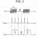
- FIG. 3 illustrates a radio signal V RF , a pulse V PULSE , and a received signal V OUT .
- the radio signal V RF is a signal modulated by OOK, and may correspond to "1" or "0".
- An OOK modulation period of the radio signal V RF is 1/fs.
- the pulse V PULSE is generated at a period less than or equal to 1/2 times 1/f s , which is the OOK modulation period of the radio signal V RF .
- f s is a data frequency or a data rate.
- the received signal V OUT corresponds to a value to which the radio signal V RF corresponds during an interval in which the pulse V PULSE is provided.
- the radio signal V RF corresponds to "1" at first, second, fifth, and sixth points in time at which a pulse is provided, and thus the received signal V OUT corresponds to "1" at the first, second, fifth, and sixth points in time.
- the radio signal V RF corresponds to "0" at third and fourth points in time in which a pulse is provided, and thus the received signal V OUT corresponds to "0" at the third and fourth points in time.
- a receiver operates based on the pulse V PULSE and measures an oscillation time of an oscillation signal using a TDC whereby the radio signal V RF is accurately received during a relatively short pulse period.
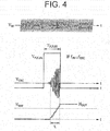
- the radio signal V RF corresponds to "1".
- the pulse V PULSE is high during T PULSE .
- the oscillation signal V OSC starts oscillating quickly in an oscillator. For example, the oscillation signal V OSC starts oscillating starting from a point in time relatively close to a rising edge of the pulse V PULSE .
- the oscillation signal V OSC starts oscillating quickly, an interval in which an amplitude of the oscillation signal V OSC is greater than or equal to a predetermined amplitude increases.
- a TDC measures a length of the interval in which the amplitude of the oscillation signal V OSC is greater than the predetermined amplitude. For example, an output count N OUT of the TDC is proportional to an oscillation time t 1 of the oscillation signal V OSC .
- a receiver receives the radio signal V RF corresponding to "1".
- the threshold time corresponds to a threshold count N REF .
- the output count N OUT of the TDC is greater than a threshold count N REF , it is determined that the oscillation time t 1 of the oscillation signal V OSC is greater than the threshold time.
- the radio signal V RF corresponds to "0".
- the oscillation signal Vosc starts oscillating slowly in the oscillator.
- the oscillation signal V OSC starts oscillating starting from a point in time relatively far from the rising edge of the pulse V PULSE .
- the interval in which the amplitude of the oscillation signal V OSC is greater than or equal to the predetermined amplitude decreases.
- the TDC continuously increases the output count N OUT starting from zero during the interval in which the amplitude of the oscillation signal V OSC is greater than the predetermined amplitude.
- the longer the interval in which the amplitude of the oscillation signal V OSC is greater than the predetermined amplitude the higher the output count N OUT .
- an oscillation time to of the oscillation signal V OSC is obtained based on the output count N OUT of the TDC.
- the receiver receives the radio signal V RF corresponding to "0".
- the threshold time corresponds to the threshold count N REF .
- the oscillation time to of the oscillation signal Vosc is less than the threshold time.
- the oscillation time to of the oscillation signal V OSC of FIG. 5 is less than the oscillation time t 1 of the oscillation signal V OSC in FIG. 4 .
- FIG. 6 illustrates an example of a procedure of receiving a radio signal using a TDC.
- the radio signal V RF is a signal modulated by OOK and corresponds to "1", “0", “1", and "0".
- An OOK modulation period of the radio signal V RF is T S , which corresponds to 1/f s shown in FIG. 3 .
- the pulse V PULSE is generated in a pulse generator at an interval of a predetermined period.
- the pulse V PULSE is generated at an interval of a predetermined period less than or equal to 1/2 times the OOK modulation period T S of the radio signal V RF .
- a receiver is powered on during an interval in which the pulse V PULSE is generated. Also, the receiver is powered off during an interval in which the pulse V PULSE is not generated.
- the interval in which the pulse V PULSE is generated has a length of T PULSE .
- an oscillator driven by the pulse V PULSE generates the oscillation signal V OSC based on the radio signal V RF .
- an oscillation time of the oscillation signal V OSC that is generated during an interval in which the radio signal V RF corresponds to "1" is greater than an oscillation time of the oscillation signal V OSC that is generated during an interval in which the radio signal V RF corresponds to "0".
- a TDC driven by the pulse V PULSE generates the output count N OUT proportionally to an oscillation time of the oscillation signal Vosc. For example, an oscillation time of the oscillation signal V OSC generated during the interval in which the radio signal V RF is "1" is greater than a threshold time. In this example, the output count N OUT of the TDC is greater than the threshold count N REF , and thus the receiver receives the radio signal V RF corresponding to "1". Also, an oscillation time of the oscillation signal V OSC generated during the interval in which the radio signal V RF is "0" is less than the threshold time. Thus, the output count N OUT of the TDC is less than the threshold count N REF , and thus the receiver receives the radio signal V RF corresponding to "0".
- the TDC continues to output the output count N OUT until a reset signal (not illustrated in FIG. 6 ) is input to the TDC to reset the output count N OUT to 0.
- the reset signal is input to the TDC before a pulse subsequent to the pulse V PULSE is generated to reset the output count N OUT to 0.
- the threshold count N REF may be predetermined or may be dynamically changed based on output counts N OUT of the TDC produced by a predetermined radio signal.
- a predetermined radio signal "1, 0, 1, 0" is input to the oscillator and causes the TDC to produce output counts N OUT "10, 5, 10, 5"
- the threshold count N REF is dynamically set to 7.5. That is, the threshold count N REF is dynamically set to a value halfway between the output count N OUT 10 produced by the radio signal "1" and the output count N OUT 5 produced by the radio signal "0.”.
- the predetermined radio signal "1, 0, 1, 0" may produce other output counts N OUT , or other predetermined radio signals may be used, or the threshold count N REF may be dynamically set using other schemes.
- FIG. 7 illustrates another example of a receiver including a TDC.
- a receiver 700 includes a controller 710, a receiving main block, for example, an RX main block 720, and an antenna 730.
- the receiver 700 is, for example, an RF transceiver.
- the controller 710 generates a pulse V PULSE and provides the pulse V PULSE to the RX main block 720.
- a resistor-capacitor (RC)-oscillator is a clock generator configured to generate a clock signal and provides a generated clock signal V RC to a pulse generator.
- the pulse generator generates a pulse V PULSE based on the clock signal V RC and provides the pulse V PULSE to an oscillator, an RF amplifier, for example, an operational amplifier, and a TDC in the RX main block 720.
- the pulse V PULSE is generated at an interval of a period determined by a frequency divider, and a width of the pulse V PULSE is determined by the pulse generator.
- a fast startup circuit is a circuit that enables an oscillation signal V OSC to be rapidly generated in an oscillator in order to reduce the width of the pulse V PULSE , will be described with reference to FIGS. 12 through 14 .
- the antenna 730 and a plurality of capacitors of a CAP bank form a tank circuit of the oscillator.
- the antenna 730 serves as an inductor of the tank circuit.
- the oscillator in the RX main block 720 is driven by the pulse V PULSE to generate the oscillation signal Vosc based on a radio signal received by the antenna 730.
- the oscillation signal Vosc is amplified by the RF amplifier.
- the RF amplifier is driven by the pulse V PULSE .
- FIG. 7 illustrates two RF amplifiers as one example, the RX main block 720 may include one RF amplifier or three or more RF amplifiers without restriction.
- the TDC outputs an output count N OUT that is proportional to an oscillation time of an amplified oscillation signal V OSC2 driven by the pulse V PULSE .
- the TDC receives a reset signal V RST from a reset controller, for example, an RST controller, and resets the output count N OUT before a pulse subsequent to the pulse V PULSE is provided.
- a synchronizer performs phase synchronization on a clock signal V SAM and the output count N OUT of the TDC. Also, a synchronized signal Vs is compared to a threshold voltage V REF in a comparator so that a received signal V OUT is output.
- the threshold voltage V REF corresponds to the aforementioned threshold count N REF .
- FIG. 8 illustrates an example of a procedure of receiving a radio signal in the receiver of FIG. 7 .
- FIG. 8 illustrates a radio signal V RF , a pulse V PULSE , an oscillation signal Vosc, amplified oscillation signals V OSC1 and V OSC2 , and an output count N OUT of a TDC.
- the radio signal V RF is "1" when the pulse V PULSE is generated.
- the receiver operates and receives and outputs the radio signal V RF .
- the receiver does not operate and continues to output a previously received signal.
- the pulse V PULSE is provided during a time T PULSE .
- the time T PULSE is greater than a startup time T SET .
- the startup time T SET will be described with reference to FIG. 9 .
- the oscillation signal Vosc is generated based on the radio signal V RF in an oscillator driven by the pulse V PULSE .
- the oscillation signal V OSC is amplified using at least one RF amplifier.
- V OSC1 and V OSC2 represent amplified oscillation signals.
- the TDC outputs an output count N OUT proportional to an oscillation time t 1 based on the amplified oscillation signal V OSC2 .
- the TDC outputs the output count N OUT proportional to the oscillation time t 1 by continuing to increment the output count N OUT as long as an amplitude of the amplified oscillation signal V OSC2 is greater than a threshold amplitude.
- the TDC continues to output the output count N OUT until a reset signal is input to the TDC.
- FIG. 9 illustrates an example of a procedure of generating an output of a TDC based on a radio signal.
- FIG. 9 illustrates a startup time T SET and an operation time T SS of a TDC.
- a receiver is powered on during an interval in which the pulse V PULSE is generated.
- the receiver operates based on impulse-based carrier sensing (IBCS) so that the receiver is powered on during an interval in which the pulse V PULSE is generated, and powered off during an interval in which the pulse V PULSE is not generated.
- IBCS impulse-based carrier sensing
- a width T PULSE of the pulse V PULSE is divided into the startup time T SET and the operation time Tss of the TDC.
- the startup time T SET is an interval in which an output is not generated in the TDC because an amplitude of an oscillation signal is less than or equal to a threshold amplitude.
- the operation time Tss is be an interval in which an output is generated in the TDC because the amplitude of the oscillation signal is greater than the threshold amplitude.
- the width T PULSE of the pulse V PULSE is expressed by Equation 1 below.
- T OSC denotes an oscillation period of an oscillator and f OSC denotes an oscillation frequency of the oscillator, where f OSC is a high frequency and may also be referred to as a carrier frequency.
- Equation 1 when the startup time T SET is reduced, or when the oscillation frequency f OSC increases, the width T PULSE of the pulse V PULSE is effectively reduced, and thus power consumption in the receiver is also reduced.
- T 1 represents a time measured in the TDC when the radio signal V RF is "1" and To represents a time measured in the TDC when the radio signal V RF is "0".
- the radio signal V RF is modulated by OOK.
- an output count N OUT of the TDC is proportional to the amplitude of the radio signal V RF so that the radio signal V RF is received without restrictions.
- the output count N OUT of the TDC is inversely proportional to a frequency difference between a frequency of the radio signal V RF and the oscillation frequency of the oscillation signal, whereby the radio signal V RF is received without restrictions.
- FIG. 10 illustrates an example of an output of a TDC that is not affected by jitter of a clock generator.
- FIG. 10 illustrates a radio signal V RF , a clock signal V RC generated in a clock generator, and a pulse V PULSE generated in a pulse generator.
- the clock signal V RC includes jitter.
- Jitter is a phenomenon in which a period of the clock generator generating the clock signal V RC deviates from its normal value.
- An oscillator generates the pulse V PULSE at a rising edge of the clock signal V RC .
- the jitter causes a pulse position fluctuation denoted by ⁇ T RC to appear at the rising edge of the clock signal V RC .
- a position fluctuation occurs in an output count N OUT of a TDC due to the pulse position fluctuation. Also, a point in time at which an output of the TDC is reset is changed based on a reset signal V RST .
- a receiver receives the radio signal V RF based on the output count N OUT of the TDC, and thus is not affected by the jitter of the clock generator.
- the output count N OUT of the TDC is proportional to a width of the pulse V PULSE and an oscillation frequency of an oscillation signal, and is not affected by the jitter of the clock generator.
- the receiver receives the radio signal V RF robustly despite the jitter of the clock generator therein.
- FIG. 11 illustrates an example of a TDC output change based on a change in a width of a pulse.
- FIG. 11 illustrates a pulse V PULSE , an output count N OUT of a TDC, and a reset signal V RST .
- a minimum width of the pulse V PULSE is a width that enables the TDC to output an effective output count N OUT_effective that is capable of receiving a radio signal.
- a minimum pulse width W min and a minimum duty cycle D min of the pulse V PULSE are determined using Equation 2 below.
- the minimum duty cycle D min is a ratio of an interval in which the pulse V PULSE is high to an interval at which the pulse V PULSE is generated.
- D min N OUT_effective + f OSC ⁇ T SET ⁇ f RC f OSC
- Equation 2 f RC denotes a frequency of a clock generator. It can be seen from Equation 2 that the minimum pulse width W min is proportional to a startup time T SET of an oscillator.
- Equation 3 P RX denotes a power consumption of the receiver, and T RC denotes a period of the clock generator. It can be seen from Equation 3 that the average power consumption P AVE of the receiver is proportional to the startup time T SET of the oscillator. Thus, the startup time T SET is to be minimized to minimize the power consumption of the receiver. A fast startup method that minimizes the startup time T SET will be described with reference to FIGS. 12 and 13 .
- FIG. 12 illustrates an example of a fast startup of a receiver.
- FIG. 12 illustrates an additional current I QWG_A for a fast startup and a control voltage V PUL_C for controlling whether capacitors of a tank circuit of an oscillator have equal or unequal values.
- a startup time T SET is an oscillation startup interval for generating an oscillation signal Vosc.
- the TDC does not generate an output in the oscillation startup interval.
- a receiver is powered on to receive the radio signal V RF , which consumes power.
- the power consumption of the receiver is minimized by minimizing the startup time T SET .
- the startup time T SET is minimized by the fast startup as follows.
- the fast startup is achieved by controlling a current I QWG provided to an oscillator.
- a base current I QWG _ O provided to the oscillator is constant during a period of time from a start point in time t a corresponding to a rising edge of a pulse V PULSE to an end point in time t c corresponding to a falling edge of the pulse V PULSE .
- the additional current I QWG_A for the fast startup is provided to the oscillator.
- the additional current I QWG_A is provided to the oscillator during a period of time from the start point in time t a to an intermediate point in time t b .
- the current I QWG provided to the oscillator is greater in a first period of time from the start point in time t a to the intermediate point in time t b than in a second period of time from the intermediate point in time t b to the end point in time t c .
- the startup time T SET is minimized by controlling the current I QWG .
- FIG. 13 illustrates an example of a receiver having a fast startup function.
- a receiver includes an antenna 1310, a pulse generator, a phase splitter, a current supplier QWG that outputs the base current I QWG_O , a current supplier A-QWG that outputs the additional current I QWG_A , an adder that adds the base current I QWG_O and additional current I QWG_A to obtain the current I QWG , the oscillator, and capacitors C 1 and C 2 .
- the fast startup is achieved by controlling a plurality of capacitors applied to the oscillator.
- the oscillator is an LC-oscillator including a tank circuit formed by the antenna 1310 and the capacitors C 1 and C 2
- the antenna 1310 serves as an inductor of the tank circuit.
- the control voltage V PUL_C is controlled so that the value k is a value other than 1, for example, a value between 1.8 and 2.0, during the first period of time from the start point in time t a to the intermediate point in time t b .
- the control voltage V PUL_C is controlled so that the value k is 1 during the second period of time from the intermediate point in time t b to the end point in time t c .
- the capacitors C 1 and C 2 are controlled to have unequal values, i.e., to be asymmetric to each other, during the first period of time from the start point in time t a to the intermediate point in time t b , and controlled to have equal values, i.e., to be symmetric to each other, during the second period of time from the intermediate point in time t b to the end point in time t b , thereby minimizing the startup time T SET .
- the fast startup is achieved by using an inductor having a Q-value greater than a threshold in the tank circuit of the oscillator.
- the oscillator is an LC-oscillator in which the antenna 1310 serves as the inductor.
- the startup time T SET is expressed by Equation 5 below.
- Equation 5 g m denotes a transconductance of a core transistor of the oscillator, w 0 denotes an oscillation frequency of the oscillator, and R T denotes an output resistance of the oscillator.
- the core transistor of the oscillator is not shown in FIG. 13 .
- R T is proportional to a square of the Q-value.
- FIG. 12 illustrates that the intermediate point in time t b is a boundary point between the startup time T SET and the operation time T SS of the TDC
- the intermediate point in time t b may also be a point between the start point in time t a and the end point in time t c , for example, a point in time that divides the period of time from the start point in time t a to the end point in time t c in half.
- FIG. 14 illustrates an example of a receiver including a pulse width controller.
- a receiver 1400 includes a controller 1410, a receiving main block 1420, and an antenna 1430.
- the receiver 1400 is, for example, an RF transceiver.
- the controller 1410 generates a pulse V PULSE and provides the pulse V PULSE to the receiving main block 1420.
- the controller 1410 includes a low-power RC-oscillator and a main RC-oscillator having different oscillation frequencies as clock generators.
- the low-power RC-oscillator is a clock generator configured to generate a clock signal having a lower frequency than a clock signal generated by the main RC-oscillator.
- the pulse V PULSE is generated in a pulse generator at an interval of a relatively long period. In this example, a power consumption of the receiver 1400 is less when compared to a case in which the main RC-oscillator is used.
- a clock signal V RC1 is a clock signal generated in the low-power RC-oscillator
- a clock signal V RC2 is a clock signal generated in the main RC-oscillator.
- the controller 1410 selects one of the low-power RC-oscillator and the main RC-oscillator based on a frequency of a radio signal received by the antenna 1430.
- An oscillator capable of generating a clock signal at a frequency that is at least twice the frequency of the radio signal is selected from the low-power RC-oscillator and the main RC-oscillator.
- the low-power RC-oscillator is selected so that the power consumption of the receiver 1400 is reduced.
- a current supplier provides a current I QWG to an oscillator and corresponds to QWG and A-QWG of FIG. 13 .
- a fast startup circuit generates a control voltage V PUL_C for controlling whether capacitors of a tank circuit of an oscillator have equal or unequal values, and corresponds to a phase splitter of FIG. 13 .
- a CAP bank includes a plurality of capacitors and corresponds to the capacitors C 1 and C 2 of FIG. 13 .
- the antenna 1430 and the plurality of capacitors of the CAP bank form a tank circuit of the oscillator.
- the antenna 1430 serves as an inductor of the tank circuit.
- a pulse width controller controls a width of the pulse V PULSE generated in the oscillator.
- the pulse width controller controls the width of the pulse V PULSE based on an output N OUT of a TDC.
- the width of the pulse V PULSE increases, an operation time of the receiver 1400 increases and the power consumption of the receiver 1400 also increases.
- the width of the pulse V PULSE is minimized to minimize the power consumption of the receiver 1400.
- the pulse width controller minimizes the width of the pulse V PULSE within a range in which the effective output is generated in the TDC.
- the width of the pulse V PULSE may be adjusted based on a radio signal, for example, "1, 0, 1, 0", received by the antenna 1430. For example, based on the output counts N OUT of the TDC produced by the radio signal "1, 0, 1, 0", the pulse width controller adjusts the width of the pulse V PULSE to a minimum width that still enables the radio signal to be effectively received.
- FIGS. 1 through 13 The description of FIGS. 1 through 13 is also applicable to FIG. 14 , but will not be repeated here for brevity.
- FIG. 15 illustrates an example of a power consumption of a receiver.
- FIG. 15 illustrates cases in which a pulse width and a data rate affect a power consumption of a receiver.
- a data rate affects a power consumption of a receiver.
- radio signals having different data rates are received.
- a pulse period is to be less than or equal to 1/2 times an OOK modulation period of a radio signal. Because of this, the receiver is powered on to operate more frequently in the case 1510 having a higher data rate than in the case 1520 having a lower data rate. Thus, the receiver uses a smaller amount of power in the case 1520 than in the case 1510. As the data rate of the radio signal decreases, the power consumption of the receiver decreases.
- the pulse width affects the power consumption of the receiver.
- a case 1530 and a case 1540 represent examples associated with different pulse widths. Since the receiver is powered on and operates in an interval in which a pulse is high, the power consumption of the receiver increases proportionally to the pulse width. Thus, the receiver uses a smaller amount of power in the case 1540 in which the pulse width is smaller than in the case 1530 in which the pulse width is larger. As the pulse width decreases, the power consumption of the receiver decreases.
- FIG. 16 illustrates an example of a receiver including an envelope detector (ED).
- ED envelope detector
- a receiver 1600 includes an antenna 1610, a clock generator 1620, a pulse generator 1630, an oscillator 1640, an ED 1650, an RF amplifier 1660, and an analog-to-digital converter (ADC) 1670.
- the measurer 140 of FIG. 1 corresponds to, for example, the ED 1650.
- the receiver 1600 receives a radio signal V RF based on an envelope V ED of an oscillation signal V OSC detected using the ED 1650.
- the radio signal V RF is received by the antenna 1610.
- the clock generator 1620 generates a clock signal and provides the clock signal to the pulse generator 1630.
- the pulse generator 1630 generates a pulse V PULSE at an interval of a predetermined period based on the received clock signal.
- the oscillator 1640 may be an LC-oscillator driven by the pulse V PULSE to generate the oscillation signal Vosc based on the radio signal V RF .
- FIGS. 1 through 15 Since the description of FIGS. 1 through 15 is also applicable to the antenna 1610, the clock generator 1620, the pulse generator 1630, and the oscillator 1640, repeated description will be omitted.
- the ED 1650 detects the envelope V ED of the oscillation signal V OSC .
- the detected envelope V ED is amplified by the RF amplifier 1660.
- V ED1 represents an amplified envelope.
- FIG. 16 illustrates one RF amplifier as one example, the receiver 1600 may include two or more RF amplifiers without restriction.
- the ADC 1670 converts the envelope V ED in an analog form into a digital signal.
- the digital signal obtained in the ADC 1670 is compared to a threshold, and the radio signal V RF is received based on a result of the comparison.
- the radio signal V RF is received as "1".
- the radio signal V RF is received as "0".
- a received signal is output as a received signal V OUT .
- FIG. 17 illustrates an example of a procedure of receiving a radio signal in the receiver of FIG. 16 .
- FIG. 17 illustrates a radio signal V RF , a pulse V PULSE , an envelope signal V ED , an amplified envelope signal V ED1 , and a received signal V OUT ,
- the pulse V PULSE is generated at a frequency that is at least twice a frequency of the radio signal V RF .
- an oscillation signal is generated in an oscillator and the envelope signal V ED of the oscillation signal is detected.
- the envelope signal V ED is amplified by an RF amplifier.
- An amplitude of the amplified envelope signal V ED1 is compared to a threshold amplitude.
- the received signal V OUT is output based on a result of the comparison.
- FIG. 18 illustrates an example of a reception method.
- the reception method is performed by a receiver.
- the receiver In operation 1810, the receiver generates a pulse with a predetermined width at an interval of a predetermined period.
- the predetermined period is, for example, a period less than 1/2 times an OOK modulation period of a radio signal received by an antenna.
- the receiver In operation 1820, the receiver generates, during the pulse, an oscillation signal based on the radio signal received by the antenna.
- the generating is enabled based on the pulse.
- the receiver When the input radio signal is "1", the receiver more quickly initiates an oscillation and performs the oscillation during a longer period of time than in a case in which the input radio signal is "0".
- the receiver measures, during the pulse, an oscillation degree of the oscillation signal.
- the measuring is enabled based on the pulse.
- the receiver includes a TDC
- the receiver generates an output of the TDC proportional to an oscillation time of the oscillation signal as the oscillation degree of the oscillation signal.
- the receiver includes an ED
- the receiver detects an envelope of the oscillation signal as the oscillation degree of the oscillation signal.
- a radio signal is received based on the measured oscillation degree. For example, the radio signal is received based on whether the generated output of the TDC is greater than a threshold. Alternatively, the radio signal is received based on whether an amplitude of the detected envelope is greater than a threshold.
- a receiver is provided with a low power consumption and a high receive sensitivity and without latency. Also, the receiver minimizes an active interval based on a short pulse and generally operates in a turn-off state, thereby minimizing the power consumption. Also, the receiver is powered on at an interval of a period less than or equal to 1/2 times an OOK modulation period of a radio signal. This causes the receiver to operate in a minimum active interval without latency, thereby minimizing an average power consumption.
- FIGS. 1 through 17 The description of FIGS. 1 through 17 is also applicable to FIG. 18 , but will not be repeated here for brevity.
- FIG. 19 illustrates an example of a method of controlling a width of a pulse generated in a pulse generator.
- a procedure of controlling a width of a pulse is performed by a receiver.
- the receiver determines whether a measured oscillation degree is greater than a threshold.
- the receiver determines whether an output generated in the TDC is greater than the threshold.
- the receiver includes an ED, the receiver determines whether an amplitude of a detected envelope is greater than the threshold.
- the receiver When the measured oscillation degree is greater than the threshold, the receiver reduces a width of a pulse output from a pulse generator in operation 1920. For example, the receiver reduces the width of the pulse by a predetermined amount or ratio.
- the receiver increases the width of the pulse output from the pulse generator in operation 1930. For example, the receiver increases the width of the pulse by a predetermined amount or ratio.
- FIGS. 1 through 18 The description of FIGS. 1 through 18 is also applicable to FIG. 19 , but will not be repeated here for brevity.
- TDC time-to-digital converter
- ADC analog-to-digital-converter
- Examples of hardware components that may be used to perform the operations described in this application where appropriate include controllers, sensors, generators, drivers, memories, comparators, arithmetic logic units, adders, subtractors, multipliers, dividers, integrators, and any other electronic components configured to perform the operations described in this application.
- one or more of the hardware components that perform the operations described in this application are implemented by computing hardware, for example, by one or more processors or computers.
- a processor or computer may be implemented by one or more processing elements, such as an array of logic gates, a controller and an arithmetic logic unit, a digital signal processor, a microcomputer, a programmable logic controller, a field-programmable gate array, a programmable logic array, a microprocessor, or any other device or combination of devices that is configured to respond to and execute instructions in a defined manner to achieve a desired result.
- a processor or computer includes, or is connected to, one or more memories storing instructions or software that are executed by the processor or computer.
- Hardware components implemented by a processor or computer may execute instructions or software, such as an operating system (OS) and one or more software applications that run on the OS, to perform the operations described in this application.
- OS operating system
- the hardware components may also access, manipulate, process, create, and store data in response to execution of the instructions or software.
- processor or “computer” may be used in the description of the examples described in this application, but in other examples multiple processors or computers may be used, or a processor or computer may include multiple processing elements, or multiple types of processing elements, or both.
- a single hardware component or two or more hardware components may be implemented by a single processor, or two or more processors, or a processor and a controller.
- One or more hardware components may be implemented by one or more processors, or a processor and a controller, and one or more other hardware components may be implemented by one or more other processors, or another processor and another controller.
- One or more processors may implement a single hardware component, or two or more hardware components.
- a hardware component may have any one or more of different processing configurations, examples of which include a single processor, independent processors, parallel processors, single-instruction single-data (SISD) multiprocessing, single-instruction multiple-data (SIMD) multiprocessing, multiple-instruction single-data (MISD) multiprocessing, and multiple-instruction multiple-data (MIMD) multiprocessing.
- SISD single-instruction single-data
- SIMD single-instruction multiple-data
- MIMD multiple-instruction multiple-data
- FIGS. 3-6 , 8-12 , 15 , and 17-19 that perform the operations described in this application are performed by computing hardware, for example, by one or more processors or computers, implemented as described above executing instructions or software to perform the operations described in this application that are performed by the methods.
- a single operation or two or more operations may be performed by a single processor, or two or more processors, or a processor and a controller.
- One or more operations may be performed by one or more processors, or a processor and a controller, and one or more other operations may be performed by one or more other processors, or another processor and another controller.
- One or more processors, or a processor and a controller may perform a single operation, or two or more operations.
- Instructions or software to control computing hardware may be written as computer programs, code segments, instructions or any combination thereof, for individually or collectively instructing or configuring the one or more processors or computers to operate as a machine or special-purpose computer to perform the operations that are performed by the hardware components and the methods as described above.
- the instructions or software include machine code that is directly executed by the one or more processors or computers, such as machine code produced by a compiler.
- the instructions or software includes higher-level code that is executed by the one or more processors or computer using an interpreter.
- the instructions or software may be written using any programming language based on the block diagrams and the flow charts illustrated in the drawings and the corresponding descriptions in the specification, which disclose algorithms for performing the operations that are performed by the hardware components and the methods as described above.
- the instructions or software to control computing hardware for example, one or more processors or computers, to implement the hardware components and perform the methods as described above, and any associated data, data files, and data structures, may be recorded, stored, or fixed in or on one or more non-transitory computer-readable storage media.
- Examples of a non-transitory computer-readable storage medium include read-only memory (ROM), random-access memory (RAM), flash memory, CD-ROMs, CD-Rs, CD+Rs, CD-RWs, CD+RWs, DVD-ROMs, DVD-Rs, DVD+Rs, DVD-RWs, DVD+RWs, DVD-RAMs, BD-ROMs, BD-Rs, BD-R LTHs, BD-REs, magnetic tapes, floppy disks, magneto-optical data storage devices, optical data storage devices, hard disks, solid-state disks, and any other device that is configured to store the instructions or software and any associated data, data files, and data structures in a non-transitory manner and provide the instructions or software and any associated data, data files, and data structures to one or more processors or computers so that the one or more processors or computers can execute the instructions.
- ROM read-only memory
- RAM random-access memory
- flash memory CD-ROMs, CD-Rs, CD
- the instructions or software and any associated data, data files, and data structures are distributed over network-coupled computer systems so that the instructions and software and any associated data, data files, and data structures are stored, accessed, and executed in a distributed fashion by the one or more processors or computers.
Abstract
Description
- The following description relates to a receiver and a reception method based on a pulse.
- Recently, with development of information and communication technology, internet of things (loT) devices that transmit and receive data in real time by attaching sensors to objects are becoming popular. The loT device may be a subminiature wireless transceiver configured to perform communication at a low power to process information by performing transmission and reception of the information between distributed elements such as objects. To provide the loT devices in subminiature sizes and implement a low power communication system, wireless communication needs to be performed with a low power, a high receive sensitivity, and no latency.
- This Summary is provided to introduce a selection of concepts in a simplified form that are further described below in the Detailed Description. This Summary is not intended to identify key features or essential features of the claimed subject matter, nor is it intended to be used as an aid in determining the scope of the claimed subject matter.
- In one general aspect, a receiver includes an antenna configured to receive a radio signal; a pulse generator configured to generate a pulse; an oscillator configured to be driven based on the pulse to generate an oscillation signal based on the radio signal; and a measurer configured to be driven based on the pulse to measure an oscillation degree of the oscillation signal, wherein the radio signal is received based on the oscillation degree of the oscillation signal.
- The measurer may be further configured to measure an oscillation time of the oscillation signal as the oscillation degree of the oscillation signal, and the radio signal may be received based on the oscillation time of the oscillation signal.
- The measurer may be further configured to generate an output proportional to the oscillation time of the oscillation signal, and the radio signal may be received based on whether the generated output is greater than a threshold.
- The radio signal may be received as a first value in response to the oscillation time being greater than or equal to a threshold time, and received as a second value different from the first value in response to the oscillation time being less than the threshold time.
- An amplitude or a frequency of the radio signal received by the antenna may be received based on the oscillation time of the oscillation signal.
- An current supplier may be further configured to provide a first current to the oscillator in a first period of time from a start point in time of the pulse to an intermediate point in time between the start point in time of the pulse and an end point in time of the pulse, and provide a second current smaller than the first current to the oscillator in a second period of time from the intermediate point in time to the end point in time of the pulse.
- The oscillator may include a tank circuit including a plurality of capacitors, and the plurality of capacitors may have unequal values in a first period of time from a start point in time of the pulse to an intermediate point in time between the start point in time of the pulse and an end point in time of the pulse, and equal values in a second period of time from the intermediate point in time to the end point in time of the pulse.
- The receiver may further include an inductor having a Q-value greater than a threshold applied to the oscillator.
- The measurer may be further configured to generate an output proportional to an oscillation time of the oscillator, and the pulse generator may be further configured to adjust a width of the pulse based on the output generated by the measurer.
- The measurer may be further configured to generate an output proportional to an oscillation frequency of the oscillation signal and a width of the pulse based on an oscillation time of the oscillation signal.
- The pulse generator may be further configured to generate the pulse at an interval of a period less than 1/2 times an on-off keying (OOK) modulation period of the radio signal.
- The measurer may be further configured to detect an envelope of the oscillation signal as the oscillation degree of the oscillation signal, and the radio signal may be received based on the envelope of the oscillation signal,
- The measurer may be further configured to measure an amplitude of the detected envelope of the oscillation signal, and the radio signal is received based on whether the amplitude of the detected envelope is greater than a threshold.
- The oscillator and the measurer may be further configured to operate during an interval in which the oscillator and the measurer receive the pulse from the pulse generator.
- A power consumption of the receiver may be determined by a data rate of the radio signal and a width of the pulse.
- The receiver may further include a radio frequency (RF) amplifier configured to be driven based on the pulse to amplify the oscillation signal and output the amplified oscillation signal to the measurer.
- In another general aspect, a reception method includes generating a pulse at an interval of a predetermined period; generating, during the pulse, an oscillation signal based on a radio signal received by an antenna, the generating being enabled based on the pulse; and measuring, during the pulse, an oscillation degree of the oscillation signal, the measuring being enabled based on the pulse, wherein the radio signal is received based on the oscillation degree of the oscillation signal.
- The measuring may include generating an output proportional to an oscillation time of the oscillation signal as the oscillation degree of the oscillation signal, and the radio signal may be received based on whether the generated output is greater than a threshold.
- The measuring may include detecting an envelope of the oscillation signal as the oscillation degree of the oscillation signal, and the radio signal may be received based on whether an amplitude of the detected envelope is greater than a threshold.
- In another general aspect, a non-transitory computer-readable medium stores instructions that, when executed by a processor, control the processor to perform the reception method described above.
- In another general aspect, a receiver includes an antenna configured to receive a radio signal; a pulse generator configured to generate a pulse at an interval of a predetermined period; an oscillator configured to be powered on by the pulse to generate an oscillation signal based on the radio signal only while the pulse is present; and a measurer configured to be powered on by the pulse to measure a parameter of the oscillation signal depending on the radio signal only while the pulse is present, wherein the radio signal is received based on the parameter of the oscillation signal.
- The measurer may be further configured to measure an oscillation time as the parameter of the oscillation signal or detect an envelope of the oscillation signal as the parameter of the oscillation signal, and the radio signal may be received based on the oscillation time of the oscillation signal or the envelope of the oscillation signal.
- The receiver may further include a fast startup circuit configured to reduce a startup time of the oscillator during a first portion of the pulse by either one or both of increasing a current supplied to the oscillator during the first portion of the pulse, and adjusting a value of a capacitor applied to the oscillator during the first portion of the pulse.
- The oscillator may be a first oscillator configured to generate a first clock signal having a first frequency and requiring a first power level to operate, the receiver may further include a second oscillator configured to generate a second clock signal having a second frequency lower than the first frequency and requiring a second power level lower than the first power level to operate, and a selector configured to select one of the first clock signal and the second clock signal based on the radio signal, and the pulse generator may be further configured to generate the pulse at the interval of the predetermined period based on the selected one of the first clock signal and the second clock signal.
- The selector may be further configured to select the first clock signal in response to the first frequency being at least twice a frequency of the radio signal and the second frequency being less than twice the frequency of the radio signal, and select the second clock signal in response to both the first frequency and the second frequency being at least twice the frequency of the radio signal.
- Other features and aspects will be apparent from the following detailed description, the drawings, and the claims.
-
-
FIG. 1 illustrates an example of a receiver. -
FIG. 2 illustrates an example of a receiver including a time-to-digital converter (TDC). -
FIGS. 3 through 6 illustrate an example of a procedure of receiving a radio signal in the receiver ofFIG. 2 . -
FIG. 7 illustrates another example of a receiver including a TDC. -
FIG. 8 illustrates an example of a procedure of receiving a radio signal in the receiver ofFIG. 7 . -
FIG. 9 illustrates an example of a procedure of generating an output of a TDC based on a radio signal. -
FIG. 10 illustrates an example of an output of a TDC that is not affected by jitter of a clock generator. -
FIG. 11 illustrates an example of a TDC output change based on a change in a width of a pulse. -
FIG. 12 illustrates an example of a fast startup of a receiver. -
FIG. 13 illustrates an example of a receiver having a fast startup function. -
FIG. 14 illustrates an example of a receiver including a pulse width controller. -
FIG. 15 illustrates an example of a power consumption of a receiver. -
FIG. 16 illustrates an example of a receiver including an envelope detector (ED). -
FIG. 17 illustrates an example of a procedure of receiving a radio signal in the receiver ofFIG. 16 . -
FIG. 18 illustrates an example of a reception method. -
FIG. 19 illustrates an example of a method of controlling a width of a pulse generated in a pulse generator. - Throughout the drawings and the detailed description, the same reference numerals refer to the same elements. The drawings may not be to scale, and the relative size, proportions, and depiction of elements in the drawings may be exaggerated for clarity, illustration, and convenience.
- The following detailed description is provided to assist the reader in gaining a comprehensive understanding of the methods, apparatuses, and/or systems described herein. However, various changes, modifications, and equivalents of the methods, apparatuses, and/or systems described herein will be apparent after an understanding of the disclosure of this application. For example, the sequences of operations described herein are merely examples, and are not limited to those set forth herein, but may be changed as will be apparent after an understanding of the disclosure of this application, with the exception of operations necessarily occurring in a certain order. Also, descriptions of features that are known in the art may be omitted for increased clarity and conciseness.
- The features described herein may be embodied in different forms, and are not to be construed as being limited to the examples described herein. Rather, the examples described herein have been provided merely to illustrate some of the many possible ways of implementing the methods, apparatuses, and/or systems described herein that will be apparent after an understanding of the disclosure of this application.
- Although terms such as "first," "second," and "third" may be used herein to describe various members, components, regions, layers, or sections, these members, components, regions, layers, or sections are not to be limited by these terms. Rather, these terms are only used to distinguish one member, component, region, layer, or section from another member, component, region, layer, or section. Thus, a first member, component, region, layer, or section referred to in examples described herein may also be referred to as a second member, component, region, layer, or section without departing from the teachings of the examples.
- Throughout the specification, when an element, such as a layer, region, or substrate, is described as being "on," "connected to," or "coupled to" another element, it may be directly "on," "connected to," or "coupled to" the other element, or there may be one or more other elements intervening therebetween. In contrast, when an element is described as being "directly on," "directly connected to," or "directly coupled to" another element, there can be no other elements intervening therebetween.
- The terminology used herein is for describing various examples only, and is not to be used to limit the disclosure. The articles "a," "an," and "the" are intended to include the plural forms as well, unless the context clearly indicates otherwise. The terms "comprises," "includes," and "has" specify the presence of stated features, numbers, operations, members, elements, and/or combinations thereof, but do not preclude the presence or addition of one or more other features, numbers, operations, members, elements, and/or combinations thereof.
- Unless otherwise defined, all terms, including technical and scientific terms, used herein have the same meaning as commonly understood by one of ordinary skill in the art to which this disclosure pertains. Terms, such as those defined in commonly used dictionaries, are to be interpreted as having a meaning that is consistent with their meaning in the context of the relevant art, and are not to be interpreted in an idealized or overly formal sense unless expressly so defined herein.
-
FIG. 1 illustrates an example of a receiver. - Referring to
FIG. 1 , areceiver 100 includes anantenna 110, apulse generator 120, anoscillator 130, and ameasurer 140. - The
receiver 100 is a device for receiving a radio signal. Thereceiver 100 may be implemented as, for example, a subminiature wireless transceiver such as, for example, a low power communication device, an Internet of things (loT) device, an implantable communication device, or a medical implant communications system (MICS). - A radio signal is received by the
antenna 110. The radio signal is a signal transmitted and received through wireless communication, for example, a radio frequency (RF) signal. In one example, the RF signal is a signal modulated by amplitude shift keying (ASK), for example, on-off keying (OOK). In another example, the RF signal is modulated by frequency shift keying (FSK). For brevity, the following description is provided based on an example in which a radio signal is modulated by OOK. - The
pulse generator 120 generates a pulse. Thepulse generator 120 generates the pulse based on a predetermined period. For example, the predetermined period is less than 1/2 times an OOK modulation period of a radio signal. The pulse generated in thepulse generator 120 is provided to theoscillator 130 and themeasurer 140. - The
oscillator 130 may be an LC-VCO (inductor capacitor-voltage controlled oscillator) driven by the pulse. For example, theoscillator 130 does not operate during an interval in which a pulse is not provided to theoscillator 130, and thus an oscillation signal is not generated in theoscillator 130. Conversely, theoscillator 130 operates in an interval in which the pulse is provided to theoscillator 130, and thus an oscillation signal is generated based on a radio signal. As such, theoscillator 130 operates in a relatively short interval in which the pulse is provided from thepulse generator 120, whereby a power consumption of thereceiver 100 is effectively reduced. - When the pulse is provided to the
oscillator 130, theoscillator 130 generates an oscillation signal based on the radio signal received by theantenna 110. For example, a signal generated in theoscillator 130 based on a radio signal "1" received by theantenna 110 in the interval in which the pulse is provided is different from a signal generated in theoscillator 130 based on a radio signal "0" received by theantenna 110 in the interval in which the pulse is provided. Theoscillator 130 determines whether an RF carrier is present and generates the oscillation signal based on a determination result. The oscillation signal will also be described in detail with reference toFIG. 2 . - The
measurer 140 measures an oscillation degree of the oscillation signal. In this example, themeasurer 140 is also driven by the pulse. Themeasurer 140 is driven to measure the oscillation degree of the oscillation signal during the interval in which the pulse is provided from thepulse generator 120. For example, themeasurer 140 measures an oscillation time of the oscillation signal or an envelope of the oscillation signal as the oscillation degree of the oscillation signal. - A radio signal is received based on the oscillation degree of the oscillation signal measured in the
measurer 140. In one example, the radio signal is received based on an oscillation time of the oscillation signal measured in themeasurer 140. In another example, the radio signal is received based on an envelope of the oscillation signal measured in themeasurer 140. - For brevity, the following description will be provided based on an example in which a radio signal is received based on an oscillation time of an oscillation signal. An example in which a radio signal is received based on an envelope of an oscillation signal will be described with reference to
FIG. 16 . -
FIG. 2 illustrates an example of a receiver including a time-to-digital converter (TDC). - Referring to
FIG. 2 , areceiver 200 includes anantenna 210, aclock generator 220, apulse generator 230, anoscillator 240, and aTDC 250. For example, themeasurer 140 ofFIG. 1 may correspond to theTDC 250. In this example, thereceiver 200 receives a radio signal VRF based on an oscillation time of an oscillation signal VOSC measured using theTDC 250. - The radio signal VRF is received by the
antenna 210. For example, the radio signal VRF is a signal modulated by OOK, and may correspond to "1" or "0". - The
clock generator 220 generates a clock signal and provides the clock signal to thepulse generator 230. Thepulse generator 230 generates a pulse VPULSE at an interval of a predetermined period based on the received clock signal. Theoscillator 240 and theTDC 250 are enabled, for example, powered on, by the pulse VPULSE. - The
oscillator 240 is, for example, an inductor-capacitor (LC) oscillator driven by the pulse VPULSE to generate an oscillation signal VOSC based on the radio signal VRF. Theoscillator 240 generates the oscillation signal VOSC oscillating in a period of time varying based on the radio signal VRF. For example, when the radio signal VRF received by theantenna 210 is "1", theoscillator 240 generates the oscillation signal VOSC oscillating in a greater period of time than in a case in which the radio signal VRF received by theantenna 210 is "0". When the radio signal VRF received by theantenna 210 is "0", theoscillator 240 generates the oscillation signal Vosc oscillating in a lesser period of time than in a case in which the radio signal VRF received by theantenna 210 is "1". - The
TDC 250 measures an oscillation time of the oscillation signal Vosc and outputs an output count NOUT corresponding to the measured oscillation time. TheTDC 250 generates the output count NOUT proportionally to the oscillation time of the oscillation signal VOSC. For example, theTDC 250 generates the output count NOUT based on an oscillating start time of the oscillation signal VOSC. When an amplitude of the oscillation signal Vosc is greater than a threshold amplitude, theTDC 250 recognizes that the oscillation signal VOSC oscillates, and thus generates the output count NOUT. - The
receiver 200 receives the radio signal VRF based on the output count NOUT of theTDC 250. When the output count NOUT of theTDC 250 is greater than or equal to a threshold count NREF, thereceiver 200 receives the radio signal VRF corresponding to "1". When the output count NOUT of theTDC 250 is less than the threshold count NREF, thereceiver 200 receives the radio signal VRF corresponding to "0". -
FIGS. 3 through 6 illustrate an example of a procedure of receiving a radio signal in the receiver ofFIG. 2 . -
FIG. 3 illustrates a radio signal VRF, a pulse VPULSE, and a received signal VOUT. - The radio signal VRF is a signal modulated by OOK, and may correspond to "1" or "0". An OOK modulation period of the radio signal VRF is 1/fs. The pulse VPULSE is generated at a period less than or equal to 1/2
times 1/fs, which is the OOK modulation period of the radio signal VRF. fs is a data frequency or a data rate. - The received signal VOUT corresponds to a value to which the radio signal VRF corresponds during an interval in which the pulse VPULSE is provided. In the example of
FIG. 3 , the radio signal VRF corresponds to "1" at first, second, fifth, and sixth points in time at which a pulse is provided, and thus the received signal VOUT corresponds to "1" at the first, second, fifth, and sixth points in time. Also, the radio signal VRF corresponds to "0" at third and fourth points in time in which a pulse is provided, and thus the received signal VOUT corresponds to "0" at the third and fourth points in time. - As such, a receiver operates based on the pulse VPULSE and measures an oscillation time of an oscillation signal using a TDC whereby the radio signal VRF is accurately received during a relatively short pulse period.
- Referring to
FIG. 4 , the radio signal VRF corresponds to "1". In this example, the pulse VPULSE is high during TPULSE. - When the radio signal VRF is "1" during an interval in which the pulse VPULSE is provided, the oscillation signal VOSC starts oscillating quickly in an oscillator. For example, the oscillation signal VOSC starts oscillating starting from a point in time relatively close to a rising edge of the pulse VPULSE. When the oscillation signal VOSC starts oscillating quickly, an interval in which an amplitude of the oscillation signal VOSC is greater than or equal to a predetermined amplitude increases.
- A TDC measures a length of the interval in which the amplitude of the oscillation signal VOSC is greater than the predetermined amplitude. For example, an output count NOUT of the TDC is proportional to an oscillation time t1 of the oscillation signal VOSC. When the oscillation time t1 of the oscillation signal VOSC is greater than a threshold time, a receiver receives the radio signal VRF corresponding to "1". The threshold time corresponds to a threshold count NREF. When the output count NOUT of the TDC is greater than a threshold count NREF, it is determined that the oscillation time t1 of the oscillation signal VOSC is greater than the threshold time.
- In this example, when a difference between a frequency fRF of the radio signal VRF and the oscillation frequency fOSC of the oscillation signal VOSC decreases, an influence of the radio signal VRF transferred to the oscillation signal VOSC increases and the oscillation signal Vosc starts oscillating more quickly in response to the radio signal VRF being "1". That is, the point in time at which the oscillation signal VOSC starts oscillating moves closer to the rising edge of the pulse VPULSE. Conversely, when the difference between the frequency fRF of the radio signal VRF and the oscillation frequency fOSC of the oscillation signal VOSC increases, the influence of the radio signal VRF transferred to the oscillation signal VOSC decreases and the oscillation signal VOSC starts oscillating less quickly in response to the radio signal VRF being "1". That is, the point in time at which the oscillation signal Vosc starts oscillating moves farther away from the rising edge of the pulse VPULSE. Thus, by decreasing the difference between the frequency fRF of the radio signal VRF and the oscillation frequency fosc of the oscillation signal Vosc, a difference between an oscillation time of the oscillation signal VOSC when the radio signal VRF is present and an oscillation time of the oscillation signal VOSC when the radio signal VRF is absent increases. This enables whether the radio signal VRF is present or absent to be sensed based on the oscillation time of the oscillation signal VOSC with increased accuracy.
- Referring to
FIG. 5 , the radio signal VRF corresponds to "0". - When the radio signal VRF corresponds to "0" at a point in time at which the pulse VPULSE is provided, the oscillation signal Vosc starts oscillating slowly in the oscillator. For example, the oscillation signal VOSC starts oscillating starting from a point in time relatively far from the rising edge of the pulse VPULSE. When the oscillation signal VOSC starts oscillating slowly, the interval in which the amplitude of the oscillation signal VOSC is greater than or equal to the predetermined amplitude decreases.
- The TDC continuously increases the output count NOUT starting from zero during the interval in which the amplitude of the oscillation signal VOSC is greater than the predetermined amplitude. Thus, the longer the interval in which the amplitude of the oscillation signal VOSC is greater than the predetermined amplitude, the higher the output count NOUT. Thus, an oscillation time to of the oscillation signal VOSC is obtained based on the output count NOUT of the TDC. When the oscillation time to of the oscillation signal VOSC is less than a threshold time, the receiver receives the radio signal VRF corresponding to "0". The threshold time corresponds to the threshold count NREF. Thus, when the output count NOUT of the TDC is less than or equal to the threshold count NREF, it is determined that the oscillation time to of the oscillation signal Vosc is less than the threshold time. The oscillation time to of the oscillation signal VOSC of
FIG. 5 is less than the oscillation time t1 of the oscillation signal VOSC inFIG. 4 . -
FIG. 6 illustrates an example of a procedure of receiving a radio signal using a TDC. - In
operation 610, the radio signal VRF is a signal modulated by OOK and corresponds to "1", "0", "1", and "0". An OOK modulation period of the radio signal VRF is TS, which corresponds to 1/fs shown inFIG. 3 . - In
operation 620, the pulse VPULSE is generated in a pulse generator at an interval of a predetermined period. For example, the pulse VPULSE is generated at an interval of a predetermined period less than or equal to 1/2 times the OOK modulation period TS of the radio signal VRF. A receiver is powered on during an interval in which the pulse VPULSE is generated. Also, the receiver is powered off during an interval in which the pulse VPULSE is not generated. The interval in which the pulse VPULSE is generated has a length of TPULSE. - In
operation 630, an oscillator driven by the pulse VPULSE generates the oscillation signal VOSC based on the radio signal VRF. For example, an oscillation time of the oscillation signal VOSC that is generated during an interval in which the radio signal VRF corresponds to "1" is greater than an oscillation time of the oscillation signal VOSC that is generated during an interval in which the radio signal VRF corresponds to "0". - In
operation 640, a TDC driven by the pulse VPULSE generates the output count NOUT proportionally to an oscillation time of the oscillation signal Vosc. For example, an oscillation time of the oscillation signal VOSC generated during the interval in which the radio signal VRF is "1" is greater than a threshold time. In this example, the output count NOUT of the TDC is greater than the threshold count NREF, and thus the receiver receives the radio signal VRF corresponding to "1". Also, an oscillation time of the oscillation signal VOSC generated during the interval in which the radio signal VRF is "0" is less than the threshold time. Thus, the output count NOUT of the TDC is less than the threshold count NREF, and thus the receiver receives the radio signal VRF corresponding to "0". - The TDC continues to output the output count NOUT until a reset signal (not illustrated in
FIG. 6 ) is input to the TDC to reset the output count NOUT to 0. The reset signal is input to the TDC before a pulse subsequent to the pulse VPULSE is generated to reset the output count NOUT to 0. - The threshold count NREF may be predetermined or may be dynamically changed based on output counts NOUT of the TDC produced by a predetermined radio signal. In one example, if a predetermined radio signal "1, 0, 1, 0" is input to the oscillator and causes the TDC to produce output counts NOUT "10, 5, 10, 5", the threshold count NREF is dynamically set to 7.5. That is, the threshold count NREF is dynamically set to a value halfway between the output count NOUT 10 produced by the radio signal "1" and the output count NOUT 5 produced by the radio signal "0.". However, this is just one example, and the predetermined radio signal "1, 0, 1, 0" may produce other output counts NOUT, or other predetermined radio signals may be used, or the threshold count NREF may be dynamically set using other schemes.
-
FIG. 7 illustrates another example of a receiver including a TDC. - Referring to
FIG. 7 , areceiver 700 includes acontroller 710, a receiving main block, for example, an RXmain block 720, and anantenna 730. Thereceiver 700 is, for example, an RF transceiver. - The
controller 710 generates a pulse VPULSE and provides the pulse VPULSE to the RXmain block 720. For example, a resistor-capacitor (RC)-oscillator is a clock generator configured to generate a clock signal and provides a generated clock signal VRC to a pulse generator. The pulse generator generates a pulse VPULSE based on the clock signal VRC and provides the pulse VPULSE to an oscillator, an RF amplifier, for example, an operational amplifier, and a TDC in the RXmain block 720. In this example, the pulse VPULSE is generated at an interval of a period determined by a frequency divider, and a width of the pulse VPULSE is determined by the pulse generator. - A fast startup circuit is a circuit that enables an oscillation signal VOSC to be rapidly generated in an oscillator in order to reduce the width of the pulse VPULSE, will be described with reference to
FIGS. 12 through 14 . Theantenna 730 and a plurality of capacitors of a CAP bank form a tank circuit of the oscillator. Theantenna 730 serves as an inductor of the tank circuit. - The oscillator in the RX
main block 720 is driven by the pulse VPULSE to generate the oscillation signal Vosc based on a radio signal received by theantenna 730. The oscillation signal Vosc is amplified by the RF amplifier. The RF amplifier is driven by the pulse VPULSE. AlthoughFIG. 7 illustrates two RF amplifiers as one example, the RXmain block 720 may include one RF amplifier or three or more RF amplifiers without restriction. - The TDC outputs an output count NOUT that is proportional to an oscillation time of an amplified oscillation signal VOSC2 driven by the pulse VPULSE. The TDC receives a reset signal VRST from a reset controller, for example, an RST controller, and resets the output count NOUT before a pulse subsequent to the pulse VPULSE is provided.
- A synchronizer performs phase synchronization on a clock signal VSAM and the output count NOUT of the TDC. Also, a synchronized signal Vs is compared to a threshold voltage VREF in a comparator so that a received signal VOUT is output. The threshold voltage VREF corresponds to the aforementioned threshold count NREF.
-
FIG. 8 illustrates an example of a procedure of receiving a radio signal in the receiver ofFIG. 7 . -
FIG. 8 illustrates a radio signal VRF, a pulse VPULSE, an oscillation signal Vosc, amplified oscillation signals VOSC1 and VOSC2, and an output count NOUT of a TDC. In the example ofFIG. 8 , the radio signal VRF is "1" when the pulse VPULSE is generated. - During an interval in which the pulse VPULSE is provided to the RX
main block 720 ofFIG. 7 , the receiver operates and receives and outputs the radio signal VRF. During an interval in which the pulse VPULSE is not provided, the receiver does not operate and continues to output a previously received signal. The pulse VPULSE is provided during a time TPULSE. The time TPULSE is greater than a startup time TSET. The startup time TSET will be described with reference toFIG. 9 . - The oscillation signal Vosc is generated based on the radio signal VRF in an oscillator driven by the pulse VPULSE. For example, when an amplitude of the oscillation signal VOSC is very small, it may be difficult to generate an effective output in the TDC. In this example, the oscillation signal VOSC is amplified using at least one RF amplifier. In
FIG. 8 , VOSC1 and VOSC2 represent amplified oscillation signals. - The TDC outputs an output count NOUT proportional to an oscillation time t1 based on the amplified oscillation signal VOSC2. For example, the TDC outputs the output count NOUT proportional to the oscillation time t1 by continuing to increment the output count NOUT as long as an amplitude of the amplified oscillation signal VOSC2 is greater than a threshold amplitude. The TDC continues to output the output count NOUT until a reset signal is input to the TDC.
-
FIG. 9 illustrates an example of a procedure of generating an output of a TDC based on a radio signal. -
FIG. 9 illustrates a startup time TSET and an operation time TSS of a TDC. - A receiver is powered on during an interval in which the pulse VPULSE is generated. The receiver operates based on impulse-based carrier sensing (IBCS) so that the receiver is powered on during an interval in which the pulse VPULSE is generated, and powered off during an interval in which the pulse VPULSE is not generated.
- A width TPULSE of the pulse VPULSE is divided into the startup time TSET and the operation time Tss of the TDC. The startup time TSET is an interval in which an output is not generated in the TDC because an amplitude of an oscillation signal is less than or equal to a threshold amplitude. The operation time Tss is be an interval in which an output is generated in the TDC because the amplitude of the oscillation signal is greater than the threshold amplitude. The width TPULSE of the pulse VPULSE is expressed by
Equation 1 below.
- In
Equation 1, TOSC denotes an oscillation period of an oscillator and fOSC denotes an oscillation frequency of the oscillator, where fOSC is a high frequency and may also be referred to as a carrier frequency. - According to
Equation 1, when the startup time TSET is reduced, or when the oscillation frequency fOSC increases, the width TPULSE of the pulse VPULSE is effectively reduced, and thus power consumption in the receiver is also reduced. - In
FIG. 9 , T1 represents a time measured in the TDC when the radio signal VRF is "1" and To represents a time measured in the TDC when the radio signal VRF is "0". - In the example of
FIG. 9 , the radio signal VRF is modulated by OOK. However, this is merely one example, and the modulation is not limited to OOK. When the radio signal VRF is modulated by ASK, an output count NOUT of the TDC is proportional to the amplitude of the radio signal VRF so that the radio signal VRF is received without restrictions. Also, when the radio signal VRF is modulated by FSK, the output count NOUT of the TDC is inversely proportional to a frequency difference between a frequency of the radio signal VRF and the oscillation frequency of the oscillation signal, whereby the radio signal VRF is received without restrictions. That is, the smaller the frequency difference, that is, the closer the frequency of the radio signal VRF is to the oscillation frequency of the oscillation signal, the greater the output count NOUT is. Conversely, the greater the frequency difference, that is, the farther the frequency of the radio signal VRF is from the oscillation frequency of the oscillation signal, the smaller the output count NOUT is. -
FIG. 10 illustrates an example of an output of a TDC that is not affected by jitter of a clock generator. -
FIG. 10 illustrates a radio signal VRF, a clock signal VRC generated in a clock generator, and a pulse VPULSE generated in a pulse generator. - The clock signal VRC includes jitter. Jitter is a phenomenon in which a period of the clock generator generating the clock signal VRC deviates from its normal value. An oscillator generates the pulse VPULSE at a rising edge of the clock signal VRC. In this example, the jitter causes a pulse position fluctuation denoted by ΔTRC to appear at the rising edge of the clock signal VRC.
- A position fluctuation occurs in an output count NOUT of a TDC due to the pulse position fluctuation. Also, a point in time at which an output of the TDC is reset is changed based on a reset signal VRST. As described above, a receiver receives the radio signal VRF based on the output count NOUT of the TDC, and thus is not affected by the jitter of the clock generator. The output count NOUT of the TDC is proportional to a width of the pulse VPULSE and an oscillation frequency of an oscillation signal, and is not affected by the jitter of the clock generator. The receiver receives the radio signal VRF robustly despite the jitter of the clock generator therein.
-
FIG. 11 illustrates an example of a TDC output change based on a change in a width of a pulse. -
FIG. 11 illustrates a pulse VPULSE, an output count NOUT of a TDC, and a reset signal VRST. - When a width of the pulse VPULSE is decreased to reduce power consumption of a receiver, the output count NOUT of the TDC also decreases. However, there is a limit to how much the width of the pulse VPULSE can be reduced and still be effective to operate the TDC. Thus, a minimum width of the pulse VPULSE is a width that enables the TDC to output an effective output count NOUT_effective that is capable of receiving a radio signal.
- A minimum pulse width Wmin and a minimum duty cycle Dmin of the pulse VPULSE are determined using Equation 2 below. The minimum duty cycle Dmin is a ratio of an interval in which the pulse VPULSE is high to an interval at which the pulse VPULSE is generated.

- In Equation 2, fRC denotes a frequency of a clock generator. It can be seen from Equation 2 that the minimum pulse width Wmin is proportional to a startup time TSET of an oscillator.
- An average power consumption of the receiver is determined using Equation 3 below.

- In Equation 3, PRX denotes a power consumption of the receiver, and TRC denotes a period of the clock generator. It can be seen from Equation 3 that the average power consumption PAVE of the receiver is proportional to the startup time TSET of the oscillator. Thus, the startup time TSET is to be minimized to minimize the power consumption of the receiver. A fast startup method that minimizes the startup time TSET will be described with reference to
FIGS. 12 and13 . -
FIG. 12 illustrates an example of a fast startup of a receiver. - Referring to
FIG. 12, FIG. 12 illustrates an additional current IQWG_A for a fast startup and a control voltage VPUL_C for controlling whether capacitors of a tank circuit of an oscillator have equal or unequal values. - A startup time TSET is an oscillation startup interval for generating an oscillation signal Vosc. The TDC does not generate an output in the oscillation startup interval. In the oscillation startup interval, a receiver is powered on to receive the radio signal VRF, which consumes power. The power consumption of the receiver is minimized by minimizing the startup time TSET. The startup time TSET is minimized by the fast startup as follows.
- In one example, the fast startup is achieved by controlling a current IQWG provided to an oscillator. A base current IQWG_O provided to the oscillator is constant during a period of time from a start point in time ta corresponding to a rising edge of a pulse VPULSE to an end point in time tc corresponding to a falling edge of the pulse VPULSE. In this example, the additional current IQWG_A for the fast startup is provided to the oscillator. The additional current IQWG_A is provided to the oscillator during a period of time from the start point in time ta to an intermediate point in time tb.
- Due to the base current IQWG_O and the additional current IQWG_A, the current IQWG provided to the oscillator is greater in a first period of time from the start point in time ta to the intermediate point in time tb than in a second period of time from the intermediate point in time tb to the end point in time tc. As such, the startup time TSET is minimized by controlling the current IQWG.
-
FIG. 13 illustrates an example of a receiver having a fast startup function. - Referring to
FIG. 13 , a receiver includes anantenna 1310, a pulse generator, a phase splitter, a current supplier QWG that outputs the base current IQWG_O, a current supplier A-QWG that outputs the additional current IQWG_A, an adder that adds the base current IQWG_O and additional current IQWG_A to obtain the current IQWG, the oscillator, and capacitors C1 and C2. - In this example, the fast startup is achieved by controlling a plurality of capacitors applied to the oscillator. In the example illustrated in
FIG. 13 , the oscillator is an LC-oscillator including a tank circuit formed by theantenna 1310 and the capacitors C1 and C2 Theantenna 1310 serves as an inductor of the tank circuit. The capacitors C1 and C2 are connected to differential nodes of the oscillator, and are voltage-controlled capacitors having capacitances controlled by the control voltage VPUL_C as shown in Equation 4 below,
- When the equivalent capacitance of the two capacitors C1 and C2 is constant, an oscillation frequency of the oscillator is constant. Also, whether the two capacitors C1 and C2 have equal unequal values is controlled by controlling a value k that appears in Equation 4 above using the control voltage VPUL_C.
- The control voltage VPUL_C is controlled so that the value k is a value other than 1, for example, a value between 1.8 and 2.0, during the first period of time from the start point in time ta to the intermediate point in time tb. This controls the capacitors C1 and C2 to have unequal values during the first period of time from the start point in time ta to the intermediate point in time tb. For example, for k = 2.0, C1 = (3/2)C0 and C2 = 3C0. Also, the control voltage VPUL_C is controlled so that the value k is 1 during the second period of time from the intermediate point in time tb to the end point in time tc. This controls the capacitors C1 and C2 to have equal values during the second period of time from the intermediate point in time tb to the end point in time tc. For k = 1, C1 = 2C0 and C2 = 2C0. Thus, the capacitors C1 and C2 are controlled to have unequal values, i.e., to be asymmetric to each other, during the first period of time from the start point in time ta to the intermediate point in time tb, and controlled to have equal values, i.e., to be symmetric to each other, during the second period of time from the intermediate point in time tb to the end point in time tb, thereby minimizing the startup time TSET.
- In still another example, the fast startup is achieved by using an inductor having a Q-value greater than a threshold in the tank circuit of the oscillator. In this example, the oscillator is an LC-oscillator in which the
antenna 1310 serves as the inductor. - The startup time TSET is expressed by Equation 5 below.

- In Equation 5, gm denotes a transconductance of a core transistor of the oscillator, w0 denotes an oscillation frequency of the oscillator, and RT denotes an output resistance of the oscillator. The core transistor of the oscillator is not shown in
FIG. 13 . RT is proportional to a square of the Q-value. Thus, when the Q-value of the inductor in the tank circuit of the oscillator increases, the startup time TSET decreases. - Although
FIG. 12 illustrates that the intermediate point in time tb is a boundary point between the startup time TSET and the operation time TSS of the TDC, the intermediate point in time tb may also be a point between the start point in time ta and the end point in time tc, for example, a point in time that divides the period of time from the start point in time ta to the end point in time tc in half. -
FIG. 14 illustrates an example of a receiver including a pulse width controller. - Referring to
FIG. 14 , areceiver 1400 includes acontroller 1410, a receivingmain block 1420, and anantenna 1430. Thereceiver 1400 is, for example, an RF transceiver. - The
controller 1410 generates a pulse VPULSE and provides the pulse VPULSE to the receivingmain block 1420. Thecontroller 1410 includes a low-power RC-oscillator and a main RC-oscillator having different oscillation frequencies as clock generators. The low-power RC-oscillator is a clock generator configured to generate a clock signal having a lower frequency than a clock signal generated by the main RC-oscillator. When the low-power RC-oscillator is used, the pulse VPULSE is generated in a pulse generator at an interval of a relatively long period. In this example, a power consumption of thereceiver 1400 is less when compared to a case in which the main RC-oscillator is used. InFIG. 14 , a clock signal VRC1 is a clock signal generated in the low-power RC-oscillator, and a clock signal VRC2 is a clock signal generated in the main RC-oscillator. - The
controller 1410 selects one of the low-power RC-oscillator and the main RC-oscillator based on a frequency of a radio signal received by theantenna 1430. An oscillator capable of generating a clock signal at a frequency that is at least twice the frequency of the radio signal is selected from the low-power RC-oscillator and the main RC-oscillator. When both the low-power RC-oscillator and the main RC-oscillator have frequencies that are at least twice the frequency of the radio signal, the low-power RC-oscillator is selected so that the power consumption of thereceiver 1400 is reduced. - A current supplier provides a current IQWG to an oscillator and corresponds to QWG and A-QWG of
FIG. 13 . Also, a fast startup circuit generates a control voltage VPUL_C for controlling whether capacitors of a tank circuit of an oscillator have equal or unequal values, and corresponds to a phase splitter ofFIG. 13 . A CAP bank includes a plurality of capacitors and corresponds to the capacitors C1 and C2 ofFIG. 13 . Theantenna 1430 and the plurality of capacitors of the CAP bank form a tank circuit of the oscillator. Theantenna 1430 serves as an inductor of the tank circuit. - A pulse width controller controls a width of the pulse VPULSE generated in the oscillator. The pulse width controller controls the width of the pulse VPULSE based on an output NOUT of a TDC. As the width of the pulse VPULSE increases, an operation time of the
receiver 1400 increases and the power consumption of thereceiver 1400 also increases. Thus, the width of the pulse VPULSE is minimized to minimize the power consumption of thereceiver 1400. When the pulse VPULSE is excessively reduced, an effective output is not generated in the TDC, Thus, the pulse width controller minimizes the width of the pulse VPULSE within a range in which the effective output is generated in the TDC. - The width of the pulse VPULSE may be adjusted based on a radio signal, for example, "1, 0, 1, 0", received by the
antenna 1430. For example, based on the output counts NOUT of the TDC produced by the radio signal "1, 0, 1, 0", the pulse width controller adjusts the width of the pulse VPULSE to a minimum width that still enables the radio signal to be effectively received. - The description of
FIGS. 1 through 13 is also applicable toFIG. 14 , but will not be repeated here for brevity. -
FIG. 15 illustrates an example of a power consumption of a receiver. -
FIG. 15 illustrates cases in which a pulse width and a data rate affect a power consumption of a receiver. - A data rate affects a power consumption of a receiver. In a
case 1510 and acase 1520, radio signals having different data rates are received. A pulse period is to be less than or equal to 1/2 times an OOK modulation period of a radio signal. Because of this, the receiver is powered on to operate more frequently in thecase 1510 having a higher data rate than in thecase 1520 having a lower data rate. Thus, the receiver uses a smaller amount of power in thecase 1520 than in thecase 1510. As the data rate of the radio signal decreases, the power consumption of the receiver decreases. - Also, the pulse width affects the power consumption of the receiver. A
case 1530 and acase 1540 represent examples associated with different pulse widths. Since the receiver is powered on and operates in an interval in which a pulse is high, the power consumption of the receiver increases proportionally to the pulse width. Thus, the receiver uses a smaller amount of power in thecase 1540 in which the pulse width is smaller than in thecase 1530 in which the pulse width is larger. As the pulse width decreases, the power consumption of the receiver decreases. -
FIG. 16 illustrates an example of a receiver including an envelope detector (ED). - Referring to
FIG. 16 , areceiver 1600 includes anantenna 1610, aclock generator 1620, apulse generator 1630, anoscillator 1640, anED 1650, anRF amplifier 1660, and an analog-to-digital converter (ADC) 1670. Themeasurer 140 ofFIG. 1 corresponds to, for example, theED 1650. In this example, thereceiver 1600 receives a radio signal VRF based on an envelope VED of an oscillation signal VOSC detected using theED 1650. - The radio signal VRF is received by the
antenna 1610. Theclock generator 1620 generates a clock signal and provides the clock signal to thepulse generator 1630. Thepulse generator 1630 generates a pulse VPULSE at an interval of a predetermined period based on the received clock signal. Theoscillator 1640 may be an LC-oscillator driven by the pulse VPULSE to generate the oscillation signal Vosc based on the radio signal VRF. - Since the description of
FIGS. 1 through 15 is also applicable to theantenna 1610, theclock generator 1620, thepulse generator 1630, and theoscillator 1640, repeated description will be omitted. - The
ED 1650 detects the envelope VED of the oscillation signal VOSC. The detected envelope VED is amplified by theRF amplifier 1660. InFIG. 16 , VED1 represents an amplified envelope. AlthoughFIG. 16 illustrates one RF amplifier as one example, thereceiver 1600 may include two or more RF amplifiers without restriction. - The
ADC 1670 converts the envelope VED in an analog form into a digital signal. The digital signal obtained in theADC 1670 is compared to a threshold, and the radio signal VRF is received based on a result of the comparison. When the digital signal is greater than or equal to the threshold, the radio signal VRF is received as "1". When the digital signal is less than the threshold, the radio signal VRF is received as "0". InFIG. 16 , a received signal is output as a received signal VOUT. -
FIG. 17 illustrates an example of a procedure of receiving a radio signal in the receiver ofFIG. 16 . -
FIG. 17 illustrates a radio signal VRF, a pulse VPULSE, an envelope signal VED, an amplified envelope signal VED1, and a received signal VOUT, - The pulse VPULSE is generated at a frequency that is at least twice a frequency of the radio signal VRF. When the pulse VPULSE is high, an oscillation signal is generated in an oscillator and the envelope signal VED of the oscillation signal is detected. The envelope signal VED is amplified by an RF amplifier. An amplitude of the amplified envelope signal VED1 is compared to a threshold amplitude. The received signal VOUT is output based on a result of the comparison.
-
FIG. 18 illustrates an example of a reception method. - Referring to
FIG. 18 , the reception method is performed by a receiver. - In
operation 1810, the receiver generates a pulse with a predetermined width at an interval of a predetermined period. The predetermined period is, for example, a period less than 1/2 times an OOK modulation period of a radio signal received by an antenna. - In
operation 1820, the receiver generates, during the pulse, an oscillation signal based on the radio signal received by the antenna. The generating is enabled based on the pulse. When the input radio signal is "1", the receiver more quickly initiates an oscillation and performs the oscillation during a longer period of time than in a case in which the input radio signal is "0". - In
operation 1830, the receiver measures, during the pulse, an oscillation degree of the oscillation signal. The measuring is enabled based on the pulse. When the receiver includes a TDC, the receiver generates an output of the TDC proportional to an oscillation time of the oscillation signal as the oscillation degree of the oscillation signal. When the receiver includes an ED, the receiver detects an envelope of the oscillation signal as the oscillation degree of the oscillation signal. - A radio signal is received based on the measured oscillation degree. For example, the radio signal is received based on whether the generated output of the TDC is greater than a threshold. Alternatively, the radio signal is received based on whether an amplitude of the detected envelope is greater than a threshold.
- Based on the aforementioned reception method, a receiver is provided with a low power consumption and a high receive sensitivity and without latency. Also, the receiver minimizes an active interval based on a short pulse and generally operates in a turn-off state, thereby minimizing the power consumption. Also, the receiver is powered on at an interval of a period less than or equal to 1/2 times an OOK modulation period of a radio signal. This causes the receiver to operate in a minimum active interval without latency, thereby minimizing an average power consumption.
- The description of
FIGS. 1 through 17 is also applicable toFIG. 18 , but will not be repeated here for brevity. -
FIG. 19 illustrates an example of a method of controlling a width of a pulse generated in a pulse generator. - Referring to
FIG. 19 , a procedure of controlling a width of a pulse is performed by a receiver. - In
operation 1910, the receiver determines whether a measured oscillation degree is greater than a threshold. When the receiver includes a TDC, the receiver determines whether an output generated in the TDC is greater than the threshold. When the receiver includes an ED, the receiver determines whether an amplitude of a detected envelope is greater than the threshold. - When the measured oscillation degree is greater than the threshold, the receiver reduces a width of a pulse output from a pulse generator in
operation 1920. For example, the receiver reduces the width of the pulse by a predetermined amount or ratio. - When the measured oscillation degree is less than or equal to the threshold, the receiver increases the width of the pulse output from the pulse generator in
operation 1930. For example, the receiver increases the width of the pulse by a predetermined amount or ratio. - After the width of the pulse is controlled in
operation operation 1810 is repeated. - The description of
FIGS. 1 through 18 is also applicable toFIG. 19 , but will not be repeated here for brevity. - The
receiver 100, theantenna 110, thepulse generator 120, theoscillator 130, and themeasurer 140 inFIG. 1 , thereceiver 200, theantenna 210, theclock generator 220, thepulse generator 230, theoscillator 240, and the time-to-digital converter (TDC) 250 inFIG. 2 , thereceiver 700, thecontroller 710 and all of its components, the receivingmain block 720 and all of its components, and theantenna 730 inFIG. 7 , theantenna 1310, the pulse generator, the phase splitter, the current supplier QWG, the current supplier A-QWG, the adder, the oscillator, and the capacitors C1 and C2 inFIG. 13 , thereceiver 1400, thecontroller 1410 and all of its components, the receivingmain block 1420 and all of its components, and theantenna 1430 inFIG. 14 , and thereceiver 1600, theantenna 1610, theclock generator 1620, thepulse generator 1630, theoscillator 1640, the envelope detector (ED) 1650, theRF amplifier 1660, and the analog-to-digital-converter (ADC) 1670 inFIG. 16 that perform the operations described in this application are implemented by hardware components configured to perform the operations described in this application that are performed by the hardware components. Examples of hardware components that may be used to perform the operations described in this application where appropriate include controllers, sensors, generators, drivers, memories, comparators, arithmetic logic units, adders, subtractors, multipliers, dividers, integrators, and any other electronic components configured to perform the operations described in this application. In other examples, one or more of the hardware components that perform the operations described in this application are implemented by computing hardware, for example, by one or more processors or computers. A processor or computer may be implemented by one or more processing elements, such as an array of logic gates, a controller and an arithmetic logic unit, a digital signal processor, a microcomputer, a programmable logic controller, a field-programmable gate array, a programmable logic array, a microprocessor, or any other device or combination of devices that is configured to respond to and execute instructions in a defined manner to achieve a desired result. In one example, a processor or computer includes, or is connected to, one or more memories storing instructions or software that are executed by the processor or computer. Hardware components implemented by a processor or computer may execute instructions or software, such as an operating system (OS) and one or more software applications that run on the OS, to perform the operations described in this application. The hardware components may also access, manipulate, process, create, and store data in response to execution of the instructions or software. For simplicity, the singular term "processor" or "computer" may be used in the description of the examples described in this application, but in other examples multiple processors or computers may be used, or a processor or computer may include multiple processing elements, or multiple types of processing elements, or both. For example, a single hardware component or two or more hardware components may be implemented by a single processor, or two or more processors, or a processor and a controller. One or more hardware components may be implemented by one or more processors, or a processor and a controller, and one or more other hardware components may be implemented by one or more other processors, or another processor and another controller. One or more processors, or a processor and a controller, may implement a single hardware component, or two or more hardware components. A hardware component may have any one or more of different processing configurations, examples of which include a single processor, independent processors, parallel processors, single-instruction single-data (SISD) multiprocessing, single-instruction multiple-data (SIMD) multiprocessing, multiple-instruction single-data (MISD) multiprocessing, and multiple-instruction multiple-data (MIMD) multiprocessing. - The methods illustrated in
FIGS. 3-6 ,8-12 ,15 , and17-19 that perform the operations described in this application are performed by computing hardware, for example, by one or more processors or computers, implemented as described above executing instructions or software to perform the operations described in this application that are performed by the methods. For example, a single operation or two or more operations may be performed by a single processor, or two or more processors, or a processor and a controller. One or more operations may be performed by one or more processors, or a processor and a controller, and one or more other operations may be performed by one or more other processors, or another processor and another controller. One or more processors, or a processor and a controller, may perform a single operation, or two or more operations. - Instructions or software to control computing hardware, for example, one or more processors or computers, to implement the hardware components and perform the methods as described above may be written as computer programs, code segments, instructions or any combination thereof, for individually or collectively instructing or configuring the one or more processors or computers to operate as a machine or special-purpose computer to perform the operations that are performed by the hardware components and the methods as described above. In one example, the instructions or software include machine code that is directly executed by the one or more processors or computers, such as machine code produced by a compiler. In another example, the instructions or software includes higher-level code that is executed by the one or more processors or computer using an interpreter. The instructions or software may be written using any programming language based on the block diagrams and the flow charts illustrated in the drawings and the corresponding descriptions in the specification, which disclose algorithms for performing the operations that are performed by the hardware components and the methods as described above.
- The instructions or software to control computing hardware, for example, one or more processors or computers, to implement the hardware components and perform the methods as described above, and any associated data, data files, and data structures, may be recorded, stored, or fixed in or on one or more non-transitory computer-readable storage media. Examples of a non-transitory computer-readable storage medium include read-only memory (ROM), random-access memory (RAM), flash memory, CD-ROMs, CD-Rs, CD+Rs, CD-RWs, CD+RWs, DVD-ROMs, DVD-Rs, DVD+Rs, DVD-RWs, DVD+RWs, DVD-RAMs, BD-ROMs, BD-Rs, BD-R LTHs, BD-REs, magnetic tapes, floppy disks, magneto-optical data storage devices, optical data storage devices, hard disks, solid-state disks, and any other device that is configured to store the instructions or software and any associated data, data files, and data structures in a non-transitory manner and provide the instructions or software and any associated data, data files, and data structures to one or more processors or computers so that the one or more processors or computers can execute the instructions. In one example, the instructions or software and any associated data, data files, and data structures are distributed over network-coupled computer systems so that the instructions and software and any associated data, data files, and data structures are stored, accessed, and executed in a distributed fashion by the one or more processors or computers.
- While this disclosure includes specific examples, it will be apparent after an understanding of the disclosure of this application that various changes in form and details may be made in these examples without departing from the scope of the claims. The examples described herein are to be considered in a descriptive sense only, and not for purposes of limitation. Descriptions of features or aspects in each example are to be considered as being applicable to similar features or aspects in other examples. Suitable results may be achieved if the described techniques are performed in a different order, and/or if components in a described system, architecture, device, or circuit are combined in a different manner, and/or replaced or supplemented by other components or their equivalents. Therefore, the scope of the disclosure is defined not by the detailed description, but by the claims.
Claims (15)
- A receiver comprising:an antenna configured to receive a radio signal;a pulse generator configured to generate a pulse;an oscillator configured to be driven based on the pulse to generate an oscillation signal based on the radio signal; anda measurer configured to be driven based on the pulse to measure an oscillation degree of the oscillation signal,wherein the radio signal is received based on the oscillation degree of the oscillation signal.
- The receiver of claim 1, wherein the measurer is further configured to measure an oscillation time of the oscillation signal as the oscillation degree of the oscillation signal, and
the radio signal is received based on the oscillation time of the oscillation signal. - The receiver of claim 2, wherein the measurer is further configured to generate an output proportional to the oscillation time of the oscillation signal, and
the radio signal is received based on whether the generated output is greater than a threshold, or
wherein the radio signal is received as a first value in response to the oscillation time being greater than or equal to a threshold time, and received as a second value different from the first value in response to the oscillation time being less than the threshold time, or
wherein an amplitude or a frequency of the radio signal received by the antenna is received based on the oscillation time of the oscillation signal. - The receiver of claim 1, wherein a current supplier is configured to
provide a first current to the oscillator in a first period of time from a start point in time of the pulse to an intermediate point in time between the start point in time of the pulse and an end point in time of the pulse, and
provide a second current smaller than the first current to the oscillator in a second period of time from the intermediate point in time to the end point in time of the pulse. - The receiver of claim 1, wherein the oscillator comprises a tank circuit comprising a plurality of capacitors, and
the plurality of capacitors have unequal values in a first period of time from a start point in time of the pulse to an intermediate point in time between the start point in time of the pulse and an end point in time of the pulse, and equal values in a second period of time from the intermediate point in time to the end point in time of the pulse, or
further comprising an inductor having a Q-value greater than a threshold applied to the oscillator. - The receiver of claim 1, wherein the measurer is further configured to generate an output proportional to an oscillation time of the oscillator, and the pulse generator is further configured to adjust a width of the pulse based on the output generated by the measurer, or
wherein the measurer is further configured to generate an output proportional to an oscillation frequency of the oscillation signal and a width of the pulse based on an oscillation time of the oscillation signal. - The receiver of claim 1, wherein the pulse generator is further configured to generate the pulse at an interval of a period less than 1/2 times an on-off keying, OOK, modulation period of the radio signal.
- The receiver of claim 1, wherein the measurer is further configured to detect an envelope of the oscillation signal as the oscillation degree of the oscillation signal, and
the radio signal is received based on the envelope of the oscillation signal,
wherein the measurer is further configured to measure an amplitude of the detected envelope of the oscillation signal, and
the radio signal is received based on whether the amplitude of the detected envelope is greater than a threshold. - The receiver of claim 1, wherein the oscillator and the measurer are further configured to operate during an interval in which the oscillator and the measurer receive the pulse from the pulse generator.
- The receiver of claim 1, wherein a power consumption of the receiver is determined by a data rate of the radio signal and a width of the pulse.
- The receiver of claim 1, further comprising a radio frequency, RF, amplifier configured to be driven based on the pulse to amplify the oscillation signal and output the amplified oscillation signal to the measurer.
- A reception method comprising:generating a pulse at an interval of a predetermined period;generating, during the pulse, an oscillation signal based on a radio signal received by an antenna, the generating being enabled based on the pulse; andmeasuring, during the pulse, an oscillation degree of the oscillation signal, the measuring being enabled based on the pulse,wherein the radio signal is received based on the oscillation degree of the oscillation signal.
- The reception method of claim 12, wherein the measuring comprises generating an output proportional to an oscillation time of the oscillation signal as the oscillation degree of the oscillation signal, and
the radio signal is received based on whether the generated output is greater than a threshold, or
wherein the measuring comprises detecting an envelope of the oscillation signal as the oscillation degree of the oscillation signal, and
the radio signal is received based on whether an amplitude of the detected envelope is greater than a threshold. - A non-transitory computer-readable medium storing instructions that, when executed by a processor, control the processor to perform the reception steps of:receiving a radio signal;generating, by a pulse generator, a pulse at an interval of a predetermined interval;powering on an oscillator by the pulse to generate an oscillation signal based on the radio signal only while the pulse is present andpowering on a measurer by the pulse to measure a parameter of the oscillation signal depending on the radio signal only while the pulse is present,wherein the radio signal is received based on the parameter of the oscillation signal.
- The computer-readable medium of claim 14, wherein the measuring comprises measuring an oscillation time as the parameter of the oscillation signal or detecting an envelope of the oscillation signal as the parameter of the oscillation signal, and the radio signal is received based on the oscillation time of the oscillation signal or the envelope of the oscillation signal, or
further comprising reducing, by a fast startup circuit, a startup time of the oscillator during a first portion of the pulse by either one or both of increasing a current supplied to the oscillator during the first portion of the pulse, and adjusting a value of a capacitor applied to the oscillator during the first portion of the pulse, or
wherein the generation of the oscillation signal comprises generating, by a first oscillator, a first clock signal having a first frequency and requiring a first power level to operate, generating, by a second oscillator, a second clock signal having a second frequency lower than the first frequency and requiring a second power level lower than the first power level to operate, and selecting, by a selector, one of the first clock signal and the second clock signal based on the radio signal, and generating, by the pulse generator, the pulse at the interval of the predetermined period based on the selected one of the first clock signal and the second clock signal,
wherein the selecting comprises selecting the first clock signal in response to the first frequency being at least twice a frequency of the radio signal and the second frequency being less than twice the frequency of the radio signal, and selecting the second clock signal in response to both the first frequency and the second frequency being at least twice the frequency of the radio signal.
Applications Claiming Priority (2)
| Application Number | Priority Date | Filing Date | Title |
|---|---|---|---|
| KR20170102596 | 2017-08-11 | ||
| KR1020170164919A KR102370285B1 (en) | 2017-08-11 | 2017-12-04 | Receiver and receiving method based on pulse |
Publications (2)
| Publication Number | Publication Date |
|---|---|
| EP3442129A1 true EP3442129A1 (en) | 2019-02-13 |
| EP3442129B1 EP3442129B1 (en) | 2020-06-03 |
Family
ID=63259370
Family Applications (1)
| Application Number | Title | Priority Date | Filing Date |
|---|---|---|---|
| EP18186333.3A Active EP3442129B1 (en) | 2017-08-11 | 2018-07-30 | Receiver and reception method based on pulse |
Country Status (2)
| Country | Link |
|---|---|
| US (1) | US10554457B2 (en) |
| EP (1) | EP3442129B1 (en) |
Families Citing this family (1)
| Publication number | Priority date | Publication date | Assignee | Title |
|---|---|---|---|---|
| KR20210078895A (en) | 2019-12-19 | 2021-06-29 | 삼성전자주식회사 | apparatus and method for communication |
Citations (5)
| Publication number | Priority date | Publication date | Assignee | Title |
|---|---|---|---|---|
| WO2003009482A1 (en) * | 2001-07-15 | 2003-01-30 | Vadim Leibman | Superregenerative low-power receiver |
| US7215936B2 (en) * | 2003-04-02 | 2007-05-08 | Bogdan Sadowski | Super-regenerative receiver including phase-locked loop |
| EP2568607A2 (en) * | 2011-09-06 | 2013-03-13 | Kabushiki Kaisha Toshiba | Oscillator and radio communication device |
| US20170117862A1 (en) * | 2015-10-21 | 2017-04-27 | Samsung Electronics Co., Ltd. | Receiver and operating method thereof |
| WO2017091466A1 (en) * | 2015-11-24 | 2017-06-01 | Georgia Tech Research Corporation | Bidirectional oscillator-based radio with integrated antenna |
Family Cites Families (15)
| Publication number | Priority date | Publication date | Assignee | Title |
|---|---|---|---|---|
| KR100587787B1 (en) | 2004-08-26 | 2006-06-09 | 전자부품연구원 | The low power consumption type uwb tranceiver and operation method thereof |
| EP1892841A1 (en) | 2006-08-24 | 2008-02-27 | Mitsubishi Electric Information Technology Centre Europe B.V. | Synchronisation in an impulse-based telecommunication system |
| JP4771422B2 (en) | 2006-09-14 | 2011-09-14 | ルネサスエレクトロニクス株式会社 | Receiver |
| WO2008078227A1 (en) * | 2006-12-21 | 2008-07-03 | Koninklijke Philips Electronics N.V. | A device for and a method of processing audio data |
| KR100918001B1 (en) | 2007-10-04 | 2009-09-18 | 한국전자통신연구원 | Impulse Radio UWB transmitter, receiver, system and method thereof for decreasing power consumption |
| US8170523B2 (en) * | 2007-12-12 | 2012-05-01 | Electronics And Telecommunications Research Institute | Super regenerative receiver and method of saving power of the same |
| KR100909067B1 (en) | 2007-12-18 | 2009-07-23 | 한국전자통신연구원 | Wake-up Receiver and Wake-up Method Using Constant Cyclic Power Shutdown |
| KR101141044B1 (en) | 2010-11-30 | 2012-07-12 | 한국전기연구원 | Energy detection based ir-uwb system for increasing signal detection probability using continuous pulses |
| JP5684076B2 (en) * | 2011-09-06 | 2015-03-11 | 株式会社日立製作所 | Analog to digital converter and radio receiver |
| KR101945178B1 (en) * | 2012-01-04 | 2019-02-07 | 삼성전자주식회사 | Ultra low power super-regenerative receiving apparatus and method thereof |
| US9229502B2 (en) | 2012-04-05 | 2016-01-05 | Apple Inc. | Fast wake-up of differential receivers using common mode decoupling capacitors |
| US8847652B2 (en) * | 2012-07-26 | 2014-09-30 | Taiwan Semiconductor Manufacturing Co., Ltd. | Reconfigurable and auto-reconfigurable resonant clock |
| US9450745B2 (en) * | 2012-10-11 | 2016-09-20 | Samsung Electronics Co., Ltd. | Method and apparatus for radio frequency (RF) pulse synchronization in super regenerative receiver (SRR) |
| US9008235B2 (en) | 2013-02-19 | 2015-04-14 | Broadcom Corporation | Receiver with reduced wake-up time |
| US10574278B2 (en) | 2015-11-13 | 2020-02-25 | Texas Instruments Incorporated | High dynamic range ask wake-up receiver |
-
2018
- 2018-07-30 EP EP18186333.3A patent/EP3442129B1/en active Active
- 2018-08-08 US US16/058,263 patent/US10554457B2/en active Active
Patent Citations (5)
| Publication number | Priority date | Publication date | Assignee | Title |
|---|---|---|---|---|
| WO2003009482A1 (en) * | 2001-07-15 | 2003-01-30 | Vadim Leibman | Superregenerative low-power receiver |
| US7215936B2 (en) * | 2003-04-02 | 2007-05-08 | Bogdan Sadowski | Super-regenerative receiver including phase-locked loop |
| EP2568607A2 (en) * | 2011-09-06 | 2013-03-13 | Kabushiki Kaisha Toshiba | Oscillator and radio communication device |
| US20170117862A1 (en) * | 2015-10-21 | 2017-04-27 | Samsung Electronics Co., Ltd. | Receiver and operating method thereof |
| WO2017091466A1 (en) * | 2015-11-24 | 2017-06-01 | Georgia Tech Research Corporation | Bidirectional oscillator-based radio with integrated antenna |
Also Published As
| Publication number | Publication date |
|---|---|
| US10554457B2 (en) | 2020-02-04 |
| US20190052492A1 (en) | 2019-02-14 |
| EP3442129B1 (en) | 2020-06-03 |
Similar Documents
| Publication | Publication Date | Title |
|---|---|---|
| US10484037B2 (en) | Radio frequency (RF) transceiver and operating method thereof | |
| US10425039B2 (en) | Apparatus and method for calibrating frequency of oscillator in response to external signal | |
| US10116169B2 (en) | Wireless power transmitter and method for controlling resonance frequency using the same | |
| US10284243B2 (en) | Apparatus and method for tuning frequency | |
| US10554457B2 (en) | Receiver and reception method based on pulse | |
| US11722176B2 (en) | Wireless communication apparatus and method | |
| US10320236B2 (en) | Wireless power transmission apparatus and method of controlling the same | |
| CN109391336B (en) | Pulse-based receiving method and receiver | |
| US10218220B2 (en) | Wireless power transmitter and method of controlling the same | |
| US10079581B2 (en) | Receiver and operating method thereof | |
| KR102248476B1 (en) | Method and device to calibrate an output frequency of an oscillator | |
| US10714982B2 (en) | Resonator and resonating method | |
| US10389362B2 (en) | Device and method to calibrate frequency | |
| JP2004282292A (en) | High frequency oscillator, wireless apparatus, and radar | |
| US11296733B2 (en) | Communication apparatus and method | |
| JP6210416B2 (en) | Position sensor | |
| JP2020120213A (en) | Phase synchronization circuit |
Legal Events
| Date | Code | Title | Description |
|---|---|---|---|
| PUAI | Public reference made under article 153(3) epc to a published international application that has entered the european phase |
Free format text: ORIGINAL CODE: 0009012 |
|
| STAA | Information on the status of an ep patent application or granted ep patent |
Free format text: STATUS: THE APPLICATION HAS BEEN PUBLISHED |
|
| AK | Designated contracting states |
Kind code of ref document: A1 Designated state(s): AL AT BE BG CH CY CZ DE DK EE ES FI FR GB GR HR HU IE IS IT LI LT LU LV MC MK MT NL NO PL PT RO RS SE SI SK SM TR |
|
| AX | Request for extension of the european patent |
Extension state: BA ME |
|
| STAA | Information on the status of an ep patent application or granted ep patent |
Free format text: STATUS: REQUEST FOR EXAMINATION WAS MADE |
|
| 17P | Request for examination filed |
Effective date: 20190808 |
|
| RBV | Designated contracting states (corrected) |
Designated state(s): AL AT BE BG CH CY CZ DE DK EE ES FI FR GB GR HR HU IE IS IT LI LT LU LV MC MK MT NL NO PL PT RO RS SE SI SK SM TR |
|
| GRAP | Despatch of communication of intention to grant a patent |
Free format text: ORIGINAL CODE: EPIDOSNIGR1 |
|
| STAA | Information on the status of an ep patent application or granted ep patent |
Free format text: STATUS: GRANT OF PATENT IS INTENDED |
|
| INTG | Intention to grant announced |
Effective date: 20200115 |
|
| RIN1 | Information on inventor provided before grant (corrected) |
Inventor name: KIM, SANG JOON Inventor name: YUN, SEOK JU |
|
| GRAS | Grant fee paid |
Free format text: ORIGINAL CODE: EPIDOSNIGR3 |
|
| GRAA | (expected) grant |
Free format text: ORIGINAL CODE: 0009210 |
|
| STAA | Information on the status of an ep patent application or granted ep patent |
Free format text: STATUS: THE PATENT HAS BEEN GRANTED |
|
| AK | Designated contracting states |
Kind code of ref document: B1 Designated state(s): AL AT BE BG CH CY CZ DE DK EE ES FI FR GB GR HR HU IE IS IT LI LT LU LV MC MK MT NL NO PL PT RO RS SE SI SK SM TR |
|
| REG | Reference to a national code |
Ref country code: GB Ref legal event code: FG4D |
|
| REG | Reference to a national code |
Ref country code: CH Ref legal event code: EP Ref country code: AT Ref legal event code: REF Ref document number: 1278100 Country of ref document: AT Kind code of ref document: T Effective date: 20200615 |
|
| REG | Reference to a national code |
Ref country code: DE Ref legal event code: R096 Ref document number: 602018005024 Country of ref document: DE |
|
| REG | Reference to a national code |
Ref country code: LT Ref legal event code: MG4D |
|
| PG25 | Lapsed in a contracting state [announced via postgrant information from national office to epo] |
Ref country code: FI Free format text: LAPSE BECAUSE OF FAILURE TO SUBMIT A TRANSLATION OF THE DESCRIPTION OR TO PAY THE FEE WITHIN THE PRESCRIBED TIME-LIMIT Effective date: 20200603 Ref country code: GR Free format text: LAPSE BECAUSE OF FAILURE TO SUBMIT A TRANSLATION OF THE DESCRIPTION OR TO PAY THE FEE WITHIN THE PRESCRIBED TIME-LIMIT Effective date: 20200904 Ref country code: NO Free format text: LAPSE BECAUSE OF FAILURE TO SUBMIT A TRANSLATION OF THE DESCRIPTION OR TO PAY THE FEE WITHIN THE PRESCRIBED TIME-LIMIT Effective date: 20200903 Ref country code: SE Free format text: LAPSE BECAUSE OF FAILURE TO SUBMIT A TRANSLATION OF THE DESCRIPTION OR TO PAY THE FEE WITHIN THE PRESCRIBED TIME-LIMIT Effective date: 20200603 Ref country code: LT Free format text: LAPSE BECAUSE OF FAILURE TO SUBMIT A TRANSLATION OF THE DESCRIPTION OR TO PAY THE FEE WITHIN THE PRESCRIBED TIME-LIMIT Effective date: 20200603 |
|
| REG | Reference to a national code |
Ref country code: NL Ref legal event code: MP Effective date: 20200603 |
|
| PG25 | Lapsed in a contracting state [announced via postgrant information from national office to epo] |
Ref country code: RS Free format text: LAPSE BECAUSE OF FAILURE TO SUBMIT A TRANSLATION OF THE DESCRIPTION OR TO PAY THE FEE WITHIN THE PRESCRIBED TIME-LIMIT Effective date: 20200603 Ref country code: BG Free format text: LAPSE BECAUSE OF FAILURE TO SUBMIT A TRANSLATION OF THE DESCRIPTION OR TO PAY THE FEE WITHIN THE PRESCRIBED TIME-LIMIT Effective date: 20200903 Ref country code: LV Free format text: LAPSE BECAUSE OF FAILURE TO SUBMIT A TRANSLATION OF THE DESCRIPTION OR TO PAY THE FEE WITHIN THE PRESCRIBED TIME-LIMIT Effective date: 20200603 Ref country code: HR Free format text: LAPSE BECAUSE OF FAILURE TO SUBMIT A TRANSLATION OF THE DESCRIPTION OR TO PAY THE FEE WITHIN THE PRESCRIBED TIME-LIMIT Effective date: 20200603 |
|
| REG | Reference to a national code |
Ref country code: AT Ref legal event code: MK05 Ref document number: 1278100 Country of ref document: AT Kind code of ref document: T Effective date: 20200603 |
|
| PG25 | Lapsed in a contracting state [announced via postgrant information from national office to epo] |
Ref country code: NL Free format text: LAPSE BECAUSE OF FAILURE TO SUBMIT A TRANSLATION OF THE DESCRIPTION OR TO PAY THE FEE WITHIN THE PRESCRIBED TIME-LIMIT Effective date: 20200603 Ref country code: AL Free format text: LAPSE BECAUSE OF FAILURE TO SUBMIT A TRANSLATION OF THE DESCRIPTION OR TO PAY THE FEE WITHIN THE PRESCRIBED TIME-LIMIT Effective date: 20200603 |
|
| PG25 | Lapsed in a contracting state [announced via postgrant information from national office to epo] |
Ref country code: ES Free format text: LAPSE BECAUSE OF FAILURE TO SUBMIT A TRANSLATION OF THE DESCRIPTION OR TO PAY THE FEE WITHIN THE PRESCRIBED TIME-LIMIT Effective date: 20200603 Ref country code: AT Free format text: LAPSE BECAUSE OF FAILURE TO SUBMIT A TRANSLATION OF THE DESCRIPTION OR TO PAY THE FEE WITHIN THE PRESCRIBED TIME-LIMIT Effective date: 20200603 Ref country code: SM Free format text: LAPSE BECAUSE OF FAILURE TO SUBMIT A TRANSLATION OF THE DESCRIPTION OR TO PAY THE FEE WITHIN THE PRESCRIBED TIME-LIMIT Effective date: 20200603 Ref country code: IT Free format text: LAPSE BECAUSE OF FAILURE TO SUBMIT A TRANSLATION OF THE DESCRIPTION OR TO PAY THE FEE WITHIN THE PRESCRIBED TIME-LIMIT Effective date: 20200603 Ref country code: EE Free format text: LAPSE BECAUSE OF FAILURE TO SUBMIT A TRANSLATION OF THE DESCRIPTION OR TO PAY THE FEE WITHIN THE PRESCRIBED TIME-LIMIT Effective date: 20200603 Ref country code: RO Free format text: LAPSE BECAUSE OF FAILURE TO SUBMIT A TRANSLATION OF THE DESCRIPTION OR TO PAY THE FEE WITHIN THE PRESCRIBED TIME-LIMIT Effective date: 20200603 Ref country code: PT Free format text: LAPSE BECAUSE OF FAILURE TO SUBMIT A TRANSLATION OF THE DESCRIPTION OR TO PAY THE FEE WITHIN THE PRESCRIBED TIME-LIMIT Effective date: 20201006 Ref country code: CZ Free format text: LAPSE BECAUSE OF FAILURE TO SUBMIT A TRANSLATION OF THE DESCRIPTION OR TO PAY THE FEE WITHIN THE PRESCRIBED TIME-LIMIT Effective date: 20200603 |
|
| PG25 | Lapsed in a contracting state [announced via postgrant information from national office to epo] |
Ref country code: PL Free format text: LAPSE BECAUSE OF FAILURE TO SUBMIT A TRANSLATION OF THE DESCRIPTION OR TO PAY THE FEE WITHIN THE PRESCRIBED TIME-LIMIT Effective date: 20200603 Ref country code: SK Free format text: LAPSE BECAUSE OF FAILURE TO SUBMIT A TRANSLATION OF THE DESCRIPTION OR TO PAY THE FEE WITHIN THE PRESCRIBED TIME-LIMIT Effective date: 20200603 Ref country code: IS Free format text: LAPSE BECAUSE OF FAILURE TO SUBMIT A TRANSLATION OF THE DESCRIPTION OR TO PAY THE FEE WITHIN THE PRESCRIBED TIME-LIMIT Effective date: 20201003 |
|
| REG | Reference to a national code |
Ref country code: DE Ref legal event code: R097 Ref document number: 602018005024 Country of ref document: DE |
|
| PG25 | Lapsed in a contracting state [announced via postgrant information from national office to epo] |
Ref country code: MC Free format text: LAPSE BECAUSE OF FAILURE TO SUBMIT A TRANSLATION OF THE DESCRIPTION OR TO PAY THE FEE WITHIN THE PRESCRIBED TIME-LIMIT Effective date: 20200603 |
|
| PLBE | No opposition filed within time limit |
Free format text: ORIGINAL CODE: 0009261 |
|
| STAA | Information on the status of an ep patent application or granted ep patent |
Free format text: STATUS: NO OPPOSITION FILED WITHIN TIME LIMIT |
|
| REG | Reference to a national code |
Ref country code: BE Ref legal event code: MM Effective date: 20200731 |
|
| PG25 | Lapsed in a contracting state [announced via postgrant information from national office to epo] |
Ref country code: LU Free format text: LAPSE BECAUSE OF NON-PAYMENT OF DUE FEES Effective date: 20200730 Ref country code: DK Free format text: LAPSE BECAUSE OF FAILURE TO SUBMIT A TRANSLATION OF THE DESCRIPTION OR TO PAY THE FEE WITHIN THE PRESCRIBED TIME-LIMIT Effective date: 20200603 |
|
| 26N | No opposition filed |
Effective date: 20210304 |
|
| PG25 | Lapsed in a contracting state [announced via postgrant information from national office to epo] |
Ref country code: BE Free format text: LAPSE BECAUSE OF NON-PAYMENT OF DUE FEES Effective date: 20200731 Ref country code: SI Free format text: LAPSE BECAUSE OF FAILURE TO SUBMIT A TRANSLATION OF THE DESCRIPTION OR TO PAY THE FEE WITHIN THE PRESCRIBED TIME-LIMIT Effective date: 20200603 |
|
| PG25 | Lapsed in a contracting state [announced via postgrant information from national office to epo] |
Ref country code: IE Free format text: LAPSE BECAUSE OF NON-PAYMENT OF DUE FEES Effective date: 20200730 |
|
| REG | Reference to a national code |
Ref country code: CH Ref legal event code: PL |
|
| PG25 | Lapsed in a contracting state [announced via postgrant information from national office to epo] |
Ref country code: LI Free format text: LAPSE BECAUSE OF NON-PAYMENT OF DUE FEES Effective date: 20210731 Ref country code: CH Free format text: LAPSE BECAUSE OF NON-PAYMENT OF DUE FEES Effective date: 20210731 |
|
| PG25 | Lapsed in a contracting state [announced via postgrant information from national office to epo] |
Ref country code: TR Free format text: LAPSE BECAUSE OF FAILURE TO SUBMIT A TRANSLATION OF THE DESCRIPTION OR TO PAY THE FEE WITHIN THE PRESCRIBED TIME-LIMIT Effective date: 20200603 Ref country code: MT Free format text: LAPSE BECAUSE OF FAILURE TO SUBMIT A TRANSLATION OF THE DESCRIPTION OR TO PAY THE FEE WITHIN THE PRESCRIBED TIME-LIMIT Effective date: 20200603 Ref country code: CY Free format text: LAPSE BECAUSE OF FAILURE TO SUBMIT A TRANSLATION OF THE DESCRIPTION OR TO PAY THE FEE WITHIN THE PRESCRIBED TIME-LIMIT Effective date: 20200603 |
|
| PG25 | Lapsed in a contracting state [announced via postgrant information from national office to epo] |
Ref country code: MK Free format text: LAPSE BECAUSE OF FAILURE TO SUBMIT A TRANSLATION OF THE DESCRIPTION OR TO PAY THE FEE WITHIN THE PRESCRIBED TIME-LIMIT Effective date: 20200603 |
|
| P01 | Opt-out of the competence of the unified patent court (upc) registered |
Effective date: 20230530 |
|
| PGFP | Annual fee paid to national office [announced via postgrant information from national office to epo] |
Ref country code: FR Payment date: 20230621 Year of fee payment: 6 |
|
| PGFP | Annual fee paid to national office [announced via postgrant information from national office to epo] |
Ref country code: GB Payment date: 20230620 Year of fee payment: 6 |
|
| PGFP | Annual fee paid to national office [announced via postgrant information from national office to epo] |
Ref country code: DE Payment date: 20230620 Year of fee payment: 6 |