EP2556131B1 - Photovoltaic devices with depleted heterojunctions and shell-passivated nanoparticles - Google Patents
Photovoltaic devices with depleted heterojunctions and shell-passivated nanoparticles Download PDFInfo
- Publication number
- EP2556131B1 EP2556131B1 EP11711741.6A EP11711741A EP2556131B1 EP 2556131 B1 EP2556131 B1 EP 2556131B1 EP 11711741 A EP11711741 A EP 11711741A EP 2556131 B1 EP2556131 B1 EP 2556131B1
- Authority
- EP
- European Patent Office
- Prior art keywords
- quantum dot
- shell
- group
- cations
- semiconductor layer
- Prior art date
- Legal status (The legal status is an assumption and is not a legal conclusion. Google has not performed a legal analysis and makes no representation as to the accuracy of the status listed.)
- Active
Links
Images


Classifications
-
- H—ELECTRICITY
- H10—SEMICONDUCTOR DEVICES; ELECTRIC SOLID-STATE DEVICES NOT OTHERWISE PROVIDED FOR
- H10F—INORGANIC SEMICONDUCTOR DEVICES SENSITIVE TO INFRARED RADIATION, LIGHT, ELECTROMAGNETIC RADIATION OF SHORTER WAVELENGTH OR CORPUSCULAR RADIATION
- H10F77/00—Constructional details of devices covered by this subclass
- H10F77/10—Semiconductor bodies
- H10F77/12—Active materials
- H10F77/123—Active materials comprising only Group II-VI materials, e.g. CdS, ZnS or HgCdTe
-
- H—ELECTRICITY
- H10—SEMICONDUCTOR DEVICES; ELECTRIC SOLID-STATE DEVICES NOT OTHERWISE PROVIDED FOR
- H10F—INORGANIC SEMICONDUCTOR DEVICES SENSITIVE TO INFRARED RADIATION, LIGHT, ELECTROMAGNETIC RADIATION OF SHORTER WAVELENGTH OR CORPUSCULAR RADIATION
- H10F77/00—Constructional details of devices covered by this subclass
- H10F77/10—Semiconductor bodies
- H10F77/14—Shape of semiconductor bodies; Shapes, relative sizes or dispositions of semiconductor regions within semiconductor bodies
- H10F77/143—Shape of semiconductor bodies; Shapes, relative sizes or dispositions of semiconductor regions within semiconductor bodies comprising quantum structures
- H10F77/1433—Quantum dots
-
- C—CHEMISTRY; METALLURGY
- C09—DYES; PAINTS; POLISHES; NATURAL RESINS; ADHESIVES; COMPOSITIONS NOT OTHERWISE PROVIDED FOR; APPLICATIONS OF MATERIALS NOT OTHERWISE PROVIDED FOR
- C09K—MATERIALS FOR MISCELLANEOUS APPLICATIONS, NOT PROVIDED FOR ELSEWHERE
- C09K11/00—Luminescent materials, e.g. electroluminescent or chemiluminescent
- C09K11/02—Use of particular materials as binders, particle coatings or suspension media therefor
-
- C—CHEMISTRY; METALLURGY
- C09—DYES; PAINTS; POLISHES; NATURAL RESINS; ADHESIVES; COMPOSITIONS NOT OTHERWISE PROVIDED FOR; APPLICATIONS OF MATERIALS NOT OTHERWISE PROVIDED FOR
- C09K—MATERIALS FOR MISCELLANEOUS APPLICATIONS, NOT PROVIDED FOR ELSEWHERE
- C09K11/00—Luminescent materials, e.g. electroluminescent or chemiluminescent
- C09K11/08—Luminescent materials, e.g. electroluminescent or chemiluminescent containing inorganic luminescent materials
- C09K11/66—Luminescent materials, e.g. electroluminescent or chemiluminescent containing inorganic luminescent materials containing germanium, tin or lead
- C09K11/661—Chalcogenides
- C09K11/662—Chalcogenides with zinc or cadmium
-
- H—ELECTRICITY
- H10—SEMICONDUCTOR DEVICES; ELECTRIC SOLID-STATE DEVICES NOT OTHERWISE PROVIDED FOR
- H10F—INORGANIC SEMICONDUCTOR DEVICES SENSITIVE TO INFRARED RADIATION, LIGHT, ELECTROMAGNETIC RADIATION OF SHORTER WAVELENGTH OR CORPUSCULAR RADIATION
- H10F10/00—Individual photovoltaic cells, e.g. solar cells
- H10F10/10—Individual photovoltaic cells, e.g. solar cells having potential barriers
- H10F10/16—Photovoltaic cells having only PN heterojunction potential barriers
-
- H—ELECTRICITY
- H10—SEMICONDUCTOR DEVICES; ELECTRIC SOLID-STATE DEVICES NOT OTHERWISE PROVIDED FOR
- H10F—INORGANIC SEMICONDUCTOR DEVICES SENSITIVE TO INFRARED RADIATION, LIGHT, ELECTROMAGNETIC RADIATION OF SHORTER WAVELENGTH OR CORPUSCULAR RADIATION
- H10F71/00—Manufacture or treatment of devices covered by this subclass
- H10F71/129—Passivating
-
- H—ELECTRICITY
- H10—SEMICONDUCTOR DEVICES; ELECTRIC SOLID-STATE DEVICES NOT OTHERWISE PROVIDED FOR
- H10F—INORGANIC SEMICONDUCTOR DEVICES SENSITIVE TO INFRARED RADIATION, LIGHT, ELECTROMAGNETIC RADIATION OF SHORTER WAVELENGTH OR CORPUSCULAR RADIATION
- H10F77/00—Constructional details of devices covered by this subclass
- H10F77/10—Semiconductor bodies
- H10F77/12—Active materials
- H10F77/127—Active materials comprising only Group IV-VI or only Group II-IV-VI chalcogenide materials, e.g. PbSnTe
-
- H—ELECTRICITY
- H10—SEMICONDUCTOR DEVICES; ELECTRIC SOLID-STATE DEVICES NOT OTHERWISE PROVIDED FOR
- H10F—INORGANIC SEMICONDUCTOR DEVICES SENSITIVE TO INFRARED RADIATION, LIGHT, ELECTROMAGNETIC RADIATION OF SHORTER WAVELENGTH OR CORPUSCULAR RADIATION
- H10F77/00—Constructional details of devices covered by this subclass
- H10F77/10—Semiconductor bodies
- H10F77/14—Shape of semiconductor bodies; Shapes, relative sizes or dispositions of semiconductor regions within semiconductor bodies
-
- H—ELECTRICITY
- H10—SEMICONDUCTOR DEVICES; ELECTRIC SOLID-STATE DEVICES NOT OTHERWISE PROVIDED FOR
- H10F—INORGANIC SEMICONDUCTOR DEVICES SENSITIVE TO INFRARED RADIATION, LIGHT, ELECTROMAGNETIC RADIATION OF SHORTER WAVELENGTH OR CORPUSCULAR RADIATION
- H10F77/00—Constructional details of devices covered by this subclass
- H10F77/20—Electrodes
- H10F77/206—Electrodes for devices having potential barriers
- H10F77/211—Electrodes for devices having potential barriers for photovoltaic cells
- H10F77/215—Geometries of grid contacts
-
- H—ELECTRICITY
- H10—SEMICONDUCTOR DEVICES; ELECTRIC SOLID-STATE DEVICES NOT OTHERWISE PROVIDED FOR
- H10F—INORGANIC SEMICONDUCTOR DEVICES SENSITIVE TO INFRARED RADIATION, LIGHT, ELECTROMAGNETIC RADIATION OF SHORTER WAVELENGTH OR CORPUSCULAR RADIATION
- H10F77/00—Constructional details of devices covered by this subclass
- H10F77/20—Electrodes
- H10F77/244—Electrodes made of transparent conductive layers, e.g. transparent conductive oxide [TCO] layers
-
- H—ELECTRICITY
- H10—SEMICONDUCTOR DEVICES; ELECTRIC SOLID-STATE DEVICES NOT OTHERWISE PROVIDED FOR
- H10F—INORGANIC SEMICONDUCTOR DEVICES SENSITIVE TO INFRARED RADIATION, LIGHT, ELECTROMAGNETIC RADIATION OF SHORTER WAVELENGTH OR CORPUSCULAR RADIATION
- H10F77/00—Constructional details of devices covered by this subclass
- H10F77/30—Coatings
- H10F77/306—Coatings for devices having potential barriers
- H10F77/311—Coatings for devices having potential barriers for photovoltaic cells
-
- H—ELECTRICITY
- H10—SEMICONDUCTOR DEVICES; ELECTRIC SOLID-STATE DEVICES NOT OTHERWISE PROVIDED FOR
- H10F—INORGANIC SEMICONDUCTOR DEVICES SENSITIVE TO INFRARED RADIATION, LIGHT, ELECTROMAGNETIC RADIATION OF SHORTER WAVELENGTH OR CORPUSCULAR RADIATION
- H10F77/00—Constructional details of devices covered by this subclass
- H10F77/70—Surface textures, e.g. pyramid structures
- H10F77/707—Surface textures, e.g. pyramid structures of the substrates or of layers on substrates, e.g. textured ITO layer on a glass substrate
-
- B—PERFORMING OPERATIONS; TRANSPORTING
- B82—NANOTECHNOLOGY
- B82Y—SPECIFIC USES OR APPLICATIONS OF NANOSTRUCTURES; MEASUREMENT OR ANALYSIS OF NANOSTRUCTURES; MANUFACTURE OR TREATMENT OF NANOSTRUCTURES
- B82Y20/00—Nanooptics, e.g. quantum optics or photonic crystals
-
- B—PERFORMING OPERATIONS; TRANSPORTING
- B82—NANOTECHNOLOGY
- B82Y—SPECIFIC USES OR APPLICATIONS OF NANOSTRUCTURES; MEASUREMENT OR ANALYSIS OF NANOSTRUCTURES; MANUFACTURE OR TREATMENT OF NANOSTRUCTURES
- B82Y40/00—Manufacture or treatment of nanostructures
-
- Y—GENERAL TAGGING OF NEW TECHNOLOGICAL DEVELOPMENTS; GENERAL TAGGING OF CROSS-SECTIONAL TECHNOLOGIES SPANNING OVER SEVERAL SECTIONS OF THE IPC; TECHNICAL SUBJECTS COVERED BY FORMER USPC CROSS-REFERENCE ART COLLECTIONS [XRACs] AND DIGESTS
- Y02—TECHNOLOGIES OR APPLICATIONS FOR MITIGATION OR ADAPTATION AGAINST CLIMATE CHANGE
- Y02E—REDUCTION OF GREENHOUSE GAS [GHG] EMISSIONS, RELATED TO ENERGY GENERATION, TRANSMISSION OR DISTRIBUTION
- Y02E10/00—Energy generation through renewable energy sources
- Y02E10/50—Photovoltaic [PV] energy
-
- Y—GENERAL TAGGING OF NEW TECHNOLOGICAL DEVELOPMENTS; GENERAL TAGGING OF CROSS-SECTIONAL TECHNOLOGIES SPANNING OVER SEVERAL SECTIONS OF THE IPC; TECHNICAL SUBJECTS COVERED BY FORMER USPC CROSS-REFERENCE ART COLLECTIONS [XRACs] AND DIGESTS
- Y10—TECHNICAL SUBJECTS COVERED BY FORMER USPC
- Y10S—TECHNICAL SUBJECTS COVERED BY FORMER USPC CROSS-REFERENCE ART COLLECTIONS [XRACs] AND DIGESTS
- Y10S977/00—Nanotechnology
- Y10S977/70—Nanostructure
- Y10S977/773—Nanoparticle, i.e. structure having three dimensions of 100 nm or less
- Y10S977/774—Exhibiting three-dimensional carrier confinement, e.g. quantum dots
-
- Y—GENERAL TAGGING OF NEW TECHNOLOGICAL DEVELOPMENTS; GENERAL TAGGING OF CROSS-SECTIONAL TECHNOLOGIES SPANNING OVER SEVERAL SECTIONS OF THE IPC; TECHNICAL SUBJECTS COVERED BY FORMER USPC CROSS-REFERENCE ART COLLECTIONS [XRACs] AND DIGESTS
- Y10—TECHNICAL SUBJECTS COVERED BY FORMER USPC
- Y10S—TECHNICAL SUBJECTS COVERED BY FORMER USPC CROSS-REFERENCE ART COLLECTIONS [XRACs] AND DIGESTS
- Y10S977/00—Nanotechnology
- Y10S977/84—Manufacture, treatment, or detection of nanostructure
- Y10S977/89—Deposition of materials, e.g. coating, cvd, or ald
- Y10S977/892—Liquid phase deposition
-
- Y—GENERAL TAGGING OF NEW TECHNOLOGICAL DEVELOPMENTS; GENERAL TAGGING OF CROSS-SECTIONAL TECHNOLOGIES SPANNING OVER SEVERAL SECTIONS OF THE IPC; TECHNICAL SUBJECTS COVERED BY FORMER USPC CROSS-REFERENCE ART COLLECTIONS [XRACs] AND DIGESTS
- Y10—TECHNICAL SUBJECTS COVERED BY FORMER USPC
- Y10S—TECHNICAL SUBJECTS COVERED BY FORMER USPC CROSS-REFERENCE ART COLLECTIONS [XRACs] AND DIGESTS
- Y10S977/00—Nanotechnology
- Y10S977/902—Specified use of nanostructure
- Y10S977/932—Specified use of nanostructure for electronic or optoelectronic application
- Y10S977/948—Energy storage/generating using nanostructure, e.g. fuel cell, battery
Definitions
- This invention resides in the fields of photovoltaic cells and quantum dots.
- Solar cells that generate electricity through the photovoltaic effect require a combination of low cost and high efficiency in order for such cells to offer a practical alternative to traditional means of power generation.
- One way in which the cost of manufacturing a photovoltaic cell can be lowered is by the use of solution processing to form the layer of light-harvesting material that is part of the cell.
- the efficiency of the cell depends on the cell materials, including the light-harvesting material.
- the optimal light-harvesting material is one that achieves a high short-circuit current density J sc by maximizing the absorption of the sun's rays in both the visible and infrared spectra, and one that extracts a high level of work, in the form of a high open-circuit voltage V oc and a high fill factor FF, from each absorbed photon.
- P solar typically 100 mW cm - 2
- colloidal quantum dot photovoltaics offer both the ability to form the light-harvesting layer by solution processing and the ability to tune the bandgap over a wide range, benefits that are available in both single-junction and multijunction cells.
- US 2007/0151597 A1 discloses a nanoparticle with a core, a first shell grown and formed on the surface of the core, and a second shell grown and formed on the surface of the core or the surface of the first shell and a photovoltaic device comprising the nanocrystal.
- US 2008/0066802 A2 discloses photovoltaic devices made with photoactive nanostructures comprising carbon nanotubes and photosensitive nanoparticles.
- Interfused semi-conductor nanocrystals brilliant blue photoluminescence and electroluminescence by Shinae Jun and Eunjoo Jang discloses a method for producing blue light-emitting interfused CdSe/ZnS nanocrystals and discloses an electroluminescent device which uses said nanocrystals.
- the present invention provides a photoelectric device in accordance with present claim 1 and a nanoparticle in accordance with present claim 9.
- the depletion arises from charge transfer from the electron-accepting contact to the to the nanoparticles.
- the nanoparticles are quantum dots, include p-type colloidal quantum dots, and the electron-accepting layer is, or includes, a metal oxide.
- the depletion is at least partly attributable to a relatively low charge density in the electron-accepting layer, as compared to that of the metal contact of a Schottky junction, which has a very high free electron density.
- photovoltaic devices within the scope of this invention offer further advantages over photovoltaic devices of the prior art.
- the use of a metal oxide as the electron-accepting layer allows the device to be configured with the electron-accepting layer as the front surface of the device or as the layer that the solar rays first penetrate upon entering the two semiconductor layers that form the photovoltaic junction.
- the electrons liberated by the rays are thus less susceptible to recombination with the holes since the electrons in these embodiments have a shorter distance to travel before reaching their destination electrode.
- the junction is that between a metal oxide and quantum dots
- the junction is better defined and easier to passivate, and thus less susceptible to defects, than a metal-semiconductor Schottky junction. This avoids the occurrence of Fermi-level pinning at the interface.
- these embodiments present less of a barrier to hole injection than a Schottky device by introducing a large discontinuity in the valence band and by minimizing the electron density at the interface.
- nanocrystals in photovoltaic devices and in optoelectronic devices in general, and particularly nanocrystals with surface anions is enhanced by depositing cations over the nanocrystals to form a first or inner shell and deposing anions over the first shell to form a second or outer shell.
- cation and anion shells in place of these ligands offers the advantages that the cation shells bind to the anions on the nanocrystal surface rather than to the cations, as organic ligands tend to do, and the ionic bonds are stable upon exposure to air and light, and particularly moisture, oxygen, and heat. Further advantages of these cation and anion shells are that by avoiding the need for organic ligands, these shells allow the nanocrystals to reside very close to each other in the light-absorbing film and thereby promote electron wave function overlap and carrier mobility, valuable features that are typically impeded by organic ligands.
- substantially depleted as used herein to characterize the region(s) adjacent to a heterojunction denotes that the charge density in the region(s) is orders of magnitude less than that of the metal side of a Schottky junction.
- the charge density is three or more orders of magnitude less than the charge density of conducting metals, and in many of these, the charge density is four or more, five or more, or six or more orders of magnitude less. Particularly effective results can be achieved when the depleted charge density is on the n-type electron accepting layer side of the junction.
- a range of charge density in the depleted region is about 1 ⁇ 10 12 cm -1 to about 1 ⁇ 10 18 cm -1 , or alternatively about 1 ⁇ 10 14 cm -1 to about 1 ⁇ 10 17 cm -1 , or as a further alternative about 1 ⁇ 10 15 cm -1 to about 1 ⁇ 10 16 cm - 1.
- bandgap difference i. e., the difference between the bandgap magnitude on one side of the junction and the bandgap magnitude on the other side of the junction
- a bandgap difference of at least about 1.5eV, or within the range from about 1.5eV. to about 5eV, or even more effectively within the range from about 2eV to about 5eV.
- the bandgap of greater magnitude will reside in the n-type electron-accepting layer.
- Quantum dots are particularly useful as the nanoparticles, and colloidal quantum dots, i.e., quantum dots manufactured by colloid chemistry, are notable examples.
- metal chalcogenide quantum dots are well known in the art, and lead chalcogenide, and particularly lead sulfide, quantum dots are of particular interest.
- Quantum dots are known to absorb light at wavelengths related to the diameters of individual quantum dots, and this property can be used in the present invention to select or optimize the light-absorbing characteristics of the quantum dots.
- quantum dots with a number-average diameter within the range of about 2nm to about 15nm can be used effectively, while those with a number-average diameter within the range of about 3nm to about 10nm are often the most appropriate, and among these the range of about 3nm to about 6nm are often even more useful.
- the n-type electron-accepting layer can vary widely in composition, provided that the combination of n-type electron-accepting layer and light-absorbing nanoparticles when placed in contact form the depleted heterojunction described above.
- Metal oxides are examples of materials that can serve effectively as the n-type electron-accepting layer, and a particularly useful example of a metal oxide is titanium dioxide.
- the core of such a nanoparticle is generally a quantum dot having exposed anions at its surface.
- the quantum dot core is in many cases a metal chalcogenide colloidal quantum dot, most often a metal sulfide colloidal quantum dot.
- a noted example is lead sulfide, and lead sulfide quantum dots are often lead rich, with a surface composed primarily of exposed Pb 2+ ions but also containing exposed S 2- ions.
- the cations of the inner shell bind to, and thereby passivate, the S 2- ions at the core surface, while the anions in the outer shell bind to, and thereby passivate, the cations of the inner shell.
- Examples of cations that can be used for the first shell are Cd 2+ , Pb 2+ , Zn 2+ , and Sn 2+ . Among these, Cd 2+ is particularly convenient and effective.
- Examples of anions effective for use as the second shell are halogen ions and the thiocyanate ion. Of these, halogen ions, and particularly bromine ion, are optimal or particularly convenient in certain cases.
- dual-shelled nanoparticles are useful as the light-absorbing nanoparticles of the depleted heterojunctions described above, but are also useful in optoelectronic devices in general, i.e., any devices in which the particles serve to absorb light energy and convert the absorbed energy to an electric current.
- the present invention resides in the formation of passivated p-type semiconductor nanoparticles without using organic ligands as passivating agents. This is achieved by treating p-type semiconductor quantum dots that have surface anions with a solution of a cation-containing reagent that passivates the surface anions, and then treating the resulting cation-treated quantum dot core with a solution of a reagent that contains anions that passivate the cations.
- a Cd 2+ is cadmium(II) chloride-tetradecylphosphonic acid-oleylamine.
- anion-containing reagents are quaternary ammonium halides and thiocyanates, and specific examples are cetyltrimethylammonium bromide, hexatrimethylammonium chloride, tetrabutylammonium iodide, and tetrbutylammonium thiocyanate.
- Photovoltaic devices utilizing one or more of the features described above will typically contain at least two electrodes, one electrically connected to each of the two semiconductor layers of the heterojunction.
- a first electrode will be in direct electrical contact with the n-type metal oxide layer and a second electrode will be in contact with the colloidal quantum dot layer.
- the first electrode in many cases is a light-transmitting electrode, and examples are aluminum oxide, zinc oxide, indium tin oxide (ITO), and fluorine-doped tin oxide (FTO).
- the second electrode in many cases is either nickel, lithium fluoride, platinum, palladium, silver, gold, or copper, or alloys of two or more of these metals, such as alloys of silver, gold, and copper.
- One example of a combination of electrode materials is fluorine-doped tin oxide as the first electrode and gold as the second electrode.
- This example illustrates the preparation of depleted heterojunction photovoltaic cells within the scope of the present invention, each formed by depositing a layer of PbS colloidal quantum dots (approximately 10 17 cm -3 n-type doping) of varying diameters -- 3.7nm (bandgap 1.3eV), 4.3nm (bandgap 1.1eV), and 5.5nm (bandgap 0.9eV) -- over transparent TiO 2 electrodes.
- PbS colloidal quantum dots approximately 10 17 cm -3 n-type doping
- the TiO 2 electrodes were prepared on SnO 2 :F (FTO)-coated glass substrates (Pilkington TEC 15, Hartford Glass, Inc., Hartford City, Indiana, USA) with a TiO 2 paste (DSL-90T, Dyesol Ltd., Queanbeyan, NSW, Australia) as follows.
- the FTO substrates were first rinsed with toluene, then sonicated for twenty minutes in a mixture of Triton in de-ionized water (1-3% by volume).
- a TiO 2 paste was prepared by combining one part by weight TiO 2 nanoparticles with three parts by weight terpineol. The paste was then spin cast at 1500rpm for ninety seconds on the TiCl 4 -treated FTO substrates.
- each substrate was then wiped free of the paste with a swab soaked in isopropyl alcohol to expose a section of the FTO for electrical contacting. This was immediately followed by sintering for one hour on a hotplate at 400°C.
- the substrates were then placed in a bath of 60mM TiCl 4 in de-ionized water, and baked in the bath at 70°C for thirty minutes. They were then rinsed with de-ionized water, dried with nitrogen, and placed in a 520°C tube furnace for one hour, then cooled to room temperature. The sample was then allowed to cool, and the TiCl 4 treatment was repeated, followed by a final heating to 520°C.
- the substrates were then placed in individual substrate holders and stored in air for up to one week prior to further processing.
- PbS colloidal quantum dots were prepared as follows. Bis(trimethylsilyl)sulphide (TMS, synthesis grade) (0.18g, 1mol) was added to 1-octadecene (10mL), which had been dried and degassed by heating to 80°C under vacuum for 24 hours. A mixture of oleic acid (1.34g, 4.8mmol), PbO (0.45g, 2.0mmol), and 1-octadecene (14.2g, 56.2mmol) was heated to 95°C under vacuum for sixteen hours, then placed under Ar.
- TMS trimethylsilyl)sulphide
- the flask temperature was increased to 120°C and the TMS/octadecene mixture was injected, causing the temperature to drop to about 95°C, and the flask was allowed to cool to 36°C.
- the nanocrystals were precipitated with 50mL of distilled acetone and centrifuged under ambient conditions. The supernatant was then discarded, and the precipitate was redispersed in toluene, precipitated again with 20mL of acetone, centrifuged for five minutes, dried, and again dispersed in toluene (about 200mg mL -1 ).
- the nanocrystals were then placed in a N 2 -filled glove box, where they were precipitated twice with methane and then finally redispersed at 25 or 50mg ml -1 in octane.
- the resulting oleate-capped PbS quantum dots were deposited on the TiO 2 by multilayer spin-coating of the TiO 2 surface with 25 or 50 mg/mL solutions of the quantum dots in octane under ambient conditions. Each layer was deposited at 2500 rpm, then treated briefly with 10% 3-mercaptopropionic acid in methanol to displace the oleate ligand and thereby render the quantum dots insoluble, then rinsed with methanol and octane. Fifteen deposition cycles using the 25mg/mL dispersion produced thermally stable layers 22nm in thickness on the TiO 2 substrate, and eight deposition cycles using the 50mg/mL dispersion also produced thermally stable layers of the same thickness.
- Each layered medium was then transferred to a glove box with N 2 atmosphere and left overnight.
- a gold contact was then deposited on the quantum dot layer by DC sputtering with 5mTorr Ar pressure at a power density of 1 W cm -2 through a shadow mask to thicknesses of 150nm to 200nm.
- Spatially-resolved X-ray elemental analyses and transmission electron microscopy were performed on a thin section sample prepared by focused-ion-beam milling, and revealed very little interpenetration of the quantum dot and TiO 2 layers.
- FIG. 1 is a plot of the photovoltaic response of a depleted heterojunction solar cell as prepared above, expressed as current density in mA cm -2 vs . voltage, with the lower curve representing the dark current and the upper curve representing the illuminated current of a cell fabricated with 1.3eV-bandgap quantum dots (3.7nm).
- the data was measured using a Keithley 2400 source-meter under ambient conditions.
- the solar spectrum at AM 1.5 was simulated to within class A specifications with a Xe lamp and filters with the intensity adjusted to 100mW cm -2 .
- the source intensity was measured with a Melles-Griot broadband power meter (responsive from 300nm to 2000nm), through a circular 0.049cm 2 aperture at the position of the sample and confirmed with a calibrated solar cell.
- the accuracy of the power measurement was estimated to be ⁇ 7%.
- the average value of V oc was 0.53 ⁇ 0.02V
- the average value of J sc was 15.4 ⁇ 1.4mA cm -2
- the average value of FF was 57 ⁇ 4%.
- the average Am1.5 power conversion efficiency ⁇ was thus 4.9 ⁇ 0.3%.
- V oc was 0.52V
- J sc was 16.4mA cm -2
- FF was 58%, yielding ⁇ of 5.1 %.
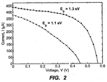
- FIG. 2 is a plot of the photovoltaic response of a depleted heterojunction solar cell as prepared above, expressed as current in mA vs voltage, with the lower curve representing cells fabricated with 0.9eV-bandgap (5.5nm) quantum dots, the middle curve representing the cells fabricated with 1.1eV-bandgap (4.3nm) quantum dots, and the upper curve representing the cells fabricated with 1.3eV-bandgap (3.7nm) quantum dots.
- FIG. 3 is a plot of external quantum efficiency (EQE) vs . wavelength and of absorption vs . wavelength, with the lower curve representing the EQE for the best-performing 1.3eV-bandgap quantum dot device and the upper curve representing the spectral absorption of the same device.
- the EQE is the ratio of extracted electrons to incident photons and the curve is also known as the incident photon conversion efficiency spectrum.
- the EQE was obtained by passing the output of a 400W Xe lamp through a monochromator and using appropriate order-sorting filters. The collimated output of the monochromator was measured through a 1.5nm aperture with a calibrated Newport 818-UV power meter.
- the measurement bandwidth was about 40nm and the intensity varied with the spectrum of the Xe lamp.
- the average intensity was 0.3mW cm -2 .
- the current-voltage response was measured with Keithley 2400 source-meters. The plot shows that at short wavelengths, the EQE reached values above 60%, while at longer wavelengths the EQE had a peak of 24%.
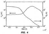
- FIG. 4 is a plot of device capacitance vs . bias voltage and of device resistance vs . bias voltage.
- the capacitance arises from the depletion layer due to charge transfer from TiO 2 to the PbS colloidal quantum dot layer.
- Capacitance-voltage measurements were performed directly on the photovoltaic devices using an Agilent 4284A LCR meter. Absorption spectroscopy was performed on a Cary 500 UV-vis-IR Scan photospectrometer. The impedance was acquired at 2kHz with a signal amplitude of 10mV, and is represented in FIG. 4 in terms of equivalent parallel resistance Rp and capacitance Cp for a device with a contact area of 0.03cm 3 .
- the plot shows that the capacitance, and its associated depletion layer distributed between the two semiconductors, persist up to a bias of 0.6V, close to the observed open-circuit voltage value. This is a direct indication of the presence of a built-in field that efficiently drives the separation of photogenerated carriers.
- This example illustrates the preparation and use of nanoparticles containing a quantum dot core, an inner shell of cations and an outer shell of anions, within the scope of the present invention.
- colloidal quantum dots capped with oleic acid ligands were synthesized and stripped of their oleate ligands, in the manner described in Example 1. These quantum dots were prepared with an excess of Pb during synthesis, resulting in a lead-rich bulk composition but with sulfur atoms on their surfaces, either from nonpolar ⁇ 100 ⁇ and ⁇ 110 ⁇ or polar ⁇ 111 ⁇ facets in their crystal structure. To form the inner shell of Cd cations over these PbS cores, the nanoparticles were treated with a solution of CdCl 2 -tetradecylphosphonic acid-oleylamine (CdCl 2 -TDPA-OLA).
- CdCl 2 -TDPA-OLA CdCl 2 -tetradecylphosphonic acid-oleylamine
- Photovoltaic devices utilizing these dual-shell-passivated quantum dots were fabricated in the same manner as described in Example 1 above.
- a scanning electron micrograph showed that the quantum dot layer was approximately 300nm in thickness and was free of the voids and cracks that often occur in films made from layer-by-layer deposition.
- Absorption spectra of the devices were obtained in a double pass by including reflection from the Au top contact.
- the spectra of devices made using 9, 11, and 13 quantum dot layers are shown in FIG. 5 , which also includes corresponding spectra from the bare FTO/TiO 2 substrate.
- the absorption peak at 950nm is the excitonic peak of the PbS quantum dots. This indicates that quantum confinement of the core quantum dots was preserved in the shelled form.
- a reduction in interparticle distance is suggested by the red-shift ( ⁇ 100meV) of the excitonic peak in the final film as compared to the excitonic peak of dots in solution.
- the device Upon exposure to 100 mW/cm 2 solar illumination, the device showed an open circuit voltage ( V oc ) of 0.45V, a short-circuit current density ( J sc ) of 21.8mA/cm 2 , and a fill factor ( FF ) of 59%, yielding a power conversion efficiency ⁇ of 5.76%. Integration of the net absorption of the quantum dot film over the AM1.5G spectrum indicates that a film having 100% quantum efficiency would have achieved a circuit current density ( J sc ) of 24.4mA/cm 2 .
- the doping density and carrier lifetime of the dual-shell-passivated quantum dot films were determined by capacitance-voltage (C-V) and V oc decay analyses, respectively.
- C-V analysis showed that doping was a full order of magnitude lower than in the lowest-doped organic ligand PbS and PbSe quantum dot films, and the carrier lifetime ⁇ , which is shown in FIG. 6 , was approximately twice as long as that of a control device made using a bidentate organic ligand (3-mercaptopropionic acid, also shown in FIG. 6 ), reaching a remarkably long lifetime of over 40 ⁇ sec even under full solar 100 mW/cm 2 illumination.
- FIG. 7 is a plot of current density vs . voltage, comparing a layer of dual-shell-passivated quantum dots in accordance with the invention with quantum dots bearing 3-mercaptopropionic acid ligands, each shown both fresh (immediately after fabrication) and after ten days of storage under ambient conditions on a laboratory bench.
- the dual-shell-passivated quantum dots showed no significant change in performance over the ten-day period, while the organic ligand-capped quantum dots underwent a complete loss of efficiency over the same period.
- HTAC hexatrimethylammonium chloride
- CTAB cetyltrimethylammonium bromide
- TBAI tetrabutylammonium iodide
- TBAT tetrabutylammonium thiocyanate
Landscapes
- Chemical & Material Sciences (AREA)
- Engineering & Computer Science (AREA)
- Materials Engineering (AREA)
- Organic Chemistry (AREA)
- Inorganic Chemistry (AREA)
- Photovoltaic Devices (AREA)
Applications Claiming Priority (4)
| Application Number | Priority Date | Filing Date | Title |
|---|---|---|---|
| US32145010P | 2010-04-06 | 2010-04-06 | |
| US33465010P | 2010-05-14 | 2010-05-14 | |
| US12/890,797 US9382474B2 (en) | 2010-04-06 | 2010-09-27 | Photovoltaic devices with depleted heterojunctions and shell-passivated nanoparticles |
| PCT/US2011/030074 WO2011126778A1 (en) | 2010-04-06 | 2011-03-25 | Photovoltaic devices with depleted heterojunctions and shell-passivated nanoparticles |
Publications (2)
| Publication Number | Publication Date |
|---|---|
| EP2556131A1 EP2556131A1 (en) | 2013-02-13 |
| EP2556131B1 true EP2556131B1 (en) | 2016-10-12 |
Family
ID=44708204
Family Applications (1)
| Application Number | Title | Priority Date | Filing Date |
|---|---|---|---|
| EP11711741.6A Active EP2556131B1 (en) | 2010-04-06 | 2011-03-25 | Photovoltaic devices with depleted heterojunctions and shell-passivated nanoparticles |
Country Status (11)
| Country | Link |
|---|---|
| US (2) | US9382474B2 (https=) |
| EP (1) | EP2556131B1 (https=) |
| JP (2) | JP6117693B2 (https=) |
| KR (1) | KR101894408B1 (https=) |
| CN (2) | CN106167704B (https=) |
| AU (1) | AU2011238678A1 (https=) |
| BR (1) | BR112012025386A2 (https=) |
| CA (2) | CA3061443C (https=) |
| RU (1) | RU2012131848A (https=) |
| SG (1) | SG184407A1 (https=) |
| WO (1) | WO2011126778A1 (https=) |
Families Citing this family (29)
| Publication number | Priority date | Publication date | Assignee | Title |
|---|---|---|---|---|
| US9382474B2 (en) | 2010-04-06 | 2016-07-05 | The Governing Council Of The University Of Toronto | Photovoltaic devices with depleted heterojunctions and shell-passivated nanoparticles |
| US9030189B2 (en) | 2011-08-28 | 2015-05-12 | Edward Hartley Sargent | Quantum dot photo-field-effect transistor |
| US8962378B2 (en) * | 2012-07-16 | 2015-02-24 | The Boeing Company | Photodiode and method for making the same |
| WO2014103609A1 (ja) * | 2012-12-26 | 2014-07-03 | 富士フイルム株式会社 | 半導体膜、半導体膜の製造方法、太陽電池、発光ダイオード、薄膜トランジスタ、および、電子デバイス |
| CA2899045A1 (en) * | 2013-02-21 | 2014-08-28 | The Governing Council Of The University Of Toronto | Photovoltaic devices with plasmonic nanoparticles |
| RU2532690C1 (ru) * | 2013-04-19 | 2014-11-10 | федеральное государственное автономное образовательное учреждение высшего образования "Санкт-Петербургский национальный исследовательский университет информационных технологий, механики и оптики" | Способ создания фотовольтаических ячеек на основе гибридного нанокомпозитного материала |
| WO2015075564A2 (en) | 2013-10-04 | 2015-05-28 | King Abdullah University Of Science And Technology | System and method for making quantum dots |
| PL3084854T3 (pl) | 2013-12-17 | 2020-07-13 | Oxford University Innovation Limited | Urządzenie fotowoltaiczne zawierające perowskit halogenku metalu i środek pasywujący |
| US9099663B1 (en) * | 2014-04-21 | 2015-08-04 | Massachusetts Institute Of Technology | Quantum dot solar cells with band alignment engineering |
| CA2948486A1 (en) * | 2014-05-09 | 2015-11-12 | Massachusetts Institute Of Technology | Energy level modification of nanocrystals through ligand exchange |
| CN104393069B (zh) * | 2014-10-24 | 2017-01-18 | 颜步一 | 二氧化钛纳米晶体颗粒及其制备方法以及在太阳能电池上的应用 |
| EP3116043B1 (en) * | 2015-07-10 | 2021-09-15 | Fundació Institut de Ciències Fotòniques | A photovoltaic material and use of it in a photovoltaic device |
| KR102446410B1 (ko) * | 2015-09-17 | 2022-09-22 | 삼성전자주식회사 | 광전소자 및 이를 포함하는 전자장치 |
| KR102608507B1 (ko) * | 2016-08-30 | 2023-12-01 | 삼성디스플레이 주식회사 | 표시장치 및 그 제조방법 |
| CN106701060A (zh) * | 2016-12-22 | 2017-05-24 | Tcl集团股份有限公司 | 钝化量子点膜及其制备方法 |
| WO2018152494A1 (en) | 2017-02-17 | 2018-08-23 | Nutech Ventures | Passivation of defects in perovskite materials for improved solar cell efficiency and stability |
| CN109988573A (zh) * | 2017-12-29 | 2019-07-09 | Tcl集团股份有限公司 | 复合量子点、量子点固态膜及其应用 |
| CN108893103A (zh) * | 2018-07-11 | 2018-11-27 | 苏州星烁纳米科技有限公司 | 包覆量子点的方法及其制备的产品 |
| US20200067002A1 (en) * | 2018-08-23 | 2020-02-27 | Nanoco 2D Materials Limited | Photodetectors Based on Two-Dimensional Quantum Dots |
| EP3852151A4 (en) * | 2018-09-12 | 2022-06-15 | NS Materials Inc. | INFRARED SENSOR AND METHOD OF MANUFACTURE THEREOF |
| US11538948B2 (en) | 2019-06-26 | 2022-12-27 | University Of South Carolina | Quantum dot photovoltaic junctions |
| CN110350045B (zh) * | 2019-07-24 | 2024-05-07 | 中国科学院重庆绿色智能技术研究院 | PbS量子点Si-APD红外探测器及其制备方法 |
| KR20210048289A (ko) * | 2019-10-23 | 2021-05-03 | 삼성전자주식회사 | 수광 소자 |
| CN115477935A (zh) * | 2021-05-31 | 2022-12-16 | Tcl科技集团股份有限公司 | 一种量子点薄膜及其制备方法、量子点发光二极管与显示装置 |
| FR3124799A1 (fr) * | 2021-06-30 | 2023-01-06 | Aledia | Nanoparticule émettrice de lumière et protégée, son procédé de fabrication et son application pour les convertisseurs de rayonnement de dispositif optoélectronique |
| CN114108037B (zh) * | 2021-11-22 | 2023-03-03 | 湖南大学 | 光电阴极及其制备方法、金属锂提取方法及提取装置 |
| CN114188490B (zh) * | 2021-12-10 | 2024-03-12 | 京东方科技集团股份有限公司 | 量子点-半导体复合膜层及其制备方法、量子点发光器件 |
| CN115784630B (zh) * | 2022-11-15 | 2024-03-29 | 湖北大学 | 一种异质结复合薄膜及其制备方法和应用、甲烷气体传感器 |
| CN116814244A (zh) * | 2023-06-28 | 2023-09-29 | 电子科技大学 | 一种铅族核壳结构量子点及其制备方法 |
Family Cites Families (26)
| Publication number | Priority date | Publication date | Assignee | Title |
|---|---|---|---|---|
| JPS5653209A (en) | 1979-10-01 | 1981-05-12 | Kanebo Ltd | Composite acrylic fiber having water absorption and its preparation |
| US6198092B1 (en) * | 1998-08-19 | 2001-03-06 | The Trustees Of Princeton University | Stacked organic photosensitive optoelectronic devices with an electrically parallel configuration |
| EP1176646A1 (en) * | 2000-07-28 | 2002-01-30 | Ecole Polytechnique Féderale de Lausanne (EPFL) | Solid state heterojunction and solid state sensitized photovoltaic cell |
| JP2006501640A (ja) | 2002-08-13 | 2006-01-12 | アグフア−ゲヴエルト | 金属カルコゲニドナノ−粒子を用いて分光増感されたナノ−多孔質金属酸化物半導体 |
| US20050126628A1 (en) | 2002-09-05 | 2005-06-16 | Nanosys, Inc. | Nanostructure and nanocomposite based compositions and photovoltaic devices |
| WO2004066361A2 (en) * | 2003-01-22 | 2004-08-05 | The Board Of Trustees Of The University Of Arkansas | Monodisperse core/shell and other complex structured nanocrystals and methods of preparing the same |
| JP2005159168A (ja) | 2003-11-27 | 2005-06-16 | Kyocera Corp | 光電変換装置およびその製造方法 |
| CN100477289C (zh) * | 2004-01-20 | 2009-04-08 | 瑟雷姆技术公司 | 具有外延生长量子点材料的太阳能电池 |
| GB0409877D0 (en) | 2004-04-30 | 2004-06-09 | Univ Manchester | Preparation of nanoparticle materials |
| JP4639107B2 (ja) | 2005-03-31 | 2011-02-23 | 富士通株式会社 | 半導体レーザ及びその製造方法 |
| WO2006110341A2 (en) * | 2005-04-01 | 2006-10-19 | North Carolina State University | Nano-structured photovoltaic solar cells and related methods |
| WO2006134599A1 (en) * | 2005-06-15 | 2006-12-21 | Yissum Research Development Company Of The Hebrew University Of Jerusalem | Iii-v semiconductor core-heteroshell nanocrystals |
| US7385231B2 (en) * | 2005-08-31 | 2008-06-10 | Fujifilmcorporation | Porous thin-film-deposition substrate, electron emitting element, methods of producing them, and switching element and display element |
| TWI273719B (en) | 2005-12-30 | 2007-02-11 | Ind Tech Res Inst | Nanocrystal and photovoltaics applying the same |
| EP1997163A2 (en) | 2006-03-23 | 2008-12-03 | Solexant Corp. | Photovoltaic device containing nanoparticle sensitized carbon nanotubes |
| EP2020967B1 (en) | 2006-05-12 | 2020-09-23 | Cardinal Health Switzerland 515 GmbH | Baloon expandable bioabsorbable drug eluting stent |
| US9105776B2 (en) | 2006-05-15 | 2015-08-11 | Stion Corporation | Method and structure for thin film photovoltaic materials using semiconductor materials |
| CN101400512B (zh) | 2006-05-15 | 2013-10-30 | 思阳公司 | 利用半导体材料的用于薄膜光生伏打材料的方法和结构 |
| US8866007B2 (en) * | 2006-06-07 | 2014-10-21 | California Institute Of Technology | Plasmonic photovoltaics |
| US7968792B2 (en) | 2007-03-05 | 2011-06-28 | Seagate Technology Llc | Quantum dot sensitized wide bandgap semiconductor photovoltaic devices & methods of fabricating same |
| KR100841186B1 (ko) * | 2007-03-26 | 2008-06-24 | 삼성전자주식회사 | 다층 쉘 구조의 나노결정 및 그의 제조방법 |
| WO2009026141A1 (en) * | 2007-08-17 | 2009-02-26 | University Of Florida Research Foundation, Inc. | Supercrystalline colloidal particles and method of production |
| KR101460395B1 (ko) | 2007-12-13 | 2014-11-21 | 테크니온 리서치 엔드 디벨로프먼트 화운데이션 엘티디. | 4-6족 반도체 코어-쉘 나노결정을 포함하는 광기전 셀 |
| WO2010018490A2 (en) | 2008-08-12 | 2010-02-18 | Nxp B.V. | A photovoltaic cell and a method of manufacturing the same |
| KR101060014B1 (ko) * | 2008-08-28 | 2011-08-26 | 한국표준과학연구원 | 양자점 태양광 소자 및 그 제조방법 |
| US9382474B2 (en) | 2010-04-06 | 2016-07-05 | The Governing Council Of The University Of Toronto | Photovoltaic devices with depleted heterojunctions and shell-passivated nanoparticles |
-
2010
- 2010-09-27 US US12/890,797 patent/US9382474B2/en active Active
-
2011
- 2011-03-25 BR BR112012025386A patent/BR112012025386A2/pt not_active Application Discontinuation
- 2011-03-25 CN CN201610694633.6A patent/CN106167704B/zh not_active Expired - Fee Related
- 2011-03-25 EP EP11711741.6A patent/EP2556131B1/en active Active
- 2011-03-25 AU AU2011238678A patent/AU2011238678A1/en not_active Abandoned
- 2011-03-25 SG SG2012073268A patent/SG184407A1/en unknown
- 2011-03-25 KR KR1020127029025A patent/KR101894408B1/ko not_active Expired - Fee Related
- 2011-03-25 RU RU2012131848/28A patent/RU2012131848A/ru not_active Application Discontinuation
- 2011-03-25 CA CA3061443A patent/CA3061443C/en active Active
- 2011-03-25 CA CA2795719A patent/CA2795719C/en active Active
- 2011-03-25 JP JP2013503781A patent/JP6117693B2/ja not_active Expired - Fee Related
- 2011-03-25 CN CN201180017884.6A patent/CN102859710B/zh not_active Expired - Fee Related
- 2011-03-25 WO PCT/US2011/030074 patent/WO2011126778A1/en not_active Ceased
-
2016
- 2016-06-24 US US15/192,361 patent/US10784388B2/en active Active
- 2016-11-18 JP JP2016225169A patent/JP6360130B2/ja not_active Expired - Fee Related
Non-Patent Citations (2)
| Title |
|---|
| HYO JOONG LEE ET AL: "Multilayered Semiconductor (CdS/CdSe/ZnS)-Sensitized TiO 2 Mesoporous Solar Cells: All Prepared by Successive Ionic Layer Adsorption and Reaction Processes", CHEMISTRY OF MATERIALS, vol. 22, no. 19, 8 September 2010 (2010-09-08), pages 5636 - 5643, XP055108098, ISSN: 0897-4756, DOI: 10.1021/cm102024s * |
| SHINAE JUN ET AL: "Interfused semiconductor nanocrystals: brilliant blue photoluminescence and electroluminescence", CHEMICAL COMMUNICATIONS, no. 36, 1 January 2005 (2005-01-01), pages 4616 - 4618, XP055171388, ISSN: 1359-7345, DOI: 10.1039/b509196a * |
Also Published As
| Publication number | Publication date |
|---|---|
| US10784388B2 (en) | 2020-09-22 |
| CA3061443A1 (en) | 2011-10-13 |
| CN102859710B (zh) | 2016-10-19 |
| JP2013524530A (ja) | 2013-06-17 |
| KR101894408B1 (ko) | 2018-09-03 |
| JP6360130B2 (ja) | 2018-07-18 |
| CA3061443C (en) | 2022-04-12 |
| US20110240106A1 (en) | 2011-10-06 |
| CA2795719C (en) | 2020-01-14 |
| US20160372616A1 (en) | 2016-12-22 |
| BR112012025386A2 (pt) | 2016-06-28 |
| CN102859710A (zh) | 2013-01-02 |
| CA2795719A1 (en) | 2011-10-13 |
| CN106167704A (zh) | 2016-11-30 |
| CN106167704B (zh) | 2020-09-04 |
| JP2017085113A (ja) | 2017-05-18 |
| RU2012131848A (ru) | 2014-01-27 |
| WO2011126778A1 (en) | 2011-10-13 |
| US9382474B2 (en) | 2016-07-05 |
| AU2011238678A1 (en) | 2012-10-25 |
| JP6117693B2 (ja) | 2017-04-19 |
| KR20130098146A (ko) | 2013-09-04 |
| SG184407A1 (en) | 2012-11-29 |
| EP2556131A1 (en) | 2013-02-13 |
Similar Documents
| Publication | Publication Date | Title |
|---|---|---|
| EP2556131B1 (en) | Photovoltaic devices with depleted heterojunctions and shell-passivated nanoparticles | |
| Lei et al. | Review of recent progress in antimony chalcogenide‐based solar cells: materials and devices | |
| US7632701B2 (en) | Thin film solar cells by selenization sulfurization using diethyl selenium as a selenium precursor | |
| Jean et al. | ZnO nanowire arrays for enhanced photocurrent in PbS quantum dot solar cells | |
| JP5782117B2 (ja) | 傾斜再結合層によって分離された多重接合を有する光起電デバイス | |
| Jang et al. | Monolithic tandem solar cells comprising electrodeposited CuInSe 2 and perovskite solar cells with a nanoparticulate ZnO buffer layer | |
| Fan et al. | Delayed annealing treatment for high-quality CuSCN: Exploring its impact on bifacial semitransparent nip planar perovskite solar cells | |
| US20170243999A1 (en) | Solar cell | |
| Sie et al. | Pb5Sb8S17 quantum dot‐sensitized solar cells with an efficiency of 6% under 0.05 sun: T heoretical and experimental studies | |
| CN103229313A (zh) | 作为无机太阳能电池窗口层的有机半导体 | |
| Lim et al. | Enhancing the device performance of Sb 2 S 3-sensitized heterojunction solar cells by embedding Au nanoparticles in the hole-conducting polymer layer | |
| Zhao et al. | Improving the performance of Sb2Se3 sensitized solar cells with a versatile CdSe layer modification | |
| Yakovleva et al. | Back contact passivation with Ga-grading in narrow bandgap (Ag, Cu)(In, Ga) Se 2 bifacial solar cells on In 2 O 3: Sn back contact | |
| Sung et al. | Effect of Ultrathin Al 2 O 3 Layer on TiO 2 Surface in CdS/CdSe Co-Sensitized Quantum Dot Solar Cells | |
| HK1181784B (en) | Photovoltaic devices with depleted heterojunctions and shell-passivated nanoparticles | |
| KR20170114853A (ko) | 태양전지용 광활성층, 이를 포함하는 태양전지, 및 이들의 제조방법 | |
| Subedi | Development and Application of Transparent P-type Back Contact Layers for Bifacial CdTe Solar Cells | |
| Bailie | Polycrystalline Tandem Photovoltaics | |
| 김재익 | Enhancing the Performance and Stability of Electrode Materials for Photovoltaic Devices | |
| KR20170124513A (ko) | 태양전지용 광활성층, 이를 포함하는 태양전지, 및 이들의 제조방법 | |
| Shishehbori et al. | The investigation of the influence of back contact metal and ligand exchanging on the air stability of ambient processed schottky Photovoltaic Cells Based on PbSe CQDs | |
| Loucif Narimane | Study of perovskite based tandem solar cells |
Legal Events
| Date | Code | Title | Description |
|---|---|---|---|
| PUAI | Public reference made under article 153(3) epc to a published international application that has entered the european phase |
Free format text: ORIGINAL CODE: 0009012 |
|
| 17P | Request for examination filed |
Effective date: 20121002 |
|
| AK | Designated contracting states |
Kind code of ref document: A1 Designated state(s): AL AT BE BG CH CY CZ DE DK EE ES FI FR GB GR HR HU IE IS IT LI LT LU LV MC MK MT NL NO PL PT RO RS SE SI SK SM TR |
|
| RIN1 | Information on inventor provided before grant (corrected) |
Inventor name: KRAMER, ILLAN Inventor name: BARKHOUSE, AARON Inventor name: TANG, JIANG Inventor name: DEBNATH, RATAN Inventor name: SARGENT, EDWARD H. Inventor name: PATTANTYUS-ABRAHAM, ANDRAS Inventor name: WANG, XIHUA Inventor name: GERASIMOS, KONSTANTATOS |
|
| RIN1 | Information on inventor provided before grant (corrected) |
Inventor name: SARGENT, EDWARD H. Inventor name: TANG, JIANG Inventor name: DEBNATH, RATAN Inventor name: KRAMER, ILLAN Inventor name: PATTANTYUS-ABRAHAM, ANDRAS Inventor name: GERASIMOS, KONSTANTATOS Inventor name: BARKHOUSE, AARON Inventor name: WANG, XIHUA |
|
| DAX | Request for extension of the european patent (deleted) | ||
| REG | Reference to a national code |
Ref country code: HK Ref legal event code: DE Ref document number: 1181784 Country of ref document: HK |
|
| 17Q | First examination report despatched |
Effective date: 20140321 |
|
| GRAP | Despatch of communication of intention to grant a patent |
Free format text: ORIGINAL CODE: EPIDOSNIGR1 |
|
| INTG | Intention to grant announced |
Effective date: 20151120 |
|
| GRAJ | Information related to disapproval of communication of intention to grant by the applicant or resumption of examination proceedings by the epo deleted |
Free format text: ORIGINAL CODE: EPIDOSDIGR1 |
|
| GRAP | Despatch of communication of intention to grant a patent |
Free format text: ORIGINAL CODE: EPIDOSNIGR1 |
|
| GRAP | Despatch of communication of intention to grant a patent |
Free format text: ORIGINAL CODE: EPIDOSNIGR1 |
|
| INTG | Intention to grant announced |
Effective date: 20160506 |
|
| GRAS | Grant fee paid |
Free format text: ORIGINAL CODE: EPIDOSNIGR3 |
|
| GRAA | (expected) grant |
Free format text: ORIGINAL CODE: 0009210 |
|
| AK | Designated contracting states |
Kind code of ref document: B1 Designated state(s): AL AT BE BG CH CY CZ DE DK EE ES FI FR GB GR HR HU IE IS IT LI LT LU LV MC MK MT NL NO PL PT RO RS SE SI SK SM TR |
|
| REG | Reference to a national code |
Ref country code: GB Ref legal event code: FG4D |
|
| REG | Reference to a national code |
Ref country code: CH Ref legal event code: EP |
|
| REG | Reference to a national code |
Ref country code: AT Ref legal event code: REF Ref document number: 836514 Country of ref document: AT Kind code of ref document: T Effective date: 20161015 |
|
| REG | Reference to a national code |
Ref country code: IE Ref legal event code: FG4D |
|
| REG | Reference to a national code |
Ref country code: DE Ref legal event code: R096 Ref document number: 602011031172 Country of ref document: DE |
|
| REG | Reference to a national code |
Ref country code: LT Ref legal event code: MG4D |
|
| REG | Reference to a national code |
Ref country code: FR Ref legal event code: PLFP Year of fee payment: 7 |
|
| REG | Reference to a national code |
Ref country code: NL Ref legal event code: MP Effective date: 20161012 |
|
| PG25 | Lapsed in a contracting state [announced via postgrant information from national office to epo] |
Ref country code: LV Free format text: LAPSE BECAUSE OF FAILURE TO SUBMIT A TRANSLATION OF THE DESCRIPTION OR TO PAY THE FEE WITHIN THE PRESCRIBED TIME-LIMIT Effective date: 20161012 |
|
| REG | Reference to a national code |
Ref country code: AT Ref legal event code: MK05 Ref document number: 836514 Country of ref document: AT Kind code of ref document: T Effective date: 20161012 |
|
| PG25 | Lapsed in a contracting state [announced via postgrant information from national office to epo] |
Ref country code: LT Free format text: LAPSE BECAUSE OF FAILURE TO SUBMIT A TRANSLATION OF THE DESCRIPTION OR TO PAY THE FEE WITHIN THE PRESCRIBED TIME-LIMIT Effective date: 20161012 Ref country code: GR Free format text: LAPSE BECAUSE OF FAILURE TO SUBMIT A TRANSLATION OF THE DESCRIPTION OR TO PAY THE FEE WITHIN THE PRESCRIBED TIME-LIMIT Effective date: 20170113 Ref country code: NO Free format text: LAPSE BECAUSE OF FAILURE TO SUBMIT A TRANSLATION OF THE DESCRIPTION OR TO PAY THE FEE WITHIN THE PRESCRIBED TIME-LIMIT Effective date: 20170112 Ref country code: SE Free format text: LAPSE BECAUSE OF FAILURE TO SUBMIT A TRANSLATION OF THE DESCRIPTION OR TO PAY THE FEE WITHIN THE PRESCRIBED TIME-LIMIT Effective date: 20161012 |
|
| PG25 | Lapsed in a contracting state [announced via postgrant information from national office to epo] |
Ref country code: NL Free format text: LAPSE BECAUSE OF FAILURE TO SUBMIT A TRANSLATION OF THE DESCRIPTION OR TO PAY THE FEE WITHIN THE PRESCRIBED TIME-LIMIT Effective date: 20161012 Ref country code: IS Free format text: LAPSE BECAUSE OF FAILURE TO SUBMIT A TRANSLATION OF THE DESCRIPTION OR TO PAY THE FEE WITHIN THE PRESCRIBED TIME-LIMIT Effective date: 20170212 Ref country code: BE Free format text: LAPSE BECAUSE OF FAILURE TO SUBMIT A TRANSLATION OF THE DESCRIPTION OR TO PAY THE FEE WITHIN THE PRESCRIBED TIME-LIMIT Effective date: 20161012 Ref country code: PL Free format text: LAPSE BECAUSE OF FAILURE TO SUBMIT A TRANSLATION OF THE DESCRIPTION OR TO PAY THE FEE WITHIN THE PRESCRIBED TIME-LIMIT Effective date: 20161012 Ref country code: ES Free format text: LAPSE BECAUSE OF FAILURE TO SUBMIT A TRANSLATION OF THE DESCRIPTION OR TO PAY THE FEE WITHIN THE PRESCRIBED TIME-LIMIT Effective date: 20161012 Ref country code: AT Free format text: LAPSE BECAUSE OF FAILURE TO SUBMIT A TRANSLATION OF THE DESCRIPTION OR TO PAY THE FEE WITHIN THE PRESCRIBED TIME-LIMIT Effective date: 20161012 Ref country code: RS Free format text: LAPSE BECAUSE OF FAILURE TO SUBMIT A TRANSLATION OF THE DESCRIPTION OR TO PAY THE FEE WITHIN THE PRESCRIBED TIME-LIMIT Effective date: 20161012 Ref country code: HR Free format text: LAPSE BECAUSE OF FAILURE TO SUBMIT A TRANSLATION OF THE DESCRIPTION OR TO PAY THE FEE WITHIN THE PRESCRIBED TIME-LIMIT Effective date: 20161012 Ref country code: FI Free format text: LAPSE BECAUSE OF FAILURE TO SUBMIT A TRANSLATION OF THE DESCRIPTION OR TO PAY THE FEE WITHIN THE PRESCRIBED TIME-LIMIT Effective date: 20161012 Ref country code: PT Free format text: LAPSE BECAUSE OF FAILURE TO SUBMIT A TRANSLATION OF THE DESCRIPTION OR TO PAY THE FEE WITHIN THE PRESCRIBED TIME-LIMIT Effective date: 20170213 |
|
| REG | Reference to a national code |
Ref country code: DE Ref legal event code: R097 Ref document number: 602011031172 Country of ref document: DE |
|
| PG25 | Lapsed in a contracting state [announced via postgrant information from national office to epo] |
Ref country code: DK Free format text: LAPSE BECAUSE OF FAILURE TO SUBMIT A TRANSLATION OF THE DESCRIPTION OR TO PAY THE FEE WITHIN THE PRESCRIBED TIME-LIMIT Effective date: 20161012 Ref country code: CZ Free format text: LAPSE BECAUSE OF FAILURE TO SUBMIT A TRANSLATION OF THE DESCRIPTION OR TO PAY THE FEE WITHIN THE PRESCRIBED TIME-LIMIT Effective date: 20161012 Ref country code: SK Free format text: LAPSE BECAUSE OF FAILURE TO SUBMIT A TRANSLATION OF THE DESCRIPTION OR TO PAY THE FEE WITHIN THE PRESCRIBED TIME-LIMIT Effective date: 20161012 Ref country code: EE Free format text: LAPSE BECAUSE OF FAILURE TO SUBMIT A TRANSLATION OF THE DESCRIPTION OR TO PAY THE FEE WITHIN THE PRESCRIBED TIME-LIMIT Effective date: 20161012 Ref country code: RO Free format text: LAPSE BECAUSE OF FAILURE TO SUBMIT A TRANSLATION OF THE DESCRIPTION OR TO PAY THE FEE WITHIN THE PRESCRIBED TIME-LIMIT Effective date: 20161012 |
|
| PLBE | No opposition filed within time limit |
Free format text: ORIGINAL CODE: 0009261 |
|
| STAA | Information on the status of an ep patent application or granted ep patent |
Free format text: STATUS: NO OPPOSITION FILED WITHIN TIME LIMIT |
|
| PG25 | Lapsed in a contracting state [announced via postgrant information from national office to epo] |
Ref country code: SM Free format text: LAPSE BECAUSE OF FAILURE TO SUBMIT A TRANSLATION OF THE DESCRIPTION OR TO PAY THE FEE WITHIN THE PRESCRIBED TIME-LIMIT Effective date: 20161012 Ref country code: IT Free format text: LAPSE BECAUSE OF FAILURE TO SUBMIT A TRANSLATION OF THE DESCRIPTION OR TO PAY THE FEE WITHIN THE PRESCRIBED TIME-LIMIT Effective date: 20161012 Ref country code: BG Free format text: LAPSE BECAUSE OF FAILURE TO SUBMIT A TRANSLATION OF THE DESCRIPTION OR TO PAY THE FEE WITHIN THE PRESCRIBED TIME-LIMIT Effective date: 20170112 |
|
| 26N | No opposition filed |
Effective date: 20170713 |
|
| REG | Reference to a national code |
Ref country code: CH Ref legal event code: PL |
|
| REG | Reference to a national code |
Ref country code: HK Ref legal event code: GR Ref document number: 1181784 Country of ref document: HK |
|
| PG25 | Lapsed in a contracting state [announced via postgrant information from national office to epo] |
Ref country code: MC Free format text: LAPSE BECAUSE OF FAILURE TO SUBMIT A TRANSLATION OF THE DESCRIPTION OR TO PAY THE FEE WITHIN THE PRESCRIBED TIME-LIMIT Effective date: 20161012 Ref country code: SI Free format text: LAPSE BECAUSE OF FAILURE TO SUBMIT A TRANSLATION OF THE DESCRIPTION OR TO PAY THE FEE WITHIN THE PRESCRIBED TIME-LIMIT Effective date: 20161012 |
|
| REG | Reference to a national code |
Ref country code: IE Ref legal event code: MM4A |
|
| PG25 | Lapsed in a contracting state [announced via postgrant information from national office to epo] |
Ref country code: LU Free format text: LAPSE BECAUSE OF NON-PAYMENT OF DUE FEES Effective date: 20170325 |
|
| REG | Reference to a national code |
Ref country code: FR Ref legal event code: PLFP Year of fee payment: 8 |
|
| PG25 | Lapsed in a contracting state [announced via postgrant information from national office to epo] |
Ref country code: CH Free format text: LAPSE BECAUSE OF NON-PAYMENT OF DUE FEES Effective date: 20170331 Ref country code: IE Free format text: LAPSE BECAUSE OF NON-PAYMENT OF DUE FEES Effective date: 20170325 Ref country code: LI Free format text: LAPSE BECAUSE OF NON-PAYMENT OF DUE FEES Effective date: 20170331 |
|
| PG25 | Lapsed in a contracting state [announced via postgrant information from national office to epo] |
Ref country code: MT Free format text: LAPSE BECAUSE OF NON-PAYMENT OF DUE FEES Effective date: 20170325 |
|
| PG25 | Lapsed in a contracting state [announced via postgrant information from national office to epo] |
Ref country code: HU Free format text: LAPSE BECAUSE OF FAILURE TO SUBMIT A TRANSLATION OF THE DESCRIPTION OR TO PAY THE FEE WITHIN THE PRESCRIBED TIME-LIMIT; INVALID AB INITIO Effective date: 20110325 |
|
| PG25 | Lapsed in a contracting state [announced via postgrant information from national office to epo] |
Ref country code: CY Free format text: LAPSE BECAUSE OF NON-PAYMENT OF DUE FEES Effective date: 20161012 |
|
| PG25 | Lapsed in a contracting state [announced via postgrant information from national office to epo] |
Ref country code: MK Free format text: LAPSE BECAUSE OF FAILURE TO SUBMIT A TRANSLATION OF THE DESCRIPTION OR TO PAY THE FEE WITHIN THE PRESCRIBED TIME-LIMIT Effective date: 20161012 |
|
| PG25 | Lapsed in a contracting state [announced via postgrant information from national office to epo] |
Ref country code: TR Free format text: LAPSE BECAUSE OF FAILURE TO SUBMIT A TRANSLATION OF THE DESCRIPTION OR TO PAY THE FEE WITHIN THE PRESCRIBED TIME-LIMIT Effective date: 20161012 |
|
| PG25 | Lapsed in a contracting state [announced via postgrant information from national office to epo] |
Ref country code: AL Free format text: LAPSE BECAUSE OF FAILURE TO SUBMIT A TRANSLATION OF THE DESCRIPTION OR TO PAY THE FEE WITHIN THE PRESCRIBED TIME-LIMIT Effective date: 20161012 |
|
| PGFP | Annual fee paid to national office [announced via postgrant information from national office to epo] |
Ref country code: GB Payment date: 20240314 Year of fee payment: 14 |
|
| PGFP | Annual fee paid to national office [announced via postgrant information from national office to epo] |
Ref country code: FR Payment date: 20240321 Year of fee payment: 14 |
|
| GBPC | Gb: european patent ceased through non-payment of renewal fee |
Effective date: 20250325 |
|
| PG25 | Lapsed in a contracting state [announced via postgrant information from national office to epo] |
Ref country code: GB Free format text: LAPSE BECAUSE OF NON-PAYMENT OF DUE FEES Effective date: 20250325 |
|
| PG25 | Lapsed in a contracting state [announced via postgrant information from national office to epo] |
Ref country code: FR Free format text: LAPSE BECAUSE OF NON-PAYMENT OF DUE FEES Effective date: 20250331 |
|
| PGFP | Annual fee paid to national office [announced via postgrant information from national office to epo] |
Ref country code: DE Payment date: 20260325 Year of fee payment: 16 |