EP2543119B1 - Dispositifs optoélectroniques semi-polaires à base de nitrure de groupe iii sur des substrats de gan de plan m à angle de coupe entre 1 et 15 degrés ou entre -1 et -15 degrés dans la direction c - Google Patents
Dispositifs optoélectroniques semi-polaires à base de nitrure de groupe iii sur des substrats de gan de plan m à angle de coupe entre 1 et 15 degrés ou entre -1 et -15 degrés dans la direction c Download PDFInfo
- Publication number
- EP2543119B1 EP2543119B1 EP11751456.2A EP11751456A EP2543119B1 EP 2543119 B1 EP2543119 B1 EP 2543119B1 EP 11751456 A EP11751456 A EP 11751456A EP 2543119 B1 EP2543119 B1 EP 2543119B1
- Authority
- EP
- European Patent Office
- Prior art keywords
- semi
- gan
- polar
- ingan
- layers
- Prior art date
- Legal status (The legal status is an assumption and is not a legal conclusion. Google has not performed a legal analysis and makes no representation as to the accuracy of the status listed.)
- Active
Links
- 230000005693 optoelectronics Effects 0.000 title claims description 39
- 239000000758 substrate Substances 0.000 title description 15
- 239000013078 crystal Substances 0.000 claims description 79
- 229910052738 indium Inorganic materials 0.000 claims description 68
- 229910052733 gallium Inorganic materials 0.000 claims description 41
- 239000000203 mixture Substances 0.000 claims description 29
- APFVFJFRJDLVQX-UHFFFAOYSA-N indium atom Chemical compound [In] APFVFJFRJDLVQX-UHFFFAOYSA-N 0.000 claims description 26
- 238000000151 deposition Methods 0.000 claims description 22
- JMASRVWKEDWRBT-UHFFFAOYSA-N Gallium nitride Chemical compound [Ga]#N JMASRVWKEDWRBT-UHFFFAOYSA-N 0.000 claims description 21
- 238000000034 method Methods 0.000 claims description 20
- 238000004519 manufacturing process Methods 0.000 claims description 5
- 230000003746 surface roughness Effects 0.000 claims description 4
- 230000031700 light absorption Effects 0.000 claims description 3
- 230000012010 growth Effects 0.000 description 23
- 229910002704 AlGaN Inorganic materials 0.000 description 13
- 229910052782 aluminium Inorganic materials 0.000 description 9
- 238000005253 cladding Methods 0.000 description 9
- 230000010287 polarization Effects 0.000 description 9
- 230000000694 effects Effects 0.000 description 7
- 230000004888 barrier function Effects 0.000 description 6
- 239000000463 material Substances 0.000 description 6
- 230000005701 quantum confined stark effect Effects 0.000 description 6
- 238000001228 spectrum Methods 0.000 description 6
- 238000005401 electroluminescence Methods 0.000 description 5
- 238000005259 measurement Methods 0.000 description 5
- 230000003287 optical effect Effects 0.000 description 5
- 230000015572 biosynthetic process Effects 0.000 description 4
- 150000001875 compounds Chemical class 0.000 description 4
- 230000007547 defect Effects 0.000 description 4
- 230000005684 electric field Effects 0.000 description 4
- 239000004065 semiconductor Substances 0.000 description 4
- 241000894007 species Species 0.000 description 4
- 238000001312 dry etching Methods 0.000 description 3
- 238000002347 injection Methods 0.000 description 3
- 239000007924 injection Substances 0.000 description 3
- 238000001020 plasma etching Methods 0.000 description 3
- 230000003595 spectral effect Effects 0.000 description 3
- 229910052984 zinc sulfide Inorganic materials 0.000 description 3
- 229910001199 N alloy Inorganic materials 0.000 description 2
- 238000013459 approach Methods 0.000 description 2
- 125000004429 atom Chemical group 0.000 description 2
- 230000000903 blocking effect Effects 0.000 description 2
- 229910052796 boron Inorganic materials 0.000 description 2
- 230000007423 decrease Effects 0.000 description 2
- 230000001419 dependent effect Effects 0.000 description 2
- 238000013461 design Methods 0.000 description 2
- 238000005530 etching Methods 0.000 description 2
- 235000015220 hamburgers Nutrition 0.000 description 2
- 238000010438 heat treatment Methods 0.000 description 2
- 238000002248 hydride vapour-phase epitaxy Methods 0.000 description 2
- 238000010348 incorporation Methods 0.000 description 2
- 239000012212 insulator Substances 0.000 description 2
- 238000010884 ion-beam technique Methods 0.000 description 2
- 229910052751 metal Inorganic materials 0.000 description 2
- 239000002184 metal Substances 0.000 description 2
- 238000012986 modification Methods 0.000 description 2
- 230000004048 modification Effects 0.000 description 2
- 230000000877 morphologic effect Effects 0.000 description 2
- 150000004767 nitrides Chemical class 0.000 description 2
- 125000004433 nitrogen atom Chemical group N* 0.000 description 2
- 239000004038 photonic crystal Substances 0.000 description 2
- 230000002269 spontaneous effect Effects 0.000 description 2
- ZOXJGFHDIHLPTG-UHFFFAOYSA-N Boron Chemical compound [B] ZOXJGFHDIHLPTG-UHFFFAOYSA-N 0.000 description 1
- 238000003917 TEM image Methods 0.000 description 1
- 239000006096 absorbing agent Substances 0.000 description 1
- XAGFODPZIPBFFR-UHFFFAOYSA-N aluminium Chemical compound [Al] XAGFODPZIPBFFR-UHFFFAOYSA-N 0.000 description 1
- 230000003466 anti-cipated effect Effects 0.000 description 1
- 230000005540 biological transmission Effects 0.000 description 1
- 238000005229 chemical vapour deposition Methods 0.000 description 1
- 230000001427 coherent effect Effects 0.000 description 1
- 238000005520 cutting process Methods 0.000 description 1
- 238000011161 development Methods 0.000 description 1
- 239000003989 dielectric material Substances 0.000 description 1
- 239000002019 doping agent Substances 0.000 description 1
- 238000001194 electroluminescence spectrum Methods 0.000 description 1
- 238000005516 engineering process Methods 0.000 description 1
- 238000005286 illumination Methods 0.000 description 1
- 238000003384 imaging method Methods 0.000 description 1
- 239000012535 impurity Substances 0.000 description 1
- 238000009616 inductively coupled plasma Methods 0.000 description 1
- 238000000608 laser ablation Methods 0.000 description 1
- 230000004807 localization Effects 0.000 description 1
- 238000004020 luminiscence type Methods 0.000 description 1
- 238000013507 mapping Methods 0.000 description 1
- 238000001465 metallisation Methods 0.000 description 1
- 238000001451 molecular beam epitaxy Methods 0.000 description 1
- 230000003071 parasitic effect Effects 0.000 description 1
- 238000000206 photolithography Methods 0.000 description 1
- 238000005424 photoluminescence Methods 0.000 description 1
- 230000008569 process Effects 0.000 description 1
- 238000012545 processing Methods 0.000 description 1
- 230000006798 recombination Effects 0.000 description 1
- 238000005215 recombination Methods 0.000 description 1
- 230000009467 reduction Effects 0.000 description 1
- 230000004044 response Effects 0.000 description 1
- 239000000243 solution Substances 0.000 description 1
- 239000000126 substance Substances 0.000 description 1
- 238000003631 wet chemical etching Methods 0.000 description 1
Images


Classifications
-
- H—ELECTRICITY
- H01—ELECTRIC ELEMENTS
- H01S—DEVICES USING THE PROCESS OF LIGHT AMPLIFICATION BY STIMULATED EMISSION OF RADIATION [LASER] TO AMPLIFY OR GENERATE LIGHT; DEVICES USING STIMULATED EMISSION OF ELECTROMAGNETIC RADIATION IN WAVE RANGES OTHER THAN OPTICAL
- H01S5/00—Semiconductor lasers
- H01S5/30—Structure or shape of the active region; Materials used for the active region
- H01S5/32—Structure or shape of the active region; Materials used for the active region comprising PN junctions, e.g. hetero- or double- heterostructures
- H01S5/3202—Structure or shape of the active region; Materials used for the active region comprising PN junctions, e.g. hetero- or double- heterostructures grown on specifically orientated substrates, or using orientation dependent growth
-
- H—ELECTRICITY
- H01—ELECTRIC ELEMENTS
- H01S—DEVICES USING THE PROCESS OF LIGHT AMPLIFICATION BY STIMULATED EMISSION OF RADIATION [LASER] TO AMPLIFY OR GENERATE LIGHT; DEVICES USING STIMULATED EMISSION OF ELECTROMAGNETIC RADIATION IN WAVE RANGES OTHER THAN OPTICAL
- H01S5/00—Semiconductor lasers
-
- B—PERFORMING OPERATIONS; TRANSPORTING
- B82—NANOTECHNOLOGY
- B82Y—SPECIFIC USES OR APPLICATIONS OF NANOSTRUCTURES; MEASUREMENT OR ANALYSIS OF NANOSTRUCTURES; MANUFACTURE OR TREATMENT OF NANOSTRUCTURES
- B82Y20/00—Nanooptics, e.g. quantum optics or photonic crystals
-
- H—ELECTRICITY
- H01—ELECTRIC ELEMENTS
- H01L—SEMICONDUCTOR DEVICES NOT COVERED BY CLASS H10
- H01L21/00—Processes or apparatus adapted for the manufacture or treatment of semiconductor or solid state devices or of parts thereof
- H01L21/02—Manufacture or treatment of semiconductor devices or of parts thereof
- H01L21/02104—Forming layers
- H01L21/02365—Forming inorganic semiconducting materials on a substrate
- H01L21/02367—Substrates
- H01L21/0237—Materials
- H01L21/02387—Group 13/15 materials
- H01L21/02389—Nitrides
-
- H—ELECTRICITY
- H01—ELECTRIC ELEMENTS
- H01L—SEMICONDUCTOR DEVICES NOT COVERED BY CLASS H10
- H01L21/00—Processes or apparatus adapted for the manufacture or treatment of semiconductor or solid state devices or of parts thereof
- H01L21/02—Manufacture or treatment of semiconductor devices or of parts thereof
- H01L21/02104—Forming layers
- H01L21/02365—Forming inorganic semiconducting materials on a substrate
- H01L21/02367—Substrates
- H01L21/02433—Crystal orientation
-
- H—ELECTRICITY
- H01—ELECTRIC ELEMENTS
- H01L—SEMICONDUCTOR DEVICES NOT COVERED BY CLASS H10
- H01L21/00—Processes or apparatus adapted for the manufacture or treatment of semiconductor or solid state devices or of parts thereof
- H01L21/02—Manufacture or treatment of semiconductor devices or of parts thereof
- H01L21/02104—Forming layers
- H01L21/02365—Forming inorganic semiconducting materials on a substrate
- H01L21/02518—Deposited layers
- H01L21/02521—Materials
- H01L21/02538—Group 13/15 materials
- H01L21/0254—Nitrides
-
- H—ELECTRICITY
- H01—ELECTRIC ELEMENTS
- H01L—SEMICONDUCTOR DEVICES NOT COVERED BY CLASS H10
- H01L21/00—Processes or apparatus adapted for the manufacture or treatment of semiconductor or solid state devices or of parts thereof
- H01L21/02—Manufacture or treatment of semiconductor devices or of parts thereof
- H01L21/02104—Forming layers
- H01L21/02365—Forming inorganic semiconducting materials on a substrate
- H01L21/02518—Deposited layers
- H01L21/02609—Crystal orientation
-
- H—ELECTRICITY
- H01—ELECTRIC ELEMENTS
- H01L—SEMICONDUCTOR DEVICES NOT COVERED BY CLASS H10
- H01L31/00—Semiconductor devices sensitive to infrared radiation, light, electromagnetic radiation of shorter wavelength or corpuscular radiation and specially adapted either for the conversion of the energy of such radiation into electrical energy or for the control of electrical energy by such radiation; Processes or apparatus specially adapted for the manufacture or treatment thereof or of parts thereof; Details thereof
- H01L31/0248—Semiconductor devices sensitive to infrared radiation, light, electromagnetic radiation of shorter wavelength or corpuscular radiation and specially adapted either for the conversion of the energy of such radiation into electrical energy or for the control of electrical energy by such radiation; Processes or apparatus specially adapted for the manufacture or treatment thereof or of parts thereof; Details thereof characterised by their semiconductor bodies
- H01L31/0256—Semiconductor devices sensitive to infrared radiation, light, electromagnetic radiation of shorter wavelength or corpuscular radiation and specially adapted either for the conversion of the energy of such radiation into electrical energy or for the control of electrical energy by such radiation; Processes or apparatus specially adapted for the manufacture or treatment thereof or of parts thereof; Details thereof characterised by their semiconductor bodies characterised by the material
- H01L31/0264—Inorganic materials
- H01L31/0304—Inorganic materials including, apart from doping materials or other impurities, only AIIIBV compounds
- H01L31/03044—Inorganic materials including, apart from doping materials or other impurities, only AIIIBV compounds comprising a nitride compounds, e.g. GaN
-
- H—ELECTRICITY
- H01—ELECTRIC ELEMENTS
- H01L—SEMICONDUCTOR DEVICES NOT COVERED BY CLASS H10
- H01L31/00—Semiconductor devices sensitive to infrared radiation, light, electromagnetic radiation of shorter wavelength or corpuscular radiation and specially adapted either for the conversion of the energy of such radiation into electrical energy or for the control of electrical energy by such radiation; Processes or apparatus specially adapted for the manufacture or treatment thereof or of parts thereof; Details thereof
- H01L31/0248—Semiconductor devices sensitive to infrared radiation, light, electromagnetic radiation of shorter wavelength or corpuscular radiation and specially adapted either for the conversion of the energy of such radiation into electrical energy or for the control of electrical energy by such radiation; Processes or apparatus specially adapted for the manufacture or treatment thereof or of parts thereof; Details thereof characterised by their semiconductor bodies
- H01L31/036—Semiconductor devices sensitive to infrared radiation, light, electromagnetic radiation of shorter wavelength or corpuscular radiation and specially adapted either for the conversion of the energy of such radiation into electrical energy or for the control of electrical energy by such radiation; Processes or apparatus specially adapted for the manufacture or treatment thereof or of parts thereof; Details thereof characterised by their semiconductor bodies characterised by their crystalline structure or particular orientation of the crystalline planes
-
- H—ELECTRICITY
- H01—ELECTRIC ELEMENTS
- H01L—SEMICONDUCTOR DEVICES NOT COVERED BY CLASS H10
- H01L31/00—Semiconductor devices sensitive to infrared radiation, light, electromagnetic radiation of shorter wavelength or corpuscular radiation and specially adapted either for the conversion of the energy of such radiation into electrical energy or for the control of electrical energy by such radiation; Processes or apparatus specially adapted for the manufacture or treatment thereof or of parts thereof; Details thereof
- H01L31/04—Semiconductor devices sensitive to infrared radiation, light, electromagnetic radiation of shorter wavelength or corpuscular radiation and specially adapted either for the conversion of the energy of such radiation into electrical energy or for the control of electrical energy by such radiation; Processes or apparatus specially adapted for the manufacture or treatment thereof or of parts thereof; Details thereof adapted as photovoltaic [PV] conversion devices
- H01L31/06—Semiconductor devices sensitive to infrared radiation, light, electromagnetic radiation of shorter wavelength or corpuscular radiation and specially adapted either for the conversion of the energy of such radiation into electrical energy or for the control of electrical energy by such radiation; Processes or apparatus specially adapted for the manufacture or treatment thereof or of parts thereof; Details thereof adapted as photovoltaic [PV] conversion devices characterised by at least one potential-jump barrier or surface barrier
- H01L31/072—Semiconductor devices sensitive to infrared radiation, light, electromagnetic radiation of shorter wavelength or corpuscular radiation and specially adapted either for the conversion of the energy of such radiation into electrical energy or for the control of electrical energy by such radiation; Processes or apparatus specially adapted for the manufacture or treatment thereof or of parts thereof; Details thereof adapted as photovoltaic [PV] conversion devices characterised by at least one potential-jump barrier or surface barrier the potential barriers being only of the PN heterojunction type
- H01L31/0735—Semiconductor devices sensitive to infrared radiation, light, electromagnetic radiation of shorter wavelength or corpuscular radiation and specially adapted either for the conversion of the energy of such radiation into electrical energy or for the control of electrical energy by such radiation; Processes or apparatus specially adapted for the manufacture or treatment thereof or of parts thereof; Details thereof adapted as photovoltaic [PV] conversion devices characterised by at least one potential-jump barrier or surface barrier the potential barriers being only of the PN heterojunction type comprising only AIIIBV compound semiconductors, e.g. GaAs/AlGaAs or InP/GaInAs solar cells
-
- H—ELECTRICITY
- H01—ELECTRIC ELEMENTS
- H01L—SEMICONDUCTOR DEVICES NOT COVERED BY CLASS H10
- H01L33/00—Semiconductor devices with at least one potential-jump barrier or surface barrier specially adapted for light emission; Processes or apparatus specially adapted for the manufacture or treatment thereof or of parts thereof; Details thereof
- H01L33/0004—Devices characterised by their operation
- H01L33/002—Devices characterised by their operation having heterojunctions or graded gap
- H01L33/0025—Devices characterised by their operation having heterojunctions or graded gap comprising only AIIIBV compounds
-
- H—ELECTRICITY
- H01—ELECTRIC ELEMENTS
- H01L—SEMICONDUCTOR DEVICES NOT COVERED BY CLASS H10
- H01L33/00—Semiconductor devices with at least one potential-jump barrier or surface barrier specially adapted for light emission; Processes or apparatus specially adapted for the manufacture or treatment thereof or of parts thereof; Details thereof
- H01L33/0004—Devices characterised by their operation
- H01L33/0045—Devices characterised by their operation the devices being superluminescent diodes
-
- H—ELECTRICITY
- H01—ELECTRIC ELEMENTS
- H01L—SEMICONDUCTOR DEVICES NOT COVERED BY CLASS H10
- H01L33/00—Semiconductor devices with at least one potential-jump barrier or surface barrier specially adapted for light emission; Processes or apparatus specially adapted for the manufacture or treatment thereof or of parts thereof; Details thereof
- H01L33/02—Semiconductor devices with at least one potential-jump barrier or surface barrier specially adapted for light emission; Processes or apparatus specially adapted for the manufacture or treatment thereof or of parts thereof; Details thereof characterised by the semiconductor bodies
- H01L33/04—Semiconductor devices with at least one potential-jump barrier or surface barrier specially adapted for light emission; Processes or apparatus specially adapted for the manufacture or treatment thereof or of parts thereof; Details thereof characterised by the semiconductor bodies with a quantum effect structure or superlattice, e.g. tunnel junction
- H01L33/06—Semiconductor devices with at least one potential-jump barrier or surface barrier specially adapted for light emission; Processes or apparatus specially adapted for the manufacture or treatment thereof or of parts thereof; Details thereof characterised by the semiconductor bodies with a quantum effect structure or superlattice, e.g. tunnel junction within the light emitting region, e.g. quantum confinement structure or tunnel barrier
-
- H—ELECTRICITY
- H01—ELECTRIC ELEMENTS
- H01L—SEMICONDUCTOR DEVICES NOT COVERED BY CLASS H10
- H01L33/00—Semiconductor devices with at least one potential-jump barrier or surface barrier specially adapted for light emission; Processes or apparatus specially adapted for the manufacture or treatment thereof or of parts thereof; Details thereof
- H01L33/02—Semiconductor devices with at least one potential-jump barrier or surface barrier specially adapted for light emission; Processes or apparatus specially adapted for the manufacture or treatment thereof or of parts thereof; Details thereof characterised by the semiconductor bodies
- H01L33/16—Semiconductor devices with at least one potential-jump barrier or surface barrier specially adapted for light emission; Processes or apparatus specially adapted for the manufacture or treatment thereof or of parts thereof; Details thereof characterised by the semiconductor bodies with a particular crystal structure or orientation, e.g. polycrystalline, amorphous or porous
-
- H—ELECTRICITY
- H01—ELECTRIC ELEMENTS
- H01L—SEMICONDUCTOR DEVICES NOT COVERED BY CLASS H10
- H01L33/00—Semiconductor devices with at least one potential-jump barrier or surface barrier specially adapted for light emission; Processes or apparatus specially adapted for the manufacture or treatment thereof or of parts thereof; Details thereof
- H01L33/02—Semiconductor devices with at least one potential-jump barrier or surface barrier specially adapted for light emission; Processes or apparatus specially adapted for the manufacture or treatment thereof or of parts thereof; Details thereof characterised by the semiconductor bodies
- H01L33/26—Materials of the light emitting region
- H01L33/30—Materials of the light emitting region containing only elements of group III and group V of the periodic system
- H01L33/32—Materials of the light emitting region containing only elements of group III and group V of the periodic system containing nitrogen
-
- H—ELECTRICITY
- H01—ELECTRIC ELEMENTS
- H01S—DEVICES USING THE PROCESS OF LIGHT AMPLIFICATION BY STIMULATED EMISSION OF RADIATION [LASER] TO AMPLIFY OR GENERATE LIGHT; DEVICES USING STIMULATED EMISSION OF ELECTROMAGNETIC RADIATION IN WAVE RANGES OTHER THAN OPTICAL
- H01S5/00—Semiconductor lasers
- H01S5/10—Construction or shape of the optical resonator, e.g. extended or external cavity, coupled cavities, bent-guide, varying width, thickness or composition of the active region
-
- H—ELECTRICITY
- H01—ELECTRIC ELEMENTS
- H01S—DEVICES USING THE PROCESS OF LIGHT AMPLIFICATION BY STIMULATED EMISSION OF RADIATION [LASER] TO AMPLIFY OR GENERATE LIGHT; DEVICES USING STIMULATED EMISSION OF ELECTROMAGNETIC RADIATION IN WAVE RANGES OTHER THAN OPTICAL
- H01S5/00—Semiconductor lasers
- H01S5/20—Structure or shape of the semiconductor body to guide the optical wave ; Confining structures perpendicular to the optical axis, e.g. index or gain guiding, stripe geometry, broad area lasers, gain tailoring, transverse or lateral reflectors, special cladding structures, MQW barrier reflection layers
- H01S5/2004—Confining in the direction perpendicular to the layer structure
- H01S5/2018—Optical confinement, e.g. absorbing-, reflecting- or waveguide-layers
- H01S5/2031—Optical confinement, e.g. absorbing-, reflecting- or waveguide-layers characterized by special waveguide layers, e.g. asymmetric waveguide layers or defined bandgap discontinuities
-
- H—ELECTRICITY
- H01—ELECTRIC ELEMENTS
- H01S—DEVICES USING THE PROCESS OF LIGHT AMPLIFICATION BY STIMULATED EMISSION OF RADIATION [LASER] TO AMPLIFY OR GENERATE LIGHT; DEVICES USING STIMULATED EMISSION OF ELECTROMAGNETIC RADIATION IN WAVE RANGES OTHER THAN OPTICAL
- H01S5/00—Semiconductor lasers
- H01S5/30—Structure or shape of the active region; Materials used for the active region
- H01S5/32—Structure or shape of the active region; Materials used for the active region comprising PN junctions, e.g. hetero- or double- heterostructures
- H01S5/3202—Structure or shape of the active region; Materials used for the active region comprising PN junctions, e.g. hetero- or double- heterostructures grown on specifically orientated substrates, or using orientation dependent growth
- H01S5/320275—Structure or shape of the active region; Materials used for the active region comprising PN junctions, e.g. hetero- or double- heterostructures grown on specifically orientated substrates, or using orientation dependent growth semi-polar orientation
-
- H—ELECTRICITY
- H01—ELECTRIC ELEMENTS
- H01S—DEVICES USING THE PROCESS OF LIGHT AMPLIFICATION BY STIMULATED EMISSION OF RADIATION [LASER] TO AMPLIFY OR GENERATE LIGHT; DEVICES USING STIMULATED EMISSION OF ELECTROMAGNETIC RADIATION IN WAVE RANGES OTHER THAN OPTICAL
- H01S5/00—Semiconductor lasers
- H01S5/30—Structure or shape of the active region; Materials used for the active region
- H01S5/34—Structure or shape of the active region; Materials used for the active region comprising quantum well or superlattice structures, e.g. single quantum well [SQW] lasers, multiple quantum well [MQW] lasers or graded index separate confinement heterostructure [GRINSCH] lasers
- H01S5/343—Structure or shape of the active region; Materials used for the active region comprising quantum well or superlattice structures, e.g. single quantum well [SQW] lasers, multiple quantum well [MQW] lasers or graded index separate confinement heterostructure [GRINSCH] lasers in AIIIBV compounds, e.g. AlGaAs-laser, InP-based laser
- H01S5/34333—Structure or shape of the active region; Materials used for the active region comprising quantum well or superlattice structures, e.g. single quantum well [SQW] lasers, multiple quantum well [MQW] lasers or graded index separate confinement heterostructure [GRINSCH] lasers in AIIIBV compounds, e.g. AlGaAs-laser, InP-based laser with a well layer based on Ga(In)N or Ga(In)P, e.g. blue laser
-
- H—ELECTRICITY
- H01—ELECTRIC ELEMENTS
- H01S—DEVICES USING THE PROCESS OF LIGHT AMPLIFICATION BY STIMULATED EMISSION OF RADIATION [LASER] TO AMPLIFY OR GENERATE LIGHT; DEVICES USING STIMULATED EMISSION OF ELECTROMAGNETIC RADIATION IN WAVE RANGES OTHER THAN OPTICAL
- H01S2304/00—Special growth methods for semiconductor lasers
- H01S2304/04—MOCVD or MOVPE
-
- H—ELECTRICITY
- H01—ELECTRIC ELEMENTS
- H01S—DEVICES USING THE PROCESS OF LIGHT AMPLIFICATION BY STIMULATED EMISSION OF RADIATION [LASER] TO AMPLIFY OR GENERATE LIGHT; DEVICES USING STIMULATED EMISSION OF ELECTROMAGNETIC RADIATION IN WAVE RANGES OTHER THAN OPTICAL
- H01S5/00—Semiconductor lasers
- H01S5/0014—Measuring characteristics or properties thereof
-
- H—ELECTRICITY
- H01—ELECTRIC ELEMENTS
- H01S—DEVICES USING THE PROCESS OF LIGHT AMPLIFICATION BY STIMULATED EMISSION OF RADIATION [LASER] TO AMPLIFY OR GENERATE LIGHT; DEVICES USING STIMULATED EMISSION OF ELECTROMAGNETIC RADIATION IN WAVE RANGES OTHER THAN OPTICAL
- H01S5/00—Semiconductor lasers
- H01S5/20—Structure or shape of the semiconductor body to guide the optical wave ; Confining structures perpendicular to the optical axis, e.g. index or gain guiding, stripe geometry, broad area lasers, gain tailoring, transverse or lateral reflectors, special cladding structures, MQW barrier reflection layers
- H01S5/2004—Confining in the direction perpendicular to the layer structure
- H01S5/2009—Confining in the direction perpendicular to the layer structure by using electron barrier layers
-
- H—ELECTRICITY
- H01—ELECTRIC ELEMENTS
- H01S—DEVICES USING THE PROCESS OF LIGHT AMPLIFICATION BY STIMULATED EMISSION OF RADIATION [LASER] TO AMPLIFY OR GENERATE LIGHT; DEVICES USING STIMULATED EMISSION OF ELECTROMAGNETIC RADIATION IN WAVE RANGES OTHER THAN OPTICAL
- H01S5/00—Semiconductor lasers
- H01S5/20—Structure or shape of the semiconductor body to guide the optical wave ; Confining structures perpendicular to the optical axis, e.g. index or gain guiding, stripe geometry, broad area lasers, gain tailoring, transverse or lateral reflectors, special cladding structures, MQW barrier reflection layers
- H01S5/22—Structure or shape of the semiconductor body to guide the optical wave ; Confining structures perpendicular to the optical axis, e.g. index or gain guiding, stripe geometry, broad area lasers, gain tailoring, transverse or lateral reflectors, special cladding structures, MQW barrier reflection layers having a ridge or stripe structure
-
- H—ELECTRICITY
- H01—ELECTRIC ELEMENTS
- H01S—DEVICES USING THE PROCESS OF LIGHT AMPLIFICATION BY STIMULATED EMISSION OF RADIATION [LASER] TO AMPLIFY OR GENERATE LIGHT; DEVICES USING STIMULATED EMISSION OF ELECTROMAGNETIC RADIATION IN WAVE RANGES OTHER THAN OPTICAL
- H01S5/00—Semiconductor lasers
- H01S5/30—Structure or shape of the active region; Materials used for the active region
- H01S5/305—Structure or shape of the active region; Materials used for the active region characterised by the doping materials used in the laser structure
- H01S5/3054—Structure or shape of the active region; Materials used for the active region characterised by the doping materials used in the laser structure p-doping
- H01S5/3063—Structure or shape of the active region; Materials used for the active region characterised by the doping materials used in the laser structure p-doping using Mg
-
- H—ELECTRICITY
- H01—ELECTRIC ELEMENTS
- H01S—DEVICES USING THE PROCESS OF LIGHT AMPLIFICATION BY STIMULATED EMISSION OF RADIATION [LASER] TO AMPLIFY OR GENERATE LIGHT; DEVICES USING STIMULATED EMISSION OF ELECTROMAGNETIC RADIATION IN WAVE RANGES OTHER THAN OPTICAL
- H01S5/00—Semiconductor lasers
- H01S5/30—Structure or shape of the active region; Materials used for the active region
- H01S5/34—Structure or shape of the active region; Materials used for the active region comprising quantum well or superlattice structures, e.g. single quantum well [SQW] lasers, multiple quantum well [MQW] lasers or graded index separate confinement heterostructure [GRINSCH] lasers
- H01S5/3403—Structure or shape of the active region; Materials used for the active region comprising quantum well or superlattice structures, e.g. single quantum well [SQW] lasers, multiple quantum well [MQW] lasers or graded index separate confinement heterostructure [GRINSCH] lasers having a strained layer structure in which the strain performs a special function, e.g. general strain effects, strain versus polarisation
- H01S5/3404—Structure or shape of the active region; Materials used for the active region comprising quantum well or superlattice structures, e.g. single quantum well [SQW] lasers, multiple quantum well [MQW] lasers or graded index separate confinement heterostructure [GRINSCH] lasers having a strained layer structure in which the strain performs a special function, e.g. general strain effects, strain versus polarisation influencing the polarisation
-
- Y—GENERAL TAGGING OF NEW TECHNOLOGICAL DEVELOPMENTS; GENERAL TAGGING OF CROSS-SECTIONAL TECHNOLOGIES SPANNING OVER SEVERAL SECTIONS OF THE IPC; TECHNICAL SUBJECTS COVERED BY FORMER USPC CROSS-REFERENCE ART COLLECTIONS [XRACs] AND DIGESTS
- Y02—TECHNOLOGIES OR APPLICATIONS FOR MITIGATION OR ADAPTATION AGAINST CLIMATE CHANGE
- Y02E—REDUCTION OF GREENHOUSE GAS [GHG] EMISSIONS, RELATED TO ENERGY GENERATION, TRANSMISSION OR DISTRIBUTION
- Y02E10/00—Energy generation through renewable energy sources
- Y02E10/50—Photovoltaic [PV] energy
- Y02E10/544—Solar cells from Group III-V materials
Definitions
- This invention relates to semi-polar optoelectronic devices and methods of fabrication thereof, and in particular, semi-polar III-nitride optoelectronic devices on m-plane substrates with miscuts less than +/- 15 degrees in the c-direction.
- WO 2009/097611 A1 describes m-plane GaN substrates having an off-cut angle between 0 and 27° towards [000-1], on which III-N LED layers are grown, thereby obtaining a desired polarization degree of light emitted by the LED.
- WO 2010/101946 A1 is prior art under Article 54(3) EPC and describes a III-N film deposited on a surface of an m-plane GaN substrate having a miscut angle between 0.75 degrees and 1.50 degrees toward a [000-1] direction.
- next-generation display technologies such as miniature mobile projectors and high-definition fly-spot displays
- LDs direct-emission green laser diodes
- Technical criteria for such applications require LDs to have high efficiency, reliability, compactness, and modulation response capabilities [1].
- wurtzite (Al,Ga,In)N-based material system is largely agreed upon as the leading candidate for green optoelectronic devices, a general consensus behind which crystal plane is optimal for epitaxial growth has yet to be reached.
- the present invention satisfies this need.
- the present invention is defined in claim 1 and relates to an optoelectronic device, comprising: one or more semi-polar III-Nitride layers epitaxially grown on a semi-polar crystal plane of a GaN substrate, wherein: the semi-polar crystal plane is oriented x degrees from an m-plane of GaN in a c-direction of GaN, where -15 ⁇ x ⁇ -1 or 1 ⁇ x ⁇ 15 ; and the III-Nitride layers comprise an (Al,In,Ga)N layer having a thickness greater than or equal to a Matthews-Blakeslee's critical thickness for such layer deposited on a semi-polar crystal plane of GaN oriented 15 degrees or more from an m-plane of GaN and in a c-direction of GaN.
- Such optoelectronic devices on an m-plane with x degrees of miscut towards the c-direction (where -15 ⁇ x ⁇ -1 or 1 ⁇ x ⁇ 15 degrees), provide lower QCSE induced injection-current dependent blue-shift, increased oscillator strength leading to higher material gain, etc., compared to miscuts larger or equal to +/-15 degrees towards the c-direction.
- Lower miscut away from the m-plane provides for larger critical thickness of layers grown on the miscut. This may reduce the number of misfit defects in the layers grown on the miscut, as compared to layers grown on semi-polar planes which provide lower critical thickness. The defect density in the layers may then be dependent on the semi-polar plane on which the layers are deposited.
- the optoelectronic device may comprise one or more semiconductor III-Nitride layers grown on a semi-polar (or semipolar) plane, or semi-polar crystal plane of GaN, that is a ⁇ 30-3-1 ⁇ , ⁇ 30-31 ⁇ , ⁇ 40-41 ⁇ , or ⁇ 40-4-1 ⁇ plane, wherein the semi-polar plane or semi-polar crystal plane of GaN is a top surface of a vicinal, miscut, or off-axis free standing GaN substrate, for example.
- the semi-polar GaN plane may comprise an atomically specific plane, so that a smooth epitaxial growth is achieved.
- the method may include selecting the semi-polar crystal plane in order to increase a critical thickness of the III-Nitride layers grown on the semi-polar crystal plane.
- the III-Nitride layers of the optoelectronic device may comprise one or more InGaN layers having a thickness greater than, or equal to, a Mathews-Blakeslee's critical thickness, wherein the critical thickness is for an InGaN layer deposited on a semi-polar crystal plane of GaN oriented 15 degrees or more from an m-plane of the GaN and in a c-direction of the GaN.
- the InGaN layers may have an Indium composition of at least 7%.
- the optoelectronic device may be a LD and the one or more InGaN layers may comprise an InGaN waveguide that provides a modal confinement for the LD, the LD having a lasing peak at a wavelength of at least 460 nm, for example.
- the optoelectronic device may further include a light emitting InGaN active layer including one or more InGaN quantum wells, one or more of the quantum wells having an Indium composition of at least 16% (and a thickness greater than 4 nanometers (nm)).
- a light emitting InGaN active layer including one or more InGaN quantum wells, one or more of the quantum wells having an Indium composition of at least 16% (and a thickness greater than 4 nanometers (nm)).
- the optoelectronic device may further comprise one or more n-type (Al,In,Ga)N layers; one or more p-type (Al,In,Ga)N layers; and an InGaN active layer comprising one or more InGaN quantum well layers between the n-type (Al,In,Ga)N layers and the one or more p-type (Al,In,Ga)N layers, wherein the n-type (Al,In,Ga)N layers, the p-type (Al,In,Ga)N layers, the InGaN quantum well layers have a semi-polar orientation of the semi-polar GaN crystal plane, and the InGaN quantum well layers have a peak light emission or a peak light absorption at a wavelength of at least 477 nm.
- the optoelectronic device may be a LD comprising an n-type GaN layer on or above the semi-polar crystal plane; an n-type InGaN waveguiding layer on or above the n-type GaN layer, the n-type InGaN waveguiding layer having a thickness of at least 50 nm and an Indium composition of 7 % or more; an InGaN active layer on or above the n-type InGaN waveguiding layer, including one or more InGaN quantum well layers with an Indium composition of at least 7% and a thickness of more than 4 nm; a p-type InGaN waveguiding layer on or above the InGaN active layer; and a p-type GaN layer on or above the p-type InGaN waveguiding layer, the p-type InGaN waveguiding layer having a thickness of at least 50 nm and an Indium composition of 7 % or more, wherein the n-type GaN layer, the n-type InGaN
- the LD may comprise a waveguide oriented in a c-projection direction of the LD, for higher gain.
- the device grown on the semi-polar GaN crystal plane includes, but is not limited to, a LD, light emitting diode (LED), superluminescent diode (SLD), semiconductor amplifier, photonic crystal laser, VCSEL laser, solar cell, or photodetector, for example.
- a LD light emitting diode
- SLD superluminescent diode
- semiconductor amplifier photonic crystal laser
- VCSEL laser VCSEL laser
- solar cell or photodetector
- the present invention is also defined in independent claim 9 relating to a method of fabricating an optoelectronic device, comprising: depositing semi-polar III-Nitride layers epitaxially on a semi-polar crystal plane of GaN, wherein: the semi-polar crystal plane is oriented x degrees from an m-plane of GaN in a c-direction of GaN, where -15 ⁇ x ⁇ -1 or 1 ⁇ x ⁇ 15; and the III-Nitride layers comprise an (Al,In,Ga)N layer having a thickness greater than or equal to a Matthews-Blakeslee's critical thickness for such layer deposited on a semi-polar crystal plane of GaN oriented 15 degrees or more from an m-plane of GaN in a c-direction of GaN.
- (Al,Ga,In)N optoelectronic devices are grown on polar ⁇ 0001 ⁇ , non-polar ⁇ 11-20 ⁇ and ⁇ 10-10 ⁇ , and semi-polar ⁇ 10-1-1 ⁇ , ⁇ 11-22 ⁇ and ⁇ 20-21 ⁇ GaN crystal planes.
- GaN and its ternary and quaternary compounds incorporating aluminum and indium are commonly referred to using the terms (Al,Ga,In)N, III-nitride, Group III-nitride, nitride, Al (1-x-y) In y Ga x N where 0 ⁇ x ⁇ 1 and 0 ⁇ y ⁇ 1, or AlInGaN, as used herein. All these terms are intended to be equivalent and broadly construed to include respective nitrides of the single species, Al, Ga, and In, as well as binary, ternary and quaternary compositions of such Group III metal species.
- these terms comprehend the compounds AlN, GaN, and InN, as well as the ternary compounds AlGaN, GaInN, and AlInN, and the quaternary compound AlGaInN, as species included in such nomenclature.
- the (Ga, Al, In) component species are present, all possible compositions, including stoichiometric proportions as well as “off-stoichiometric" proportions (with respect to the relative mole fractions present of each of the (Ga, Al, In) component species that are present in the composition), can be employed within the broad scope of the invention.
- GaN materials are applicable to the formation of various other (Al, Ga, In)N material species.
- (Al,Ga,In)N materials within the scope of the invention may further include minor quantities of dopants and/or other impurity or inclusional materials. Boron (B) may also be included.
- Al x Ga 1-x N-cladding-free refers to the absence of waveguide cladding layers containing any mole fraction of Al, such as Al x Ga 1-x N/GaN superlattices, bulk Al x Ga 1-x N, or AlN.
- Other layers not used for optical guiding may contain some quantity of Al (e.g., less than 10 % Al content).
- an Al x Ga 1-x N electron blocking layer may be present.
- III-nitride based optoelectronic devices One approach to eliminating the spontaneous and piezoelectric polarization effects in GaN or III-nitride based optoelectronic devices is to grow the III-nitride devices on nonpolar planes of the crystal. Such planes contain equal numbers of Ga (or group III atoms) and N atoms and are charge-neutral. Furthermore, subsequent nonpolar layers are equivalent to one another so the bulk crystal will not be polarized along the growth direction.
- Two such families of symmetry-equivalent nonpolar planes in GaN are the ⁇ 11-20 ⁇ family, known collectively as a-planes, and the ⁇ 1-100 ⁇ family, known collectively as m-planes.
- nonpolar III-nitride is grown along a direction perpendicular to the (0001) c-axis of the III-nitride crystal.
- a semi-polar plane (also referred to as “semipolar plane”) can be used to refer to any plane that cannot be classified as c-plane, a-plane, or m-plane.
- a semi-polar plane may include any plane that has at least two nonzero h, i, or k Miller indices and a nonzero 1 Miller index.
- LD structure on semi-polar GaN crystal planes is unique due to the possibility of forming stress-relieving Misfit Dislocations (MDs) at the hetero-interface(s) via glide of pre-existing threading dislocations (TDs) on the basal (0001) plane [19].
- MDs stress-relieving Misfit Dislocations
- TDs threading dislocations
- the driving force for such TD glide originates from the resolved shear stress on the basal plane-the magnitude of which decreases with increasing inclination angle of the semi-polar plane away from the basal (0001) plane [20].
- hetero-epitaxial growth of strained (Al,Ga,In)N layers on semi-polar planes with an inclination angle between 80 and 90 degrees (with respect to the c-plane) should lead to a dramatic reduction in the resolved shear stress on the basal plane and a concomitant increase in epilayer critical thickness.
- the ⁇ 30-31 ⁇ GaN semi-polar plane is inclined 5 and 10 degrees away in the c-direction from the semi-polar GaN ⁇ 20-21 ⁇ plane and nonpolar GaN ⁇ 10-10 ⁇ m -plane, respectively.
- Also shown in FIG. 1(a) are the ⁇ 0001 ⁇ plane, the GaN [10-10] direction, the GaN [0001] direction, the GaN [11-20] direction, the Ga atoms and the N atoms.
- h c b 8 ⁇ ⁇ ⁇ cos ⁇ ⁇ 1 ⁇ v cos 2 ⁇ 1 + v ln R r 0
- b is the Burgers vector
- ⁇ is Poisson's ratio
- ⁇ is the angle between the Burger's vector and the direction that is both normal to the dislocation line and that lies within the plane of the interface
- ⁇ is the angle between the Burger's vector and the dislocation line
- r 0 and R are the inner and outer radii of the cylindrical ring surrounding a straight dislocation core, respectively.
- the present invention discloses semi-polar III-nitride optoelectronic devices on m-plane substrates with miscuts less than +/- 15 degrees in the c-direction.
- the invention demonstrates the possibility of superior laser performance by growing laser structures on m-plane substrates miscut x degrees in the c-direction (where -15 ⁇ x ⁇ -1 or 1 ⁇ x ⁇ 15).
- FIG. 2 illustrates a method of fabricating a device. The method may comprise the following steps.
- Block 200 represents providing a semi-polar GaN crystal plane oriented or miscut x degrees from an m-plane of GaN, in a c-direction of GaN, where -15 ⁇ x ⁇ -1 or 1 ⁇ x ⁇ 15.
- the GaN crystal plane may be on a GaN substrate (e.g., free standing substrate).
- the semi-polar GaN crystal plane may be provided by miscutting, cutting, or sawing the GaN substrate, or otherwise obtaining a miscut or vicinal GaN substrate so that miscut or vicinal surface may include the semi-polar GaN crystal plane.
- Low-defect density free-standing GaN substrates provided by Mitsubishi Chemical Corporation may be used, for example.
- the step may further comprise selecting the semi-polar crystal plane in order to increase a critical thickness of the III-Nitride layers grown on the semi-polar crystal plane.
- Block 202 represents depositing or growing (e.g., epitaxially) a device, such as an optoelectronic device comprising one or more III-Nitride layers, on the semi-polar GaN crystal plane, on the miscut of GaN or of the GaN substrate, or on the vicinal surface of GaN or of the GaN substrate (wherein the miscut or vicinal surface includes the semi-polar GaN crystal plane).
- the semi-polar GaN crystal plane is miscut or oriented x degrees from an m-plane of GaN in a c-direction, where -15 ⁇ x ⁇ -1 or 1 ⁇ x ⁇ 15.
- the optoelectronic device may comprise one or more III-Nitride or (Al,In,Ga)N (e.g., InGaN) layers having a thickness greater than, or equal to, a Mathews-Blakeslee's critical thickness, wherein the critical thickness is for InGaN layer(s) (having the same Indium composition) deposited on a semi-polar crystal plane of GaN oriented 15 degrees or more from an m-plane of the GaN and in a c-direction of the GaN.
- the (Al,In,Ga)N layers or InGaN layers may have an Indium composition of at least 7%.
- the (Al,In,Ga)N layers may comprise an entire epilayer thickness of the optoelectronic device.
- the InGaN layers may comprise waveguiding layers, an active layer, or both.
- the InGaN active layers may comprise one or more light emitting or absorbing quantum well layers (e.g., multi quantum well layers), wherein a total thickness of the active layer (e.g., total thickness of the multi quantum wells) has the thickness greater than the critical thickness for a semi-polar plane oriented 15 degrees or more from an m-plane of GaN in a c-direction.
- the optoelectronic device may comprise a LD and the one or more InGaN layers may comprise an InGaN waveguide that provides a modal confinement for the LD, the LD having a lasing peak at a wavelength of at least 445 nm, at least 460 nm, or at least 478 nm, for example.
- the III-Nitride layers may further include a light emitting InGaN active layer including one or more InGaN quantum wells, one or more of the quantum wells having an Indium composition of at least 7%, at least 10%, or at least 16%, and a thickness greater than 4 nanometers (e.g., 5 nm), at least 5 nm, or at least 8 nm, for example.
- the quantum well thickness may also be less than 4 nm, although it is typically above 2 nm thickness.
- the depositing of the III-Nitride layers may further comprise depositing one or more n-type (Al,In,Ga)N layers on the semi-polar GaN crystal plane, depositing an InGaN active layer comprising the one or more InGaN quantum well layers (between barrier layers) on or above the one or more n-type (Al,In,Ga)N layers, and depositing one or more p-type (Al,In,Ga)N layers on the InGaN quantum well layers, wherein the III-Nitride layers (e.g., n-type (Al,In,Ga)N layers, the p-type (Al,In,Ga)N layers, and the InGaN quantum well layers) have a semi-polar orientation of the semi-polar GaN crystal plane, and the InGaN quantum well layers have a peak light emission or a peak light absorption at a wavelength of at least 477 nm.
- the layers may be deposited in the opposite order, such that the
- the optoelectronic device may be a LD fabricated by depositing an n-type GaN layer on or above the semi-polar GaN crystal plane; depositing an n-type InGaN waveguiding layer on or above the n-type GaN layer, the n-type InGaN waveguiding layer having a thickness of at least 50 nm and an Indium composition of 7 % or more; depositing an InGaN active layer on or above the n-type InGaN waveguiding layer, the active layer including barrier layers and one or more InGaN quantum well layers with an Indium composition of at least 7% and a thickness of more than 4 nm (the InGaN quantum well layers between the barrier layers); depositing a p-type InGaN waveguiding layer on or above the InGaN quantum wells; and depositing a p-type GaN layer on or above the p-type InGaN waveguiding layer, the p-type InGaN waveguiding layer having a thickness of at least 50 n
- the LD may be AlGaN cladding layer free, in other words, the laser diode may not contain any AlGaN cladding layers, or wherein any AlGaN layers in the device do not confine the optical mode of the device (e.g., the AlGaN layers in the device may have an Al content less than or equal to 10%).
- MOCVD metal organic chemical vapor deposition
- AP-MOCVD atmospheric pressure MOCVD
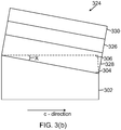
- the device structure 300 is grown on a top surface 304 of the GaN substrate 302, wherein the top surface 304 is oriented x degrees with respect to the m-plane 306 of the GaN substrate 300.
- the surface 304 may be a ⁇ 30-31 ⁇ plane or ⁇ 30-3-1 ⁇ plane.
- the device 300 is AlGaN cladding-free and the MOCVD growth conditions employed for growing the (30-31) the LD structure were similar to that typically used for c-plane, m-plane,
- the structure 300 comprises a thick lower GaN cladding layer 308 (e.g., n-type GaN layer on or above the semi-polar GaN crystal plane 304), a Si-doped InGaN waveguiding layer 310 (e.g., 50 nm thick n-type InGaN waveguiding layer 310 on or above the n-type GaN layer 308), an active layer on or above the n-type InGaN waveguiding layer 310, the active layer including three periods of an undoped InGaN quantum well (e.g., 5 nm thick) 312 sandwiched between GaN barriers 314a, 314b (e.g., 10 nm thick), an AlGaN electron blocking layer (EBL) 316, an Mg-doped InGaN upper waveguiding layer 318 (e.g., 50 nm thick p-type InGaN waveguiding layer on or above the quantum wells 312), an Mg-doped upper GaN cladding layer
- n-type GaN 308, n-type InGaN 310, active region 312, 314a, 314b, and p-type InGaN 318 were grown under N 2 ambient.
- the p-type GaN 320 was grown under H 2 ambient.
- the entire device was grown under high V/III ratio (>150). The structure and growth conditions are similar to those described in [7].
- the semi-polar crystal plane 304 and the depositing conditions may be such that one or more of the III-Nitride layers 308-322 have a surface roughness of 0.75 nm or less.
- FIG. 3(b) illustrates another embodiment of a device structure 324, grown during Block 202 on a semi-polar plane 304 of Block 200, wherein the device structure comprises one or more III-nitride or (Al,Ga,In)N active layers 326 (e.g., one or more InGaN quantum wells) between one or more n-type III-nitride or (Al,Ga,In)N layers 328 and one or more p-type III-nitride or (Al,Ga,In)N layers 330.
- III-nitride or (Al,Ga,In)N active layers 326 e.g., one or more InGaN quantum wells
- the n-type III-Nitride layers 328 may be on or above the semi-polar GaN crystal plane 304
- the III-Nitride active layer 326 may be on or above the n-type III-Nitride layers 328
- the p-type III-Nitride layers 330 may be on or above the III-Nitride active layers 326.
- the position of the n-type 328 and p-type 330 layers may be reversed. Also shown in FIG. 3(a) and FIG. 3(b) is the c-direction of the GaN substrate 302.
- the semi-polar crystal plane 304 may be a ⁇ 30-31 ⁇ , ⁇ 30-3-1 ⁇ , ⁇ 40-41 ⁇ , or ⁇ 40-4-1 ⁇ plane, for example.
- the semi-polar GaN crystal plane 304 provided in Block 200 may be a top surface of a vicinal, miscut, or off-axis free standing GaN substrate 302, for example, and the semi-polar GaN plane 304 may comprise an atomically specific plane, so that a smooth epitaxial growth of the III-Nitride layers (e.g., 308-322, 326, 328, 330) is achieved.
- one or more of the III-Nitride layers 308-322, 326, 328, 330 may have a surface roughness of 0.75 nm or less.
- the present invention is not limited to a particular thickness of the III-Nitride layers.
- the III-Nitride layers are not limited to a particular type of device layer, the III-Nitride active layers 326 are not limited to quantum wells or a particular type of active layer.
- the III-Nitride layers of the optoelectronic device may be device layers for a solar cell, photodetector, etc.
- the active layers 326 may be active layers for a solar cell, photodetector, etc.
- Block 204 represents processing the device (e.g., including forming mirror facets).
- Ridge-waveguide laser structures are fabricated using conventional photolithography, dry-etching, and lift-off techniques.
- the laser device structure of Block 202 was processed into a 10 ⁇ m by 1800 ⁇ m ridge waveguide LD using conventional photolithographic and dry etching techniques.
- a self-aligned dry etch and lift-off process was used to define the ridge waveguide and oxide insulator, and followed by 50/1000 nm Pd/Au metallization for the p-contact.
- Mirror facets were formed orthogonal to the in-plane projection of the c-axis by standard Cl 2 based reactive ion etching.
- Backside Al/Au n-contacts were deposited directly onto the bulk substrate.
- Block 206 represents the end result of the method, a device or optoelectronic device such as a laser diode or LED, grown on a semi-polar plane 304 or a semi-polar GaN crystal plane 304 (e.g., on a miscut GaN substrate 302), wherein the semi-polar plane 304 or semipolar GaN crystal plane 304 is miscut or oriented x degrees from an m-plane 306 of the GaN and in a c-direction of the GaN, where -15 ⁇ x ⁇ -1 and 1 ⁇ x ⁇ 15 degrees.
- a device or optoelectronic device such as a laser diode or LED
- an optoelectronic device may be grown on a miscut of GaN, wherein the miscut includes the semi-polar GaN crystal plane 304 miscut x degrees from an m-plane 306 of the GaN and in a c-direction of the GaN, where -15 ⁇ x ⁇ -1 and 1 ⁇ x ⁇ 15 degrees.
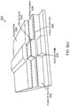
- FIG. 3(c) is a cross-sectional schematic of a finished laser device structure 332 of Block 206 with etched facets 334 (e.g., etched facet mirrors), ridge insulator 336, and p-contact pad 338.
- the LD may be on ⁇ 30-31 ⁇ , for example.
- the optoelectronic device may be an AlGaN cladding layer free LD comprising an InGaN waveguide that is thick enough to provide modal confinement.
- the morphological and structural qualities of the LD structure were characterized by repeating the identical growth conditions on separate (30-31) GaN substrates. Inconsistencies between separate MOCVD growths were shown to be minimal via photoluminescence measurements.
- FIG. 4 (a) shows a TEM image of the structure of FIG. 3(a) grown on a (30-31) semipolar crystal plane 304, showing high quality interfaces with no apparent defects.
- FIG. 4(a) shows n-type GaN layer 308 (n-GaN), n-type InGaN layer 310 (n-InGaN), InGaN quantum wells 312 with GaN barriers 314a, 314b (InGaN/GaN), p-type AlGaN EBL (p-AlGaN), p-type InGaN layer 318 (p-InGaN), and p-type layer 320 (p-GaN).
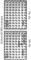
- FIG. 4(b) and FIG. 4(c) show Nomarski images of the (30-31) top surface 340 (opposite or parallel to surface 304) of n-type GaN layer 308 in the device structure of FIG. 3(a) , with obvious striations running along the [11-22] direction, which the present invention attributes to unoptimized growth conditions.
- FIG. 4(d)-FIG. 4(g) show how surface morphology may be optimized by growth conditions.
- FIG. 4(d) and FIG. 4(e) are Nomarski images of the top surface 340 of n-type GaN layer 308 in the device structure of FIG. 3(a) , grown by MOCVD on a (30-31) semipolar crystal plane 304 using N 2 ambient ( FIG. 4(d) ) and H 2 ambient ( FIG. 4(e) ).
- FIG. 4(f) and FIG. 4(g) are Nomarski images of the top surface 340 of n-type GaN layer 308 in FIG. 3(a) grown by MOCVD on a (30-3-1) semipolar crystal plane 304 using N 2 ambient ( FIG. 4(f) ) and H 2 ambient ( FIG. 4(g) ).
- RMS root mean square
- the 50 nm thick InGaN layer 310 was grown under N 2 ambient on the GaN 308 and the GaN 308 was grown under N 2 ambient at high temperature (e.g., approximately 900°C).
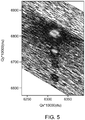
- FIG. 5 shows the x-ray reciprocal space mapping (RSM) of the LD structure 300 of FIG. 3(a) around the asymmetrical (20-25) diffraction of the (30-31) plane.
- RSM x-ray reciprocal space mapping
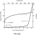
- FIG. 6(a) shows L-I-V characteristics
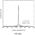
- FIG. 6(b) shows a lasing spectrum, of an etched facet LD having the structure of FIG. 3(a) grown on a ⁇ 30-3-1 ⁇ GaN substrate (and processed according to FIG. 2 ), showing an FWHM of 0.4 nm and a lasing peak at 477.5 nm.
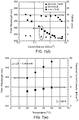
- FIGs. 7(a)-7(e) are measurements of the etched facet AlGaN cladding-free InGaN/GaN LD of FIG. 3(a) grown on a semipolar (30-31) GaN substrate and processed according to the steps of FIG. 2 .
- FIG. 7(a) shows L-I-V characteristics
- FIG. 7(b) shows the lasing spectrum of the etched facet AlGaN cladding-free InGaN/GaN LD. All measurements were taken at 20 °C using 1 ⁇ s pulses and a duty cycle of 0.1% to ensure minimal device self-heating effects.
- the lasing spectrum in FIG. 7(b) shows a clear lasing peak at 444.7 nm.
- the estimated threshold current ( I th ) was 1022 mA, which corresponds to a J th of 5.6 kA/cm 2 .
- the present invention attributes the relatively high threshold voltage of 9.9 V to unoptimized p-contacts and doping profiles.
- FIG. 7(c) shows a series of EL spectra measured as a function of current.
- FIG. 7(d) shows the peak EL wavelength shifted from approximately 448 nm at 0.03 kA/cm 2 to 444 nm just above threshold at 6.0 kA/cm 2 .
- This value of the EL blue-shift is comparable to m-plane LDs and considerably lower than c-plane LDs emitting at a similar wavelength (c-plane data is shown for comparison) [22, 8].
- FIG. 7(d) also shows the dependence of spectral width, or laser peak FWHM, on current density, which narrowed from 16.3 nm at 0.03 kA/cm 2 to 2.5 nm just above threshold.
- FIG. 7(e) shows J th and peak wavelength (at an output power of ⁇ 35 mW) as a function of stage temperature.
- a characteristic temperature (T o ) value of ⁇ 135 K was estimated by plotting the natural log of threshold current with respect to temperature and calculating the inverse of the slope. This value compares well to those reported for c-plane devices emitting at the same wavelength range [23-24].
- the dependence of the peak wavelength on temperature was calculated to be ⁇ 0.06 nm/K, which also corresponds well to values reported for LDs grown on m-plane, c-plane, and the (20-21) plane [9, 2, 25, 15].
- the present invention estimates a confinement factor of ⁇ 4.9% for the LD structure of FIG. 3(a) .
- a lasing with a lower confinement factor may be possible, and the LD structure of FIG. 3(a) may also have a higher confinement factor.
- the present invention enables improved laser performance.
- Higher critical thickness of strained (Al, Ga, In)N alloy layers epitaxially grown on semi-polar GaN substrates enable the present invention to improve modal confinement for coherent laser diode waveguide layers.
- Thicker quantum-wells help reduce effective carrier density in quantum-wells (reducing Auger-type losses) and can facilitate low transparency carrier density.
- Variations include various possible epitaxial growth techniques, laser device structures, different dry-etching techniques, including Inductively Coupled Plasma (ICP), Reactive Ion Etching (RIE), Focused Ion Beam (FIB), CMP, Chemically Assisted Ion Beam Etching (CAIBE), formation of facet mirrors by cleaving, formation of facet mirrors by laser ablation, variations in waveguide structures, facets made by two types of etching techniques or different angles (superluminescent diodes (SLDs)), and facets mirrors coated with the same/two different types of dielectrics, etc.
- ICP Inductively Coupled Plasma
- RIE Reactive Ion Etching
- FIB Focused Ion Beam
- CMP Chemically Assisted Ion Beam Etching
- facet mirrors by cleaving formation of facet mirrors by laser ablation
- variations in waveguide structures facets made by two types of etching techniques or different angles (superluminescent diodes (SLDs)), and facets mirror
- the semi-polar crystal plane 304 may be a semi-polar GaN crystal plane or a semi-polar III-Nitride crystal plane.
- the semi-polar crystal plane may be a semi-polar plane 304 of GaN (e.g., GaN substrate) or of a III-Nitride (e.g., III-Nitride substrate).
- the semi-polar plane 304 of the present invention is oriented or miscut x degrees from an m-plane of GaN in a c-direction of the III-Nitride, where -15 ⁇ x ⁇ -1 or 1 ⁇ x ⁇ 15.
- the semi-polar plane 304 may be planar.
- One or more of the III-Nitride layers 308-322 may be planar layers.
- one or more of the III-Nitride layers 308-322, 326, 328, 330 may have a top surface (e.g. 340, 342) that is planar.
- One or more of the III-Nitride layers 308-322, 326, 328, 330 may have interfaces (with other III-Nitride layers) that are planar.
- Variations also include other optoelectronic devices (LEDs, photonic crystal lasers, solar cells, photodetectors, etc.) grown on m-plane substrates miscut x degrees in the c-direction (where -15 ⁇ x ⁇ -1 or 1 ⁇ x ⁇ 15).
- LEDs light-emitting diode
- SLDs semiconductor lasers
- VCSEL lasers VCSEL lasers
- the critical thickness of strained epitaxial (Al, Ga, In)N alloy layers on such GaN miscut m-plane substrates may also be larger than other semi-polar (i.e., ⁇ 11-22 ⁇ , ⁇ 10-1-1 ⁇ , and ⁇ 20-21 ⁇ ) crystal planes with miscuts larger than +/-15 degrees from the m-plane in the c-direction. This enables higher thickness and composition for waveguide layers - thus improving modal gain.
- the present invention's working prototype laser devices on the ⁇ 30-31 ⁇ and ⁇ 30-3-1 ⁇ plane demonstrates the potential of devices on such m-plane miscut substrates.
- Applications for the devices of the present invention include, but are not limited to, optoelectronic devices (lasers, LEDs, etc) for display, lighting, biomedical imaging, illumination applications, etc.
Claims (15)
- Dispositif optoélectronique (300), comprenant :
une ou plusieurs couches de nitrure III semi-polaires (308-322) formées par croissance épitaxiale sur un plan cristallin semi-polaire (304) d'un substrat en GaN (302), dans lequel :le plan cristallin semi-polaire (304) est orienté à x degrés d'un plan m (306) de GaN dans une direction c de GaN, avec -15 < x < -1 ou 1 < x < 15 ; etles couches de nitrure III (308-322) comprennent une couche d'(Al,In,Ga)N ayant une épaisseur supérieure ou égale à une épaisseur critique de Matthews-Blakeslee pour une telle couche déposée sur un plan cristallin semi-polaire de GaN orienté à 15 degrés ou plus d'un plan m de GaN dans une direction c de GaN. - Dispositif selon la revendication 1, dans lequel :le plan cristallin semi-polaire (304) orienté à x degrés d'un plan m (306) de GaN dans une direction c de GaN est un plan {30-31}, {30-3-1}, {40-41} ou {40-4-1}, etle plan cristallin semi-polaire de GaN orienté à 15 degrés ou plus d'un plan m de GaN dans la direction c de GaN est un plan {11-22}, {10-1-1} ou {20-21}.
- Dispositif selon la revendication 1, dans lequel la couche d'(Al,In,Ga)N est une couche d'InGaN.
- Dispositif selon la revendication 3, dans lequel :le dispositif optoélectronique (300) est une diode laser et les couches de nitrure III semi-polaires (308-322) comprennent une ou plusieurs couches d'InGaN comprenant un guide d'ondes d'InGaN (310, 318) qui fournit un confinement modal pour la diode laser ; etles couches de nitrure III semi-polaires comprennent en outre une couche active d'InGaN électroluminescente comprenant un ou plusieurs puits quantiques d'InGaN (312), un ou plusieurs des puits quantiques ayant une composition d'indium d'au moins 16 % et une épaisseur d'au moins 4 nanomètres.
- Dispositif selon la revendication 1 ou 3, dans lequel les couches de nitrure III semi-polaires (308-322) comprennent une ou plusieurs couches d'InGaN ayant une composition d'indium d'au moins 7 %, et le plan cristallin semi-polaire (304) est une surface supérieure d'un substrat en GaN autonome vicinal, mal coupé ou hors axe (302).
- Dispositif selon la revendication 1, dans lequel le dispositif optoélectronique (300) est formé par croissance sur une surface mal coupée ou vicinale d'un substrat en GaN (302), la surface mal coupée ou vicinale comprenant le plan cristallin semi-polaire (304), et les couches de nitrure III (308-322) comprenant en outre :une ou plusieurs couches de nitrure III ou d'(Al,In,Ga)N de type n (308, 310) ;une ou plusieurs couches de nitrure III ou d'(Al,In,Ga)N de type p (318, 320, 322) ; etune couche active d'InGaN comprenant une ou plusieurs couches de puits quantiques d'InGaN (312) entre les couches de nitrure III ou d'(Al,In,Ga)N de type n (308, 310) et la ou les couches d'(Al,In,Ga)N de type p (318, 320, 322), les couches de nitrure III ou d'(Al,In,Ga)N de type n (308, 310), les couches de nitrure III ou d'(Al,In,Ga)N de type p (318, 320, 322), et les couches de puits quantiques d'InGaN (312) ayant une orientation semi-polaire du plan cristallin semi-polaire (304) et les couches de puits quantiques d'InGaN (312) ayant une émission de lumière maximale ou une absorption de lumière maximale à une longueur d'onde d'au moins 477 nm, oule dispositif optoélectronique (300) étant une diode laser, et les couches de nitrure III semi-polaires (308-322) comprenant :une couche de GaN de type n (308) sur ou au-dessus du plan cristallin semi-polaire (304) ;les couches de nitrure III semi-polaires (308-322) comprenant en outre une couche de guide d'ondes d'InGaN de type n (310) sur ou au-dessus de la couche de GaN de type n (308), la couche de guide d'ondes d'InGaN de type n (310) ayant une épaisseur d'au moins 50 nm et une composition d'indium de 7 % ou plus ;une couche active d'InGaN sur ou au-dessus de la couche de guide d'ondes d'InGaN de type n (310), comprenant une ou plusieurs couches de puits quantiques d'InGaN (312) ayant une composition d'indium d'au moins 7 % et une épaisseur d'au moins 4 nm ;les couches de nitrure III semi-polaires (308-322) comprenant en outre une couche de guide d'ondes d'InGaN de type p (318) sur ou au-dessus de la couche active d'InGaN ; etune couche de GaN de type p (320, 322) sur ou au-dessus de la couche de guide d'ondes d'InGaN de type p (318), la couche de guide d'ondes d'InGaN de type p (318) ayant une épaisseur d'au moins 50 nm et une composition d'indium de 7 % ou plus, les couches de nitrure III (308-322) ayant une orientation semi-polaire du plan cristallin semi-polaire (304).
- Dispositif selon la revendication 1, dans lequel une ou plusieurs des couches de nitrure III semi-polaires (308-322) ont une rugosité de surface de 0,75 nm ou moins.
- Dispositif selon la revendication 1, dans lequel :une ou plusieurs des couches de nitrure III semi-polaires (308-322) ont une ou plusieurs épaisseurs et une ou plusieurs compositions ; etle dispositif optoélectronique (300) est une diode laser, la ou les couches de nitrure III semi-polaires comprenant un guide d'ondes (310, 318) et une région active.
- Procédé de fabrication d'un dispositif optoélectronique, comprenant :le dépôt épitaxial (202) de couches de nitrure III semi-polaires sur un plan cristallin semi-polaire de GaN,le plan cristallin semi-polaire étant orienté à x degrés d'un plan m de GaN dans une direction c de GaN, avec -15 < x < -1 ou 1 < x < 15 ; etles couches de nitrure III comprenant une couche d'(Al,In,Ga)N ayant une épaisseur supérieure ou égale à une épaisseur critique de Matthews-Blakeslee pour une telle couche déposée sur un plan cristallin semi-polaire de GaN orienté à 15 degrés ou plus d'un plan m de GaN dans une direction c de GaN.
- Procédé selon la revendication 9, dans lequel la couche d'(Al,In,Ga)N est une couche d'InGaN, ou dans lequel les couches de nitrure III semi-polaires comprennent une ou plusieurs couches d'InGaN ayant une composition d'indium d'au moins 7 %, et le plan cristallin semi-polaire est une surface supérieure d'un substrat en GaN autonome vicinal, mal coupé ou hors axe.
- Procédé selon la revendication 10, dans lequel :le dispositif optoélectronique est une diode laser, et les couches de nitrure III comprennent une ou plusieurs couches d'InGaN comprenant un guide d'ondes d'InGaN qui fournit un confinement modal pour la diode laser, la diode laser ayant un maximum laser à une longueur d'onde d'au moins 460 nm ; etle dépôt (202) des couches de nitrure III comprend en outre le dépôt d'une couche active d'InGaN électroluminescente comprenant un ou plusieurs puits quantiques d'InGaN, un ou plusieurs des puits quantiques ayant une composition d'indium d'au moins 16 % et une épaisseur d'au moins 4 nanomètres.
- Procédé selon la revendication 9, dans lequel le dispositif optoélectronique est une diode laser, le dépôt (202) des couches de nitrure III semi-polaires comprenant en outre :le dépôt d'une couche de GaN de type n sur ou au-dessus du plan cristallin semi-polaire ;le dépôt d'une couche de guide d'ondes d'InGaN de type n sur ou au-dessus de la couche de GaN de type n, la couche de guide d'ondes d'InGaN de type n ayant une épaisseur d'au moins 50 nm et une composition d'indium de 7 % ou plus ;le dépôt d'une couche active d'InGaN sur ou au-dessus de la couche de guide d'ondes d'InGaN de type n, comprenant une ou plusieurs couches de puits quantiques d'InGaN ayant une composition d'indium d'au moins 7 % et une épaisseur d'au moins 4 nm;le dépôt d'une couche de guide d'ondes d'InGaN de type p sur ou au-dessus des puits quantiques d'InGaN ; etle dépôt d'une couche de GaN de type p sur ou au-dessus de la couche de guide d'ondes d'InGaN de type p, la couche de guide d'ondes d'InGaN de type p ayant une épaisseur d'au moins 50 nm et une composition d'indium de 7 % ou plus, les couches de nitrure III ayant une orientation semi-polaire du plan cristallin semi-polaire.
- Procédé selon la revendication 9, dans lequel :le plan cristallin semi-polaire orienté à x degrés d'un plan m de GaN dans une direction c de GaN est un plan {30-31}, {30-3-1}, {40-41} ou {40-4-1}, etle plan cristallin semi-polaire de GaN orienté à 15 degrés ou plus d'un plan m de GaN dans la direction c de GaN est un plan {11-22}, {10-1-1} ou {20-21}.
- Procédé selon la revendication 9, dans lequel le plan cristallin semi-polaire et les conditions de dépôt sont tels qu'une ou plusieurs des couches de nitrure III aient une rugosité de surface de 0,75 nm ou moins.
- Procédé selon la revendication 9, dans lequel :une ou plusieurs des couches de nitrure III semi-polaires ont une ou plusieurs épaisseurs et une ou plusieurs compositions ; etle dispositif optoélectronique est une diode laser, la ou les couches de nitrure III semi-polaires comprenant un guide d'ondes et une région active.
Applications Claiming Priority (2)
| Application Number | Priority Date | Filing Date | Title |
|---|---|---|---|
| US31063810P | 2010-03-04 | 2010-03-04 | |
| PCT/US2011/027267 WO2011109754A1 (fr) | 2010-03-04 | 2011-03-04 | Dispositifs optoélectroniques semi-polaires à base de nitrure de groupe iii sur des substrats de plan m avec « miscuts » inférieurs à +/-15 degrés dans la direction c |
Publications (3)
| Publication Number | Publication Date |
|---|---|
| EP2543119A1 EP2543119A1 (fr) | 2013-01-09 |
| EP2543119A4 EP2543119A4 (fr) | 2015-08-12 |
| EP2543119B1 true EP2543119B1 (fr) | 2020-02-12 |
Family
ID=44531316
Family Applications (1)
| Application Number | Title | Priority Date | Filing Date |
|---|---|---|---|
| EP11751456.2A Active EP2543119B1 (fr) | 2010-03-04 | 2011-03-04 | Dispositifs optoélectroniques semi-polaires à base de nitrure de groupe iii sur des substrats de gan de plan m à angle de coupe entre 1 et 15 degrés ou entre -1 et -15 degrés dans la direction c |
Country Status (7)
| Country | Link |
|---|---|
| US (3) | US9077151B2 (fr) |
| EP (1) | EP2543119B1 (fr) |
| JP (3) | JP5972798B2 (fr) |
| KR (1) | KR101854419B1 (fr) |
| CN (2) | CN106972346B (fr) |
| TW (1) | TWI560963B (fr) |
| WO (1) | WO2011109754A1 (fr) |
Families Citing this family (96)
| Publication number | Priority date | Publication date | Assignee | Title |
|---|---|---|---|---|
| US8847249B2 (en) | 2008-06-16 | 2014-09-30 | Soraa, Inc. | Solid-state optical device having enhanced indium content in active regions |
| US8143148B1 (en) | 2008-07-14 | 2012-03-27 | Soraa, Inc. | Self-aligned multi-dielectric-layer lift off process for laser diode stripes |
| US8767787B1 (en) | 2008-07-14 | 2014-07-01 | Soraa Laser Diode, Inc. | Integrated laser diodes with quality facets on GaN substrates |
| US8805134B1 (en) | 2012-02-17 | 2014-08-12 | Soraa Laser Diode, Inc. | Methods and apparatus for photonic integration in non-polar and semi-polar oriented wave-guided optical devices |
| CN102144294A (zh) | 2008-08-04 | 2011-08-03 | Soraa有限公司 | 使用非极性或半极性的含镓材料和磷光体的白光器件 |
| US8284810B1 (en) | 2008-08-04 | 2012-10-09 | Soraa, Inc. | Solid state laser device using a selected crystal orientation in non-polar or semi-polar GaN containing materials and methods |
| US8247886B1 (en) | 2009-03-09 | 2012-08-21 | Soraa, Inc. | Polarization direction of optical devices using selected spatial configurations |
| US8422525B1 (en) | 2009-03-28 | 2013-04-16 | Soraa, Inc. | Optical device structure using miscut GaN substrates for laser applications |
| US8634442B1 (en) | 2009-04-13 | 2014-01-21 | Soraa Laser Diode, Inc. | Optical device structure using GaN substrates for laser applications |
| US9531164B2 (en) | 2009-04-13 | 2016-12-27 | Soraa Laser Diode, Inc. | Optical device structure using GaN substrates for laser applications |
| US8837545B2 (en) | 2009-04-13 | 2014-09-16 | Soraa Laser Diode, Inc. | Optical device structure using GaN substrates and growth structures for laser applications |
| US8791499B1 (en) | 2009-05-27 | 2014-07-29 | Soraa, Inc. | GaN containing optical devices and method with ESD stability |
| US8427590B2 (en) | 2009-05-29 | 2013-04-23 | Soraa, Inc. | Laser based display method and system |
| US8247887B1 (en) | 2009-05-29 | 2012-08-21 | Soraa, Inc. | Method and surface morphology of non-polar gallium nitride containing substrates |
| US9250044B1 (en) | 2009-05-29 | 2016-02-02 | Soraa Laser Diode, Inc. | Gallium and nitrogen containing laser diode dazzling devices and methods of use |
| US8509275B1 (en) | 2009-05-29 | 2013-08-13 | Soraa, Inc. | Gallium nitride based laser dazzling device and method |
| US9800017B1 (en) | 2009-05-29 | 2017-10-24 | Soraa Laser Diode, Inc. | Laser device and method for a vehicle |
| US9829780B2 (en) | 2009-05-29 | 2017-11-28 | Soraa Laser Diode, Inc. | Laser light source for a vehicle |
| US10108079B2 (en) | 2009-05-29 | 2018-10-23 | Soraa Laser Diode, Inc. | Laser light source for a vehicle |
| JP5206699B2 (ja) | 2010-01-18 | 2013-06-12 | 住友電気工業株式会社 | Iii族窒化物半導体レーザ素子、及びiii族窒化物半導体レーザ素子を作製する方法 |
| US7933303B2 (en) * | 2009-06-17 | 2011-04-26 | Sumitomo Electric Industries, Ltd. | Group-III nitride semiconductor laser device, and method for fabricating group-III nitride semiconductor laser device |
| JP5234022B2 (ja) * | 2009-07-15 | 2013-07-10 | 住友電気工業株式会社 | 窒化物系半導体発光素子 |
| US9000466B1 (en) | 2010-08-23 | 2015-04-07 | Soraa, Inc. | Methods and devices for light extraction from a group III-nitride volumetric LED using surface and sidewall roughening |
| US8750342B1 (en) | 2011-09-09 | 2014-06-10 | Soraa Laser Diode, Inc. | Laser diodes with scribe structures |
| US8355418B2 (en) | 2009-09-17 | 2013-01-15 | Soraa, Inc. | Growth structures and method for forming laser diodes on {20-21} or off cut gallium and nitrogen containing substrates |
| US8933644B2 (en) | 2009-09-18 | 2015-01-13 | Soraa, Inc. | LED lamps with improved quality of light |
| US9583678B2 (en) | 2009-09-18 | 2017-02-28 | Soraa, Inc. | High-performance LED fabrication |
| US9293644B2 (en) | 2009-09-18 | 2016-03-22 | Soraa, Inc. | Power light emitting diode and method with uniform current density operation |
| US8905588B2 (en) | 2010-02-03 | 2014-12-09 | Sorra, Inc. | System and method for providing color light sources in proximity to predetermined wavelength conversion structures |
| US10147850B1 (en) | 2010-02-03 | 2018-12-04 | Soraa, Inc. | System and method for providing color light sources in proximity to predetermined wavelength conversion structures |
| WO2011109754A1 (fr) | 2010-03-04 | 2011-09-09 | The Regents Of The University Of California | Dispositifs optoélectroniques semi-polaires à base de nitrure de groupe iii sur des substrats de plan m avec « miscuts » inférieurs à +/-15 degrés dans la direction c |
| US9927611B2 (en) | 2010-03-29 | 2018-03-27 | Soraa Laser Diode, Inc. | Wearable laser based display method and system |
| US8451876B1 (en) | 2010-05-17 | 2013-05-28 | Soraa, Inc. | Method and system for providing bidirectional light sources with broad spectrum |
| US8189639B2 (en) * | 2010-05-28 | 2012-05-29 | Corning Incorporated | GaN-based laser diodes with misfit dislocations displaced from the active region |
| US9450143B2 (en) | 2010-06-18 | 2016-09-20 | Soraa, Inc. | Gallium and nitrogen containing triangular or diamond-shaped configuration for optical devices |
| US8816319B1 (en) | 2010-11-05 | 2014-08-26 | Soraa Laser Diode, Inc. | Method of strain engineering and related optical device using a gallium and nitrogen containing active region |
| US9048170B2 (en) | 2010-11-09 | 2015-06-02 | Soraa Laser Diode, Inc. | Method of fabricating optical devices using laser treatment |
| US9595813B2 (en) | 2011-01-24 | 2017-03-14 | Soraa Laser Diode, Inc. | Laser package having multiple emitters configured on a substrate member |
| US8786053B2 (en) | 2011-01-24 | 2014-07-22 | Soraa, Inc. | Gallium-nitride-on-handle substrate materials and devices and method of manufacture |
| US9025635B2 (en) | 2011-01-24 | 2015-05-05 | Soraa Laser Diode, Inc. | Laser package having multiple emitters configured on a support member |
| US9318875B1 (en) | 2011-01-24 | 2016-04-19 | Soraa Laser Diode, Inc. | Color converting element for laser diode |
| US9093820B1 (en) | 2011-01-25 | 2015-07-28 | Soraa Laser Diode, Inc. | Method and structure for laser devices using optical blocking regions |
| US9236530B2 (en) * | 2011-04-01 | 2016-01-12 | Soraa, Inc. | Miscut bulk substrates |
| US9287684B2 (en) | 2011-04-04 | 2016-03-15 | Soraa Laser Diode, Inc. | Laser package having multiple emitters with color wheel |
| US8686431B2 (en) | 2011-08-22 | 2014-04-01 | Soraa, Inc. | Gallium and nitrogen containing trilateral configuration for optical devices |
| US9646827B1 (en) | 2011-08-23 | 2017-05-09 | Soraa, Inc. | Method for smoothing surface of a substrate containing gallium and nitrogen |
| US8971370B1 (en) | 2011-10-13 | 2015-03-03 | Soraa Laser Diode, Inc. | Laser devices using a semipolar plane |
| US8912025B2 (en) | 2011-11-23 | 2014-12-16 | Soraa, Inc. | Method for manufacture of bright GaN LEDs using a selective removal process |
| WO2013134432A1 (fr) | 2012-03-06 | 2013-09-12 | Soraa, Inc. | Diodes électroluminescentes à couches de matériau à faible indice de réfraction destinées à réduire des effets de guidage de lumière |
| US9020003B1 (en) | 2012-03-14 | 2015-04-28 | Soraa Laser Diode, Inc. | Group III-nitride laser diode grown on a semi-polar orientation of gallium and nitrogen containing substrates |
| EP2832901A4 (fr) | 2012-03-30 | 2015-07-08 | Mitsubishi Chem Corp | Cristaux de nitrure de métal de groupe 13 du tableau périodique des éléments et procédé de fabrication de cristaux de nitrure de métal de groupe 13 du tableau périodique des éléments |
| US9343871B1 (en) | 2012-04-05 | 2016-05-17 | Soraa Laser Diode, Inc. | Facet on a gallium and nitrogen containing laser diode |
| US20130322481A1 (en) * | 2012-05-31 | 2013-12-05 | Rajaram Bhat | Laser diodes including substrates having semipolar surface plane orientations and nonpolar cleaved facets |
| US9099843B1 (en) | 2012-07-19 | 2015-08-04 | Soraa Laser Diode, Inc. | High operating temperature laser diodes |
| US8971368B1 (en) | 2012-08-16 | 2015-03-03 | Soraa Laser Diode, Inc. | Laser devices having a gallium and nitrogen containing semipolar surface orientation |
| US9978904B2 (en) | 2012-10-16 | 2018-05-22 | Soraa, Inc. | Indium gallium nitride light emitting devices |
| US20140126599A1 (en) * | 2012-11-06 | 2014-05-08 | The Regents Of The University Of California | (Al,In,B,Ga)N BASED SEMIPOLAR AND NONPOLAR LASER DIODES WITH POLISHED FACETS |
| US8802471B1 (en) | 2012-12-21 | 2014-08-12 | Soraa, Inc. | Contacts for an n-type gallium and nitrogen substrate for optical devices |
| US9166372B1 (en) | 2013-06-28 | 2015-10-20 | Soraa Laser Diode, Inc. | Gallium nitride containing laser device configured on a patterned substrate |
| US8994033B2 (en) | 2013-07-09 | 2015-03-31 | Soraa, Inc. | Contacts for an n-type gallium and nitrogen substrate for optical devices |
| US9685577B2 (en) * | 2013-10-15 | 2017-06-20 | The Penn State Research Foundation | Light emitting diodes and photodetectors |
| US9379525B2 (en) | 2014-02-10 | 2016-06-28 | Soraa Laser Diode, Inc. | Manufacturable laser diode |
| US9368939B2 (en) | 2013-10-18 | 2016-06-14 | Soraa Laser Diode, Inc. | Manufacturable laser diode formed on C-plane gallium and nitrogen material |
| US9520695B2 (en) | 2013-10-18 | 2016-12-13 | Soraa Laser Diode, Inc. | Gallium and nitrogen containing laser device having confinement region |
| US9362715B2 (en) | 2014-02-10 | 2016-06-07 | Soraa Laser Diode, Inc | Method for manufacturing gallium and nitrogen bearing laser devices with improved usage of substrate material |
| US9368582B2 (en) * | 2013-11-04 | 2016-06-14 | Avogy, Inc. | High power gallium nitride electronics using miscut substrates |
| US9419189B1 (en) | 2013-11-04 | 2016-08-16 | Soraa, Inc. | Small LED source with high brightness and high efficiency |
| WO2015089379A1 (fr) * | 2013-12-13 | 2015-06-18 | The Regents Of The University Of California | Diodes électroluminescentes semi-polaires {30-3-1} à haute puissance à faible chute de courant et faible chute thermique |
| US9209596B1 (en) | 2014-02-07 | 2015-12-08 | Soraa Laser Diode, Inc. | Manufacturing a laser diode device from a plurality of gallium and nitrogen containing substrates |
| US9520697B2 (en) | 2014-02-10 | 2016-12-13 | Soraa Laser Diode, Inc. | Manufacturable multi-emitter laser diode |
| US9871350B2 (en) | 2014-02-10 | 2018-01-16 | Soraa Laser Diode, Inc. | Manufacturable RGB laser diode source |
| US9564736B1 (en) | 2014-06-26 | 2017-02-07 | Soraa Laser Diode, Inc. | Epitaxial growth of p-type cladding regions using nitrogen gas for a gallium and nitrogen containing laser diode |
| US9246311B1 (en) | 2014-11-06 | 2016-01-26 | Soraa Laser Diode, Inc. | Method of manufacture for an ultraviolet laser diode |
| US9653642B1 (en) | 2014-12-23 | 2017-05-16 | Soraa Laser Diode, Inc. | Manufacturable RGB display based on thin film gallium and nitrogen containing light emitting diodes |
| US9666677B1 (en) | 2014-12-23 | 2017-05-30 | Soraa Laser Diode, Inc. | Manufacturable thin film gallium and nitrogen containing devices |
| US10938182B2 (en) | 2015-08-19 | 2021-03-02 | Soraa Laser Diode, Inc. | Specialized integrated light source using a laser diode |
| US11437774B2 (en) | 2015-08-19 | 2022-09-06 | Kyocera Sld Laser, Inc. | High-luminous flux laser-based white light source |
| US11437775B2 (en) | 2015-08-19 | 2022-09-06 | Kyocera Sld Laser, Inc. | Integrated light source using a laser diode |
| US10879673B2 (en) | 2015-08-19 | 2020-12-29 | Soraa Laser Diode, Inc. | Integrated white light source using a laser diode and a phosphor in a surface mount device package |
| US9787963B2 (en) | 2015-10-08 | 2017-10-10 | Soraa Laser Diode, Inc. | Laser lighting having selective resolution |
| JP6885547B2 (ja) | 2016-03-15 | 2021-06-16 | 三菱ケミカル株式会社 | GaN結晶の製造方法 |
| CN109476501B (zh) | 2016-06-29 | 2021-11-09 | 住友大阪水泥股份有限公司 | 氧化钛粒子、以及使用其的氧化钛粒子分散液及化妆料 |
| US10771155B2 (en) | 2017-09-28 | 2020-09-08 | Soraa Laser Diode, Inc. | Intelligent visible light with a gallium and nitrogen containing laser source |
| US10222474B1 (en) | 2017-12-13 | 2019-03-05 | Soraa Laser Diode, Inc. | Lidar systems including a gallium and nitrogen containing laser light source |
| CN108389942A (zh) * | 2018-02-07 | 2018-08-10 | 赛富乐斯股份有限公司 | 发光装置及其制造方法 |
| US10551728B1 (en) | 2018-04-10 | 2020-02-04 | Soraa Laser Diode, Inc. | Structured phosphors for dynamic lighting |
| US11402672B2 (en) * | 2018-05-03 | 2022-08-02 | X Development Llc | Quantum confined nanostructures with improved homogeneity and methods for making the same |
| US11239637B2 (en) | 2018-12-21 | 2022-02-01 | Kyocera Sld Laser, Inc. | Fiber delivered laser induced white light system |
| US11421843B2 (en) | 2018-12-21 | 2022-08-23 | Kyocera Sld Laser, Inc. | Fiber-delivered laser-induced dynamic light system |
| US11884202B2 (en) | 2019-01-18 | 2024-01-30 | Kyocera Sld Laser, Inc. | Laser-based fiber-coupled white light system |
| GB2580956B (en) * | 2019-01-31 | 2023-01-25 | Exalos Ag | Amplified Spontaneous Emission Semiconductor Source |
| US11228158B2 (en) | 2019-05-14 | 2022-01-18 | Kyocera Sld Laser, Inc. | Manufacturable laser diodes on a large area gallium and nitrogen containing substrate |
| US10903623B2 (en) | 2019-05-14 | 2021-01-26 | Soraa Laser Diode, Inc. | Method and structure for manufacturable large area gallium and nitrogen containing substrate |
| US11195973B1 (en) * | 2019-05-17 | 2021-12-07 | Facebook Technologies, Llc | III-nitride micro-LEDs on semi-polar oriented GaN |
| US11175447B1 (en) | 2019-08-13 | 2021-11-16 | Facebook Technologies, Llc | Waveguide in-coupling using polarized light emitting diodes |
| EP4083670A1 (fr) | 2021-04-30 | 2022-11-02 | Nokia Solutions and Networks Oy | Circuits de guides d'ondes optiques ayant des noyaux de guides d'ondes inclinés latéralement |
Family Cites Families (58)
| Publication number | Priority date | Publication date | Assignee | Title |
|---|---|---|---|---|
| US3011708A (en) | 1956-10-19 | 1961-12-05 | Howard A Reed | Reset unit for voting machines |
| US6849472B2 (en) | 1997-09-30 | 2005-02-01 | Lumileds Lighting U.S., Llc | Nitride semiconductor device with reduced polarization fields |
| US6163557A (en) * | 1998-05-21 | 2000-12-19 | Xerox Corporation | Fabrication of group III-V nitrides on mesas |
| TW480751B (en) * | 2001-04-09 | 2002-03-21 | Uni Light Technology Inc | Semiconductor light emitting diode based on off-cut substrate |
| US6833564B2 (en) | 2001-11-02 | 2004-12-21 | Lumileds Lighting U.S., Llc | Indium gallium nitride separate confinement heterostructure light emitting devices |
| US6683327B2 (en) | 2001-11-13 | 2004-01-27 | Lumileds Lighting U.S., Llc | Nucleation layer for improved light extraction from light emitting devices |
| JP3951013B2 (ja) * | 2002-05-07 | 2007-08-01 | 独立行政法人産業技術総合研究所 | 固体ターゲットパルスレーザ蒸着法によるGaN結晶性薄膜の作製方法及び同法で作製した薄膜 |
| US7122734B2 (en) | 2002-10-23 | 2006-10-17 | The Boeing Company | Isoelectronic surfactant suppression of threading dislocations in metamorphic epitaxial layers |
| US7118813B2 (en) | 2003-11-14 | 2006-10-10 | Cree, Inc. | Vicinal gallium nitride substrate for high quality homoepitaxy |
| JP3816942B2 (ja) | 2004-10-27 | 2006-08-30 | 三菱電機株式会社 | 半導体素子の製造方法 |
| JP2006332370A (ja) | 2005-05-26 | 2006-12-07 | Sumitomo Electric Ind Ltd | 窒化物半導体発光素子 |
| US8148713B2 (en) * | 2008-04-04 | 2012-04-03 | The Regents Of The University Of California | Method for fabrication of semipolar (Al, In, Ga, B)N based light emitting diodes |
| JP5048236B2 (ja) * | 2005-11-10 | 2012-10-17 | 住友電気工業株式会社 | 半導体発光素子、および半導体発光素子を作製する方法 |
| TWI490918B (zh) * | 2006-01-20 | 2015-07-01 | Univ California | 半極性氮化(鋁,銦,鎵,硼)之改良成長方法 |
| CN101009346A (zh) * | 2006-01-27 | 2007-08-01 | 中国科学院物理研究所 | 硅衬底上生长的非极性a面氮化物薄膜及其制法和用途 |
| KR100837404B1 (ko) | 2006-10-18 | 2008-06-12 | 삼성전자주식회사 | 반도체 광전 소자 |
| JP5332168B2 (ja) | 2006-11-17 | 2013-11-06 | 住友電気工業株式会社 | Iii族窒化物結晶の製造方法 |
| JP2010512660A (ja) * | 2006-12-11 | 2010-04-22 | ザ リージェンツ オブ ザ ユニバーシティ オブ カリフォルニア | 無極性および半極性の発光デバイス |
| CN101652832B (zh) * | 2007-01-26 | 2011-06-22 | 晶体公司 | 厚的赝晶氮化物外延层 |
| JP2008285364A (ja) | 2007-05-17 | 2008-11-27 | Sumitomo Electric Ind Ltd | GaN基板、それを用いたエピタキシャル基板及び半導体発光素子 |
| WO2008157510A1 (fr) | 2007-06-15 | 2008-12-24 | The Regents Of The University Of California | Films en nitrure du groupe iii à plan m non polaires plans mis à croître sur des substrats de mauvaise coupe |
| KR101537300B1 (ko) | 2007-08-08 | 2015-07-16 | 더 리전츠 오브 더 유니버시티 오브 캘리포니아 | 미스컷 기판들 상에 성장된 평면의 무극성 m-면 Ⅲ족-질화물 막들 |
| JP2010539732A (ja) * | 2007-09-19 | 2010-12-16 | ザ リージェンツ オブ ザ ユニバーシティ オブ カリフォルニア | 無極性および半極性の窒化物基板の面積を増加させる方法 |
| TW201442280A (zh) * | 2007-11-30 | 2014-11-01 | Univ California | 利用表面粗糙之高度光取出效率之氮化物基發光二極體 |
| JP2009152276A (ja) | 2007-12-19 | 2009-07-09 | Mitsubishi Electric Corp | 窒化物半導体レーザの製造方法 |
| KR20100107054A (ko) * | 2008-02-01 | 2010-10-04 | 더 리전츠 오브 더 유니버시티 오브 캘리포니아 | 웨이퍼 비축 절단에 의한 질화물 발광 다이오드들의 광학 편광의 강화 |
| KR20100129280A (ko) | 2008-02-01 | 2010-12-08 | 더 리전츠 오브 더 유니버시티 오브 캘리포니아 | 증가된 인듐 도입에 의한 질화물 발광 다이오드들의 광학 편광의 강화 |
| JP2009252861A (ja) * | 2008-04-03 | 2009-10-29 | Rohm Co Ltd | 半導体レーザ素子 |
| TW200950162A (en) * | 2008-04-04 | 2009-12-01 | Univ California | Method for fabrication of semipolar (Al, In, Ga, B)N based light emitting diodes |
| EP2281076A1 (fr) * | 2008-06-04 | 2011-02-09 | Sixpoint Materials, Inc. | Procédés de création des cristaux de nitrure du groupe iii de cristallinité améliorée à partir de germe de nitrure du groupe iii initial par croissance ammoniothermique |
| JP5295871B2 (ja) * | 2008-07-03 | 2013-09-18 | 古河機械金属株式会社 | Iii族窒化物半導体基板の製造方法 |
| JP4572963B2 (ja) | 2008-07-09 | 2010-11-04 | 住友電気工業株式会社 | Iii族窒化物系半導体発光素子、及びエピタキシャルウエハ |
| JP4475358B1 (ja) | 2008-08-04 | 2010-06-09 | 住友電気工業株式会社 | GaN系半導体光素子、GaN系半導体光素子を作製する方法、及びエピタキシャルウエハ |
| US8284810B1 (en) * | 2008-08-04 | 2012-10-09 | Soraa, Inc. | Solid state laser device using a selected crystal orientation in non-polar or semi-polar GaN containing materials and methods |
| JP5077303B2 (ja) * | 2008-10-07 | 2012-11-21 | 住友電気工業株式会社 | 窒化ガリウム系半導体発光素子、窒化ガリウム系半導体発光素子を作製する方法、窒化ガリウム系発光ダイオード、エピタキシャルウエハ、及び窒化ガリウム系発光ダイオードを作製する方法 |
| JP2010123920A (ja) * | 2008-10-20 | 2010-06-03 | Sumitomo Electric Ind Ltd | 窒化物系半導体発光素子を作製する方法、及びエピタキシャルウエハを作製する方法 |
| JP4775455B2 (ja) * | 2009-02-17 | 2011-09-21 | 住友電気工業株式会社 | Iii族窒化物半導体レーザ、及びiii族窒化物半導体レーザを作製する方法 |
| KR20110129444A (ko) * | 2009-03-02 | 2011-12-01 | 더 리전츠 오브 더 유니버시티 오브 캘리포니아 | 비극성 또는 반극성 (갈륨, 알루미늄, 인듐, 붕소)질소 기판들 상에 성장한 소자들 |
| US9531164B2 (en) * | 2009-04-13 | 2016-12-27 | Soraa Laser Diode, Inc. | Optical device structure using GaN substrates for laser applications |
| JP5195613B2 (ja) * | 2009-04-23 | 2013-05-08 | 日立電線株式会社 | 窒化物半導体自立基板の製造方法 |
| US8247887B1 (en) * | 2009-05-29 | 2012-08-21 | Soraa, Inc. | Method and surface morphology of non-polar gallium nitride containing substrates |
| US8749030B2 (en) * | 2009-05-29 | 2014-06-10 | Soraa, Inc. | Surface morphology of non-polar gallium nitride containing substrates |
| WO2010141943A1 (fr) * | 2009-06-05 | 2010-12-09 | The Regents Of The University Of California | Diodes laser non polaires et semi-polaires à grande longueur d'onde à base de (al,ga,in)n |
| US8355418B2 (en) * | 2009-09-17 | 2013-01-15 | Soraa, Inc. | Growth structures and method for forming laser diodes on {20-21} or off cut gallium and nitrogen containing substrates |
| JP5515575B2 (ja) * | 2009-09-30 | 2014-06-11 | 住友電気工業株式会社 | Iii族窒化物半導体光素子、エピタキシャル基板、及びiii族窒化物半導体光素子を作製する方法 |
| WO2011070760A1 (fr) | 2009-12-09 | 2011-06-16 | パナソニック株式会社 | Procédé de production d'élément semi-conducteur |
| WO2011109754A1 (fr) | 2010-03-04 | 2011-09-09 | The Regents Of The University Of California | Dispositifs optoélectroniques semi-polaires à base de nitrure de groupe iii sur des substrats de plan m avec « miscuts » inférieurs à +/-15 degrés dans la direction c |
| JP2011187579A (ja) * | 2010-03-05 | 2011-09-22 | Sony Corp | モードロック半導体レーザ素子及びその駆動方法 |
| CN101847578B (zh) * | 2010-04-23 | 2011-09-21 | 西安电子科技大学 | 基于m面Al2O3衬底上半极性GaN的生长方法 |
| JP2013544027A (ja) * | 2010-10-26 | 2013-12-09 | ザ リージェンツ オブ ザ ユニバーシティ オブ カリフォルニア | 基板およびエピ層パターン化によるiii族窒化物ヘテロ構造歪み緩和制限 |
| TW201228032A (en) * | 2010-10-26 | 2012-07-01 | Univ California | Vicinal semipolar III-nitride substrates to compensate tilt of relaxed hetero-epitaxial layers |
| WO2012058584A1 (fr) * | 2010-10-29 | 2012-05-03 | The Regents Of The University Of California | Super-réseaux à courte période à compensation de tension sur couche gan semi-polaire ou non polaire pour la réduction de défauts et l'ingénierie de contraintes |
| JP2014519183A (ja) * | 2011-04-29 | 2014-08-07 | ザ リージェンツ オブ ザ ユニバーシティ オブ カリフォルニア | 窒化ガリウム基板の半極性(20−2−1)平面上に製造されるiii族窒化物光電子素子のための高インジウム取り込みおよび高偏光比 |
| WO2012158593A2 (fr) * | 2011-05-13 | 2012-11-22 | The Regents Of The University Of California | Suppression de formation de défauts inclinés et augmentation de l'épaisseur critique par dopage du silicium sur un plan non en c (al,ga,in)n |
| CN102420277B (zh) * | 2011-11-15 | 2013-06-05 | 南京大学 | 一种制备高密度氮化镓量子点有源层结构的方法 |
| FR3003397B1 (fr) * | 2013-03-15 | 2016-07-22 | Soitec Silicon On Insulator | Structures semi-conductrices dotées de régions actives comprenant de l'INGAN |
| CN106159671B (zh) * | 2015-04-10 | 2018-11-09 | 中国科学院苏州纳米技术与纳米仿生研究所 | Ⅲ族氮化物HEMT与GaN激光器的集成单片及其制作方法 |
| CN106711764B (zh) * | 2015-11-16 | 2019-07-05 | 中国科学院苏州纳米技术与纳米仿生研究所 | GaN基激光器和超辐射发光二极管及其制备方法 |
-
2011
- 2011-03-04 WO PCT/US2011/027267 patent/WO2011109754A1/fr active Application Filing
- 2011-03-04 KR KR1020127025915A patent/KR101854419B1/ko active IP Right Grant
- 2011-03-04 CN CN201710215977.9A patent/CN106972346B/zh active Active
- 2011-03-04 CN CN201180012048.9A patent/CN102782966B/zh active Active
- 2011-03-04 TW TW100107424A patent/TWI560963B/zh active
- 2011-03-04 EP EP11751456.2A patent/EP2543119B1/fr active Active
- 2011-03-04 JP JP2012556269A patent/JP5972798B2/ja active Active
- 2011-03-04 US US13/041,120 patent/US9077151B2/en active Active
-
2015
- 2015-05-26 US US14/721,729 patent/US9917422B2/en active Active
-
2016
- 2016-04-01 JP JP2016074168A patent/JP2016129266A/ja not_active Withdrawn
-
2017
- 2017-09-15 JP JP2017177712A patent/JP6804413B2/ja active Active
-
2018
- 2018-01-26 US US15/880,999 patent/US11552452B2/en active Active
Non-Patent Citations (1)
| Title |
|---|
| None * |
Also Published As
| Publication number | Publication date |
|---|---|
| US9077151B2 (en) | 2015-07-07 |
| KR20130005281A (ko) | 2013-01-15 |
| CN106972346B (zh) | 2019-12-10 |
| US9917422B2 (en) | 2018-03-13 |
| KR101854419B1 (ko) | 2018-05-03 |
| CN106972346A (zh) | 2017-07-21 |
| US20150255959A1 (en) | 2015-09-10 |
| EP2543119A4 (fr) | 2015-08-12 |
| US20110216795A1 (en) | 2011-09-08 |
| EP2543119A1 (fr) | 2013-01-09 |
| US20180152004A1 (en) | 2018-05-31 |
| WO2011109754A1 (fr) | 2011-09-09 |
| CN102782966A (zh) | 2012-11-14 |
| JP6804413B2 (ja) | 2020-12-23 |
| JP2013521665A (ja) | 2013-06-10 |
| JP2016129266A (ja) | 2016-07-14 |
| US11552452B2 (en) | 2023-01-10 |
| JP2017216484A (ja) | 2017-12-07 |
| JP5972798B2 (ja) | 2016-08-17 |
| TWI560963B (en) | 2016-12-01 |
| CN102782966B (zh) | 2017-04-26 |
| TW201136080A (en) | 2011-10-16 |
Similar Documents
| Publication | Publication Date | Title |
|---|---|---|
| US11552452B2 (en) | Semi-polar III-nitride optoelectronic devices on m-plane substrates with miscuts less than +/− 15 degrees in the c-direction | |
| US8761218B2 (en) | Aluminum gallium nitride barriers and separate confinement heterostructure (SCH) layers for semipolar plane III-nitride semiconductor-based light emitting diodes and laser diodes | |
| US8866126B2 (en) | Anisotropic strain control in semipolar nitride quantum wells by partially or fully relaxed aluminum indium gallium nitride layers with misfit dislocations | |
| US20100309943A1 (en) | LONG WAVELENGTH NONPOLAR AND SEMIPOLAR (Al,Ga,In)N BASED LASER DIODES | |
| Lin et al. | High quality InGaN/AlGaN multiple quantum wells for semipolar InGaN green laser diodes | |
| KR102085919B1 (ko) | 에칭된 미러들을 구비하는 반극성 {20-21} ⅲ-족 질화물 레이저 다이오드들 | |
| US9362719B2 (en) | GaN-based quantum dot visible laser | |
| Hsu et al. | InGaN/GaN blue laser diode grown on semipolar (3031) free-standing GaN substrates | |
| EP2467877A1 (fr) | Contrôle de contrainte anisotrope dans des puits quantiques semi-polaires à base de nitrure par des couches d aluminium-indium-gallium partiellement ou entièrement relaxées à dislocations d inadaptation | |
| US20120076165A1 (en) | Asymmetrically cladded laser diode | |
| US20130100978A1 (en) | Hole blocking layer for the prevention of hole overflow and non-radiative recombination at defects outside the active region | |
| Bour et al. | AlGaInN MQW Laser Diodes |
Legal Events
| Date | Code | Title | Description |
|---|---|---|---|
| PUAI | Public reference made under article 153(3) epc to a published international application that has entered the european phase |
Free format text: ORIGINAL CODE: 0009012 |
|
| 17P | Request for examination filed |
Effective date: 20120801 |
|
| AK | Designated contracting states |
Kind code of ref document: A1 Designated state(s): AL AT BE BG CH CY CZ DE DK EE ES FI FR GB GR HR HU IE IS IT LI LT LU LV MC MK MT NL NO PL PT RO RS SE SI SK SM TR |
|
| RIN1 | Information on inventor provided before grant (corrected) |
Inventor name: TYAGI, ANURAG Inventor name: OHTA, HIROAKI Inventor name: FARRELL, ROBERT M. Inventor name: HSU, PO SHAN Inventor name: HAEGER, DANIEL A. Inventor name: DENBAARS, STEVEN P. Inventor name: KELCHNER, KATHRYN M. Inventor name: NAKAMURA, SHUJI Inventor name: SPECK, JAMES S. |
|
| DAX | Request for extension of the european patent (deleted) | ||
| RA4 | Supplementary search report drawn up and despatched (corrected) |
Effective date: 20150710 |
|
| RIC1 | Information provided on ipc code assigned before grant |
Ipc: H01S 5/22 20060101ALI20150706BHEP Ipc: H01S 5/20 20060101ALI20150706BHEP Ipc: H01S 5/00 20060101AFI20150706BHEP Ipc: H01S 5/34 20060101ALI20150706BHEP Ipc: H01L 21/02 20060101ALI20150706BHEP Ipc: H01S 5/30 20060101ALI20150706BHEP Ipc: H01S 5/343 20060101ALI20150706BHEP Ipc: B82Y 20/00 20110101ALI20150706BHEP Ipc: H01S 5/32 20060101ALI20150706BHEP |
|
| GRAP | Despatch of communication of intention to grant a patent |
Free format text: ORIGINAL CODE: EPIDOSNIGR1 |
|
| STAA | Information on the status of an ep patent application or granted ep patent |
Free format text: STATUS: GRANT OF PATENT IS INTENDED |
|
| INTG | Intention to grant announced |
Effective date: 20190812 |
|
| GRAS | Grant fee paid |
Free format text: ORIGINAL CODE: EPIDOSNIGR3 |
|
| GRAA | (expected) grant |
Free format text: ORIGINAL CODE: 0009210 |
|
| STAA | Information on the status of an ep patent application or granted ep patent |
Free format text: STATUS: THE PATENT HAS BEEN GRANTED |
|
| AK | Designated contracting states |
Kind code of ref document: B1 Designated state(s): AL AT BE BG CH CY CZ DE DK EE ES FI FR GB GR HR HU IE IS IT LI LT LU LV MC MK MT NL NO PL PT RO RS SE SI SK SM TR |
|
| REG | Reference to a national code |
Ref country code: GB Ref legal event code: FG4D |
|
| REG | Reference to a national code |
Ref country code: CH Ref legal event code: EP |
|
| REG | Reference to a national code |
Ref country code: AT Ref legal event code: REF Ref document number: 1233346 Country of ref document: AT Kind code of ref document: T Effective date: 20200215 |
|
| REG | Reference to a national code |
Ref country code: IE Ref legal event code: FG4D |
|
| REG | Reference to a national code |
Ref country code: DE Ref legal event code: R096 Ref document number: 602011064933 Country of ref document: DE |
|
| PG25 | Lapsed in a contracting state [announced via postgrant information from national office to epo] |
Ref country code: NO Free format text: LAPSE BECAUSE OF FAILURE TO SUBMIT A TRANSLATION OF THE DESCRIPTION OR TO PAY THE FEE WITHIN THE PRESCRIBED TIME-LIMIT Effective date: 20200512 Ref country code: FI Free format text: LAPSE BECAUSE OF FAILURE TO SUBMIT A TRANSLATION OF THE DESCRIPTION OR TO PAY THE FEE WITHIN THE PRESCRIBED TIME-LIMIT Effective date: 20200212 Ref country code: RS Free format text: LAPSE BECAUSE OF FAILURE TO SUBMIT A TRANSLATION OF THE DESCRIPTION OR TO PAY THE FEE WITHIN THE PRESCRIBED TIME-LIMIT Effective date: 20200212 |
|
| REG | Reference to a national code |
Ref country code: LT Ref legal event code: MG4D |
|
| REG | Reference to a national code |
Ref country code: NL Ref legal event code: MP Effective date: 20200212 |
|
| PG25 | Lapsed in a contracting state [announced via postgrant information from national office to epo] |
Ref country code: SE Free format text: LAPSE BECAUSE OF FAILURE TO SUBMIT A TRANSLATION OF THE DESCRIPTION OR TO PAY THE FEE WITHIN THE PRESCRIBED TIME-LIMIT Effective date: 20200212 Ref country code: LV Free format text: LAPSE BECAUSE OF FAILURE TO SUBMIT A TRANSLATION OF THE DESCRIPTION OR TO PAY THE FEE WITHIN THE PRESCRIBED TIME-LIMIT Effective date: 20200212 Ref country code: IS Free format text: LAPSE BECAUSE OF FAILURE TO SUBMIT A TRANSLATION OF THE DESCRIPTION OR TO PAY THE FEE WITHIN THE PRESCRIBED TIME-LIMIT Effective date: 20200612 Ref country code: HR Free format text: LAPSE BECAUSE OF FAILURE TO SUBMIT A TRANSLATION OF THE DESCRIPTION OR TO PAY THE FEE WITHIN THE PRESCRIBED TIME-LIMIT Effective date: 20200212 Ref country code: GR Free format text: LAPSE BECAUSE OF FAILURE TO SUBMIT A TRANSLATION OF THE DESCRIPTION OR TO PAY THE FEE WITHIN THE PRESCRIBED TIME-LIMIT Effective date: 20200513 Ref country code: BG Free format text: LAPSE BECAUSE OF FAILURE TO SUBMIT A TRANSLATION OF THE DESCRIPTION OR TO PAY THE FEE WITHIN THE PRESCRIBED TIME-LIMIT Effective date: 20200512 |
|
| PG25 | Lapsed in a contracting state [announced via postgrant information from national office to epo] |
Ref country code: NL Free format text: LAPSE BECAUSE OF FAILURE TO SUBMIT A TRANSLATION OF THE DESCRIPTION OR TO PAY THE FEE WITHIN THE PRESCRIBED TIME-LIMIT Effective date: 20200212 |
|
| PG25 | Lapsed in a contracting state [announced via postgrant information from national office to epo] |
Ref country code: PT Free format text: LAPSE BECAUSE OF FAILURE TO SUBMIT A TRANSLATION OF THE DESCRIPTION OR TO PAY THE FEE WITHIN THE PRESCRIBED TIME-LIMIT Effective date: 20200705 Ref country code: LT Free format text: LAPSE BECAUSE OF FAILURE TO SUBMIT A TRANSLATION OF THE DESCRIPTION OR TO PAY THE FEE WITHIN THE PRESCRIBED TIME-LIMIT Effective date: 20200212 Ref country code: CZ Free format text: LAPSE BECAUSE OF FAILURE TO SUBMIT A TRANSLATION OF THE DESCRIPTION OR TO PAY THE FEE WITHIN THE PRESCRIBED TIME-LIMIT Effective date: 20200212 Ref country code: SK Free format text: LAPSE BECAUSE OF FAILURE TO SUBMIT A TRANSLATION OF THE DESCRIPTION OR TO PAY THE FEE WITHIN THE PRESCRIBED TIME-LIMIT Effective date: 20200212 Ref country code: RO Free format text: LAPSE BECAUSE OF FAILURE TO SUBMIT A TRANSLATION OF THE DESCRIPTION OR TO PAY THE FEE WITHIN THE PRESCRIBED TIME-LIMIT Effective date: 20200212 Ref country code: EE Free format text: LAPSE BECAUSE OF FAILURE TO SUBMIT A TRANSLATION OF THE DESCRIPTION OR TO PAY THE FEE WITHIN THE PRESCRIBED TIME-LIMIT Effective date: 20200212 Ref country code: SM Free format text: LAPSE BECAUSE OF FAILURE TO SUBMIT A TRANSLATION OF THE DESCRIPTION OR TO PAY THE FEE WITHIN THE PRESCRIBED TIME-LIMIT Effective date: 20200212 Ref country code: DK Free format text: LAPSE BECAUSE OF FAILURE TO SUBMIT A TRANSLATION OF THE DESCRIPTION OR TO PAY THE FEE WITHIN THE PRESCRIBED TIME-LIMIT Effective date: 20200212 Ref country code: ES Free format text: LAPSE BECAUSE OF FAILURE TO SUBMIT A TRANSLATION OF THE DESCRIPTION OR TO PAY THE FEE WITHIN THE PRESCRIBED TIME-LIMIT Effective date: 20200212 |
|
| REG | Reference to a national code |
Ref country code: CH Ref legal event code: PL |
|
| REG | Reference to a national code |
Ref country code: DE Ref legal event code: R097 Ref document number: 602011064933 Country of ref document: DE |
|
| REG | Reference to a national code |
Ref country code: AT Ref legal event code: MK05 Ref document number: 1233346 Country of ref document: AT Kind code of ref document: T Effective date: 20200212 |
|
| PG25 | Lapsed in a contracting state [announced via postgrant information from national office to epo] |
Ref country code: MC Free format text: LAPSE BECAUSE OF FAILURE TO SUBMIT A TRANSLATION OF THE DESCRIPTION OR TO PAY THE FEE WITHIN THE PRESCRIBED TIME-LIMIT Effective date: 20200212 |
|
| PLBE | No opposition filed within time limit |
Free format text: ORIGINAL CODE: 0009261 |
|
| STAA | Information on the status of an ep patent application or granted ep patent |
Free format text: STATUS: NO OPPOSITION FILED WITHIN TIME LIMIT |
|
| REG | Reference to a national code |
Ref country code: BE Ref legal event code: MM Effective date: 20200331 |
|
| PG25 | Lapsed in a contracting state [announced via postgrant information from national office to epo] |
Ref country code: LU Free format text: LAPSE BECAUSE OF NON-PAYMENT OF DUE FEES Effective date: 20200304 |
|
| 26N | No opposition filed |
Effective date: 20201113 |
|
| PG25 | Lapsed in a contracting state [announced via postgrant information from national office to epo] |
Ref country code: LI Free format text: LAPSE BECAUSE OF NON-PAYMENT OF DUE FEES Effective date: 20200331 Ref country code: CH Free format text: LAPSE BECAUSE OF NON-PAYMENT OF DUE FEES Effective date: 20200331 Ref country code: IE Free format text: LAPSE BECAUSE OF NON-PAYMENT OF DUE FEES Effective date: 20200304 Ref country code: AT Free format text: LAPSE BECAUSE OF FAILURE TO SUBMIT A TRANSLATION OF THE DESCRIPTION OR TO PAY THE FEE WITHIN THE PRESCRIBED TIME-LIMIT Effective date: 20200212 Ref country code: IT Free format text: LAPSE BECAUSE OF FAILURE TO SUBMIT A TRANSLATION OF THE DESCRIPTION OR TO PAY THE FEE WITHIN THE PRESCRIBED TIME-LIMIT Effective date: 20200212 Ref country code: FR Free format text: LAPSE BECAUSE OF NON-PAYMENT OF DUE FEES Effective date: 20200412 |
|
| PG25 | Lapsed in a contracting state [announced via postgrant information from national office to epo] |
Ref country code: SI Free format text: LAPSE BECAUSE OF FAILURE TO SUBMIT A TRANSLATION OF THE DESCRIPTION OR TO PAY THE FEE WITHIN THE PRESCRIBED TIME-LIMIT Effective date: 20200212 Ref country code: PL Free format text: LAPSE BECAUSE OF FAILURE TO SUBMIT A TRANSLATION OF THE DESCRIPTION OR TO PAY THE FEE WITHIN THE PRESCRIBED TIME-LIMIT Effective date: 20200212 Ref country code: BE Free format text: LAPSE BECAUSE OF NON-PAYMENT OF DUE FEES Effective date: 20200331 |
|
| PG25 | Lapsed in a contracting state [announced via postgrant information from national office to epo] |
Ref country code: TR Free format text: LAPSE BECAUSE OF FAILURE TO SUBMIT A TRANSLATION OF THE DESCRIPTION OR TO PAY THE FEE WITHIN THE PRESCRIBED TIME-LIMIT Effective date: 20200212 Ref country code: MT Free format text: LAPSE BECAUSE OF FAILURE TO SUBMIT A TRANSLATION OF THE DESCRIPTION OR TO PAY THE FEE WITHIN THE PRESCRIBED TIME-LIMIT Effective date: 20200212 Ref country code: CY Free format text: LAPSE BECAUSE OF FAILURE TO SUBMIT A TRANSLATION OF THE DESCRIPTION OR TO PAY THE FEE WITHIN THE PRESCRIBED TIME-LIMIT Effective date: 20200212 |
|
| PG25 | Lapsed in a contracting state [announced via postgrant information from national office to epo] |
Ref country code: MK Free format text: LAPSE BECAUSE OF FAILURE TO SUBMIT A TRANSLATION OF THE DESCRIPTION OR TO PAY THE FEE WITHIN THE PRESCRIBED TIME-LIMIT Effective date: 20200212 Ref country code: AL Free format text: LAPSE BECAUSE OF FAILURE TO SUBMIT A TRANSLATION OF THE DESCRIPTION OR TO PAY THE FEE WITHIN THE PRESCRIBED TIME-LIMIT Effective date: 20200212 |
|
| PGFP | Annual fee paid to national office [announced via postgrant information from national office to epo] |
Ref country code: DE Payment date: 20240327 Year of fee payment: 14 Ref country code: GB Payment date: 20240327 Year of fee payment: 14 |