EP2542424B2 - Moiré-vergrösserungsvorrichtung - Google Patents
Moiré-vergrösserungsvorrichtung Download PDFInfo
- Publication number
- EP2542424B2 EP2542424B2 EP11705995.6A EP11705995A EP2542424B2 EP 2542424 B2 EP2542424 B2 EP 2542424B2 EP 11705995 A EP11705995 A EP 11705995A EP 2542424 B2 EP2542424 B2 EP 2542424B2
- Authority
- EP
- European Patent Office
- Prior art keywords
- microimage
- array
- elements
- arrays
- boundary region
- Prior art date
- Legal status (The legal status is an assumption and is not a legal conclusion. Google has not performed a legal analysis and makes no representation as to the accuracy of the status listed.)
- Active
Links
- 238000003491 array Methods 0.000 claims description 203
- 239000000758 substrate Substances 0.000 claims description 87
- 238000013461 design Methods 0.000 claims description 55
- 239000011295 pitch Substances 0.000 claims description 48
- 238000000034 method Methods 0.000 claims description 39
- 238000007639 printing Methods 0.000 claims description 29
- 230000000694 effects Effects 0.000 claims description 27
- 238000004519 manufacturing process Methods 0.000 claims description 15
- 230000003287 optical effect Effects 0.000 claims description 12
- 239000011248 coating agent Substances 0.000 claims description 11
- 238000000576 coating method Methods 0.000 claims description 11
- 230000014509 gene expression Effects 0.000 claims description 7
- 230000015572 biosynthetic process Effects 0.000 claims description 5
- 230000001747 exhibiting effect Effects 0.000 claims description 4
- 239000010410 layer Substances 0.000 description 63
- 239000000463 material Substances 0.000 description 29
- 239000011347 resin Substances 0.000 description 18
- 229920005989 resin Polymers 0.000 description 18
- 239000000976 ink Substances 0.000 description 16
- 230000007704 transition Effects 0.000 description 16
- 230000000052 comparative effect Effects 0.000 description 15
- 239000000853 adhesive Substances 0.000 description 14
- 230000001070 adhesive effect Effects 0.000 description 14
- 230000000875 corresponding effect Effects 0.000 description 14
- 239000011800 void material Substances 0.000 description 14
- PXHVJJICTQNCMI-UHFFFAOYSA-N Nickel Chemical compound [Ni] PXHVJJICTQNCMI-UHFFFAOYSA-N 0.000 description 12
- 230000000007 visual effect Effects 0.000 description 11
- 239000003086 colorant Substances 0.000 description 10
- 230000008569 process Effects 0.000 description 9
- XEEYBQQBJWHFJM-UHFFFAOYSA-N Iron Chemical compound [Fe] XEEYBQQBJWHFJM-UHFFFAOYSA-N 0.000 description 8
- 229920000642 polymer Polymers 0.000 description 8
- 238000012800 visualization Methods 0.000 description 8
- 230000033001 locomotion Effects 0.000 description 7
- 239000012790 adhesive layer Substances 0.000 description 6
- 230000005540 biological transmission Effects 0.000 description 6
- 230000008859 change Effects 0.000 description 6
- 238000004049 embossing Methods 0.000 description 6
- 229910052751 metal Inorganic materials 0.000 description 6
- 239000002184 metal Substances 0.000 description 6
- 229910052759 nickel Inorganic materials 0.000 description 6
- 239000004411 aluminium Substances 0.000 description 5
- 229910052782 aluminium Inorganic materials 0.000 description 5
- XAGFODPZIPBFFR-UHFFFAOYSA-N aluminium Chemical compound [Al] XAGFODPZIPBFFR-UHFFFAOYSA-N 0.000 description 5
- 238000013459 approach Methods 0.000 description 5
- 230000002939 deleterious effect Effects 0.000 description 5
- 238000006073 displacement reaction Methods 0.000 description 5
- 230000005855 radiation Effects 0.000 description 5
- 230000002829 reductive effect Effects 0.000 description 5
- 238000012546 transfer Methods 0.000 description 5
- GWEVSGVZZGPLCZ-UHFFFAOYSA-N Titan oxide Chemical compound O=[Ti]=O GWEVSGVZZGPLCZ-UHFFFAOYSA-N 0.000 description 4
- 230000008901 benefit Effects 0.000 description 4
- 238000005266 casting Methods 0.000 description 4
- 230000006870 function Effects 0.000 description 4
- 238000005286 illumination Methods 0.000 description 4
- 238000003384 imaging method Methods 0.000 description 4
- 229910052742 iron Inorganic materials 0.000 description 4
- 239000000696 magnetic material Substances 0.000 description 4
- 229910045601 alloy Inorganic materials 0.000 description 3
- 239000000956 alloy Substances 0.000 description 3
- 229910017052 cobalt Inorganic materials 0.000 description 3
- 239000010941 cobalt Substances 0.000 description 3
- GUTLYIVDDKVIGB-UHFFFAOYSA-N cobalt atom Chemical compound [Co] GUTLYIVDDKVIGB-UHFFFAOYSA-N 0.000 description 3
- 238000001723 curing Methods 0.000 description 3
- 230000001965 increasing effect Effects 0.000 description 3
- 230000004048 modification Effects 0.000 description 3
- 238000012986 modification Methods 0.000 description 3
- 238000000465 moulding Methods 0.000 description 3
- 230000036961 partial effect Effects 0.000 description 3
- 230000000737 periodic effect Effects 0.000 description 3
- 239000000049 pigment Substances 0.000 description 3
- 239000004033 plastic Substances 0.000 description 3
- 229920003023 plastic Polymers 0.000 description 3
- 230000010076 replication Effects 0.000 description 3
- 239000013598 vector Substances 0.000 description 3
- -1 Nickel-Chrome Chemical compound 0.000 description 2
- KDLHZDBZIXYQEI-UHFFFAOYSA-N Palladium Chemical compound [Pd] KDLHZDBZIXYQEI-UHFFFAOYSA-N 0.000 description 2
- 238000005299 abrasion Methods 0.000 description 2
- 230000009471 action Effects 0.000 description 2
- 239000000654 additive Substances 0.000 description 2
- 230000000996 additive effect Effects 0.000 description 2
- 238000010276 construction Methods 0.000 description 2
- 230000003247 decreasing effect Effects 0.000 description 2
- 230000002708 enhancing effect Effects 0.000 description 2
- SZVJSHCCFOBDDC-UHFFFAOYSA-N ferrosoferric oxide Chemical compound O=[Fe]O[Fe]O[Fe]=O SZVJSHCCFOBDDC-UHFFFAOYSA-N 0.000 description 2
- 239000004922 lacquer Substances 0.000 description 2
- 150000002739 metals Chemical class 0.000 description 2
- 239000005026 oriented polypropylene Substances 0.000 description 2
- 239000002245 particle Substances 0.000 description 2
- 229920002120 photoresistant polymer Polymers 0.000 description 2
- BASFCYQUMIYNBI-UHFFFAOYSA-N platinum Chemical compound [Pt] BASFCYQUMIYNBI-UHFFFAOYSA-N 0.000 description 2
- 229920003229 poly(methyl methacrylate) Polymers 0.000 description 2
- 229920000307 polymer substrate Polymers 0.000 description 2
- 239000004926 polymethyl methacrylate Substances 0.000 description 2
- 239000011253 protective coating Substances 0.000 description 2
- 229920001169 thermoplastic Polymers 0.000 description 2
- 239000002966 varnish Substances 0.000 description 2
- 230000003245 working effect Effects 0.000 description 2
- 229910052727 yttrium Inorganic materials 0.000 description 2
- VYZAMTAEIAYCRO-UHFFFAOYSA-N Chromium Chemical compound [Cr] VYZAMTAEIAYCRO-UHFFFAOYSA-N 0.000 description 1
- RYGMFSIKBFXOCR-UHFFFAOYSA-N Copper Chemical compound [Cu] RYGMFSIKBFXOCR-UHFFFAOYSA-N 0.000 description 1
- 239000004593 Epoxy Substances 0.000 description 1
- 239000004820 Pressure-sensitive adhesive Substances 0.000 description 1
- BQCADISMDOOEFD-UHFFFAOYSA-N Silver Chemical compound [Ag] BQCADISMDOOEFD-UHFFFAOYSA-N 0.000 description 1
- ATJFFYVFTNAWJD-UHFFFAOYSA-N Tin Chemical compound [Sn] ATJFFYVFTNAWJD-UHFFFAOYSA-N 0.000 description 1
- 238000003848 UV Light-Curing Methods 0.000 description 1
- 238000010521 absorption reaction Methods 0.000 description 1
- 238000004458 analytical method Methods 0.000 description 1
- 230000003466 anti-cipated effect Effects 0.000 description 1
- 238000000149 argon plasma sintering Methods 0.000 description 1
- 229910052788 barium Inorganic materials 0.000 description 1
- DSAJWYNOEDNPEQ-UHFFFAOYSA-N barium atom Chemical compound [Ba] DSAJWYNOEDNPEQ-UHFFFAOYSA-N 0.000 description 1
- 239000011127 biaxially oriented polypropylene Substances 0.000 description 1
- 229920006378 biaxially oriented polypropylene Polymers 0.000 description 1
- 239000011230 binding agent Substances 0.000 description 1
- 125000002091 cationic group Chemical group 0.000 description 1
- 239000002131 composite material Substances 0.000 description 1
- 230000001276 controlling effect Effects 0.000 description 1
- 238000007796 conventional method Methods 0.000 description 1
- 229910052802 copper Inorganic materials 0.000 description 1
- 239000010949 copper Substances 0.000 description 1
- 230000001419 dependent effect Effects 0.000 description 1
- 238000009826 distribution Methods 0.000 description 1
- 239000000975 dye Substances 0.000 description 1
- 239000010408 film Substances 0.000 description 1
- 239000011888 foil Substances 0.000 description 1
- PCHJSUWPFVWCPO-UHFFFAOYSA-N gold Chemical compound [Au] PCHJSUWPFVWCPO-UHFFFAOYSA-N 0.000 description 1
- 229910052737 gold Inorganic materials 0.000 description 1
- 239000010931 gold Substances 0.000 description 1
- 238000010348 incorporation Methods 0.000 description 1
- 238000007689 inspection Methods 0.000 description 1
- 230000010354 integration Effects 0.000 description 1
- 239000001034 iron oxide pigment Substances 0.000 description 1
- JEIPFZHSYJVQDO-UHFFFAOYSA-N iron(III) oxide Inorganic materials O=[Fe]O[Fe]=O JEIPFZHSYJVQDO-UHFFFAOYSA-N 0.000 description 1
- 238000002955 isolation Methods 0.000 description 1
- 238000010030 laminating Methods 0.000 description 1
- RYZCLUQMCYZBJQ-UHFFFAOYSA-H lead(2+);dicarbonate;dihydroxide Chemical compound [OH-].[OH-].[Pb+2].[Pb+2].[Pb+2].[O-]C([O-])=O.[O-]C([O-])=O RYZCLUQMCYZBJQ-UHFFFAOYSA-H 0.000 description 1
- 230000000670 limiting effect Effects 0.000 description 1
- 239000004973 liquid crystal related substance Substances 0.000 description 1
- 239000011159 matrix material Substances 0.000 description 1
- 238000002156 mixing Methods 0.000 description 1
- 230000001151 other effect Effects 0.000 description 1
- 238000004806 packaging method and process Methods 0.000 description 1
- 238000012856 packing Methods 0.000 description 1
- 229910052763 palladium Inorganic materials 0.000 description 1
- 230000008447 perception Effects 0.000 description 1
- 239000004038 photonic crystal Substances 0.000 description 1
- 229910052697 platinum Inorganic materials 0.000 description 1
- 239000004417 polycarbonate Substances 0.000 description 1
- 229920000515 polycarbonate Polymers 0.000 description 1
- 229920006254 polymer film Polymers 0.000 description 1
- 239000002861 polymer material Substances 0.000 description 1
- 239000013047 polymeric layer Substances 0.000 description 1
- 239000002952 polymeric resin Substances 0.000 description 1
- 239000011241 protective layer Substances 0.000 description 1
- 238000004080 punching Methods 0.000 description 1
- 150000003254 radicals Chemical class 0.000 description 1
- 230000009467 reduction Effects 0.000 description 1
- 238000002310 reflectometry Methods 0.000 description 1
- 238000009877 rendering Methods 0.000 description 1
- 230000004044 response Effects 0.000 description 1
- 230000000717 retained effect Effects 0.000 description 1
- 230000002441 reversible effect Effects 0.000 description 1
- 238000007650 screen-printing Methods 0.000 description 1
- 229910052709 silver Inorganic materials 0.000 description 1
- 239000004332 silver Substances 0.000 description 1
- 239000007787 solid Substances 0.000 description 1
- 125000006850 spacer group Chemical group 0.000 description 1
- 229910052712 strontium Inorganic materials 0.000 description 1
- CIOAGBVUUVVLOB-UHFFFAOYSA-N strontium atom Chemical compound [Sr] CIOAGBVUUVVLOB-UHFFFAOYSA-N 0.000 description 1
- 229920003002 synthetic resin Polymers 0.000 description 1
- 239000004416 thermosoftening plastic Substances 0.000 description 1
- 239000010409 thin film Substances 0.000 description 1
- 239000004408 titanium dioxide Substances 0.000 description 1
- 229910000859 α-Fe Inorganic materials 0.000 description 1
Images


Classifications
-
- G—PHYSICS
- G07—CHECKING-DEVICES
- G07D—HANDLING OF COINS OR VALUABLE PAPERS, e.g. TESTING, SORTING BY DENOMINATIONS, COUNTING, DISPENSING, CHANGING OR DEPOSITING
- G07D7/00—Testing specially adapted to determine the identity or genuineness of valuable papers or for segregating those which are unacceptable, e.g. banknotes that are alien to a currency
- G07D7/20—Testing patterns thereon
- G07D7/202—Testing patterns thereon using pattern matching
- G07D7/207—Matching patterns that are created by the interaction of two or more layers, e.g. moiré patterns
-
- B—PERFORMING OPERATIONS; TRANSPORTING
- B42—BOOKBINDING; ALBUMS; FILES; SPECIAL PRINTED MATTER
- B42D—BOOKS; BOOK COVERS; LOOSE LEAVES; PRINTED MATTER CHARACTERISED BY IDENTIFICATION OR SECURITY FEATURES; PRINTED MATTER OF SPECIAL FORMAT OR STYLE NOT OTHERWISE PROVIDED FOR; DEVICES FOR USE THEREWITH AND NOT OTHERWISE PROVIDED FOR; MOVABLE-STRIP WRITING OR READING APPARATUS
- B42D25/00—Information-bearing cards or sheet-like structures characterised by identification or security features; Manufacture thereof
- B42D25/30—Identification or security features, e.g. for preventing forgery
- B42D25/324—Reliefs
-
- B—PERFORMING OPERATIONS; TRANSPORTING
- B42—BOOKBINDING; ALBUMS; FILES; SPECIAL PRINTED MATTER
- B42D—BOOKS; BOOK COVERS; LOOSE LEAVES; PRINTED MATTER CHARACTERISED BY IDENTIFICATION OR SECURITY FEATURES; PRINTED MATTER OF SPECIAL FORMAT OR STYLE NOT OTHERWISE PROVIDED FOR; DEVICES FOR USE THEREWITH AND NOT OTHERWISE PROVIDED FOR; MOVABLE-STRIP WRITING OR READING APPARATUS
- B42D25/00—Information-bearing cards or sheet-like structures characterised by identification or security features; Manufacture thereof
- B42D25/30—Identification or security features, e.g. for preventing forgery
- B42D25/342—Moiré effects
-
- B—PERFORMING OPERATIONS; TRANSPORTING
- B42—BOOKBINDING; ALBUMS; FILES; SPECIAL PRINTED MATTER
- B42D—BOOKS; BOOK COVERS; LOOSE LEAVES; PRINTED MATTER CHARACTERISED BY IDENTIFICATION OR SECURITY FEATURES; PRINTED MATTER OF SPECIAL FORMAT OR STYLE NOT OTHERWISE PROVIDED FOR; DEVICES FOR USE THEREWITH AND NOT OTHERWISE PROVIDED FOR; MOVABLE-STRIP WRITING OR READING APPARATUS
- B42D25/00—Information-bearing cards or sheet-like structures characterised by identification or security features; Manufacture thereof
- B42D25/30—Identification or security features, e.g. for preventing forgery
- B42D25/351—Translucent or partly translucent parts, e.g. windows
-
- G—PHYSICS
- G07—CHECKING-DEVICES
- G07D—HANDLING OF COINS OR VALUABLE PAPERS, e.g. TESTING, SORTING BY DENOMINATIONS, COUNTING, DISPENSING, CHANGING OR DEPOSITING
- G07D7/00—Testing specially adapted to determine the identity or genuineness of valuable papers or for segregating those which are unacceptable, e.g. banknotes that are alien to a currency
- G07D7/003—Testing specially adapted to determine the identity or genuineness of valuable papers or for segregating those which are unacceptable, e.g. banknotes that are alien to a currency using security elements
-
- B42D2035/20—
-
- B42D2035/44—
-
- G—PHYSICS
- G02—OPTICS
- G02B—OPTICAL ELEMENTS, SYSTEMS OR APPARATUS
- G02B3/00—Simple or compound lenses
- G02B3/0006—Arrays
- G02B3/0037—Arrays characterized by the distribution or form of lenses
- G02B3/0056—Arrays characterized by the distribution or form of lenses arranged along two different directions in a plane, e.g. honeycomb arrangement of lenses
Definitions
- the invention relates to a moiré magnification device such as a security device, for example for use on security documents and other articles of value such as banknotes, cheques, passports, identity cards, certificates of authenticity, fiscal stamps and other documents for securing value or personal identity. It also relates to optical devices for use on packaging or the like.
- a moiré magnification device such as a security device, for example for use on security documents and other articles of value such as banknotes, cheques, passports, identity cards, certificates of authenticity, fiscal stamps and other documents for securing value or personal identity. It also relates to optical devices for use on packaging or the like.
- Moire magnification has been used as the basis of security devices for a number of years. A number of examples are described in WO-A-94/27254 and EP-A-1695121 .
- a regular array of micro-focusing elements defining a focal plane is provided over a corresponding array of image elements located in a plane substantially aligned with the focal plane of the focusing elements.
- the pitch or periodicity of the array of image elements is chosen to differ by a small factor from the pitch or periodicity of the focusing elements and this mismatch means that magnified versions of the image elements are generated.
- the magnification factor depends upon the difference between the periodicities or pitches.
- a pitch mismatch between a microlens array and a microimage array can also conveniently be generated by rotating the microimage array relative to the microlens array or vice-versa, such that the microlens array and microimage array have a rotational misalignment.
- the rotational misalignment or the small pitch mismatch results in the eye observing a different part of the image in each neighbouring lens resulting in a magnified image. If the eye is then moved relative to the lens/image array a different part of the image is observed giving the impression that the image is in a different position. If the eye is moved in a smooth manner a series of images are observed giving rise to the impression that the image is moving relative to the surface.
- the nature of the movement and orientation changes can be explained from the theory of moiré; this is discussed in detail in " The theory of the Moiré phenomenon” by I. Amidror published by Kluiver Academic Publishers in 2000, ISBN 0-7923-5949-6 .
- the moiré effect of two periodic structures can be explained/predicted by considering the frequency vectors of the two structures.
- the orientation of the frequency vector represents the direction of the periodicity and the length represents the frequency (i.e. 1/Period).
- the vector is expressed by its Cartesian coordinates (u,v) where u and v are the horizontal and vertical components of the frequency.
- the focusing elements comprise microlenses or micromirrors and the image elements are defined by simple icons or the like.
- WO-A-94/27254 illustrates an image switch effect on tilting a device.
- WO-A-2005/106601 describes how two magnified image sets can be caused to move at different rates as the device is tilted. Another example is described in WO-A-2009/139396 .
- the device By arranging the different coloured microimage elements in two different, laterally offsetarrays, and arranging for an interruption zone to be perceived between the two magnified versions of the arrays, the optically distracting effects arising from lateral mis-register +/- ⁇ between the two colours can be controlled and reduced to an acceptable level or eliminated entirely.
- the device provides a multi-coloured appearance which gives a strong, instantly recognisable visual effect.
- the device is therefore particularly well suited for use as a security device (e.g. for attesting to the authenticity of an article), since the visual effect is strongly apparent, easily described and can readily be distinguished from forgery attempts.
- the device also provides an enhanced decorative quality.
- the laterally offset microelement arrays themselves may not partially overlap one another.
- the first array of microimage elements is laterally spaced from the second array of microimage elements by a boundary region of non-zero width which is free of microimage elements, thereby giving rise to an intentional zone perceived by the viewer.
- the design width 2 ⁇ of the microimage element-free boundary region is preferably greater than or equal to about 0.5 ⁇ .
- the registration error ⁇ is associated with the manufacturing process through which the microimage elements are to be formed, e.g. printing.
- ⁇ is a measure of the process's average maximum registration error (which may be determined empirically or may be known).
- the width of the microimage element-free boundary region is between 25 and 3000 microns, the lower limit of that range preferably being 50 microns, more preferably 100 microns, the upper limit of that range preferably being 1500 microns, more preferably 1000 microns, still preferably 300 microns, most preferably 150 microns.
- the microimage element-free boundary region could be clear but in preferred examples carries an interruption layer, the interruption layer preferably taking the form of a uniform or patterned printing or coating. It is particularly advantageous if the interruption layer is disposed between the substrate and at least one of the first and second arrays of microimage elements.
- the interruption layer can be provided with a covert security feature if desired, preferably a graphic for viewing under low power magnification.
- the interruption zone is generated instead through modification of the micro-focussing element array.
- the microimage arrays partially overlap one another.
- the regular array of micro-focusing elements comprises first and second regular arrays of micro-focusing elements laterally spaced from one another by a boundary region of non-zero width which is free of functioning micro-focusing elements, the boundary region being aligned with the transition between the first array of microimage elements and the second, thereby giving rise to the interruption zone perceived by the viewer. This may be used as in addition to providing a boundary zone between the microimage element arrays.
- the width of the micro-focusing element-free boundary region is greater than the maximum pitch of either of the micro-focusing element arrays.
- the width ⁇ r of the micro-focusing element-free boundary region is greater than a registration error ⁇ of the first microimage element array relative to the second microimage element array.
- the width ⁇ r of the micro-focusing element-free boundary region is calculated according to the expression: ⁇ r ⁇ 2 ⁇ + ⁇ where ⁇ is the registration error of the micro-focusing element arrays relative to the first and second microimage arrays.
- the width of the micro-focusing element-free boundary region is between 25 and 3000 microns, the lower limit of that range preferably being 50 microns, more preferably 100 microns, the upper limit of that range preferably being 1500 microns, more preferably 1000 microns, still preferably 300 microns, most preferably 150 microns.
- the boundary region in the micro-focussing element array can be formed in a number of ways.
- the micro-focusing element-free boundary region comprises a layer of material formed on micro-focusing elements in that region, the material being of substantially the same refractive index as that of the micro-focusing elements, such that the micro-focusing elements in the boundary region are non-functional.
- the micro-focusing element-free boundary region may comprise a region devoid of micro-focusing elements.
- the interruption zone (and hence the boundary region in the microimage and/or or micro focussing element arrays) may be straight (e.g. rectangular) but this is not essential.
- the interruption zone is rectilinear, curvilinear, sinusoidal, square-wave or stepped.
- "Interlocking" zone configurations in which the two arrays remain in contact along one axis (but not the other) are possible since generally register can be accurately maintained in the direction perpendicular to the direction of travel through the manufacturing process. What is important is that a boundary region exists between the adjacent arrays at least along one axis, which will usually be that axis parallel to the direction in which the substrate travels through the manufacturing process.
- the magnified images of the first and second microimage arrays may be configured to lie in the same image plane (i.e. at the same "depth” behind or in front of the device's surface).
- the pitch mismatch between the arrays is chosen such that the magnified version of the first microimage array appears above or below that of the second.
- the device further comprises a third array of microimage elements, located in a plane substantially coincident with the focal plane of the focusing elements, the third array of microimage elements at least partially overlapping the first and/or second arrays of microimage elements,
- the third array may be in a different colour from the first and/or second arrays, and may be formed in a separate working since there is no requirement to register the third array with the array(s) it overlaps.
- the device could comprise solely the two laterally offset arrays (plus any overlapping arrays) described above. However, in preferred examples, the device extends beyond the two described arrays with one or further arrays on one or both sides of the two already described.
- the device further comprises a further array of microimage elements, located in a plane substantially coincident with the focal plane of the focusing elements, the further array of microimage elements being laterally offset from the first and second arrays,
- the arrays may alternate along the device - that is, the "further" array is identical to either the first or the second array (at least in colour).
- the device comprises a repeating / alternating pattern of the first array (termed “R") and the second coloured array (termed “B”) with an optional common background colour (termed “G”), formed by a "third” microimage array overlapping both R and G.
- the first two colour arrays / panels will alternately be printed on the web in one machine pass to give a lateral R,B,R,B,R,B alternation with the optional third background colour G being applied in a third machine pass.
- the R,B,R,B alternation will pass onto the security device itself - in one example the device might only present a R and B panel (typically if provided as a patch) or a R,B,R and perhaps part B colour pattern or vice versa ( if provided in strip or thread format) .
- the "further" array is identical to one of the first or second arrays, forming either one of the "R" repeats or one of the "B" repeats.
- each of the arrays are preferably separated by a boundary region from the arrays on both sides - i.e. each array is adjacent to two boundary regions.
- microimage elements of either array may typically comprise icons such as symbols, geometric figures, alphanumeric characters and the like and most preferably provide information.
- the microimage elements of one or more of the arrays could define a respective generic, typically substantially uniform background, preferably a line pattern, for example parallel (straight) lines, simple geometric figures, or complex line structures such as guilloche patterns.
- the microimage elements are printed on the substrate using any suitable printing process such as gravure, wet or dry lithographic printing, screen printing, intaglio printing and flexo printing.
- any suitable printing process such as gravure, wet or dry lithographic printing, screen printing, intaglio printing and flexo printing.
- one or more of the arrays of microimage elements could also be formed as grating structures, recesses or other relief patterns on the substrate.
- Anti-reflection structures may also be used as described in WO-A-2005/106601 .
- Micro-focusing elements such as microlenses or concave mirrors, are preferably formed by embossing into the substrate surface, cast-curing or the like.
- the micro-focusing elements comprise microlenses such as spherical lenslets, cylindrical lenslets, plano-convex lenslets, double convex lenslets, fresnel lenslets and fresnel zone plates.
- each microlens has a diameter in the range 1 to 100 microns, preferably 1 to 50 microns and even more preferably 10 to 30 microns.
- Moiré magnifiers generated by the current invention can be either 2 - dimensional (2D) or 1 - dimensional (1D) structures.
- 2D moiré magnification structures using spherical lenses are described in more detail in EP-A-1695121 and WO-A-94/27254 .
- a 2D moiré magnifier the microimages are magnified in all directions.
- a 1D moiré magnification structure the spherical microlenses or micromirros are replaced with a repeating arrangement of cylindrical microlenses or micromirrors. The result of this is that the micro-image elements are subject to moiré magnification in one axis only which is the axis along which the mirrors exhibit their periodic variations in curvature or relief.
- micro-images are strongly compressed or de-magnified along the magnification axis whilst the size or dimension of the micro image elements along the axis orthogonal to the magnification axis is substantially the same as they appear to the observer - i.e. no magnification or enlargement takes place.
- the moiré magnifier generated by the current invention can form a security device by itself but could also be used in conjunction with other security features such as holograms, diffraction gratings and other optically variable effect generating structures.
- the optical device of the current invention can be used to authenticate a variety of substrates - with the nature of the substrate, in particular its thickness and flexibility having an influence on the corresponding properties of the optical device.
- the invention has particular value in protecting flexible substrates such as paper and in particular banknotes, where the device could define a patch, strip or thread.
- the thickness of the device will be influenced by how its employed within the banknote though to both avoid deformation of paper ream shape during the banknote printing process and further more the form and flexibility of the banknote itself, it is desirable that the thickness of the device does not exceed half of the thickness of the banknote itself (typically 85-120um) - therefore it anticipated that in any embodiment the optical device will be less than 50um including securing adhesives and preferably substantially so.
- the desired thickness will range from a few microns (excluding securing adhesive) to a maximum of 35 - 40um (again excluding adhesive) for a label. Whilst for the case of a strip, the thickness will range again from a few micrometers for the case of a hot-stamped or transferred strip, up to 35-40um for the case of a non transferred strip wherein the supporting carrier layer is retained (again excluding securing adhesives) as would be necessary should the strip be applied over a mechanical aperture in the banknote substrate.
- final thickness is in the range of 20 -50um.
- Thicker versions of the security device could be employed in applications which include passport paper pages, plastic passport covers, visas, identity cards, brand identification labels, anti-tamper labels--any visually authenticable items.
- the device could be provided in a transparent window of a security document to enable it to be viewed in transmission.
- a method of manufacturing a moiré magnification device is provided in accordance with claim 7.
- the interruption zone corresponds to the interruption zone discussed above with respect to the first aspect of the invention.
- the interfaces between the adjacent images resulting from the microimage arrays can be dealt with in a number of ways. It should be noted that, depending on the technique employed, the laterally offset microimage arrays may or may not partially overlap one another.
- the maximum error in register ( ⁇ ) between the first and second workings is no greater than 100 microns, preferably no greater than 75 microns, more preferably no greater than 50 microns, In this way, any interference of the magnified images arising from overlap of the first and second microimage element arrays will fall below the visualisation threshold and, from the perspective of the viewer, the arrays are to all intents registered. As such, under these conditions, an interruption zone between the image panels is not required. The inventors have devised apparatus by which this is achievable, as discussed further below.
- the interruption zone is generated by incorporating a boundary region between the microimage arrays.
- the first and second arrays of microimage elements are formed on the substrate in accordance with a design template defining the desired locations of the microimage elements in each array, the design template including a boundary region of non-zero design width 2 ⁇ which is free of microimage elements between the first and second arrays of microimage elements, which once the arrays are formed on the substrate is manifested as a boundary region giving rise to the interruption zone perceived by the viewer, where the formed boundary region has a width (2 ⁇ +/- ⁇ ), where ⁇ is a registration error of the first microimage element array relative to the second microimage element array associated with forming the arrays in steps (b) and (c).
- each microimage array is contained within two respective boundary zones of design width 2 ⁇ - however due to inter microimage element array register variation ⁇ , in practice one boundary region will increase to (2 ⁇ + ⁇ ), whilst the other will decrease to (2 ⁇ - ⁇ ), so as to preserve the micro image array repeat distance.
- the width 2 ⁇ of the microimage element-free boundary region is preferably greater than or equal to 0.5 ⁇ , more preferably at least ⁇ .
- This more relaxed criterion for registration error of 100um or less is due to the fact that, at such small dimensions, the human eye will typically fail to notice the interruption. As such, if it struggles to notice interruption then we need to be less concerned about symmetry of void between panels.
- Another important factor is the visual contrast of the boundary region - in most moiré magnifiers, the magnified image elements are characteristically dark in colour against a light background to maximise image contrast.
- the image "canvas" Since the background space between images (the image "canvas") is an image void, it therefore follows that a boundary region void of microimages will appear as a lower contrast feature when present against the background colour provided by adjacent image zones. As such, the boundary region will be unobtrusive and difficult to see. By contrast a region of overlap between the two arrays will be very dark in contrast (due to the increased microimage element coverage), which will stand out to the observer.
- the boundary region could alternatively be omitted entirely.
- values of ⁇ ⁇ 50 um may be considered to be below the visualisation or perception threshold and thus the design width can be reduced to zero (i.e. the arrays are designed to abut one another) since any deleterious effects arising from the misregister and overlap of two arrays will create an overlap band too thin to resolve.
- the design width of the microimage element-free boundary region is between 25 and 3000 microns, the lower limit of that range preferably being 50 microns, more preferably 100 microns, the upper limit of that range preferably being 1500 microns, more preferably 1000 microns, still preferably 300 microns, most preferably 150 microns.
- the boundary region can include an interruption layer. If so, it is preferable that the interruption layer is disposed on the substrate before at least one of the first and second arrays of microimage elements is formed.
- the interruption layer is formed in the same working as the formation of the first array of microimage elements, and before the formation of the second array.
- a third array of microimage elements may be provided overlapping one or other of the first and second arrays (or both), as previously described. Further laterally offset arrays may also be provided as mentioned above.
- the first and second microimage element arrays are formed sequentially using an apparatus comprising first and second online print stations, one downstream of the other, each of the print stations comprising a print roller having print elements arrayed on only a portion of its surface, preferably no more than half its surface.
- the apparatus further comprises a path length adjustment unit adapted to adjust the path length between the first and second online print stations.
- the path length adjustment unit comprises at least one tensioning roller for supporting the substrate web between the first and second print stations, the at least one tensioning roller being movable in a direction out of the plane of the web to thereby adjust the path length.
- the path length adjustment unit further comprises a detector, preferably a camera, downstream of the second print station, adapted to detect a distance between the first and second microimage element arrays, and a controller adapted to adjust the path length based on the detected distance. This achieves particularly accurate registration between the two arrays.
- a security document which comprises a document substrate having at least two transparent or translucent windows spaced apart from one another, and a device comprising a transparent substrate carrying:
- This configuration provides the substantial benefit that the portion of the device where the magnified images of the two microimage element arrays approach one another (and possibly overlap, if there is no interruption zone and registration is poor) are not visible to the observer, being hidden by the document substrate. As such, it is no longer necessary to achieve accurate registration or to mitigate its effects through the use of an interruption zone. Therefore, the device incorporated into this aspect of the invention could, when viewed alone, display interference or other effects between the magnified versions of the two arrays (including overlap). Nonetheless, devices according to the first or second aspects of the invention could of course be used for this purpose.
- the device is in the form of a thread or insert embedded within the document substrate, the two windows being formed in the substrate on the same side of the thread or insert.
- the windows could be apertures or transparent portions of the substrate (e.g. polymer).
- the device is in the form of a patch or stripe affixed to a surface of the document substrate, the two window s being formed through the full thickness of the substrate.
- the device comprises at least first, second and third laterally spaced arrays of microimages and the document substrate having at least three corresponding windows, the microimages and as a result the visible magnified images alternating in terms of colour, symbol, pattern and/or orientation from one window to the next.
- the arrays alternate along the length of the device such that magnified panels of alternating colour are visible.
- the third array may be the same as the first array or could be different (e.g. different colour).
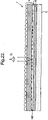
- FIG. 1 illustrates schematically a banknote 1 having a security thread 2 and a transparent window 3.
- the banknote 1 may be made of paper or polymer (such as bi-axially oriented polypropylene) and one or both of the security thread 2 and window 3 incorporates a security device according to the invention.
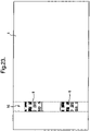
- Figure 2a schematically illustrates the appearance of a comparative example of a security device in plan view.
- the appearance of a moiré magnification device depends on the nature of the microimage element array(s) included in the device, since the device presents a magnified version of the array(s).
- the discussion below will frequently alternate between the appearance of the device itself, such as that shown in Figure 2a , and the arrangement of the underlying microimage element array(s), of which an example is shown in Figure 2b .
- a device's appearance will be illustrated with a solid, bold outline and no background shading whereas illustrations of microimage arrays (and templates on which they are based) will be shown with a broken-line outline and light background shading.
- FIG 2a we show in plan view a comparative example of a security device 10 (here, having a strip format) comprising two alternating sets 11, 12 of synthetically magnified images.
- the selected images are icons, namely the numeral '20' in the first magnified image panel 11, and a 'crest' symbol in the second magnified image panel 12.
- This could represent for example the denominational value of an article to which the device will ultimately be applied and an appropriate regional icon pertaining to the security document.
- the icons are located in separate, non-overlapping zones 11, 12 and are provided in different and preferably contrasting colours, for example red and blue.
- microimage element arrays 100 from which the image panels 11, 12 are generated are shown in Figure 2b .
- Pertaining to each respective image panel 11, 12 will be an array or lattice 110, 120 of microimage elements printed or otherwise formed in the respective colour and at its respective pitch.
- Each microimage array 110, 120 is formed in a separate working: thus, in one example, array 110 consisting of red "20" symbols is laid down before the blue "crest" symbols of array 120.
- Figure 2c shows an enlarged, exemplary portion of the device 10 and its underlying microimage arrays, using a magnification factor M of ⁇ 10.
- M magnification factor
- the positioning of the microfocusing elements 22 relative to the microimage elements is such that, above each array 110, 120, the full magnified version of the element symbol 11, 12 is visible; the magnified "20" numeral 11 of the first array 110 above a notional interface line dividing the two image panels, and the magnified "crest” symbol 12 below the line.
- any visible interference between the image panels 11, 12 is avoided by forming the underlying microimage element arrays 110, 120 in accurate register with one another. That is, the maximum registration error between the arrays is less than or equal to 100 microns. Whilst this has proved difficult using conventional techniques, as described below with reference to Figure 19 , the present inventor has devised a method through which this is possible. Since the respective microimage arrays 110, 120 can be accurately placed relative to one another, overlapping of the resulting image panels 11, 12 is minimised and there is no visible interference or obscuration of one array by the other. In practice there may be a very small overlap between the two arrays but, as discussed above, this will not be resolvable to the human eye. This leads to the significant benefit that there is no need for complex design rules pertaining to each microimage element array and in fact both image arrays could in one case be comprised of the same symbol type differentiated only by colour.
- the pitch of both respective image arrays is the same such that the two synthetically magnified image panels 11, 12 will appear to be located on the same plane some distance behind or in front of the device.
- the two image panels 11, 12 located on different image planes and which is achieved through the use of different microimage element array pitches as will be discussed further below.
- the synthetic image panel generated by any one of the respective micro element arrays could include areas appearing to lie in more than one plane using methods already known in the art (see for example EP-A-1695121 ) - for example alternate elements of the magnified '20's' image array may be provided on two separate image planes.
- the two microimage arrays in accurate register ensures that, when the device is viewed, there is no visible interference (i.e. overlap) between the image panels. This results in a distinctive visual appearance and hence the device is effective for many applications. However, the device may yet suffer from other distracting effects when viewed at different angles or even along the normal if there is mis-register between the microimage arrays and the microfocusing element array.
- Figure 2 relates to a discrete alternating colour array device in which the position of each microimage array relative to the focusing element array and / or the particular viewing direction ensures that the magnified image elements sit wholly within their respective microimage arrays. That is, the synthetically magnified versions of the "20" icons and "crest” symbols sat centrally within each image panel - in other words, there was no loss of design / image continuity across the panel boundaries.
- Figure 3 shows a more typical scenario in Figure 3 , in which the same level of control is not achieved.
- Figures 3a and 3b show a section of the same device as that depicted in Figure 2 , but wherein a vertical displacement of the magnified image elements 11, 12 relative to their associated micro image array panels 110, 120 has occurred either due to a change in viewing angle, or due to a vertical shift in the registration of the micro focussing element array 22 relative to the two microimage arrays 110 and 120.
- mis-register between the micro-focusing element (e.g. microlens) array and the microimage element arrays is prohibitively difficult to eliminate.
- Figure 3(c)(i) shows with a cross the position (labelled 120*) where the microimage array 120 is in register with the focussing array 22, and here we see that the magnified image 12 is centered about that position - hence enabling the full magnified image 12 to be seen, which corresponds to the scenario in Figure 2 ).
- Figure 3(c)(ii) shows the scenario where the position or register of the microimage array 120 is moved up by a registration error ⁇ , which here corresponds to half the height of one of the "crest" microimage elements.
- the new location 120* of mutual register between the microimage array and microfocusing array is again marked with a cross.
- the magnified image 12 has been caused to move up so that its artwork center is located over the new register location 120*.
- the present invention also provides techniques whereby problems arising from unavoidable registration errors are eliminated - that is, eliminating visual effects which would otherwise be generated when the adjacent printed micro image panels do not maintain mutual register and thus do not accurately butt up to each other (as was shown in Fig 2b ), as well as alleviating those arising from mis-register between the micro-focussing elements and the microimage elements.
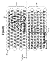
- FIG. 4 An example of microimage array mis-registration is shown in Figure 4 , wherein we see that the central microimage array 110 (corresponding to the image panel 11 with "20" icons) of the microimage element array 100 has shifted downwards relative to the two "crest" arrays 120' and 120" - causing a gap G to appear unintentionally between the arrays 110 and 120", and of more concern it causes an overlap OV of the two micro image arrays 110 and 120' in the lower image zone. This results in an uncontrolled overlap which is disturbing to the viewer and thus uncontrolled interference between the two synthetically magnified image panels 11, 12 leading to a loss or reduction in image integrity.
- Figure 4(b) shows an enlarged portion of the Figure 4 device in the region of the gap G between microimage arrays 110 and 120", where the position or register of the upper micro image array 120" is shifted upwards or away from the lower array 110 such that a gap or void is created in the transition zone between the two arrays.
- a void to be visually tolerated by the observer it is desirable that its width be appreciably less than the vertical dimensions of the magnified images 11, 12 and their associated inter image gap
- Figure 4(b) shows a further enlarged portion of the Figure 4 device in the region of the overlap OV between microimage arrays 110 and 120'.
- this Figure illustrates both the magnified image elements 11, 12 and the microimage element arrays 110, 120 but in practice only the magnified images will be visible. Due to the lower microimage array 120' having been applied out of register with the upper array 110, the lower array shifts up to cross the notional interface and overlaps or collides with the upper micro image array. Since the overlap is between two uncorrelated image arrays, the effect of one array is to compete with and mask the other - i.e the two arrays interfere in an uncooperative way producing a magnified image zone or band with uncontrolled image contributions from each array.
- an interruption zone between the magnified image panels 11, 12 in which no magnified version of either of the microimage arrays is generated. This eliminates any overlap of the magnified images and thus alleviates the above-noted problems. Note that this can be achieved either through modification of the microimage arrays or through modification of the microfocusing element array (both of which options will be detailed below), and in the latter case, there is no requirement to eliminating overlapping of the microimage element arrays themselves.
- An interruption zone is preferably provided along the device at each position where the image changes between one colour and the next: e.g. in the above described examples, an interruption zone would be provided at every interface between image panels 11 and image panels 12.
- Each interruption zone can be generated either by incorporating a boundary region into the design of the microimage element array(s) 100 or by incorporating a "gap" in the micro-focussing element array, or both.
- the device incorporates an interruption zone between adjacent image panels 11, 12 which is formed through the provision of a boundary region between the first and second microimage element arrays 110, 120 which is free from microimage elements associated with either adjacent array.
- Figure 5a shows an example of a design template D which could be used to form the microimage element arrays on the device (e.g. by controlling a printing apparatus in accordance with the template) in the first embodiment. If the microimage element arrays can be formed on the device according to the template with zero registration error, the resulting microimage element arrays would be identical to the design template (however as already indicated and as will be demonstrated below this is typically not the case).
- the design template D includes a boundary region 150 between "first" microimage element array 120' and “second” microimage element array 110, and another between “second” microimage element array 110 and "third” array 120".
- the width of this boundary region 150 in the design template (which is denoted 2 ⁇ ) preferably exceeds the relative register (i.e. the registration error, ⁇ ) with which the microimage element arrays can be formed (e.g. printed) relative to one another, noting that the first and third arrays 120', 120" will be formed in one working whereas the second array 110 will be formed in another.
- the registration error ⁇ of the arrays relative to one another we expect using techniques known in the art will vary from as little as 25 microns to as much as 1000 microns or more.
- the design width 2 ⁇ of the boundary region 150 may be between 25 and 3000 microns. Within that range, the design width is preferably at least 50 microns, more preferably 100 microns. However, to reduce the visual impact of the interruption zone, preferably the design width is no more than 1500 microns, more preferably no more than 1000 microns, still preferably no more than 300 microns, most preferably no more than 150 microns. In one example, the design width is between 100 and 200 microns. In another preferred example, the design width is between 0.05mm and 0,25 mm. However, from a design perspective the width of the boundary region is desirably minimised to reduce its impact on the appearance of the device.
- the design width of the boundary region be-is greater than the pitch A of the microimage elements in the relevant direction (here, A y ). It will be noted that Figure 5 is not to scale in this respect particularly.
- boundary region 150 may also be adjusted to take into account symmetry in the device. How much the width of the boundary region must exceed the inter array print registration error ⁇ to take device symmetry into account will now be considered with reference to Figure 5 . This is particularly of relevance when the device includes at least three microimage element arrays, with the middle array being formed in a different working from those on either side, such as is the case for arrays 110, 120' and 120".
- Figure 5a shows the design template D which is identical to the mircoimage element arrays 100 if the arrays are laid down on the device in strict mutual register.
- the boundary regions 150 between the adjoining zones of alternating colour are each defined by a micro-image free zone of width 2 ⁇ .
- Figure 6 shows the microimage element arrays formed on the device.
- Figure 6a we the have scenario where the partial boundary regions associated with each printed panel butt up and thus the two colour panels are deemed to be in mutual register.
- the finished (e.g. printed) arrays appear identical to the design template of Figure 5a .
- the actual boundary region 150' between the finished arrays 110 and 120" increases to (2 ⁇ + ⁇ ), whilst in the lower transition zone the width of boundary region 150" is reduced to (2 ⁇ - ⁇ ).
- the arrays formed on the device are not identical to the design template D on which they are based (at least in terms of inter-array registration).
- the ratio ⁇ will have a value which generally satisfies the condition ⁇ ⁇ 1.0.
- the registration variance ⁇ has a minimum value set by engineering limits of the manufacturing system, and the boundary width has a maximum value set by the need for its size to harmonise with the synthetically magnified image array.
- a typical registration tolerance ⁇ between sequential print heads in a modern polymer web based print system is of order of ⁇ 0.15 mm.
- the dimensions of the thread window set a scale for the size of the magnified image elements and their repeat spacing. Let us assume the windows dimensions have a typical value 3-4 mm in width by 4-6 mm in height. Then the optical device designer will choose a magnified image size circa 2-3m mm and with an image repeat less than 4mm.
- the finished boundary region width should be preferably less than the dimension of the magnified image elements and their respective inter image gaps, such that the void zone appears to naturally fit with the remainder of the device imagery.
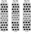
- Figures 7 to 9 illustrate the validity of our symmetry criteria.
- registration error causes the inter array gap to increase and decrease by 25% at both respective array boundaries.
- the asymmetry is less obvious than in previous example but is still readily discernable.
- the registration error creates a level of boundary asymmetry which is barely discernable on initial inspection and therefore would not trouble or distract the viewer. This therefore represents a preferred embodiment.
- the inventors have created a design rule which states that the boundary region design width 2 ⁇ must be as a minimum some 9 times that of the value of the register error. This applies when the registration variance ⁇ is of a size that can be visualised by the naked eye - which is generally greater than 100um or 150um for a normally sighted person
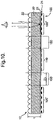
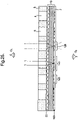
- Figure 10 illustrates in cross-section a general overall structure of any of the devices 10 referred to above in connection with Figures 2 to 9 .
- the device is depicted as a two-colour moiré magnifier operating via transmissive lenses - these lenses maybe spherical (2D moire) or cylindrical (1D moire) as explained further below.
- the device 10 comprises a transparent substrate comprised typically of PET or Biaxial OPP, on the upper surface of which is formed a two-dimensional array of spherical microlenses 22.
- This array may comprise, for example, clear resin into which is formed the lens array by embossing (the resin in this case is required to have thermoplastic properties) or by the process of cast cure replication (the UV curing process may be free radical or cationic).
- the diameters of the microlenses 22 is typically in the range 1-100 microns, preferably 1-50 microns and even more preferably 10-30 microns, thus defining pitches in a similar range.
- the focal length of the microlenses 22 is substantially equal to the thickness t of the optical spacer layer which in this example comprises the thickness of the substrate 20 plus the thickness of a print receptive layer 21 on the opposite surface of the substrate 20 to the microlens array 22 so as to define a focal plane 24 substantially coincident with the surface of the print receptive layer.
- the microimage element arrays 100 On the print receptive layer 21 is formed the microimage element arrays 100. For example, first the microimage array 110 of '20' icons may be printed as a first working in a red colour. Next, the microimage arrays 120', 120" are printed as a second working in a blue colour. It will be seen in Figure 10 that the arrays are each printed on the print receptive layer 21 coincident with the focal plane 24.
- the print receptive layer 21 is not essential however in practice its presence serves to accommodate for the fact that substrate materials such as PET and BOPP are typically provided in a number of standard thickness's or gauges, most typically 19um and 23um and thus the substrate thickness itself cannot be adjusted or tuned to ensure the print is coincident or coplanar with the focal plane of the lens array.
- the thickness of the transparent print receptive layer is adjusted to ensure that the focal point of the lenses is coincident with the printed micro images subsequently applied to this coating.
- each boundary region 150 is devoid of microimage elements.
- the width of the boundary regions 150 is equal to the design width, 2 ⁇ .
- the width of each boundary region will be (2 ⁇ +/- ⁇ ), where 2 ⁇ is preferably greater than ⁇ so that the formed boundary region has a non-zero width.
- each boundary region 150 is uniformly transparent, carrying no printing or other indicia, although as demonstrated below this need not be the case.
- the boundary regions 150 will prevent interference between the magnified image panels 11, 12 corresponding to the microimage element arrays 110, 120 etc, each image panel being perceived wholly in isolation from the next.
- pitch mismatches are introduced between the microimage arrays 100 and the microlens array 22.
- the mismatch can be the same for each of the arrays 110, 120 but in preferred examples it will be different.
- One method of providing a mismatch is to have a microlens and microimage array with substantially the same pitch where the pitch mismatch is achieved by introducing a small rotational misalignment between the microimage and microlens array.
- the degree of rotational misalignment between the microimage and microlens array is preferably in the range 15° - 0.05°, which results in a magnification range of between ⁇ 4X-1000X for the microimage array. More preferably the rotational misalignment is in the range 2° - 0.1°, which results in a magnification range of between ⁇ 25X-500X for the microimage array.
- microimage array and microlens array are in substantially perfect rotational alignment but with a small pitch mismatch.
- a small pitch mismatch would equate to a percentage increase/decrease of the pitch of the microimage array relative to the microlens array in the range 25% - 0.1%, which results in a magnification range of between ⁇ 4X-1000X for the microimage array.
- the percentage increase/decrease of the pitch of the microimage array relative to the microlens array is in the range 4% - 0.2%, which results in a magnification range of between ⁇ 25X-500X for the microimage array.
- the degree of magnification achieved is defined by the expressions derived in " The Moire magnifier", M. Hutley, R Hunt, R Stevens & P Savander, Pure Appl. Opt. 3 (1994) pp. 133-142 .
- first image panel 11 In a first example suppose we required the first image panel 11 to appear to be located 2mm behind the surface plane of the substrate and the second image panel 12 to be located 6mm behind the surface plane (note images behind the surface plane are by definition "virtual" and a more detailed analysis shows them to be non-inverted relative to micro image object array).
- the first image panel 11 In a second example suppose we require the first image panel 11 to be located 2mm in front of the surface plane, whilst the second image panel 12 remains located 6mm behind the surface plane.
- the first image array 11 will form a real inverted image and thus the sign of the magnification will be negative (which follows from assigning a negative value for the image distance v in the previous expression for magnification).
- the first image panel 11 to be located in front of the surface plane (i.e appearing to float) its micro image array 110 must have a pitch larger than the lens pitch. Conversely if the image pitch is less than the lens pitch then the image array will appear to be located below the surface plane.
- the present invention is not limited to any specific type or geometry of microlens, the only requirement being that the microlens can be used to form an image.
- Microlenses suitable for the present invention include those that refract light at a suitably curved surface of a homogenous material such as plano-convex lenslets, double convex lenslets, and fresnel lenses.
- the present invention will comprise spherical microlenses but lenses of any symmetry including cylindrical lenses could be employed. Both spherical and aspherical surfaces are applicable to the present invention. It is not essential for the microlenses to have a curved surface.
- Gradient refractive index (GRIN) lenses image light by a gradual refraction throughout the bulk of the material as a result of small variations in refractive index.
- Microlenses, based on diffraction, such as Fresnel zone plates can also be used.
- GRIN lenses and amplitude or mask based fresnel zone plates enable the surface containing the microlens array to be planar and offers advantage in print receptivity and durability.
- Master microlens arrays can be produced by number of techniques such as photothermal techniques, melt and reflow of photoresist and photoresist sculpture. Such techniques are known to those skilled in the art and are detailed in chapter 5 of "Micro-Optics: Elements, Systems, and Applications” edited by Hans Peter Herzig, published by Taylor and Francis, reprinted 1998 .
- the master microlens structure can then be physically copied by commercially available replication techniques such as hot embossing, moulding or casting.
- microlens structures can be replicated include but are not limited to thermoplastic polymers such as polycarbonate and polymethylmethacrylate (PMMA) for the hot embossing and moulding processes and acrylated epoxy materials curable by heat or radiation for the casting process.
- thermoplastic polymers such as polycarbonate and polymethylmethacrylate (PMMA) for the hot embossing and moulding processes and acrylated epoxy materials curable by heat or radiation for the casting process.
- PMMA polymethylmethacrylate
- the microlens array is replicated via casting into a UV curable coating applied to a carrier polymer film such as PET.
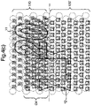
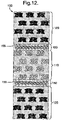
- FIG 11 depicts an example of a microimage element array sequence 100 used in a fifth embodiment of a device.
- first and second microimage element arrays 110, 120 are provided, each being in a different colour and laid down in a different working.
- boundary regions 150 are incorporated between adjacent array pairs.
- each boundary region 150 carries an interruption layer 155.
- the interruption layer 155 is, for example, a printed strip or image pattern formed across the boundary region - this strip being distinct from the adjoining arrays 110, 120 in that there is no micro image array and therefore no corresponding synthetic / moire magnification.
- the interruption layer 155 is shown to have no artwork content.
- the interruption layer can contain design artwork or imagery which could be on a scale which needs a low power magnifier to reveal (e.g. a "teller assist" feature).
- the magnified versions of the adjacent microimage arrays are interrupted or fractioned by the transition (described above with reference to Figure 3 ), they appear to the observer to undergo a predetermined, i.e. design intended, eclipsing event. For example, in some cases the magnified images may appear to move under the stationary boundary region.
- the interruption layer 155 (or "transition band") is preferably applied (e.g. printed) to the structure in tandem with the first moiré (or integral) micro image array 110, i.e. in the same working.
- the interruption layer and the first micro image element array 110 may be present on the same print roller and there is therefore no registration variance between the interruption layer 155 and the first microimage array 110 - in effect the transition band 155 bounds or terminates the first array 110 at either end.
- the transition band at both ends necessarily has the same colour as the first micro image array 110, which may be undesirable.
- the interruption layer could alternatively be applied in a separate working (and in a different colour). Preferably this would be applied before either of the microimage arrays 110, 120.
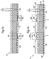
- FIG. 13 shows the device in cross-section, from which it is apparent that the second micro image array 120 may be allowed to overlap or over print the adjacent transitional bands 155. Since the interruption layer is preferably substantially opaque, any overlapped elements are obscured from the observer.
- an interruption layer 155 in the boundary region provides a particularly versatile and practical way of managing the image discontinuity or interference which would otherwise occur across the inter panel boundary.
- the transition band 155 hides the edges of the second print array 120 and thus prevents any visualisation of register error relative to the first print panel, the requirements on the width of the transition band can be relaxed.
- the width of the transition band (which will be the same in the design template and on the finished product, since it is the result of a single working) only needs to exceed the inter panel print register variance, ⁇ . Therefore, in Figure 13 , 2 ⁇ ⁇ 2 ⁇ .
- ⁇ equals say 150um
- the width of the transition band 155 needs to only exceed 300um.
- the interruption zone between the magnified image panels 11, 12 is formed by incorporating a boundary region free from microimage elements in between the microimage arrays.
- Figures 14 and 15 show cross sections of devices according to second and third comparative examples in which this is the case.
- the appearance of the devices in plan view is similar to that of the device shown in Figure 2a (save for the inclusion of "gaps" between the adjacent image panels 11, 12).
- a zone of transition is created in the micro lens array 22 rather than the microimage array 100.
- the microlens array 22 comprises two (or more) arrays 22', 22", 22′′′ etc, separated from each other by boundary regions 250. In these boundary regions 250, the microlenses 22 do not function. This can be achieved using two distinct ways:
- the operation of the lenses is dependent on a refractive index difference between the material of the lens and air. If air is replaced with a resin 255 which has substantially the same refractive index as the polymer material used for the lens 22, the light rays will not be significantly refracted at the resin / lens interface and the micro lenses will not function.
- strips of resin are applied (e.g. printed) over those regions of the micro lens array which are located above the boundaries or transition zones T between the two coloured micro image arrays 110, 120.
- the application of the resin bands 255 to the lenses "switches off" the moiré magnification effect of the lens micro image array 22 in the zone located under the resin band. In short at each panel boundary we create a void in the magnified image pattern whose width is determined by the width of the resin band 255.
- each respective micro image array 110, 120 will still be discernable if the resin 255 is transparent or highly translucent and, as the gap between arrays will alternately increase or decrease by an amount ⁇ at each boundary due to inter panel print mis-register (as explained previously), this may not be desirable from the view point of public recognition.
- uncoloured light scattering pigment such as TiO 2
- the resin band could be incorporated into the design of the feature in which case it may be formed with a (translucent or opaque) colour by incorporating suitable pigments or dyes.
- a different non-transparent coating such as ink could be used in place of resin, and if the level of opacity is sufficiently high, the requirement for the coating's refractive index to match that of the lens material can be relaxed or eliminated.
- the width ⁇ r of this band 255 needs to only exceed the sum of the colour panel print register variation ( ⁇ ⁇ ) and the register variation between the printed resin and the underlying colour panel which we call ⁇ - i.e. ⁇ r ⁇ (2 ⁇ + 2 ⁇ ).
- the boundary region 250 is formed over the inter array boundary T by omitting the micro lenses 22 in that region. In this way, a void zone devoid of micro lenses is created and, once again we have a void zone devoid of magnified images. As before no synthetic imaging will occur within each boundary region 250 and thus the deleterious visual effects associated with inter array register will be much less evident to the observer.
- the boundary region 250 in the lens array 22 may be used to generate the interruption zone alone or in combination with a boundary region 150 between the microimage element arrays 110, 120.
- the microimage array 110, 120 underlying each part 22', 22", 22'" of the microlens array extends laterally beyond the respective part of the microlens array.
- the microimage array 110 extends laterally to the left and right further than the part 22" of microlens array 22 directly above it. The same is true for both arrays 120 and their respective lens arrays 22' and 22"'. This arrangement ensures that the full extent of the microimage array can be viewed when the device is tilted, thereby preventing the magnified images appearing to be "cut off" by the boundary region 250.
- the boundary regions 150 and 250 are depicted as extending in a straight (rectilinear) line across the width of the device.
- the boundary region could be curved or zig-zagged. What is important is that a boundary region exists between the adjacent arrays at least along one axis, which will usually be that axis parallel to the direction in which the substrate travels through the manufacturing process. This is because it is along this direction that registration between two sequential workings cannot be guaranteed: typically, registration in the orthogonal direction will be much more accurate.
- the boundary region may extend along both axis so that any mis-registration along the orthogonal axis is also dealt with.
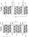
- Figure 16 shows an example of a device having an interruption zone 350 between two image panels 310, 320 (the full set of magnified images is not shown).
- the interruption zone 350 is formed of four areas in staggered positions, resulting in an interlocking pattern. This is formed by providing corresponding boundary zones between the microimage element arrays using the principles of any of the above embodiments.
- the boundary regions only separate one panel from the next along the y-axis direction: the panels abut one another in the x-axis direction at the three circled positions. As indicated above, this is commonly not problematic if the device is formed on a web moving in the y direction only.
- inter panel interruption zone need not be limited to a straight line or rectangular zone but can also be a more complex inter locking pattern.
- the interlocking pattern can again be comprised of linear sections but it also feasible that it may be of curvilinear form - for example an interlocking sinusoid boundary.
- interlocking boundaries make the interruption zone less spatially defined and abrupt, and thereby less readily identified or detected by the observer.
- FIGS 17a and 17b show examples of microimage arrays suitable for use in (a) a 2D device, and (b) a 1D device.
- "empty" boundary regions 150 are incorporated in between the arrays as described with respect to Figure 5 above.
- any of the different boundary regions described in the preceding embodiments could be used instead, whether formed between the micro-image arrays or in the microlens array.
- Figure 17a shows a schematic picture of the respective micro image arrays pertaining to a 2D moiré magnifier device.
- the imaging lenses or mirrors, see below
- the imaging lenses are generally spherical or aspherical in nature with a circular base profile (the profile of the lens or mirror in plan view) and are arranged in a regular two dimensional grid or matrix in the x-y plane as is well known in the art.
- the micro image array is arranged in a grid format which matches that of the lens array. Due to the nature of the lenses, the magnitude of moiré magnification is similar in both the x and y axis and as a consequence the microimage elements are a uniformly scaled down version of their magnified counterparts.
- Figure 17b shows a schematic picture of the respective micro image arrays pertaining to a 1D moiré magnifier device.
- the imaging lenses or mirrors
- moiré magnification occurs only along one axis (the axis of curvature of the lenses), in this case chosen to be the east-west direction. Consequently the microimage elements achieve a high level of magnification along the axis of lens curvature (typically x50 to x200) whilst along the transverse axis they experience a magnification close to unity.
- the corresponding micro images need to highly distorted.
- the micro images have the same height as the same height as the magnified images viewed by the observer, whilst in the transverse east-west direction they are 1/ M times the size of the magnified viewed images (M being the degree of moiré magnification along that axis).
- the microfocusing elements have taken the form of microlenses.
- the security device could alternatively be fabricated as a mirror-based moiré device, of which an example is shown in Figure 18 .
- the spherical microlens array 22 is replaced by a spherical or aspheric concave mirror array 40 formed on one surface of the transparent polymer substrate 20.
- the other surface is provided with printed microimage arrays 110, 120 as before.
- boundary regions 150 are incorporated between each adjacent pair of microimage arrays.
- the interruption zone could instead be generated by disabling a region of the mirror array 40 (e.g. by demetalising or coating).
- a boundary region is incorporated between the microimage element arrays it could include an interruption layer 155 as described with reference to Figures 11 to 13 .
- the focal length of a concave mirror is equal to half its radius of curvature R and therefore can have a limiting minimum value approaching one quarter of the mirror base diameter.
- the focal length and F number of a mirror can be one quarter of the value of equivalent lens (assuming typical refractive index of 1.5).
- reducing F number equates to reducing depth of focus, then in practice it will often be desirable to have a mirror base diameter much less than 2R.
- the base diameter may be 80um
- This structure is intended for viewing only in reflection mode and thus is most relevant for application onto opaque substrates (strip & patch) or partially embedding into opaque substrates (windowed thread).
- the printed micro images must be coincident with the focal plane of the mirrors to a precision determined by the depth of focus or field of the mirror system.
- an interruption layer is to be incorporated, this should preferably be applied to the print receptive layer 23 or substrate 20 first or concurrently with the first microimage array 110, then followed by the application of the second micro image array 120. This ensures that the reflected image pertaining to the interruption layer is visualised as being in front of any elements forming part of the second microimage array which may be applied over the interruption layer doe to mis-registration.
- the incident light has to pass through or be transmitted by the printed micro image arrays 110, 120 (i.e. spatially modulated) before being reflected back as collimated light by the mirror array, then it follows that if the print micro images are substantially opaque the synthetically magnified images will take on a blackish colour or hue against the metallic hue provided by the mirror background. For the synthetically magnified images to appear with the colour of their corresponding micro image array then it is necessary that the micro images are at least partially translucent. The more translucent the micro images the brighter the colour of the synthetic images - however at a cost of reduced image contrast relative to the background. If a interruption layer is included, however, this is preferably substantially opaque to avoid overlying microimage elements being revealed.
- the background hue or colour surrounding the synthetic images will be silver - white or achromat in appearance.
- other affordable coloured metals such as Copper or it alloys maybe be used.
- Other metals such as Silver, Gold, Platinum, Chrome, Nickel, Nickel-Chrome, Palladium, Tin etc may be used where there.
- the microlens array 22 or concave mirror array 40 can be integrally moulded into the polymer substrate 20 or could be formed on the surface of the substrate 20, for example by cast-curing or the like.
- a single micro-image array 110, 120 is used to form each magnified image panel, with the two or more arrays being laterally spaced from one another.
- a third microimage array provided "behind" either or both of the first and second arrays. That is, a third (and possibly fourth, etc) microimage array may be formed which at least partially overlaps with either or both of the arrays 110, 120.
- the third microimage array is provided in a colour different from that of the array(s) it overlaps, and is formed in a separate working.
- the third array is preferably formed at a pitch different from that of the array(s) it overlaps.
- the "depth" of the magnified image perceived by the viewer will depend on the pitch mismatch between the microimage array and the microfocusing element array and as such the magnified version of the third array will appear to lie in a different plane from that of the first and/or second array, thereby avoiding confusion.
- the design might comprise alternating panels of blue "20" symbols (first array 110) and red "crest” symbols (second array 120), with a third common layer of 'stars' or other icons, or a line pattern located behind the first two image arrays.
- the third array could be arranged at a pitch such that its magnified version appears in front of the first and/or second arrays.
- the third array could be printed in an ink that is invisible under normal lighting conditions but visible under UV illumination, in this case the magnified "background" will only be observed under UV illumination.
- either one or both of the first and second arrays 110, 120 could be printed in an ink that changes colour on exposure to UV radiation such that a change in colour of the magnified image is observed under UV radiation.
- Figure 19 illustrates part of an apparatus for printing the microimage element arrays on the substrate.
- the disclosed apparatus greatly reduces the degree of mis-registration between the different microimage element arrays and is therefore particularly suited to producing devices of the type described with respect to Figures 2 and 3 .
- it is also suitable for use in forming devices which include interruption zones as described with reference to any of Figures 5 to 18 above.
- Such devices could alternatively be produced using conventional printing apparatus (e.g. in two print runs, or using a second, offline, printing station), since the width of the interruption zone can be designed to account for the registration error using the principles already discussed. Nonetheless, as already indicated it is preferred that the width of the interruption zone be kept as small as possible so as to reduce its impact on the appearance of the device and so a manufacturing process with very low registration error, such as that now described, is still preferred.
- the apparatus shown in Figure 19 comprises two printing stations 90 and 92 for laying down a first working and a second working, respectively, on substrate 20.
- the substrate is conveyed through the apparatus on a series of tensioning rollers TR1 ... TR4 and travels in the direction indicated by arrow MD (parallel to the y-axis of the substrate).
- a path length adjustment section 91 which can be used to change the length of the substrate transport path between the two printing stations.
- the first printing station 90 comprises an inking roll 70 coupled via a roll chain 72 to an ink reservoir 74. Ink is transferred by the roll 70 onto a print roll 76 carrying recessed printing elements 78 corresponding to the microimage elements of the array concerned. A doctoring blade 84 contacts and removes ink or colorant off the non-recessed areas of the print roller 82.
- the substrate 20 is fed between the print roll 76 and an impression roller 80 and the image elements of the first array 110 are printed onto the substrate 20.
- the second printing station 91 provided downstream of the first, comprises identical components: inking roll 71, roll chain 73, reservoir 75, print roll 77 with recessed elements 79, doctoring blade 85 and impression roller 81, and is used to print the second array 120 of image elements.
- the print stations 90, 92 could include print rolls 76, 77 carrying proud printing elements corresponding to the microimage elements of the array concerned, in which case no doctoring blade 84 is required.
- each respective print roller 76, 78 is provided with printing elements such that only a portion of the roller's circumference imparts micro image print onto the substrate web 20.
- the web carries the first microimage element arrays 110, spaced by empty regions of the web.
- the second microimage element arrays are printed onto the spaces between the first microimage element arrays.
- each print cylinder 76, 77 alternately prints micro image panels of length P onto the web.
- a path length adjusting unit 91 is provided. This comprises a number of web transfer rollers TR1 to TR4 whose action is to adjust the tension of the web in the machine direction MD. Specifically, roller TR3 can move up or down (i.e. out of the plane of the web, in the z-axis), thereby increasing or reducing the path length between the two print stations 90, 92.
- a detector such as camera 95 may be provided downstream of the second print station 92 to detect the size of the inter-array gap (the boundary region) achieved, and supply an error signal corresponding to the magnitude of the detected gap.
- the path length adjusting unit is controlled by a controller (not shown) in response to the error signal provided by the camera system so as to minimise the variation in that gap (i.e. feedback control).
- one or both of the print cylinders 76, 77 could have their position moved transverse to the web direction (i.e. in the x-axis direction) by the action of a transducer provided on the shaft of either roller so that the printed panels have transverse alignment. As discussed above with respect to Figure 16 this assists in the formation of interdigitated interruption zones.
- microlenses or concave micromirrors can be provided on the opposite surface of the substrate 20 by cast-curing, moulding or the like.
- microimage elements have been provided by printing onto the substrate. It would also be possible to provide some or all of the image elements as relief structures and examples of some of these are shown in Figures 13A-13J . In these Figures, 'IM' indicates the parts of the relief generating an image while 'NI' indicates those parts which do not generate an image.
- Figure 13A illustrates embossed or recessed image elements.
- Figure 13B illustrates debossed image elements.
- Figure 13C illustrates image elements in the form of grating structures while Figure 13D illustrates moth-eye or other fine pitch grating structures.
- Figure 13E illustrates image elements formed by gratings in recesses areas while Figure 13F illustrates gratings on debossed areas.
- Figure 13G illustrates the use of a rough embossing.
- Figure 13H illustrates the provision of print on an embossed area while Figure 13I illustrates "Aztec" shaped structures.
- Figure 13J illustrates ink filled recesses.
- FIGS 21 and 22 show an example in which a device 10 made in accordance with any of the preceding embodiments, is applied to an article 1, such as a security document (e.g a banknote, tax stamp, passport stamp, financial card etc.), as an uninterrupted strip or stripe extending from one edge of the article to the other.
- the device 10 may be applied to the document by the application of heat and / or pressure and as such a suitable form of adhesive may be applied to that side of the device which is to be secured to the document substrate.
- a cold adhesive or another transfer method e.g. hot stamping
- the device may be 'rolled' onto the substrate by allowing the device and document to come into contact just prior to passing through a rotary nip wherein the device adhesive may be activated by heat and pressure.
- Figure 22 shows a cross section along line X-X of Figure 21 , illustrating a lens-based embodiment operating in reflection-only mode.
- the device 10 is affixed to the substantially opaque paper or polymer based substrate 5 of article 1 by an adhesive layer 6.
- the synthetically magnified image viewed by the observer O 1 is ultimately derived from light that has been back scattered or reflected from the micro image arrays 100 and the medium that acts as a background to the micro image arrays.
- the greater the reflective contrast between the micro image arrays and the surrounding background medium the greater the visual contrast of the synthetically magnified images.
- the colour or reflective properties of the substrate 5 are non optimal - for example the substrate may be of low reflectivity or a similar colour to one of the micro image arrays.
- the mask layer 7 will typically contain a reflective opacifying pigment such as, but not limited to, titanium dioxide particles in a resin binder.
- the colour of this layer could be simply white or a colorant could be added to ensure that this mask layer or background reflecting layer exhibits a desired hue which contrasts with one or both micro image arrays.
- the mask coat and one of the micro image arrays have overtly the same color, however one or other entity has been provided with a metameric property.
- metameric inks are provided in GB1407065 . Consequently under normal viewing the relevant micro image array is only weakly discerned (if at all) against the background colour of the opaque mask-however when viewed under a metameric filter said micro image array or more pertinently its synthetically magnified image becomes strongly evident.
- the mask coat may be provided with a fluorescent additive such that when viewed under a fluorescent light the mask coat provides a fluorescent background against which the absorbing micro image arrays form black synthetically magnified images.
- the mask coat may also function as a durability enhancing layer.
- the first microimage array 110 could be printed in a first metameric ink and the second array 120 of stars in a second metameric ink where the metameric properties of the inks are such that they appear to be of an identical colour when viewed in daylight, but when viewed in filtered light, the two inks will appear to have different reflective colours.
- a device according to any of the embodiments could be incorporated into a security document as a windowed thread. Examples of such a configuration are shown in Figures 23 , 24 and 25 .
- Figure 23 again a device according to any of the embodiments is provided in or on a security document or other article such a banknote, tax stamp, certificate of authenticity or passport page.
- Windows 8 reveal certain portions of the device 10.
- the device design is not registered to the "north south" (i.e. top and bottom, as shown in the Figure) locations of the substrate windows 9 during the paper or substrate integration process and, as a consequence the manufacturer cannot assure that a particular image panel 11, 12 will wholly and exclusively appear within in a particular window 8.
- the likelihood of ensuring a single panel is present in each window increases when the length of each respective colour panel 11, 12 significantly exceeds the length of the thread window 8 whilst at the same time remaining less than the window repeat distance.
- Figure 24 shows another embodiment wherein the device design or more particularly its vertical colour alternation is registered to the windowed zones 8 in the substrate 1.
- This embodiment is strongly preferred as the presence of a single colour panel 11, 12 in each window provides an unambiguous and easily described security feature which will be quickly appreciated by the viewer.
- the uppermost window 8' reveals only image panel 12, whereas the adjacent window 8" reveals only image panel 11.
- the transition zones where the two image panels meet are located in the non windowed (e.g. fully embedded) portion of the document and are thus hidden from visualisation by the viewer.
- Devices according to any of the above embodiments can be selected for the purpose.
- Figures 25 and 26 show two alternative cross sections along the line Y-Y in Figure 24 (note a different number of windows 8 is depicted but the principles are the same).
- the device 10 is affixed to a surface of the substrate 5 in alignment with windows 8 which pass through the full document thickness.
- the windows 8 may be apertures or could be transparent regions (e.g. polymer) of the substrate 5.
- the windows 8 could formed prior to application of the device 10, or after (e.g. by abrasion).
- the device 10 is affixed to the substrate using any of the techniques previously mentioned with regard to Figures 21 and 22 , and typically an adhesive layer is provided between the microlens array 22 and the substrate.
- a mask layer 7 may be provided as before or may be omitted.
- the device 10 is registered to the substrate 5 using techniques available in the art such that each of the interfaces between adjacent microimage arrays is concealed by the substrate 5 between windows 8.
- Each window 8 is aligned with either the first array 110 or the second array 120.
- the device could operate in both reflection and transmission modes, since the device 10 is applied at least partially over a transparent aperture 8 within the substrate 5.
- the synthetically magnified image may be viewed in reflection and / or transmission through the viewing aperture 8 in the substrate 5.
- the observer will only see magnified image when located in position O 1 . If the opaque mask coat 7 is omitted, the same observer can observe the moiré magnification system in transmission. It is also a requirement that the adhesive layer have good optical clarity (i.e. low scatter, low absorption)
- the printed micro-images 110, 120 are formed from an ink or colorant that is substantially opaque, then the synthetically magnified image will be coloured when viewed in reflection, but will form a high contrast essentially black image when viewed in transmission.
- a requirement for a coloured image to be viewed in transmission is that the micro images must have some degree of translucency. Light must be able to pass through the printed images and the desired colour transmitted. It should be recognised that in regions were the two arrays 110, 120 and therefore magnified images overlap we will have additive colour mixing. For example if the two array colours are red and blue then in areas of overlap the image will be magenta.
- the device 10 is partially embedded within the document. This could be achieved by incorporating the device during papermaking, or laminating it between layers making up the document for example.
- the substrate 5 is now shown in two portions 5a and 5b, one above and one below the device 10.
- both sides of the device 10 will now be provided with an adhesive (only layer 6 is shown, and the same considerations mentioned above regarding index matching of the lenses must be taken into account).
- the windows 8 may be apertures through the first portion of the substrate 5a, formed before or after assembly of the document with the device (e.g. by punching or abrasion), or could be transparent portions of a polymer layer. In this case, if the substrate layer 5b is opaque, the device 10 will only be viewable in reflection mode from position O 1 .
- the security device also includes one or more other optical security features.
- a moiré magnifier device 10 is formed as described with reference to any of the above embodiments.
- the security device also includes a number of holographic image generating structures 400.
- the holographic image structures 400 can be cast or embossed into the same resin as the microlenses but equally two different resins, one suitable for casting the microlenses and one suitable for embossing a holographic structure could be applied in register.
- the holographic structures could be embossed into a polymeric lacquer positioned on the opposite side of the polymeric layer to the microlenses.
- the holographic generating structures 400 can be in the form of holograms or DOVID image elements.
- the microlenses and the visualisation of the two magnified image arrays is located in a central horizontal band or region of the label whilst the holographic generating structures 400 are located on either side.
- the holographic generating structures 400 could be located in a central band or strip with the moiré magnifier 10 being provided in one or more regions on either side.
- moiré magnified images and the image provided by the holographic generating structures could be integrated into a single image by each providing components of a single image.
- Figure 28 illustrates an example of such an integrated design where the holographic generating structures 401 form a scroll and in the middle of the scroll the holographic structures are replaced with a moiré magnifier 10 to create a moiré magnified image in this case of moving "5"'s and stars.
- the holographic structures 400, 401 can have any conventional form and can be fully or partially metallised.
- the reflection enhancing metallised layer can be replaced with a substantially transparent inorganic high refractive index layer, such as ZnS.
- the security devices shown in the previous Figures are suitable to be applied as labels to secure documents which will typically require the application of a heat or pressure sensitive adhesive to the outer surface of the device which will contact the secure document.
- an optional protective coating/varnish could be applied to the exposed outer surface of the device. The function of the protective coating/varnish is to increase the durability of the device during transfer onto the security substrate and in circulation.
- the security device is preferably prefabricated on a carrier substrate and transferred to the substrate in a subsequent working step.
- the security device can be applied to the document using an adhesive layer.
- the adhesive layer is applied either to the security device or the surface of the secure document to which the device is to be applied.
- the carrier strip can be removed leaving the security device as the exposed layer or alternatively the carrier layer can remain as part of the structure acting as an outer protective layer.
- the security device of the current invention can also be incorporated as a security strip or thread.
- Security threads are now present in many of the world's currencies as well as vouchers, passports, travellers' cheques and other documents. In many cases the thread is provided in a partially embedded or windowed fashion where the thread appears to weave in and out of the paper.
- windowed threads can be found in EP0059056 .
- EP0860298 and WO03095188 describe different approaches for the embedding of wider partially exposed threads into a paper substrate. Wide threads, typically with a width of 2-6mm, are particularly useful as the additional exposed area allows for better use of optically variable devices such as the current invention.
- the device structures shown in any of Figures 2 to 18 could be used as a thread by the application of a layer of transparent colourless adhesive to one or both of the outer surfaces of the device. Careful selection of the optical properties of the adhesive in contact with the microlenses is important.
- the adhesive must have a lower refractive index than the microlens material and the greater the difference in the refractive index between the microlenses and the adhesive the shorter the back focal length of the lenses and therefore the thinner the final security device.
- the security device of the current invention can be made machine readable by the introduction of detectable materials in any of the layers or by the introduction of separate machine-readable layers.
- Detectable materials that react to an external stimulus include but are not limited to fluorescent, phosphorescent, infrared absorbing, thermochromic, photochromic, magnetic, electrochromic, conductive and piezochromic materials.
- Additional optically variable materials can be included in the security device such as thin film interference elements, liquid crystal material and photonic crystal materials. Such materials may be in the form of filmic layers or as pigmented materials suitable for application by printing.
- the security device of the current invention may comprise an opaque layer.
- Figures 29 and 30 show a further security feature in the form of a demetallised image incorporated within a security device of the current invention.
- the magnified image arrays of the device 10 are observed In the central band of the device. This provides a primary security effect due to the strong lenticular type animation.
- the structure of the feature shown in Figure 29 along section A-A is as shown in Figure 10 .
- the print receptive layer 23 has been metallised 410.
- Parts 415 of the metal layer are demetallised to define the demetallised images thus enabling the creation of demetallised indicia which can be viewed in reflective but more preferably transmitted light.
- the metallised layer forming the micromirrors may be extended beyond the micormirrors and then parts of this layer can be demetallised to define demetallised images.
- One way to produce partially metallised/demetallised films in which no metal is present in controlled and clearly defined areas, is to selectively demetallise regions using a resist and etch technique such as is described in US-B-4652015 .
- Other techniques for achieving similar effects are for example aluminium can be vacuum deposited through a mask, or aluminium can be selectively removed from a composite strip of a plastic carrier and aluminium using an excimer laser.
- the metallic regions may be alternatively provided by printing a metal effect ink having a metallic appearance such as Metalstar ® inks sold by Eckart.
- a metallic layer can be used to conceal the presence of a machine readable dark magnetic layer.
- a magnetic material When a magnetic material is incorporated into the device the magnetic material can be applied in any design but common examples include the use of magnetic tramlines or the use of magnetic blocks to form a coded structure.
- Suitable magnetic materials include iron oxide pigments (Fe 2 O 3 or Fe 3 O 4 ), barium or strontium ferrites, iron, nickel, cobalt and alloys of these.
- alloys includes materials such as Nickel:Cobalt, Iron:Aluminium:Nickel:Cobalt and the like.
- Flake Nickel materials can be used; in addition Iron flake materials are suitable. Typical nickel flakes have lateral dimensions in the range 5-50 microns and a thickness less than 2 microns. Typical iron flakes have lateral dimensions in the range 10-30 microns and a thickness less than 2 microns.
- a transparent magnetic layer can be incorporated at any position within the device structure.
- Suitable transparent magnetic layers containing a distribution of particles of a magnetic material of a size and distributed in a concentration at which the magnetic layer remains transparent are described in WO03091953 and WO03091952 .
- the security device of the current invention may be incorporated in a security document such that the device is incorporated in a transparent region of the document.
- the security document may have a substrate formed from any conventional material including paper and polymer. Techniques are known in the art for forming transparent regions in each of these types of substrate.
- WO8300659 describes a polymer banknote formed from a transparent substrate comprising an opacifying coating on both sides of the substrate. The opacifying coating is omitted in localised regions on both sides of the substrate to form a transparent region.
- EP1141480 describes a method of making a transparent region in a paper substrate. Other methods for forming transparent regions in paper substrates are described in EP0723501 , EP0724519 , EP1398174 and WO03054297 .
- One or more of the microimage arrays of the present invention may be printed with inks comprising materials that respond visibly to invisible radiation.
- Luminescent materials are known to those skilled in the art to include materials having fluorescent or phosphorescent properties. It is also well known to use other materials that respond visibly to invisible radiation such as photochromic materials and thermochromic materials.
- photochromic materials and thermochromic materials For example only one of the magnified arrays might be visible in normal daylight conditions with the second magnified image becoming visible only under UV illumination. Alternatively the two magnified arrays could appear the same colour in normal daylight conditions and different colours when viewed using a filter or when viewed under UV illumination.
Claims (16)
- Moire-Vergrößerungseinrichtung, umfassend ein transparentes Substrat, das Folgendes trägt:i) ein regelmäßiges Array von Mikro-Fokussierelementen auf einer ersten Oberfläche, wobei die Fokussierelemente eine Fokalebene definieren;ii) ein entsprechendes erstes Array von Mikro-Bildelementen in einer ersten Farbe, die in einer Ebene angeordnet sind, die im Wesentlichen mit der Fokalebene der Fokussierelemente zusammenfällt; und gekennzeichnet durchiii) ein entsprechendes zweites Array von Mikro-Bildelementen in einer sich von der ersten Farbe unterscheidenden zweiten Farbe, die in einer Ebene angeordnet sind, die im Wesentlichen mit der Fokalebene der Fokussierelemente zusammenfällt, wobei das zweite Array von Mikro-Bildelementen dem ersten gegenüber seitlich versetzt ist,wobei die Teilungen der Mikro-Fokussierelemente und der ersten und zweiten Arrays von Mikro-Bildelementen und ihre relative Anordnung so gestaltet sind, dass das Array von Mikro-Fokussierelementen mit dem ersten und dem zweiten Array von Mikro-Bildelementen zur Erzeugung von jeweiligen vergrößerten Versionen der Mikro-Bildelemente eines jeden Arrays infolge des Moire-Effekts zusammenwirkt,und so, dass eine Unterbrechungszone einer Breite nicht null zwischen der vergrößerten Version des ersten Arrays von Mikro-Bildelementen und der vergrößerten Version des zweiten Arrays von Mikro-Bildelementen wahrgenommen wird, wobei die Unterbrechungszone keine vergrößerte Version eines Arrays von Mikro-Bildelementen aufweist,wobei das erste Array von Mikro-Bildelementen vom zweiten Array von Mikro-Bildelementen lateral durch einen Grenzbereich einer Breite nicht null beabstandet ist, der frei von Mikro-Bildelementen ist, woraus die vom Betrachter wahrgenommene Unterbrechungszone entsteht, undwobei die Breite des Grenzbereichs ohne Mikro-Bildelemente größer ist als die Maximalteilung eines jeden Arrays von Mikro-Bildelementen.
- Einrichtung nach Anspruch 1, wobei der Grenzbereich ohne Mikro-Bildelemente eine Unterbrechungsschicht trägt, die vorzugsweise die Form eines einheitlichen oder gemusterten Aufdrucks oder einer Beschichtung annimmt, wobei im Grenzbereich ohne Mikro-Bildelemente die Unterbrechungsschicht vorzugsweise zwischen dem Substrat und dem ersten und/oder zweiten Array von Mikro-Bildelementen angeordnet ist.
- Einrichtung nach einem der vorhergehenden Ansprüche, wobei die Mikro-Fokussierelemente, wie zum Beispiel kleine sphärische Linsen, kleine Zylinderlinsen, kleine planokonvexe Linsen, kleine doppelkonvexe Linsen, kleine Fresnel-Linsen und Fresnel-Zonenplatten, oder aber konkave Spiegel umfassen.
- Sicherheitseinrichtung umfassend eine Einrichtung nach einem der vorhergehenden Ansprüche, vorzugsweise als Sicherheitsfaden, -etikett oder - flecken ausgebildet.
- Sicherheitseinrichtung nach Anspruch 4, bereitgestellt in einem transparenten Fenster eines Sicherheitsdokuments wie zum Beispiel einer Banknote, eines Personalausweises oder dergleichen.
- Wertartikel mit einer optischen Einrichtung nach einem der Ansprüche 1 bis 5, wobei der Wertartikel vorzugsweise eine Banknote, ein Scheck, ein Reisepass, ein Personalausweis, ein Echtheitszertifikat, eine Fiskalmarke oder ein sonstiges Dokument von Sicherheitswert oder Personalidentität ist.
- Verfahren zur Herstellung einer Moire-Vergrößerungseinrichtung, umfassend in beliebiger Reihenfolge:a) die Bildung eines regelmäßigen Array von Mikro-Fokussierelementen auf einer ersten Oberfläche eines transparenten Substrats, wobei die Fokussierelemente eine Fokalebene definieren;b) auf einer zweiten Oberfläche des transparenten Substrats in einem ersten Arbeitsgang die Bildung eines entsprechenden ersten Arrays von Mikro-Bildelementen in einer ersten Farbe, die in einer Ebene angeordnet sind, die im Wesentlichen mit der Fokalebene der Fokussierelemente zusammenfällt; und gekennzeichnet durchc) auf der zweiten Oberfläche des transparenten Substrats in einem zweiten Arbeitsgang die Bildung eines entsprechenden zweiten Arrays von Mikro-Bildelementen in einer sich von der ersten Farbe unterscheidenden zweien Farbe, die in einer Ebene angeordnet sind, die im Wesentlichen mit der Fokalebene der Fokussierelemente zusammenfällt, wobei das zweite Array von Mikro-Bildelementen dem ersten gegenüber seitlich versetzt ist,wobei die Teilungen der Mikro-Fokussierelemente und der ersten und zweiten Arrays von Mikro-Bildelementen und ihre relative Anordnung so gestaltet sind, dass das Array von Mikro-Fokussierelementen mit dem ersten und zweiten Array von Mikro-Bildelementen zur Erzeugung von jeweiligen vergrößerten Versionen der Mikro-Bildelemente eines jeden Arrays infolge des Moire-Effekts zusammenwirkt, und wobei sie so beschaffen sind, dass die Einrichtung eine Unterbrechungszone einer Breite nicht null zwischen der vergrößerten Version des ersten Arrays von Mikro-Bildelementen und der vergrößerten Version des zweiten Arrays von Mikro-Bildelementen optisch anzeigt, wobei die Unterbrechungszone keine vergrößerte Version eines der Arrays von Mikro-Bildelementen aufweist,wobei das erste Array von Mikro-Bildelementen vom zweiten Array von Mikro-Bildelementen lateral durch einen Grenzbereich beabstandet ist, der frei von Mikro-Bildelementen ist, woraus die vom Betrachter wahrgenommene Unterbrechungszone entsteht, und die Breite des Grenzbereichs ohne Mikro-Bildelemente größer ist als die Maximalteilung eines jeden Arrays von Mikro-Bildelementen.
- Verfahren nach Anspruch 7, wobei das erste und das zweite Array von Mikro-Bildelementen auf dem Substrat gemäß einer Entwurfsschablone gebildet werden, die die gewünschte Anordnung der Mikro-Bildelemente im jeweiligen Array definiert, wobei die Entwurfsschablone einen Grenzbereich einer Entwurfsbreite nicht null 2Δ zwischen dem ersten und dem zweiten Array von Mikrobildelementen umfasst, der keine Mikro-Bildelemente enthält und der nach der Bildung der Arrays auf dem Substrat als ein Grenzbereich erscheint, der die vom Betrachter wahrgenommene Unterbrechungszone erbringt, wobei der so gebildete Grenzbereich eine Breite (2Δ +/- Σ) hat, wobei Σ ein Passfehler der ersten Arrays von Mikro-Bildelementen gegenüber dem zweiten Array von Mikro-Bildelementen ist, der mit der Bildung der Arrays in Schritt (b) und (c) verbunden ist.
- Verfahren nach Anspruch 8, wobei die Entwurfsbreite des Grenzbereichs ohne Mikro-Bildelemente größer ist als die größte Abmessung der einzelnen Mikro-Bildelemente.
- Verfahren nach Anspruch 9, wobei die Entwurfsbreite des Grenzbereichs ohne Mikro-Bildelemente größer ist als die Maximalteilung eines jeden Arrays von Mikro-Bildelementen.
- Verfahren nach einem der Ansprüche 8 bis 10, wobei die Entwurfsbreite des Grenzbereichs ohne Mikro-Bildelemente größer ist als der Passfehler Σ.
- Verfahren nach Anspruch 11, wobei für Werte Σ ≥ 100 Mikron die Entwurfsbreite 2Δ des Grenzbereichs ohne Mikro-Bildelemente nach dem folgenden Ausdruck berechnet wird:

- Verfahren nach Anspruch 11 oder 12, wobei für Werte Σ ≤ 100 Mikron die Breite 2Δ des Grenzbereichs ohne Mikro-Bildelemente mindestens 0,5 Σ und vorzugsweise mindestens Σ beträgt.
- Verfahren nach einem der Ansprüche 8 bis 13, weiter umfassend die Bildung einer Unterbrechungsschicht im Grenzbereich ohne Mikro-Bildelemente, wobei die Unterbrechungsschicht vorzugsweise die Form eines einheitlichen oder gemusterten Bereichs annimmt.
- Verfahren nach Anspruch 14, wobei die Unterbrechungsschicht auf das Substrat aufgebracht wird, bevor das erste und/oder zweite Array von Mikro-Bildelementen gebildet wird/werden.
- Verfahren nach Anspruch 15, wobei die Unterbrechungsschicht im selben Arbeitsgang gebildet wird wie das erste Array von Mikro-Bildelementen und vor der Bildung des zweiten Arrays.
Priority Applications (2)
| Application Number | Priority Date | Filing Date | Title |
|---|---|---|---|
| PL11705995T PL2542424T3 (pl) | 2010-03-01 | 2011-03-01 | Urządzenie powiększenia mory |
| EP14179415.6A EP2811470B1 (de) | 2010-03-01 | 2011-03-01 | Moiré-Vergrößerungsvorrichtung |
Applications Claiming Priority (2)
| Application Number | Priority Date | Filing Date | Title |
|---|---|---|---|
| GBGB1003397.5A GB201003397D0 (en) | 2010-03-01 | 2010-03-01 | Moire magnification security device |
| PCT/GB2011/050399 WO2011107783A1 (en) | 2010-03-01 | 2011-03-01 | Moire magnification device |
Related Child Applications (2)
| Application Number | Title | Priority Date | Filing Date |
|---|---|---|---|
| EP14179415.6A Division EP2811470B1 (de) | 2010-03-01 | 2011-03-01 | Moiré-Vergrößerungsvorrichtung |
| EP14179415.6A Division-Into EP2811470B1 (de) | 2010-03-01 | 2011-03-01 | Moiré-Vergrößerungsvorrichtung |
Publications (3)
| Publication Number | Publication Date |
|---|---|
| EP2542424A1 EP2542424A1 (de) | 2013-01-09 |
| EP2542424B1 EP2542424B1 (de) | 2014-09-24 |
| EP2542424B2 true EP2542424B2 (de) | 2022-04-06 |
Family
ID=42125795
Family Applications (5)
| Application Number | Title | Priority Date | Filing Date |
|---|---|---|---|
| EP11705996.4A Active EP2542420B2 (de) | 2010-03-01 | 2011-03-01 | Moiré-vergrösserungsvorrichtung |
| EP14179415.6A Active EP2811470B1 (de) | 2010-03-01 | 2011-03-01 | Moiré-Vergrößerungsvorrichtung |
| EP11705994.9A Active EP2542423B2 (de) | 2010-03-01 | 2011-03-01 | Moiré-vergrösserungsvorrichtung |
| EP11708074.7A Active EP2542425B2 (de) | 2010-03-01 | 2011-03-01 | Moiré-vergrösserungsvorrichtung |
| EP11705995.6A Active EP2542424B2 (de) | 2010-03-01 | 2011-03-01 | Moiré-vergrösserungsvorrichtung |
Family Applications Before (4)
| Application Number | Title | Priority Date | Filing Date |
|---|---|---|---|
| EP11705996.4A Active EP2542420B2 (de) | 2010-03-01 | 2011-03-01 | Moiré-vergrösserungsvorrichtung |
| EP14179415.6A Active EP2811470B1 (de) | 2010-03-01 | 2011-03-01 | Moiré-Vergrößerungsvorrichtung |
| EP11705994.9A Active EP2542423B2 (de) | 2010-03-01 | 2011-03-01 | Moiré-vergrösserungsvorrichtung |
| EP11708074.7A Active EP2542425B2 (de) | 2010-03-01 | 2011-03-01 | Moiré-vergrösserungsvorrichtung |
Country Status (11)
| Country | Link |
|---|---|
| US (4) | US9070237B2 (de) |
| EP (5) | EP2542420B2 (de) |
| JP (4) | JP6162404B2 (de) |
| CN (4) | CN102869518B (de) |
| AU (4) | AU2011222715C1 (de) |
| CA (4) | CA2791161C (de) |
| ES (3) | ES2519595T3 (de) |
| GB (1) | GB201003397D0 (de) |
| MX (4) | MX2012010057A (de) |
| PL (3) | PL2811470T3 (de) |
| WO (4) | WO2011107782A1 (de) |
Families Citing this family (128)
| Publication number | Priority date | Publication date | Assignee | Title |
|---|---|---|---|---|
| GB201003398D0 (en) * | 2010-03-01 | 2010-04-14 | Rue De Int Ltd | Optical device |
| GB201003397D0 (en) | 2010-03-01 | 2010-04-14 | Rue De Int Ltd | Moire magnification security device |
| IN2014CN02023A (de) | 2011-08-19 | 2015-05-29 | Visual Physics Llc | |
| DE102011112554A1 (de) * | 2011-09-06 | 2013-03-07 | Giesecke & Devrient Gmbh | Verfahren zur Herstellung eines Sicherheitspapiers und Mikrolinsenfaden |
| AU2011101209B4 (en) * | 2011-09-20 | 2012-01-12 | Innovia Security Pty Ltd | A security element and method of producing a security element |
| GB201117523D0 (en) | 2011-10-11 | 2011-11-23 | Rue De Int Ltd | Security devices and methods of manufacture thereof |
| GB201117530D0 (en) | 2011-10-11 | 2011-11-23 | Rue De Int Ltd | Security devices |
| JP2013120354A (ja) * | 2011-12-08 | 2013-06-17 | Dainippon Printing Co Ltd | セキュリティ媒体及びそれを用いた真贋判定方法 |
| DE102012204343A1 (de) * | 2012-03-19 | 2013-09-19 | Bundesdruckerei Gmbh | Verfahren zur Herstellung eines Sicherheitsverbundkörpers und Sicherheitsverbundkörper mit zwei optisch brechenden Strukturen |
| GB201208137D0 (en) * | 2012-05-10 | 2012-06-20 | Rue De Int Ltd | Security devices and methods of manufacture therefor |
| CN102975568B (zh) * | 2012-05-30 | 2014-12-03 | 中钞特种防伪科技有限公司 | 光学防伪元件、使用该光学防伪元件的产品及其制备方法 |
| KR102014576B1 (ko) | 2012-08-17 | 2019-08-26 | 비쥬얼 피직스 엘엘씨 | 미세구조물을 최종 기판에 전사하기 위한 프로세스 |
| JP6061192B2 (ja) * | 2013-02-12 | 2017-01-18 | 独立行政法人 国立印刷局 | 立体表示形成体及びその作製方法 |
| EP2767395A1 (de) * | 2013-02-15 | 2014-08-20 | KBA-NotaSys SA | Substrate für Sicherheitspapiere und Herstellungsverfahren dafür |
| BR112015022369A2 (pt) | 2013-03-15 | 2017-07-18 | Visual Physics Llc | dispositivo de segurança óptica |
| US20140265301A1 (en) | 2013-03-15 | 2014-09-18 | 3M Innovative Properties Company | Security feature utlizing hinge material and biodata page |
| US9243169B2 (en) * | 2013-05-16 | 2016-01-26 | Sicpa Holding Sa | Security laminate |
| GB2514338B (en) | 2013-05-17 | 2020-06-10 | De La Rue Int Ltd | Security documents and methods of manufacture |
| CN103278870B (zh) * | 2013-05-23 | 2015-12-02 | 苏州平流层信息科技有限公司 | 利用菲涅尔透镜制作logo的方法 |
| WO2014201017A1 (en) * | 2013-06-11 | 2014-12-18 | Avery Dennison Corporation | Composite image heat transfer |
| US9873281B2 (en) | 2013-06-13 | 2018-01-23 | Visual Physics, Llc | Single layer image projection film |
| US20140367957A1 (en) * | 2013-06-13 | 2014-12-18 | Ad Lucem Corp. | Moiré magnification systems |
| CN103342060B (zh) * | 2013-06-18 | 2016-01-20 | 坤达国际有限公司 | 一种立体图像印刷品及立体图像印刷工艺 |
| TW201522101A (zh) * | 2013-07-10 | 2015-06-16 | Sicpa Holding Sa | 唯一識別符及有關此唯一識別符之高安全裝置 |
| TW201502257A (zh) * | 2013-07-10 | 2015-01-16 | Sicpa Holding Sa | 包括可印碼與手性液晶聚合物層的標記 |
| GB201313362D0 (en) | 2013-07-26 | 2013-09-11 | Rue De Int Ltd | Security Devices and Methods of Manufacture |
| GB201313363D0 (en) | 2013-07-26 | 2013-09-11 | Rue De Int Ltd | Security devices and method of manufacture |
| JP6349401B2 (ja) * | 2013-09-04 | 2018-06-27 | ルメンコ エルエルシーLumenco, Llc | イメージの2軸活性化を実現するマイクロレンズアレイのためのピクセルマッピング及び印刷 |
| GB201317195D0 (en) | 2013-09-27 | 2013-11-13 | Rue De Int Ltd | Method of manufacturing a pattern and apparatus therefor |
| WO2015082332A1 (de) * | 2013-12-02 | 2015-06-11 | Leonhard Kurz Stiftung & Co. Kg | Verfahren zum authentifizieren eines sicherheitselements und optisch variables sicherheitselement |
| WO2015084872A2 (en) * | 2013-12-03 | 2015-06-11 | Crane & Co., Inc. | A security sheet or document having one or more enhanced watermarks |
| WO2015119675A1 (en) * | 2014-02-10 | 2015-08-13 | Uni-Pixel Displays, Inc. | Optical alignment of multi-station flexographic printing system using moiré interference |
| EP2908341B1 (de) * | 2014-02-18 | 2018-07-11 | ams AG | Halbleitervorrichtung mit oberflächenintegriertem Fokussierelement |
| US10766292B2 (en) | 2014-03-27 | 2020-09-08 | Crane & Co., Inc. | Optical device that provides flicker-like optical effects |
| JP2017522602A (ja) | 2014-03-27 | 2017-08-10 | ビジュアル フィジクス エルエルシー | フリッカー状の光学効果を生成する光学デバイス |
| ES2721757T3 (es) | 2014-07-17 | 2019-08-05 | Visual Physics Llc | Material de lámina polimérico mejorado para su uso en la obtención de documentos de seguridad poliméricos tales como billetes de banco |
| US20160133168A1 (en) * | 2014-11-06 | 2016-05-12 | Sung Jae Cho | Three-dimentional label having moving patterns using fine patterns and microlens |
| AU2015317844B2 (en) | 2014-09-16 | 2019-07-18 | Crane Security Technologies, Inc. | Secure lens layer |
| CN105620066B (zh) * | 2014-11-05 | 2018-03-20 | 中国科学院苏州纳米技术与纳米仿生研究所 | 透明微结构的制造方法 |
| US9971165B2 (en) * | 2014-12-30 | 2018-05-15 | Shenzhen China Star Optoelectronics Technology Co., Ltd. | 3D display apparatus |
| KR101721557B1 (ko) * | 2015-02-05 | 2017-03-30 | 손서경 | 위조방지를 위한 모아레 간섭무늬의 생성구조 |
| WO2016130822A1 (en) | 2015-02-11 | 2016-08-18 | Crane & Co., Inc. | Method for the surface application of a security device to a substrate |
| CN104614790B (zh) * | 2015-03-03 | 2016-06-22 | 苏州苏大维格光电科技股份有限公司 | 平面菲涅尔透镜阵列动态放大光学膜 |
| CN107431739B (zh) * | 2015-03-17 | 2019-11-08 | 爱克发有限公司 | 安全图案生成方法 |
| GB2536877B (en) | 2015-03-23 | 2017-06-28 | De La Rue Int Ltd | Security device and method of manufacture |
| AU2015100385B4 (en) * | 2015-03-26 | 2015-07-02 | Ccl Secure Pty Ltd | An aperiodic moiré security element and method for production thereof |
| GB2552109A (en) * | 2015-03-26 | 2018-01-10 | Ccl Secure Pty Ltd | An aperiodic moiré security element and method for production thereof |
| US11029529B2 (en) | 2015-06-04 | 2021-06-08 | Stephen Y. Chou | Subwavelength structured lens having moire pattern, use and methods of making the same |
| GB2549215B (en) | 2015-06-10 | 2018-07-25 | De La Rue Int Ltd | Security devices and methods of manufacture thereof |
| DE102015008655A1 (de) * | 2015-07-03 | 2017-01-05 | Giesecke & Devrient Gmbh | Sicherheitselement mit farbfilterndem Gitter |
| MA42899A (fr) | 2015-07-10 | 2018-05-16 | De La Rue Int Ltd | Procédés de fabrication de documents de sécurité et de dispositifs de sécurité |
| WO2017035437A1 (en) | 2015-08-27 | 2017-03-02 | Crane Security Technologies, Inc. | Single or dual transfer process for preparing and transfering sharply defined single elements to objects to be protected |
| DE102015218829B4 (de) * | 2015-09-30 | 2018-08-16 | Bayerische Motoren Werke Aktiengesellschaft | Bilderzeugungsvorrichtung und Verfahren zur Herstellung eines Arrays bildgebender Elemente |
| JP6676917B2 (ja) * | 2015-10-07 | 2020-04-08 | 凸版印刷株式会社 | 表示体、および、表示体の真贋判定方法 |
| CA3040656A1 (en) * | 2015-10-19 | 2017-04-27 | Hydra Management Llc | Instant ticket redundancy via multi-chromatic indicia |
| US10377162B2 (en) | 2015-10-19 | 2019-08-13 | Hydra Management Llc | Instant ticket redundancy via multi-chromatic indicia |
| GB201520085D0 (en) | 2015-11-13 | 2015-12-30 | Rue De Int Ltd | Methods of manufacturing image element arrays for security devices |
| CN105479974B (zh) * | 2015-12-01 | 2018-07-13 | 中钞特种防伪科技有限公司 | 一种光学防伪元件及使用该光学防伪元件的光学防伪产品 |
| US10189294B2 (en) | 2015-12-03 | 2019-01-29 | Lumenco, Llc | Arrays of individually oriented micro mirrors for use in imaging security devices for currency and brand authentication |
| DE102015015991A1 (de) * | 2015-12-10 | 2017-06-14 | Giesecke & Devrient Gmbh | Sicherheitselement mit Linsenrasterbild |
| ES2860910T3 (es) * | 2015-12-18 | 2021-10-05 | Visual Physics Llc | Película de proyección de imágenes de una sola capa |
| USD778941S1 (en) * | 2016-01-08 | 2017-02-14 | Apple Inc. | Display screen or portion thereof with graphical user interface |
| GB2549724B (en) | 2016-04-26 | 2019-12-11 | De La Rue Int Ltd | Security devices and methods of manufacturing image patterns for security devices |
| GB2550168B (en) | 2016-05-11 | 2018-07-25 | De La Rue Int Ltd | Security device and method of manufacture |
| JP6855688B2 (ja) * | 2016-05-19 | 2021-04-07 | 株式会社村田製作所 | グラビア印刷版、グラビア印刷方法および電子部品の製造方法 |
| RU2736014C2 (ru) * | 2016-06-14 | 2020-11-11 | Роллинг Оптикс Инновейшн АБ | Синтетическое изображение и способ его изготовления |
| JP6820539B2 (ja) * | 2016-06-14 | 2021-01-27 | 大日本印刷株式会社 | 変位可視化センサー |
| JP6749633B2 (ja) * | 2016-07-11 | 2020-09-02 | 国立大学法人大阪大学 | 分光器、波長測定装置及びスペクトル測定方法 |
| GB201612290D0 (en) | 2016-07-15 | 2016-08-31 | La Rue Int De Ltd | Methods of manufacturing a secuirty device |
| GB2557167B (en) | 2016-09-30 | 2020-03-04 | De La Rue Int Ltd | Security devices |
| JP6256727B2 (ja) * | 2016-12-27 | 2018-01-10 | 大日本印刷株式会社 | セキュリティ媒体が配されたカード、セキュリティ媒体が配された紙 |
| ES2922024T3 (es) | 2017-02-10 | 2022-09-06 | Crane & Co Inc | Dispositivo óptico de seguridad legible por máquina |
| CN108454265B (zh) * | 2017-02-20 | 2023-09-08 | 中钞特种防伪科技有限公司 | 防伪元件及光学防伪产品 |
| GB2562775B (en) * | 2017-05-25 | 2021-06-02 | De La Rue Int Ltd | Holographic security device and method of manufacture thereof |
| GB2562797A (en) | 2017-05-26 | 2018-11-28 | De La Rue Int Ltd | Security device and method |
| KR102519590B1 (ko) * | 2017-06-05 | 2023-04-07 | 크레인 앤 코, 인크 | 플리커-유사 광학 효과를 제공하는 광학 장치 |
| CN107271140B (zh) * | 2017-06-30 | 2019-05-21 | 大连理工大学 | 一种在实验水槽指定位置处产生极端波浪的方法 |
| CN109318618B (zh) * | 2017-07-31 | 2020-11-24 | 中钞特种防伪科技有限公司 | 光学防伪元件与防伪产品 |
| CN109551956B (zh) * | 2017-09-26 | 2021-11-26 | 昇印光电(昆山)股份有限公司 | 装饰片及电子设备盖板 |
| UA127132C2 (uk) * | 2017-09-29 | 2023-05-10 | Сікпа Холдінг Са | Тонкий оптичний захисний елемент і спосіб його виготовлення |
| GB2567165B (en) * | 2017-10-04 | 2020-08-26 | De La Rue Int Ltd | Improvements in security sheets comprising security elements |
| DE102017218801B3 (de) * | 2017-10-20 | 2018-11-15 | Koenig & Bauer Ag | Verfahren zur Herstellung eines Sicherheitselementes oder Sicherheitsdokumentes |
| GB2567680B (en) * | 2017-10-20 | 2022-12-21 | Pulsetech Security Ltd | Holograms |
| DE102018201871B3 (de) | 2018-02-07 | 2018-12-13 | Koenig & Bauer Ag | Anordnung aufweisend ein auf ein Substrat aufgebrachtes Druckbild und eine zumindest Teile des Druckbildes abdeckende optisch abbildende Struktur |
| DE102017218802B3 (de) * | 2017-10-20 | 2018-11-15 | Koenig & Bauer Ag | Verfahren zur Herstellung eines Sicherheitselementes oder Sicherheitsdokuments |
| WO2019076805A1 (de) | 2017-10-20 | 2019-04-25 | Koenig & Bauer Ag | Sicherheitselement oder sicherheitsdokument |
| JP6478076B2 (ja) * | 2017-12-05 | 2019-03-06 | 大日本印刷株式会社 | セキュリティ媒体及びそれを用いた真贋判定方法、セキュリティ媒体が配されたカード、セキュリティ媒体が配された紙 |
| FR3075095B1 (fr) | 2017-12-14 | 2020-02-28 | Oberthur Fiduciaire Sas | Ensemble constitue d'un dispositif de transparence complexe et d'au moins un reseau de micro-images, ainsi que document de securite le comportant |
| DE102017130588A1 (de) * | 2017-12-19 | 2019-06-19 | Giesecke+Devrient Currency Technology Gmbh | Wertdokument |
| WO2019136171A1 (en) | 2018-01-03 | 2019-07-11 | Visual Physics, Llc | Micro-optic security device with interactive dynamic security features |
| DE102018000343A1 (de) | 2018-01-17 | 2019-07-18 | Giesecke+Devrient Currency Technology Gmbh | Sicherheitselement mit Lumineszenz-Motivbereich |
| AU2018100225A4 (en) * | 2018-02-21 | 2018-03-22 | Ccl Secure Pty Ltd | Micro-imagery design integration |
| MX2020013861A (es) | 2018-09-10 | 2021-05-27 | Crane & Co Inc | Documento de seguridad totalmete micro optico. |
| GB2578117B (en) | 2018-10-16 | 2021-06-09 | De La Rue Int Ltd | Security devices and methods for their manufacture |
| GB2578773B (en) | 2018-11-08 | 2022-03-30 | De La Rue Int Ltd | Methods of manufacturing security device components |
| GB2580069B (en) | 2018-12-20 | 2022-06-15 | De La Rue Int Ltd | Security documents and methods of manufacture thereof |
| CN109752862B (zh) * | 2019-01-10 | 2022-03-29 | 浙江理工大学 | 一种彩色图像 |
| GB2584597B (en) | 2019-03-28 | 2023-01-18 | De La Rue Int Ltd | Security device and method of manufacture thereof |
| CN111830726B (zh) * | 2019-04-19 | 2023-03-17 | 昇印光电(昆山)股份有限公司 | 3d成像薄膜 |
| CA3141584A1 (en) | 2019-05-20 | 2020-11-26 | Crane & Co., Inc. | Use of nanoparticles to tune index of refraction of layers of a polymeric matrix to optimize microoptic (mo) focus |
| GB2589818B (en) | 2019-07-12 | 2022-12-14 | De La Rue Int Ltd | Security devices and methods of manufacture thereof |
| US11685180B2 (en) * | 2019-08-19 | 2023-06-27 | Crane & Co., Inc. | Micro-optic security device with zones of color |
| CN112505940B (zh) * | 2019-08-26 | 2023-03-24 | 昇印光电(昆山)股份有限公司 | 一种立体成像光学薄膜 |
| CN112505938B (zh) * | 2019-08-26 | 2022-07-05 | 昇印光电(昆山)股份有限公司 | 立体成像膜 |
| CN112433272A (zh) * | 2019-08-26 | 2021-03-02 | 昇印光电(昆山)股份有限公司 | 光学成像膜 |
| KR102153234B1 (ko) * | 2019-09-26 | 2020-09-07 | 지제이엠 주식회사 | 입체 시트 라벨 |
| GB201913913D0 (en) * | 2019-09-26 | 2019-11-13 | Optrical Ltd | Improvements in and relating to security devices |
| GB2588625B (en) | 2019-10-29 | 2022-12-14 | De La Rue Int Ltd | Method of forming a security device |
| PL3888929T3 (pl) * | 2020-03-31 | 2023-01-16 | Pentacomp Pte. Ltd. | Sposób wytwarzania dyskretyzowanej optycznej mikrostruktury zabezpieczającej na podłożu i podkładka do stosowania w tym sposobie |
| GB2594300A (en) * | 2020-04-22 | 2021-10-27 | De La Rue Int Ltd | Security documents and methods of manufacture thereof |
| JP7468137B2 (ja) | 2020-05-19 | 2024-04-16 | Toppanホールディングス株式会社 | 表示体 |
| CN111572235B (zh) * | 2020-05-21 | 2021-09-14 | 苏州大学 | 一种隐藏式立体成像薄膜 |
| US11577540B2 (en) | 2020-05-29 | 2023-02-14 | Capital One Services, Llc | Financial card with dynamic viewing angles to block card information |
| CN111554195B (zh) * | 2020-05-30 | 2022-06-14 | 京东方科技集团股份有限公司 | 柔性显示模组及其制备方法、电子设备 |
| WO2022053828A1 (en) | 2020-09-11 | 2022-03-17 | De La Rue International Limited | Security devices and methods of manufacture thereof |
| JP2022055476A (ja) * | 2020-09-29 | 2022-04-08 | 凸版印刷株式会社 | 表示体 |
| GB2592719B (en) * | 2020-12-15 | 2024-01-17 | Koenig & Bauer Banknote Solutions Sa | Methods for designing and producing a security feature |
| GB2602796B (en) * | 2021-01-11 | 2023-08-23 | De La Rue Int Ltd | Optical devices and methods of manufacture thereof |
| GB202101267D0 (en) | 2021-01-29 | 2021-03-17 | De La Rue Int Ltd | Security devices and methods of manufacture thereof |
| DE102021001019A1 (de) | 2021-02-25 | 2022-08-25 | Giesecke+Devrient Currency Technology Gmbh | Sicherheitselement, Datenträger und Herstellungsverfahren |
| BR112023018101A2 (pt) * | 2021-03-08 | 2023-10-31 | Crane & Co Inc | Dispositivo de segurança micro-óptica com estrutura de ícones multifásica |
| WO2023023453A1 (en) * | 2021-08-16 | 2023-02-23 | Crane & Co., Inc. | Micro-optic security device with enhanced wet-harvest resistance |
| CA3143656A1 (en) * | 2021-12-22 | 2023-06-22 | Bank Of Canada | Dynamic micro-optic security devices, their production and use |
| WO2023170132A1 (en) | 2022-03-10 | 2023-09-14 | Basf Se | Casting lacquer for screen printing |
| DE102022111099B3 (de) | 2022-05-05 | 2023-06-01 | Koenig & Bauer Ag | Sicherheitsdokument mit einem in seinem Substrat ausgebildeten transparenten Fenster |
| DE102022111098B3 (de) | 2022-05-05 | 2023-06-01 | Koenig & Bauer Ag | Druckmaschine zur Herstellung eines Sicherheitsdokuments |
| DE102022111096B3 (de) | 2022-05-05 | 2023-08-24 | Koenig & Bauer Ag | Verfahren zum Authentifizieren eines Sicherheitsdokuments |
| DE102022111097B3 (de) | 2022-05-05 | 2023-06-01 | Koenig & Bauer Ag | Sicherheitsdokument mit einem in seinem Substrat ausgebildeten transparenten Fenster |
Citations (8)
| Publication number | Priority date | Publication date | Assignee | Title |
|---|---|---|---|---|
| WO2006087138A1 (de) † | 2005-02-18 | 2006-08-24 | Giesecke & Devrient Gmbh | Sicherheitselement und verfahren zu seiner herstellung |
| WO2006125224A2 (en) † | 2005-05-18 | 2006-11-23 | Nanoventions Holdings, Llc. | Image presentation and micro-optic security system |
| WO2008000351A2 (de) † | 2006-06-27 | 2008-01-03 | Giesecke & Devrient Gmbh | Sicherheitselement |
| EP1953002A2 (de) † | 2007-01-30 | 2008-08-06 | OVD Kinegram AG | Sicherheitselement zur Sicherung von Wertdokumenten |
| WO2009156079A1 (de) † | 2008-06-23 | 2009-12-30 | Giesecke & Devrient Gmbh | Sicherheitselement |
| WO2010015382A2 (de) † | 2008-08-05 | 2010-02-11 | Giesecke & Devrient Gmbh | Sicherheitsanordnung |
| EP2475529A2 (de) † | 2009-09-11 | 2012-07-18 | OVD Kinegram AG | Mehrschichtkörper |
| EP2494386A1 (de) † | 2009-10-30 | 2012-09-05 | Arjowiggins Security | Sicherheitselement mit einem substrat mit einer optischen struktur und einem referenzmuster sowie zugehöriges verfahren |
Family Cites Families (54)
| Publication number | Priority date | Publication date | Assignee | Title |
|---|---|---|---|---|
| US3357773A (en) * | 1964-12-31 | 1967-12-12 | Rowland Products Inc | Patterned sheet material |
| GB1407065A (en) | 1972-11-30 | 1975-09-24 | Rue Co Ltd Thomas De | Production of security documents |
| IN157644B (de) | 1981-02-19 | 1986-05-10 | Portals Ltd | |
| CA1272231A (en) | 1981-08-24 | 1990-07-31 | Mario Girolamo | Bank notes and the like |
| US4652015A (en) | 1985-12-05 | 1987-03-24 | Crane Company | Security paper for currency and banknotes |
| GB2204272B (en) | 1987-02-18 | 1991-06-19 | Metal Box Plc | Security documents |
| JP2581142B2 (ja) | 1988-03-29 | 1997-02-12 | 日本鋼管株式会社 | オーステナイト系ステンレス鋼材溶接部の耐硝酸腐食性改善方法 |
| GB9211123D0 (en) * | 1992-05-26 | 1992-07-08 | Amblehurst Ltd | Holographic device |
| DE4314380B4 (de) | 1993-05-01 | 2009-08-06 | Giesecke & Devrient Gmbh | Sicherheitspapier und Verfahren zu seiner Herstellung |
| GB9309673D0 (en) | 1993-05-11 | 1993-06-23 | De La Rue Holographics Ltd | Security device |
| GB2293071B (en) | 1993-05-14 | 1997-09-17 | Worldwide Notific Syst | Apparatus for signalling notice of arrival of a movable carrier |
| AT401365B (de) | 1993-10-11 | 1996-08-26 | Oesterr Nationalbank | Wertpapier |
| DE4334847A1 (de) | 1993-10-13 | 1995-04-20 | Kurz Leonhard Fa | Wertdokument mit Fenster |
| GB9612496D0 (en) | 1996-06-14 | 1996-08-14 | De La Rue Thomas & Co Ltd | Security device |
| JP3338860B2 (ja) | 1996-07-17 | 2002-10-28 | ヤマックス株式会社 | 点描画模様の装飾体 |
| GB9828770D0 (en) | 1998-12-29 | 1999-02-17 | Rue De Int Ltd | Security paper |
| JP2001026175A (ja) * | 1999-07-14 | 2001-01-30 | Sony Corp | 段ボールの印刷方法及び梱包用段ボール |
| JP2003510648A (ja) * | 1999-09-30 | 2003-03-18 | コーニンクレッカ フィリップス エレクトロニクス エヌ ヴィ | レンズ状装置 |
| US6450540B1 (en) † | 2000-11-15 | 2002-09-17 | Technology Tree Co., Ltd | Printed matter displaying various colors according to view angle |
| JP2003039583A (ja) | 2001-07-27 | 2003-02-13 | Meiwa Gravure Co Ltd | 装飾シート |
| DE10163381A1 (de) | 2001-12-21 | 2003-07-03 | Giesecke & Devrient Gmbh | Sicherheitspapier sowie Verfahren und Vorrichtung zu seiner Herstellung |
| GB0209564D0 (en) | 2002-04-25 | 2002-06-05 | Rue De Int Ltd | Improvements in substrates |
| GB2388377B (en) | 2002-05-09 | 2004-07-28 | Rue De Int Ltd | A paper sheet incorporating a security element and a method of making the same |
| EP1398174A1 (de) | 2002-09-10 | 2004-03-17 | Kba-Giori S.A. | Verstärktes Substrat für Wertpapiere |
| US7194105B2 (en) | 2002-10-16 | 2007-03-20 | Hersch Roger D | Authentication of documents and articles by moiré patterns |
| US7429062B2 (en) * | 2002-10-30 | 2008-09-30 | Xerox Corporation | Anti-counterfeiting see-through moire security feature using frequency-varying patterns |
| JP2004317636A (ja) | 2003-04-14 | 2004-11-11 | Sanko Sangyo Co Ltd | 被観察体 |
| JP4337114B2 (ja) | 2003-06-16 | 2009-09-30 | ヤマックス株式会社 | 虚像現出装飾体 |
| EP2311647B1 (de) | 2003-11-21 | 2018-01-10 | Visual Physics, LLC | Mikrooptisches Sicherheits- und Bilddarstellungssystem |
| EA011968B1 (ru) | 2004-04-30 | 2009-06-30 | Де Ля Рю Интернэшнл Лимитед | Защитное устройство |
| DE102004044458B4 (de) | 2004-09-15 | 2010-01-07 | Ovd Kinegram Ag | Sicherheitsdokument |
| DE102004056553B4 (de) * | 2004-11-23 | 2013-03-14 | Giesecke & Devrient Gmbh | Sicherheitsanordnung für Sicherheitsdokumente und Verfahren zum Herstellen der Sicherheitsdokumente |
| JP4590614B2 (ja) * | 2005-01-13 | 2010-12-01 | 独立行政法人 国立印刷局 | 偽造防止印刷物 |
| DE102005007749A1 (de) * | 2005-02-18 | 2006-08-31 | Giesecke & Devrient Gmbh | Sicherheitselement und Verfahren zu seiner Herstellung |
| WO2006102700A1 (en) * | 2005-03-29 | 2006-10-05 | Note Printing Australia Limited | Tamper evident identification documents |
| CN101223037B (zh) | 2005-07-12 | 2010-06-23 | 来百客有限公司 | 立体视觉板构造体 |
| ATE413287T1 (de) * | 2005-09-20 | 2008-11-15 | Alcan Tech & Man Ltd | Gegenstand mit optischem effekt |
| DE102005062132A1 (de) * | 2005-12-23 | 2007-07-05 | Giesecke & Devrient Gmbh | Sicherheitselement |
| KR20090028523A (ko) | 2006-05-12 | 2009-03-18 | 크레인 앤드 캄파니 인코퍼레이티드 | 진품 문서 또는 라벨 단독으로 또는 함께, 정적 이미지 및/또는 그외 다른 투사 이미지와 공간적으로 조화를 이루고 움직이는 마이크로-광학 필름 구조 |
| DE102006029852A1 (de) † | 2006-06-27 | 2008-01-03 | Giesecke & Devrient Gmbh | Verfahren zum Aufbringen einer Mikrostruktur, Werkzeugform und Gegenstand mit Mikrostruktur |
| KR101376434B1 (ko) | 2006-06-28 | 2014-04-01 | 비쥬얼 피직스 엘엘씨 | 마이크로-광학 보안 및 화상 표시 시스템 |
| JP2008012870A (ja) * | 2006-07-07 | 2008-01-24 | Grapac Japan Kk | 立体視シート構成体 |
| US20080258457A1 (en) | 2006-09-08 | 2008-10-23 | De La Rue International Limited | Method of manufacturing a security device |
| BE1017460A6 (nl) * | 2007-02-09 | 2008-10-07 | Leo Vermeulen Consulting Lvc | Lenticulair folie. |
| DE102007029204A1 (de) | 2007-06-25 | 2009-01-08 | Giesecke & Devrient Gmbh | Sicherheitselement |
| DE102007029203A1 (de) * | 2007-06-25 | 2009-01-08 | Giesecke & Devrient Gmbh | Sicherheitselement |
| JP5233227B2 (ja) * | 2007-09-28 | 2013-07-10 | 凸版印刷株式会社 | 表示体及びラベル付き物品 |
| DE102008016795A1 (de) | 2008-04-02 | 2009-10-08 | Giesecke & Devrient Gmbh | Verfahren zum Erzeugen einer mikrooptischen Moiré-Vergrößerungsanordnung |
| JP4953026B2 (ja) * | 2008-04-23 | 2012-06-13 | ヤマックス株式会社 | 装飾体 |
| WO2009139396A1 (ja) | 2008-05-01 | 2009-11-19 | 独立行政法人 国立印刷局 | 画像形成体、真偽判別具及び真偽判別方法 |
| US20110233918A1 (en) | 2008-11-18 | 2011-09-29 | Rolling Optics Ab | Time integrated integral image device |
| CN101434176B (zh) * | 2008-12-25 | 2012-11-07 | 中钞特种防伪科技有限公司 | 光学防伪元件及带有该光学防伪元件的产品 |
| GB0919108D0 (en) | 2009-10-30 | 2009-12-16 | Rue De Int Ltd | Security device |
| GB201003397D0 (en) | 2010-03-01 | 2010-04-14 | Rue De Int Ltd | Moire magnification security device |
-
2010
- 2010-03-01 GB GBGB1003397.5A patent/GB201003397D0/en not_active Ceased
-
2011
- 2011-03-01 US US13/580,797 patent/US9070237B2/en not_active Expired - Fee Related
- 2011-03-01 WO PCT/GB2011/050398 patent/WO2011107782A1/en active Application Filing
- 2011-03-01 AU AU2011222715A patent/AU2011222715C1/en active Active
- 2011-03-01 ES ES11705995.6T patent/ES2519595T3/es active Active
- 2011-03-01 CN CN201180022006.3A patent/CN102869518B/zh not_active Expired - Fee Related
- 2011-03-01 MX MX2012010057A patent/MX2012010057A/es active IP Right Grant
- 2011-03-01 EP EP11705996.4A patent/EP2542420B2/de active Active
- 2011-03-01 CN CN201180015130.7A patent/CN102869517B/zh not_active Expired - Fee Related
- 2011-03-01 AU AU2011222723A patent/AU2011222723C1/en active Active
- 2011-03-01 PL PL14179415.6T patent/PL2811470T3/pl unknown
- 2011-03-01 JP JP2012555490A patent/JP6162404B2/ja not_active Expired - Fee Related
- 2011-03-01 AU AU2011222714A patent/AU2011222714C1/en active Active
- 2011-03-01 JP JP2012555488A patent/JP5937522B2/ja not_active Expired - Fee Related
- 2011-03-01 EP EP14179415.6A patent/EP2811470B1/de active Active
- 2011-03-01 US US13/580,837 patent/US8908276B2/en not_active Expired - Fee Related
- 2011-03-01 MX MX2012010058A patent/MX2012010058A/es active IP Right Grant
- 2011-03-01 JP JP2012555491A patent/JP6068145B2/ja not_active Expired - Fee Related
- 2011-03-01 CA CA2791161A patent/CA2791161C/en not_active Expired - Fee Related
- 2011-03-01 JP JP2012555489A patent/JP6006122B2/ja not_active Expired - Fee Related
- 2011-03-01 CN CN201180021465.XA patent/CN102858554B/zh not_active Expired - Fee Related
- 2011-03-01 WO PCT/GB2011/050407 patent/WO2011107791A1/en active Application Filing
- 2011-03-01 MX MX2012009918A patent/MX2012009918A/es active IP Right Grant
- 2011-03-01 WO PCT/GB2011/050404 patent/WO2011107788A1/en active Application Filing
- 2011-03-01 PL PL11705996T patent/PL2542420T3/pl unknown
- 2011-03-01 MX MX2012009822A patent/MX2012009822A/es active IP Right Grant
- 2011-03-01 US US13/580,784 patent/US10127755B2/en not_active Expired - Fee Related
- 2011-03-01 EP EP11705994.9A patent/EP2542423B2/de active Active
- 2011-03-01 EP EP11708074.7A patent/EP2542425B2/de active Active
- 2011-03-01 US US13/580,730 patent/US9177433B2/en not_active Expired - Fee Related
- 2011-03-01 ES ES14179415.6T patent/ES2575102T3/es active Active
- 2011-03-01 ES ES11705996.4T patent/ES2519596T3/es active Active
- 2011-03-01 WO PCT/GB2011/050399 patent/WO2011107783A1/en active Application Filing
- 2011-03-01 CA CA2791055A patent/CA2791055C/en not_active Expired - Fee Related
- 2011-03-01 EP EP11705995.6A patent/EP2542424B2/de active Active
- 2011-03-01 AU AU2011222720A patent/AU2011222720C1/en active Active
- 2011-03-01 CA CA2791160A patent/CA2791160C/en not_active Expired - Fee Related
- 2011-03-01 CA CA2791147A patent/CA2791147C/en not_active Expired - Fee Related
- 2011-03-01 PL PL11705995T patent/PL2542424T3/pl unknown
- 2011-03-01 CN CN201180011752.2A patent/CN102844198B/zh not_active Expired - Fee Related
Patent Citations (9)
| Publication number | Priority date | Publication date | Assignee | Title |
|---|---|---|---|---|
| WO2006087138A1 (de) † | 2005-02-18 | 2006-08-24 | Giesecke & Devrient Gmbh | Sicherheitselement und verfahren zu seiner herstellung |
| WO2006125224A2 (en) † | 2005-05-18 | 2006-11-23 | Nanoventions Holdings, Llc. | Image presentation and micro-optic security system |
| WO2008000351A2 (de) † | 2006-06-27 | 2008-01-03 | Giesecke & Devrient Gmbh | Sicherheitselement |
| EP1953002A2 (de) † | 2007-01-30 | 2008-08-06 | OVD Kinegram AG | Sicherheitselement zur Sicherung von Wertdokumenten |
| WO2009156079A1 (de) † | 2008-06-23 | 2009-12-30 | Giesecke & Devrient Gmbh | Sicherheitselement |
| WO2010015382A2 (de) † | 2008-08-05 | 2010-02-11 | Giesecke & Devrient Gmbh | Sicherheitsanordnung |
| EP2475529A2 (de) † | 2009-09-11 | 2012-07-18 | OVD Kinegram AG | Mehrschichtkörper |
| EP2494386A1 (de) † | 2009-10-30 | 2012-09-05 | Arjowiggins Security | Sicherheitselement mit einem substrat mit einer optischen struktur und einem referenzmuster sowie zugehöriges verfahren |
| US20120243744A1 (en) † | 2009-10-30 | 2012-09-27 | Arjowiggins Security | Security element comprising a substrate bearing an optical structure and a reference pattern, and associated method |
Also Published As
Similar Documents
| Publication | Publication Date | Title |
|---|---|---|
| EP2542424B2 (de) | Moiré-vergrösserungsvorrichtung |
Legal Events
| Date | Code | Title | Description |
|---|---|---|---|
| PUAI | Public reference made under article 153(3) epc to a published international application that has entered the european phase |
Free format text: ORIGINAL CODE: 0009012 |
|
| 17P | Request for examination filed |
Effective date: 20120928 |
|
| AK | Designated contracting states |
Kind code of ref document: A1 Designated state(s): AL AT BE BG CH CY CZ DE DK EE ES FI FR GB GR HR HU IE IS IT LI LT LU LV MC MK MT NL NO PL PT RO RS SE SI SK SM TR |
|
| DAX | Request for extension of the european patent (deleted) | ||
| REG | Reference to a national code |
Ref country code: DE Ref legal event code: R079 Ref document number: 602011010096 Country of ref document: DE Free format text: PREVIOUS MAIN CLASS: B42D0015100000 Ipc: B42D0015000000 |
|
| RIC1 | Information provided on ipc code assigned before grant |
Ipc: G02B 3/00 20060101ALI20140203BHEP Ipc: B42D 15/00 20060101AFI20140203BHEP Ipc: G07D 7/20 20060101ALI20140203BHEP Ipc: G07D 7/00 20060101ALI20140203BHEP |
|
| GRAP | Despatch of communication of intention to grant a patent |
Free format text: ORIGINAL CODE: EPIDOSNIGR1 |
|
| INTG | Intention to grant announced |
Effective date: 20140417 |
|
| GRAS | Grant fee paid |
Free format text: ORIGINAL CODE: EPIDOSNIGR3 |
|
| GRAA | (expected) grant |
Free format text: ORIGINAL CODE: 0009210 |
|
| STAA | Information on the status of an ep patent application or granted ep patent |
Free format text: STATUS: THE PATENT HAS BEEN GRANTED |
|
| AK | Designated contracting states |
Kind code of ref document: B1 Designated state(s): AL AT BE BG CH CY CZ DE DK EE ES FI FR GB GR HR HU IE IS IT LI LT LU LV MC MK MT NL NO PL PT RO RS SE SI SK SM TR |
|
| REG | Reference to a national code |
Ref country code: GB Ref legal event code: FG4D |
|
| REG | Reference to a national code |
Ref country code: CH Ref legal event code: EP |
|
| REG | Reference to a national code |
Ref country code: AT Ref legal event code: REF Ref document number: 688436 Country of ref document: AT Kind code of ref document: T Effective date: 20141015 |
|
| REG | Reference to a national code |
Ref country code: IE Ref legal event code: FG4D |
|
| REG | Reference to a national code |
Ref country code: DE Ref legal event code: R096 Ref document number: 602011010096 Country of ref document: DE Effective date: 20141106 |
|
| REG | Reference to a national code |
Ref country code: ES Ref legal event code: FG2A Ref document number: 2519595 Country of ref document: ES Kind code of ref document: T3 Effective date: 20141107 |
|
| REG | Reference to a national code |
Ref country code: SE Ref legal event code: TRGR |
|
| REG | Reference to a national code |
Ref country code: NL Ref legal event code: T3 |
|
| PG25 | Lapsed in a contracting state [announced via postgrant information from national office to epo] |
Ref country code: FI Free format text: LAPSE BECAUSE OF FAILURE TO SUBMIT A TRANSLATION OF THE DESCRIPTION OR TO PAY THE FEE WITHIN THE PRESCRIBED TIME-LIMIT Effective date: 20140924 Ref country code: NO Free format text: LAPSE BECAUSE OF FAILURE TO SUBMIT A TRANSLATION OF THE DESCRIPTION OR TO PAY THE FEE WITHIN THE PRESCRIBED TIME-LIMIT Effective date: 20141224 Ref country code: LT Free format text: LAPSE BECAUSE OF FAILURE TO SUBMIT A TRANSLATION OF THE DESCRIPTION OR TO PAY THE FEE WITHIN THE PRESCRIBED TIME-LIMIT Effective date: 20140924 Ref country code: GR Free format text: LAPSE BECAUSE OF FAILURE TO SUBMIT A TRANSLATION OF THE DESCRIPTION OR TO PAY THE FEE WITHIN THE PRESCRIBED TIME-LIMIT Effective date: 20141225 |
|
| REG | Reference to a national code |
Ref country code: PL Ref legal event code: T3 |
|
| REG | Reference to a national code |
Ref country code: LT Ref legal event code: MG4D |
|
| PG25 | Lapsed in a contracting state [announced via postgrant information from national office to epo] |
Ref country code: LV Free format text: LAPSE BECAUSE OF FAILURE TO SUBMIT A TRANSLATION OF THE DESCRIPTION OR TO PAY THE FEE WITHIN THE PRESCRIBED TIME-LIMIT Effective date: 20140924 Ref country code: RS Free format text: LAPSE BECAUSE OF FAILURE TO SUBMIT A TRANSLATION OF THE DESCRIPTION OR TO PAY THE FEE WITHIN THE PRESCRIBED TIME-LIMIT Effective date: 20140924 Ref country code: CY Free format text: LAPSE BECAUSE OF FAILURE TO SUBMIT A TRANSLATION OF THE DESCRIPTION OR TO PAY THE FEE WITHIN THE PRESCRIBED TIME-LIMIT Effective date: 20140924 Ref country code: HR Free format text: LAPSE BECAUSE OF FAILURE TO SUBMIT A TRANSLATION OF THE DESCRIPTION OR TO PAY THE FEE WITHIN THE PRESCRIBED TIME-LIMIT Effective date: 20140924 |
|
| REG | Reference to a national code |
Ref country code: FR Ref legal event code: PLFP Year of fee payment: 5 |
|
| PG25 | Lapsed in a contracting state [announced via postgrant information from national office to epo] |
Ref country code: PT Free format text: LAPSE BECAUSE OF FAILURE TO SUBMIT A TRANSLATION OF THE DESCRIPTION OR TO PAY THE FEE WITHIN THE PRESCRIBED TIME-LIMIT Effective date: 20150126 Ref country code: IS Free format text: LAPSE BECAUSE OF FAILURE TO SUBMIT A TRANSLATION OF THE DESCRIPTION OR TO PAY THE FEE WITHIN THE PRESCRIBED TIME-LIMIT Effective date: 20150124 Ref country code: EE Free format text: LAPSE BECAUSE OF FAILURE TO SUBMIT A TRANSLATION OF THE DESCRIPTION OR TO PAY THE FEE WITHIN THE PRESCRIBED TIME-LIMIT Effective date: 20140924 Ref country code: RO Free format text: LAPSE BECAUSE OF FAILURE TO SUBMIT A TRANSLATION OF THE DESCRIPTION OR TO PAY THE FEE WITHIN THE PRESCRIBED TIME-LIMIT Effective date: 20140924 Ref country code: SK Free format text: LAPSE BECAUSE OF FAILURE TO SUBMIT A TRANSLATION OF THE DESCRIPTION OR TO PAY THE FEE WITHIN THE PRESCRIBED TIME-LIMIT Effective date: 20140924 |
|
| REG | Reference to a national code |
Ref country code: DE Ref legal event code: R026 Ref document number: 602011010096 Country of ref document: DE |
|
| PLBI | Opposition filed |
Free format text: ORIGINAL CODE: 0009260 |
|
| REG | Reference to a national code |
Ref country code: HU Ref legal event code: AG4A Ref document number: E022808 Country of ref document: HU |
|
| PLAX | Notice of opposition and request to file observation + time limit sent |
Free format text: ORIGINAL CODE: EPIDOSNOBS2 |
|
| 26 | Opposition filed |
Opponent name: GIESECKE & DEVRIENT GMBH Effective date: 20150623 |
|
| PG25 | Lapsed in a contracting state [announced via postgrant information from national office to epo] |
Ref country code: DK Free format text: LAPSE BECAUSE OF FAILURE TO SUBMIT A TRANSLATION OF THE DESCRIPTION OR TO PAY THE FEE WITHIN THE PRESCRIBED TIME-LIMIT Effective date: 20140924 |
|
| PG25 | Lapsed in a contracting state [announced via postgrant information from national office to epo] |
Ref country code: MC Free format text: LAPSE BECAUSE OF FAILURE TO SUBMIT A TRANSLATION OF THE DESCRIPTION OR TO PAY THE FEE WITHIN THE PRESCRIBED TIME-LIMIT Effective date: 20140924 Ref country code: LU Free format text: LAPSE BECAUSE OF FAILURE TO SUBMIT A TRANSLATION OF THE DESCRIPTION OR TO PAY THE FEE WITHIN THE PRESCRIBED TIME-LIMIT Effective date: 20150301 |
|
| PLAF | Information modified related to communication of a notice of opposition and request to file observations + time limit |
Free format text: ORIGINAL CODE: EPIDOSCOBS2 |
|
| REG | Reference to a national code |
Ref country code: IE Ref legal event code: MM4A |
|
| PG25 | Lapsed in a contracting state [announced via postgrant information from national office to epo] |
Ref country code: IE Free format text: LAPSE BECAUSE OF NON-PAYMENT OF DUE FEES Effective date: 20150301 |
|
| PLBB | Reply of patent proprietor to notice(s) of opposition received |
Free format text: ORIGINAL CODE: EPIDOSNOBS3 |
|
| REG | Reference to a national code |
Ref country code: FR Ref legal event code: PLFP Year of fee payment: 6 |
|
| PG25 | Lapsed in a contracting state [announced via postgrant information from national office to epo] |
Ref country code: SI Free format text: LAPSE BECAUSE OF FAILURE TO SUBMIT A TRANSLATION OF THE DESCRIPTION OR TO PAY THE FEE WITHIN THE PRESCRIBED TIME-LIMIT Effective date: 20140924 |
|
| PG25 | Lapsed in a contracting state [announced via postgrant information from national office to epo] |
Ref country code: MT Free format text: LAPSE BECAUSE OF FAILURE TO SUBMIT A TRANSLATION OF THE DESCRIPTION OR TO PAY THE FEE WITHIN THE PRESCRIBED TIME-LIMIT Effective date: 20140924 |
|
| REG | Reference to a national code |
Ref country code: FR Ref legal event code: PLFP Year of fee payment: 7 |
|
| PG25 | Lapsed in a contracting state [announced via postgrant information from national office to epo] |
Ref country code: SM Free format text: LAPSE BECAUSE OF FAILURE TO SUBMIT A TRANSLATION OF THE DESCRIPTION OR TO PAY THE FEE WITHIN THE PRESCRIBED TIME-LIMIT Effective date: 20140924 Ref country code: BG Free format text: LAPSE BECAUSE OF FAILURE TO SUBMIT A TRANSLATION OF THE DESCRIPTION OR TO PAY THE FEE WITHIN THE PRESCRIBED TIME-LIMIT Effective date: 20140924 |
|
| PG25 | Lapsed in a contracting state [announced via postgrant information from national office to epo] |
Ref country code: TR Free format text: LAPSE BECAUSE OF FAILURE TO SUBMIT A TRANSLATION OF THE DESCRIPTION OR TO PAY THE FEE WITHIN THE PRESCRIBED TIME-LIMIT Effective date: 20140924 |
|
| PG25 | Lapsed in a contracting state [announced via postgrant information from national office to epo] |
Ref country code: BE Free format text: LAPSE BECAUSE OF FAILURE TO SUBMIT A TRANSLATION OF THE DESCRIPTION OR TO PAY THE FEE WITHIN THE PRESCRIBED TIME-LIMIT Effective date: 20140924 |
|
| PLAB | Opposition data, opponent's data or that of the opponent's representative modified |
Free format text: ORIGINAL CODE: 0009299OPPO |
|
| R26 | Opposition filed (corrected) |
Opponent name: GIESECKE+DEVRIENT CURRENCY TECHNOLOGY GMBH Effective date: 20150623 |
|
| REG | Reference to a national code |
Ref country code: FR Ref legal event code: PLFP Year of fee payment: 8 |
|
| PGFP | Annual fee paid to national office [announced via postgrant information from national office to epo] |
Ref country code: NL Payment date: 20180214 Year of fee payment: 8 |
|
| PGFP | Annual fee paid to national office [announced via postgrant information from national office to epo] |
Ref country code: CZ Payment date: 20180214 Year of fee payment: 8 |
|
| PG25 | Lapsed in a contracting state [announced via postgrant information from national office to epo] |
Ref country code: MK Free format text: LAPSE BECAUSE OF FAILURE TO SUBMIT A TRANSLATION OF THE DESCRIPTION OR TO PAY THE FEE WITHIN THE PRESCRIBED TIME-LIMIT Effective date: 20140924 |
|
| APBM | Appeal reference recorded |
Free format text: ORIGINAL CODE: EPIDOSNREFNO |
|
| APBP | Date of receipt of notice of appeal recorded |
Free format text: ORIGINAL CODE: EPIDOSNNOA2O |
|
| APAH | Appeal reference modified |
Free format text: ORIGINAL CODE: EPIDOSCREFNO |
|
| APBQ | Date of receipt of statement of grounds of appeal recorded |
Free format text: ORIGINAL CODE: EPIDOSNNOA3O |
|
| PG25 | Lapsed in a contracting state [announced via postgrant information from national office to epo] |
Ref country code: AL Free format text: LAPSE BECAUSE OF FAILURE TO SUBMIT A TRANSLATION OF THE DESCRIPTION OR TO PAY THE FEE WITHIN THE PRESCRIBED TIME-LIMIT Effective date: 20140924 |
|
| APAH | Appeal reference modified |
Free format text: ORIGINAL CODE: EPIDOSCREFNO |
|
| PG25 | Lapsed in a contracting state [announced via postgrant information from national office to epo] |
Ref country code: CZ Free format text: LAPSE BECAUSE OF NON-PAYMENT OF DUE FEES Effective date: 20190301 |
|
| REG | Reference to a national code |
Ref country code: NL Ref legal event code: MM Effective date: 20190401 |
|
| PG25 | Lapsed in a contracting state [announced via postgrant information from national office to epo] |
Ref country code: NL Free format text: LAPSE BECAUSE OF NON-PAYMENT OF DUE FEES Effective date: 20190401 |
|
| PGFP | Annual fee paid to national office [announced via postgrant information from national office to epo] |
Ref country code: AT Payment date: 20200225 Year of fee payment: 10 Ref country code: HU Payment date: 20200203 Year of fee payment: 10 Ref country code: IT Payment date: 20200221 Year of fee payment: 10 Ref country code: PL Payment date: 20200120 Year of fee payment: 10 Ref country code: SE Payment date: 20200310 Year of fee payment: 10 |
|
| PGFP | Annual fee paid to national office [announced via postgrant information from national office to epo] |
Ref country code: ES Payment date: 20200401 Year of fee payment: 10 |
|
| APBU | Appeal procedure closed |
Free format text: ORIGINAL CODE: EPIDOSNNOA9O |
|
| REG | Reference to a national code |
Ref country code: AT Ref legal event code: MM01 Ref document number: 688436 Country of ref document: AT Kind code of ref document: T Effective date: 20210301 |
|
| PG25 | Lapsed in a contracting state [announced via postgrant information from national office to epo] |
Ref country code: AT Free format text: LAPSE BECAUSE OF NON-PAYMENT OF DUE FEES Effective date: 20210301 Ref country code: SE Free format text: LAPSE BECAUSE OF NON-PAYMENT OF DUE FEES Effective date: 20210302 Ref country code: HU Free format text: LAPSE BECAUSE OF NON-PAYMENT OF DUE FEES Effective date: 20210302 |
|
| PUAH | Patent maintained in amended form |
Free format text: ORIGINAL CODE: 0009272 |
|
| STAA | Information on the status of an ep patent application or granted ep patent |
Free format text: STATUS: PATENT MAINTAINED AS AMENDED |
|
| 27A | Patent maintained in amended form |
Effective date: 20220406 |
|
| AK | Designated contracting states |
Kind code of ref document: B2 Designated state(s): AL AT BE BG CH CY CZ DE DK EE ES FI FR GB GR HR HU IE IS IT LI LT LU LV MC MK MT NL NO PL PT RO RS SE SI SK SM TR |
|
| REG | Reference to a national code |
Ref country code: DE Ref legal event code: R102 Ref document number: 602011010096 Country of ref document: DE |
|
| PG25 | Lapsed in a contracting state [announced via postgrant information from national office to epo] |
Ref country code: IT Free format text: LAPSE BECAUSE OF NON-PAYMENT OF DUE FEES Effective date: 20210301 |
|
| PG25 | Lapsed in a contracting state [announced via postgrant information from national office to epo] |
Ref country code: ES Free format text: LAPSE BECAUSE OF FAILURE TO SUBMIT A TRANSLATION OF THE DESCRIPTION OR TO PAY THE FEE WITHIN THE PRESCRIBED TIME-LIMIT Effective date: 20220406 |
|
| PGFP | Annual fee paid to national office [announced via postgrant information from national office to epo] |
Ref country code: GB Payment date: 20230105 Year of fee payment: 13 Ref country code: DE Payment date: 20221230 Year of fee payment: 13 |
|
| REG | Reference to a national code |
Ref country code: ES Ref legal event code: FD2A Effective date: 20230623 |
|
| PG25 | Lapsed in a contracting state [announced via postgrant information from national office to epo] |
Ref country code: ES Free format text: THE PATENT HAS BEEN ANNULLED BY A DECISION OF A NATIONAL AUTHORITY Effective date: 20210302 |
|
| PGFP | Annual fee paid to national office [announced via postgrant information from national office to epo] |
Ref country code: CH Payment date: 20230402 Year of fee payment: 13 |
|
| PGFP | Annual fee paid to national office [announced via postgrant information from national office to epo] |
Ref country code: FR Payment date: 20231229 Year of fee payment: 14 |