EP2542425B1 - Moiré-vergrösserungsvorrichtung - Google Patents
Moiré-vergrösserungsvorrichtung Download PDFInfo
- Publication number
- EP2542425B1 EP2542425B1 EP11708074.7A EP11708074A EP2542425B1 EP 2542425 B1 EP2542425 B1 EP 2542425B1 EP 11708074 A EP11708074 A EP 11708074A EP 2542425 B1 EP2542425 B1 EP 2542425B1
- Authority
- EP
- European Patent Office
- Prior art keywords
- array
- elements
- microimage
- arrays
- micro
- Prior art date
- Legal status (The legal status is an assumption and is not a legal conclusion. Google has not performed a legal analysis and makes no representation as to the accuracy of the status listed.)
- Active
Links
Images


Classifications
-
- G—PHYSICS
- G07—CHECKING-DEVICES
- G07D—HANDLING OF COINS OR VALUABLE PAPERS, e.g. TESTING, SORTING BY DENOMINATIONS, COUNTING, DISPENSING, CHANGING OR DEPOSITING
- G07D7/00—Testing specially adapted to determine the identity or genuineness of valuable papers or for segregating those which are unacceptable, e.g. banknotes that are alien to a currency
- G07D7/20—Testing patterns thereon
- G07D7/202—Testing patterns thereon using pattern matching
- G07D7/207—Matching patterns that are created by the interaction of two or more layers, e.g. moiré patterns
-
- B—PERFORMING OPERATIONS; TRANSPORTING
- B42—BOOKBINDING; ALBUMS; FILES; SPECIAL PRINTED MATTER
- B42D—BOOKS; BOOK COVERS; LOOSE LEAVES; PRINTED MATTER CHARACTERISED BY IDENTIFICATION OR SECURITY FEATURES; PRINTED MATTER OF SPECIAL FORMAT OR STYLE NOT OTHERWISE PROVIDED FOR; DEVICES FOR USE THEREWITH AND NOT OTHERWISE PROVIDED FOR; MOVABLE-STRIP WRITING OR READING APPARATUS
- B42D25/00—Information-bearing cards or sheet-like structures characterised by identification or security features; Manufacture thereof
- B42D25/30—Identification or security features, e.g. for preventing forgery
- B42D25/324—Reliefs
-
- B—PERFORMING OPERATIONS; TRANSPORTING
- B42—BOOKBINDING; ALBUMS; FILES; SPECIAL PRINTED MATTER
- B42D—BOOKS; BOOK COVERS; LOOSE LEAVES; PRINTED MATTER CHARACTERISED BY IDENTIFICATION OR SECURITY FEATURES; PRINTED MATTER OF SPECIAL FORMAT OR STYLE NOT OTHERWISE PROVIDED FOR; DEVICES FOR USE THEREWITH AND NOT OTHERWISE PROVIDED FOR; MOVABLE-STRIP WRITING OR READING APPARATUS
- B42D25/00—Information-bearing cards or sheet-like structures characterised by identification or security features; Manufacture thereof
- B42D25/30—Identification or security features, e.g. for preventing forgery
- B42D25/342—Moiré effects
-
- B—PERFORMING OPERATIONS; TRANSPORTING
- B42—BOOKBINDING; ALBUMS; FILES; SPECIAL PRINTED MATTER
- B42D—BOOKS; BOOK COVERS; LOOSE LEAVES; PRINTED MATTER CHARACTERISED BY IDENTIFICATION OR SECURITY FEATURES; PRINTED MATTER OF SPECIAL FORMAT OR STYLE NOT OTHERWISE PROVIDED FOR; DEVICES FOR USE THEREWITH AND NOT OTHERWISE PROVIDED FOR; MOVABLE-STRIP WRITING OR READING APPARATUS
- B42D25/00—Information-bearing cards or sheet-like structures characterised by identification or security features; Manufacture thereof
- B42D25/30—Identification or security features, e.g. for preventing forgery
- B42D25/351—Translucent or partly translucent parts, e.g. windows
-
- G—PHYSICS
- G07—CHECKING-DEVICES
- G07D—HANDLING OF COINS OR VALUABLE PAPERS, e.g. TESTING, SORTING BY DENOMINATIONS, COUNTING, DISPENSING, CHANGING OR DEPOSITING
- G07D7/00—Testing specially adapted to determine the identity or genuineness of valuable papers or for segregating those which are unacceptable, e.g. banknotes that are alien to a currency
- G07D7/003—Testing specially adapted to determine the identity or genuineness of valuable papers or for segregating those which are unacceptable, e.g. banknotes that are alien to a currency using security elements
-
- B42D2035/20—
-
- B42D2035/44—
-
- G—PHYSICS
- G02—OPTICS
- G02B—OPTICAL ELEMENTS, SYSTEMS OR APPARATUS
- G02B3/00—Simple or compound lenses
- G02B3/0006—Arrays
- G02B3/0037—Arrays characterized by the distribution or form of lenses
- G02B3/0056—Arrays characterized by the distribution or form of lenses arranged along two different directions in a plane, e.g. honeycomb arrangement of lenses
Definitions
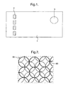
- the invention relates to a moiré magnification device such as a security device, for example for use on security documents and other articles of value such as banknotes, cheques, passports, identity cards, certificates of authenticity, fiscal stamps and other documents for securing value or personal identity. It also relates to optical devices for use on packaging or the like.
- a moiré magnification device such as a security device, for example for use on security documents and other articles of value such as banknotes, cheques, passports, identity cards, certificates of authenticity, fiscal stamps and other documents for securing value or personal identity. It also relates to optical devices for use on packaging or the like.
- Moire magnification has been used as the basis of security devices for a number of years. A number of examples are described in WO-A-94/27254 and EP-A-1695121 .
- a regular array of micro-focusing elements defining a focal plane is provided over a corresponding array of image elements located in a plane substantially aligned with the focal plane of the focusing elements.
- the pitch or periodicity of the array of image elements is chosen to differ by a small factor from the pitch or periodicity of the focusing elements and this mismatch means that magnified versions of the image elements are generated.
- the magnification factor depends upon the difference between the periodicities or pitches.
- a pitch mismatch between a microlens array and a microimage array can also conveniently be generated by rotating the microimage array relative to the microlens array or vice-versa, such that the microlens array and microimage array have a rotational misalignment.
- the rotational misalignment or the small pitch mismatch results in the eye observing a different part of the image in each neighbouring lens resulting in a magnified image. If the eye is then moved relative to the lens/image array a different part of the image is observed giving the impression that the image is in a different position. If the eye is moved in a smooth manner a series of images are observed giving rise to the impression that the image is moving relative to the surface.
- the nature of the movement and orientation changes can be explained from the theory of moiré; this is discussed in detail in " The theory of the Moiré phenomenon” by I. Amidror published by Kluiver Academic Publishers in 2000, ISBN 0-7923-5949-6 .
- the moiré effect of two periodic structures can be explained/predicted by considering the frequency vectors of the two structures.
- the orientation of the frequency vector represents the direction of the periodicity and the length represents the frequency (i.e. 1/Period).
- the vector is expressed by its Cartesian coordinates (u,v) where u and v are the horizontal and vertical components of the frequency.
- the focusing elements comprise microlenses or micromirrors and the image elements are defined by simple icons or the like.
- WO-A-94/27254 illustrates an image switch effect on tilting a device.
- WO-A-2005/106601 describes how two magnified image sets can be caused to move at different rates as the device is tilted. Another example is described in WO-A-2009/139396 .
- a moire magnification device comprises a transparent substrate carrying:
- the first array can appear above or below the second array.
- the device further comprises
- a third array of, typically identical, microimage elements allows the magnified image elements of each array to appear at different depths relative to each other depending upon the pitches of each array.
- the pitches of the array of micro-focusing elements and the first, second and third arrays of microimage elements are chosen such that the magnified version of the first array of microimage elements appears between the magnified versions of the microimage elements of the second and third arrays.
- the pitches of the array of focusing elements and first, second and third arrays of microimage elements are chosen so the magnified version of the image elements of the first array appear above the magnified versions of the image elements of the second and third arrays.
- the microimage elements of at least the first and third arrays may be identical or may morph gradually across the array.
- the invention is particularly advantageous where the background defining the array(s) does not have to be registered with the first array and this can be particularly easily achieved if the background arrays define a respective generic background, for example a line pattern, simple geometric figures, or more complex line structures such as guilloche patterns.
- the microimage elements of at least two of the arrays may only differ in colour.
- the microimage elements of the first, second and third arrays further differ from one another by one or more of shape, size and orientation.
- the microimage elements of at least the first array may typically comprise icons such as symbols, geometric figures, alphanumeric characters and the like and most preferably provide information.
- the microimage elements of one or more of the other arrays may also be formed as icons or more generic patterns as mentioned above.
- the microimage elements are printed on the substrate using any suitable printing process such as gravure, wet or dry lithographic printing, screen printing, intaglio printing and flexo printing.
- any suitable printing process such as gravure, wet or dry lithographic printing, screen printing, intaglio printing and flexo printing.
- one or more of the arrays of microimage elements could also be formed as grating structures, recesses or other relief patterns on the substrate.
- Anti-reflection structures may also be used as described in WO-A-2005/106601 .
- Micro-focusing elements such as microlenses and concave mirrors, are preferably formed by embossing into the substrate surface, cast-curing or the like.
- Moire magnifiers generated by the current invention can be either 2-dimensional (2D) or 1 - dimensional (1D) structures.
- 2D moiré magnification structures using spherical lenses are described in more detail in EP-A-1695121 and WO-A-94/27254 .
- a 2D moiré magnifier the microimages are magnified in all directions.
- a 1D moiré magnification structure the spherical microlenses or micromirros are replaced with a repeating arrangement of cylindrical microlenses or micromirrors. The result of this is that the micro-image elements are subject to moiré magnification in one axis only which is the axis along which the mirrors exhibit their periodic variations in curvature or relief.
- micro-images are strongly compressed or de-magnified along the magnification axis whilst the size or dimension of the micro image elements along the axis orthogonal to the magnification axis is substantially the same as they appear to the observer - i.e. no magnification or enlargement takes place.
- the moiré magnifier generated by the current invention can form a security device by itself but could also be used in conjunction with other security features such as holograms, diffraction gratings and other optically variable effect generating structures.
- the optical device of the current invention can be used to authenticate a variety of substrates - with the nature of the substrate, in particular its thickness and flexibility having an influence on the corresponding properties of the optical device.
- the invention has particular value in protecting flexible substrates such as paper and in particular banknote, where the device could define a patch, strip or thread.
- the thickness of the device will be influenced by how its employed within the banknote though to both avoid deformation of paper ream shape during the banknote printing process and further more the form and flexibility of the banknote itself, it is desirable that the thickness of the device does not exceed half of the thickness of the banknote itself (typically 85-120um)-therefore it anticipated that in any embodiment the optical device will be less than 50um including securing adhesives and preferably substantially so.
- the desired thickness will range from a few microns (excluding securing adhesive) to a maximum of 35 - 40um (again excluding adhesive) for a label. Whilst for the case of a strip, the thickness will range again from a few micrometers for the case of a hot-stamped or transferred strip, up to 35-40um for the case of a non transferred strip wherein the supporting carrier layer is retained (again excluding securing adhesives) as would be necessary should the strip be applied over a mechanical aperture in the banknote substrate.
- final thickness is in the range of 20 -50um.
- Thicker versions of the security device could be employed in applications which include passport paper pages, plastic passport covers, visas, identity cards, brand identification labels, anti-tamper labels--any visually authenticable items.
- the device could be provided in a transparent window of a security document to enable it to be viewed in transmission.
- the focal length of the microlenses 22 is substantially equal to the thickness t of the optical spacer layer which in this example comprises the thickness of the substrate 20 plus the thickness of a print receptive layer 21 on the opposite surface of the substrate 20 to the microlens array 22 so as to define a focal plane 24 substantially coincident with the surface of the print receptive layer.
- the microimage array of '5' icons 10A is first printed on the print receptive layer 21 in a red colour.
- the background array 11 is printed in a blue colour. It will be seen in Figure 10 that the two arrays are each printed on the print receptive layer 21 coincident with the focal plane 24 although the background print 11 also overlaps the '5' icon array 10 as shown at 25.
- the present invention is not limited to any specific type or geometry of microlens, the only requirement being that the microlens can be used to form an image.
- Microlenses suitable for the present invention include those that refract light at a suitably curved surface of a homogenous material such as plano-convex lenslets, double convex lenslets, and fresnel lenses.
- the present invention will comprise spherical microlenses but lenses of any symmetry including cylindrical lenses could be employed. Both spherical and aspherical surfaces are applicable to the present invention. It is not essential for the microlenses to have a curved surface.
- Gradient refractive index (GRIN) lenses image light by a gradual refraction throughout the bulk of the material as a result of small variations in refractive index.
- Microlenses, based on diffraction, such as Fresnel zone plates can also be used.
- GRIN lenses and amplitude or mask based fresnel zone plates enable the surface containing the microlens array to be planar and offers advantage in print receptivity and durability.
- Master microlens arrays can be produced by number of techniques such as photothermal techniques, melt and reflow of photoresist and photoresist sculpture. Such techniques are known to those skilled in the art and are detailed in chapter 5 of "Micro-Optics: Elements, Systems, and Applications” edited by Hans Peter Herzig, published by Taylor and Francis, reprinted 1998.
- the master microlens structure can then be physically copied by commercially available replication techniques such as hot embossing, moulding or casting.
- microlens structures can be replicated include but are not limited to thermoplastic polymers such as polycarbonate and polymethylmethacrylate (PMMA) for the hot embossing and moulding processes and acrylated epoxy materials curable by heat or radiation for the casting process.
- thermoplastic polymers such as polycarbonate and polymethylmethacrylate (PMMA) for the hot embossing and moulding processes and acrylated epoxy materials curable by heat or radiation for the casting process.
- PMMA polymethylmethacrylate
- the microlens array is replicated via casting into a UV curable coating applied to a carrier polymer film such as PET.
- a pitch mismatch is introduced between the microimage array and the microlens array.
- One method is to have a microlens and microimage array with substantially the same pitch where the pitch mismatch is achieved by introducing a small rotational misalignment between the microimage and microlens array.
- the degree of rotational misalignment between the microimage and microlens array is preferably in the range 15°- 0.05°, which results in a magnification range of between ⁇ 4X-1000X for the microimage array. More preferably the rotational misalignment is in the range 2° - 0.1°, which results in a magnification range of between -25X-500X for the microimage array.
- microimage array and microlens array are in substantially perfect rotational alignment but with a small pitch mismatch.
- a small pitch mismatch would equate to a percentage increase/decrease of the pitch of the microimage array relative to the microlens array in the range 25% - 0.1%, which results in a magnification range of between ⁇ 4X-1000X for the microimage array.
- the percentage increase/decrease of the pitch of the microimage array relative to the microlens array is in the range 4%-0.2%, which results in a magnification range of between -25X-500X for the microimage array.
- the degree of magnification achieved is defined by the expressions derived in " The Moire magnifier", M. Hutley, R Hunt, R Stevens & P Savander, Pure Appl. Opt. 3 (1994) pp.133-142 .
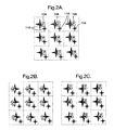
- Figures 2a-2c show the second array 11 in different registration positions relative to the first array 10.
- the key point is that the design and choice of the first and second array elements or icons 10A, 11A is such that there is no significant change in information, content, symbolic relevance or aesthetic appearance when the position of one array is varied relative to the other - in other words the two arrays are not registration sensitive or have a strongly preferred register requirement.
- icon types which are especially information bearing, for example a denominational or alphanumeric symbol or such like are located in the first array 10 which is visualised as being in front of the second array 11.
- each unit cell 11A of the second array 11 is comprised of two identical icons i.e. a large and small star -as a consequence, in informational terms there is a redundancy of information in each unit cell.
- This redundancy property means that if at some relative registration between the two arrays the icon pattern from the first array (the 5's) substantially obscures the array of larger stars, then the smaller star icon array can be readily visualised without significant obscurement or interference from the first array.
- the describable optically variable effect is insensitive (i.e. substantially invariant) to uncontrolled manufacturing variations in the register of the first icon array 10 to the second array 11. This is an important aspect of this invention.
- Figures 2 & 10 were comprised of micro lenses 22 with a focal length f of 40 ⁇ m or 0.04mm. Furthermore let us suppose both the micro lenses and the supporting substrate 20 were both comprised of materials with refractive index n of 1.5. Then it follows that the base diameter D of the lenses will constrained by the expression D ⁇ f * 2 (n-1) and therefore D ⁇ 0.04 *2(1.5-1) giving D ⁇ 0.04mm.
- first image array 10 to be located 2mm behind surface plane of the substrate and the second image array 11 to be located 6mm behind the surface plane (note images behind the surface plane are by definition virtual and a more detailed analysis shows them to be non-inverted relative to micro image object array).
- the fist image array 11 In a second example suppose we required the fist image array 11 to be located 2mm in front of the surface plane, whilst the second image array 11 remains located 6mm behind the surface plane.
- the first image array 10 will form a real inverted image and thus the sign of the magnification will be negative (which follows from assigning a negative value for the image distance v in the previous expression for magnification).
- the first image array to be located in front of the surface plane (i.e appearing to float) its micro image array must have a pitch larger than the lens pitch. Conversely if the image pitch is less than the lens pitch then the image array will appear to be located below the surface plane.
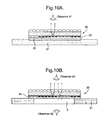
- Figures 10a and 10b show two schematic figures, illustrating how the lens based moiré system would operate in reflection only mode and in both reflection and transmission respectively.
- Figure 10a shows the reflection only scenario where the device 30 having a similar structure to that of Figure 10 is either applied onto a substantially opaque substrate 31 or partially embedded into an opaque substrate (e.g. a windowed thread) via an adhesive layer 32.
- the synthetically magnified image viewed by the observer is ultimately derived from light that has been back scattered or reflected from the micro image arrays 10, 11 and the medium that acts as a background to the micro -image array.
- the greater the reflective contrast between the micro image arrays and the surrounding back ground medium the greater the visual contrast of the synthetically magnified images.
- the colour or reflective properties of the substrate 31 are non optimal - for example the substrate may be of low reflectivity or a similar colour to one of the micro image arrays.
- an optional mask coat layer 33 located between the micro print interface and the adhesive layer 32 bonding to the device to the substrate 31.
- the mask layer 33 will typically contain a reflective opacifying pigment such as, but not limited to, titanium dioxide particles in a resin binder.
- the colour of this layer could be simply white or a colorant could be added to ensure that this mask layer or background reflecting layer exhibits a desired hue which contrasts with one or both micro image arrays.
- the mask coat and one of the micro image arrays have overtly the same colour, however one or other entity has been provided with a metameric property. Consequently under normal viewing the relevant micro image array is only weakly discerned (if at all) against the background colour of the opaque mask - however when viewed under a metameric filter said micro image array or more pertinently its synthetically magnified image becomes strongly evident.
- the mask coat may be provided with a fluorescent additive such that when viewed under a fluorescent light the mask coat provides a fluorescent background against which the absorbing micro image arrays form black synthetically magnified images.
- the mask coat may also function as a durability enhancing layer.
- metameric inks examples are provided in GB1407065 .
- the first microimage array 10 of "5"'s could be printed in a first metameric ink and the background array 11 of stars in a second metameric ink where the metameric properties of the inks are such that they appear to be of an identical colour when viewed in daylight, but when viewed in filtered light, the two inks will appear to have different reflective colours.
- Figure 10b shows the scenario where the device 30 is applied at least partially over a transparent aperture 3 within the substrate 31. It is well known to incorporate security devices into transparent apertures within secure documents (see below). In this case the synthetically magnified image may be viewed in reflection and / or transmission through the viewing aperture 3 in the substrate 31. The observer will only see magnified image when located in position #1. As can be seen in figure 10b , the opaque mask coat is omitted so we can observe the moire magnification system in transmission. It is also a requirement that the adhesive layer 34 has good optical clarity (i.e. low scatter low absorption)
- the printed micro-images 10A, 11A are formed from an ink or colorant that is substantially opaque, then the synthetically magnified image will be coloured when viewed in reflection, but will form a high contrast essentially black image when viewed in transmission.
- a requirement for a coloured image to be viewed in transmission is that the micro images must have some degree of translucency. Light must be able to pass through the printed images and the desired colour transmitted. It should be recognised that in regions were the two arrays 10, 11 and therefore magnified images overlap we will have additive colour mixing. For example if the two array colours are red and blue then in areas of overlap the image will be magenta.
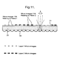
- the security device could be fabricated as a mirror-based moire device as shown in Figure 11 .
- the spherical microlens array 22 is replaced by a spherical or aspheric concave mirror array 40 formed on one surface of the transparent polymer substrate 20.
- the other surface is provided with printed microimage arrays 10, 11 as before.
- the focal length of a concave mirror is equal to half its radius of curvature R and therefore can have a limiting minimum value approaching one quarter of the mirror base diameter.
- the focal length and F number of a mirror can be one quarter of the value of equivalent lens (assuming typical refractive index of 1.5).
- reducing F number equates to reducing depth of focus, then in practice it will often be desirable to have a mirror base diameter much less than 2R.
- This structure is intended for viewing only in reflection mode and thus is most relevant for application onto opaque substrates (strip & patch) or partially embedding into opaque substrates (windowed thread).
- the printed micro images must be coincident with the focal plane of the mirrors to a precision determined by the depth of focus or field of the mirror system.
- the plane 1 micro image array 10 must be applied to the print receptive layer 21 or substrate first, then followed by the application of the plane 2 micro image array 11. This ensures that the reflective image pertaining to first plane of micro images 1 is visualised as being in front of the second plane of micro images - the first plane of images generate a synthetically magnified image.
- the incident light has to pass through or be transmitted by the printed micro image arrays 10, 11 (i.e. spatially modulated) before being reflected back as collimated light by the mirror array, then it follows that if the print micro images are substantially opaque the synthetically magnified images will take on a blackish colour or hue against the metallic hue provided by the mirror background. For the synthetically magnified images to appear with the colour of their corresponding micro image array then it is necessary that the micro images are at least partially translucent. The more translucent the micro images the brighter the colour of the synthetic images - however at a cost of reduced image contrast relative to the background.
- the background hue or colour surrounding the synthetic images will be silver - white or achromat in appearance.
- other affordable coloured metals such as Copper or it alloys maybe be used.
- Other metals such as Silver, Gold, Platinum, Chrome, Nickel, Nickel-Chrome, Palladium, Tin etc may also be used.
- the microlens array 22 or concave mirror array 40 can be integrally moulded into the polymer substrate 20 or could be formed on the surface of the substrate 20, for example by cast-curing or the like.
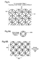
- FIG. 5 A second example is illustrated in Figures 5 and 6 . This is similar to the previous example except that the background image array 50 is defined by a series of overlapping blue circles 5 defined by means of a unit cell 52A.
- the foreground array 10 is as before.
- a further background layer is provided.
- a microlens array or concave mirror array is provided on one surface of the substrate 20 (as in Figures 10 and 11 ) and then a second, image element array 50 of blue circles 52 is printed on the opposite surface of the substrate.
- a third array 60 of green circles 62 is then printed onto the array 50 of blue circles 52.
- the unit cells 53A, 62A and parts of the arrays of these second and third layers are shown in more detail in Figure 8 .
- the pitches of the blue circles 52 and green circles 62 are selected so that the moiré magnified images appear to be at different depths (the green circles 62 below the blue circles 52) and in turn are at a different depth to the '5' icons 10A (not shown in the drawings).
- the effect of this depth difference can be seen in Figure 9 which illustrates the appearance of the security device when viewed to the left, in alignment, and to the right respectively of a normal to the security device.
- the blue and green circles appear to move relative to one another.
- the '5' icons 10A are at a different pitch from circles 52, 62 and will appear at a different depth to the circles and move relative to the circles.
- the relative pitches are chosen so that the '5' icons 10A appear, in the depth direction, between the circles 52 and 62 while in other examples the '5' icons 10A appear above both circles 52 and 62.
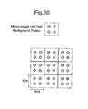
- Figures 18, 19 and 20 show further examples for the background image array.
- the array is a generic line pattern, and in Figures 19 and 20 it is an array of geometric shapes.
- Such generic patterns offer the advantage of multiredundancy if parts of the background pattern are concealed by the first image array and also there is no requirement of registration between the first image area and the background image arrays.
- Figure 12a illustrates part of apparatus for printing the image elements on the substrate.
- the apparatus shown in Figure 12 comprises an inking roll 70 coupled via a roll chain 72 to an ink reservoir 74. Ink is transferred by the roll 70 onto a print roll 76 carrying proud printing elements 78 corresponding to the microimage elements of the array concerned.
- the substrate 20 is fed between the print roll 56 and an impression roller 80 and the image elements are printed onto the substrate 20.
- a second apparatus similar to that shown in Figure 12a is provided downstream of that apparatus to print the next array of image elements.
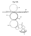
- Figure 12b illustrates alternative apparatus for printing the image elements.
- Ink is transferred by the roll 70 onto a print roll 82 carrying recessed printing elements corresponding to the microimage elements of the array concerned.
- a doctoring blade 84 contacts and removes ink or colorant off the non-recessed areas of the print roller 82.
- the substrate 20 is fed between the printing roller 82 and an impression roller 80 and the image elements are printed onto the substrate.
- a second apparatus similar to that shown in Figure 12b is provided downstream of that apparatus to print the next array of image elements.
- Microlenses or concave micromirrors are provided on the opposite surface of the substrate 20 by cast-curing, moulding or the like.
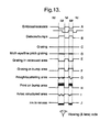
- microimage elements have been provided by printing onto the substrate. It would also be possible to provide some or all of the image elements as relief structures and examples of some of these are shown in Figures 13A-13J . In these Figures, 'IM' indicates the parts of the relief generating an image while 'NI' indicates those parts which do not generate an image.
- Figure 13A illustrates embossed or recessed image elements.
- Figure 13B illustrates debossed image elements.
- Figure 13C illustrates image elements in the form of grating structures while Figure 13D illustrates moth-eye or other fine pitch grating structures.
- Figure 13E illustrates image elements formed by gratings in recesses areas while Figure 13F illustrates gratings on debossed areas.
- Figure 13G illustrates the use of a rough embossing.
- Figure 13H illustrates the provision of print on an embossed area while Figure 13I illustrates "Aztec" shaped structures.
- Figure 13J illustrates ink filled recesses.
- the various embodiments of the device construction described above can be slit or cut into patches, foils, stripes, strips or threads for incorporation into plastic or paper substrates in accordance with known methods.
- the current invention could be incorporated into a security paper as a windowed thread.
- the security device also includes one or more other optical security features.
- a moire magnifier device 30 is formed as described with reference to Figures 2 and 10 .
- the security device also includes a number of holographic image generating structures 100.
- the holographic image structures 100 can be cast or embossed into the same resin as the microlenses but equally two different resins, one suitable for casting the microlenses and one suitable for embossing a holographic structure could be applied in register.
- the holographic structures could be embossed into a polymeric lacquer positioned on the opposite side of the polymeric layer to the microlenses.
- the holographic generating structures 100 can be in the form of holograms or DOVID image elements.
- the microlenses and the visualisation of the two magnified image arrays is located in a central horizontal band or region of the label whilst the holographic generating structures 100 are located on either side.
- the holographic generating structures 100 could be located in a central band or strip with the moiré magnifier 30 being provided in one or more regions on either side.
- moiré magnified images and the image provided by the holographic generating structures could be integrated into a single image by each providing components of a single image.
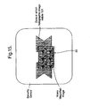
- Figure 15 illustrates an example of such an integrated design where the holographic generating structures 101 form a scroll and in the middle of the scroll the holographic structures are replaced with a moiré magnifier 30 to create a moiré magnified image in this case of moving "5"'s and stars.
- the holographic structures 100, 101 can have any conventional form and can be fully or partially metallised.
- the reflection enhancing metallised layer can be replaced with a substantially transparent inorganic high refractive index layer, such as ZnS.
- the security devices shown in the previous figures are suitable to be applied as labels to secure documents which will typically require the application of a heat or pressure sensitive adhesive to the outer surface of the device which will contact the secure document.
- an optional protective coating/varnish could be applied to the exposed outer surface of the device. The function of the protective coating/varnish is to increase the durability of the device during transfer onto the security substrate and in circulation.
- the security device is preferably prefabricated on a carrier substrate and transferred to the substrate in a subsequent working step.
- the security device can be applied to the document using an adhesive layer.
- the adhesive layer is applied either to the security device or the surface of the secure document to which the device is to be applied.
- the carrier strip can be removed leaving the security device as the exposed layer or alternatively the carrier layer can remain as part of the structure acting as an outer protective layer.
- the security device of the current invention can also be incorporated as a security strip or thread.
- Security threads are now present in many of the world's currencies as well as vouchers, passports, travellers' cheques and other documents. In many cases the thread is provided in a partially embedded or windowed fashion where the thread appears to weave in and out of the paper.
- windowed threads can be found in EP0059056 .
- EP0860298 and WO03095188 describe different approaches for the embedding of wider partially exposed threads into a paper substrate. Wide threads, typically with a width of 2-6mm, are particularly useful as the additional exposed area allows for better use of optically variable devices such as the current invention.
- the device structures shown in Figures 10 and 11 could be used as a thread by the application of a layer of transparent colourless adhesive to one or both of the outer surfaces of the device. Careful selection of the optical properties of the adhesive in contact with the microlenses is important.
- the adhesive must have a lower refractive index than the microlens material and the greater the difference in the refractive index between the microlenses and the adhesive the shorter the back focal length of the lenses and therefore the thinner the final security device.
- the security device of the current invention can be made machine readable by the introduction of detectable materials in any of the layers or by the introduction of separate machine-readable layers.
- Detectable materials that react to an external stimulus include but are not limited to fluorescent, phosphorescent, infrared absorbing, thermochromic, photochromic, magnetic, electrochromic, conductive and piezochromic materials.
- Additional optically variable materials can be included in the security device such as thin film interference elements, liquid crystal material and photonic crystal materials. Such materials may be in the form of filmic layers or as pigmented materials suitable for application by printing.
- the security device of the current invention may comprise an opaque layer.
- Figures 16 and 17 shows a further security feature in the form of a demetallised image incorporated within a security device of the current invention.
- the magnified image arrays of the device 30 are observed In the central band of the device. This provides a primary security effect due to the strong lenticular type animation.
- the structure of the feature shown in Figure 16 along section A-A is as shown in Figure 10 .
- the print receptive layer 21 has been metallised 110.
- Parts 115 of the metal layer are demetallised to define the demetallised images thus enabling the creation of demetallised indicia which can be viewed in reflective but more preferably transmitted light.
- the metallised layer forming the micromirrors may be extended beyond the micormirrors and then parts of this layer can be demetallised to define demetallised images.
- One way to produce partially metallised/demetallised films in which no metal is present in controlled and clearly defined areas, is to selectively demetallise regions using a resist and etch technique such as is described in US-B-4652015 .
- Other techniques for achieving similar effects are for example aluminium can be vacuum deposited through a mask, or aluminium can be selectively removed from a composite strip of a plastic carrier and aluminium using an excimer laser.
- the metallic regions may be alternatively provided by printing a metal effect ink having a metallic appearance such as Metalstar® inks sold by Eckart.
- a metallic layer can be used to conceal the presence of a machine readable dark magnetic layer.
- a magnetic material When a magnetic material is incorporated into the device the magnetic material can be applied in any design but common examples include the use of magnetic tramlines or the use of magnetic blocks to form a coded structure.
- Suitable magnetic materials include iron oxide pigments (Fe 2 O 3 or Fe 3 O 4 ), barium or strontium ferrites, iron, nickel, cobalt and alloys of these.
- alloys includes materials such as Nickel:Cobalt, Iron:Aluminium:Nickel:Cobalt and the like.
- Flake Nickel materials can be used; in addition Iron flake materials are suitable. Typical nickel flakes have lateral dimensions in the range 5-50 microns and a thickness less than 2 microns. Typical iron flakes have lateral dimensions in the range 10-30 microns and a thickness less than 2 microns.
- a transparent magnetic layer can be incorporated at any position within the device structure.
- Suitable transparent magnetic layers containing a distribution of particles of a magnetic material of a size and distributed in a concentration at which the magnetic layer remains transparent are described in WO03091953 and WO03091952 .
- the security device of the current invention may be incorporated in a security document such that the device is incorporated in a transparent region of the document.
- the security document may have a substrate formed from any conventional material including paper and polymer. Techniques are known in the art for forming transparent regions in each of these types of substrate.
- WO8300659 describes a polymer banknote formed from a transparent substrate comprising an opacifying coating on both sides of the substrate. The opacifying coating is omitted in localised regions on both sides of the substrate to form a transparent region.
- EP1141480 describes a method of making a transparent region in a paper substrate. Other methods for forming transparent regions in paper substrates are described in EP0723501 , EP0724519 , EP1398174 and WO03054297 .
- One or more of the microimage arrays of the present invention may be printed with inks comprising materials that respond visibly to invisible radiation.
- Luminescent materials are known to those skilled in the art to include materials having fluorescent or phosphorescent properties. It is also well known to use other materials that respond visibly to invisible radiation such as photochromic materials and thermochromic materials.
- photochromic materials and thermochromic materials For example only one of the magnified arrays might be visible in normal daylight conditions with the second magnified image becoming visible only under UV illumination. Alternatively the two magnified arrays could appear the same colour in normal daylight conditions and different colours when viewed using a filter or when viewed under UV illumination.
- the second, background array 11 of stars could be printed in an ink that is invisible under normal lighting conditions but visible under UV illumination, in this case the magnified stars will only be observed under UV illumination.
- either one or both of the first and second arrays 10, 11 could be printed in an ink that changes colour on exposure to UV radiation such that a change in colour of the magnified image is observed under UV radiation.
Landscapes
- Physics & Mathematics (AREA)
- General Physics & Mathematics (AREA)
- Engineering & Computer Science (AREA)
- Computer Security & Cryptography (AREA)
- Computer Vision & Pattern Recognition (AREA)
- Credit Cards Or The Like (AREA)
- Printing Methods (AREA)
- Optical Elements Other Than Lenses (AREA)
- Diffracting Gratings Or Hologram Optical Elements (AREA)
- Holo Graphy (AREA)
- Stereoscopic And Panoramic Photography (AREA)
- Transforming Light Signals Into Electric Signals (AREA)
- Facsimile Scanning Arrangements (AREA)
- Color Television Image Signal Generators (AREA)
Claims (22)
- Moiré-Vergrößerungsvorrichtung, umfassend ein transparentes Substrat, das Folgendes trägt:i) ein regelmäßiges Array von Mikro-Fokussierelementen auf einer ersten Oberfläche, wobei die Fokussierelemente eine Fokalebene definieren;ii) ein entsprechendes erstes Array von Mikro-Bildelementen in einer ersten Farbe, die in einer Ebene angeordnet sind, die im Wesentlichen mit der Fokalebene der Fokussierelemente zusammenfällt; undiv) ein entsprechendes zweites Array von Mikro-Bildelementen in einer zweiten Farbe, die sich von der ersten Farbe unterscheidet, und dadurch gekennzeichnet ist, dass sie in einer Ebene angeordnet sind, die im Wesentlichen mit der Fokalebene der Fokussierelemente zusammenfällt;
wobei die Teilungen der Mikro-Fokussierelemente und des ersten und zweiten Arrays von Mikro-Bildelementen und ihre relative Anordnung so gestaltet sind, dass das Array von Mikro-Fokussierelementen mit dem ersten und den zweiten Array von Mikro-Bildelementen zur Erzeugung jeweils vergrößerten Versionen der Mikro-Bildelemente eines jeden Arrays infolge des Moire-Effekts zusammenwirkt, und so, dass die vergrößerte Version des ersten Arrays von Mikro-Bildelementen gegen einen Hintergrund betrachtet wird, der von der vergrößerten Version des zweiten Arrays von Mikro-Bildelementen definiert wird, wobei die vergrößerte Version des ersten Arrays von Mikro-Bildelementen eine Bewegung relativ zum Hintergrund aufweist, wenn die Vorrichtung geneigt wird, und wobei der Teilungsversatz zwischen den Arrays so gewählt wird, dass die vergrößerte Version der Elemente des ersten Arrays oberhalb oder unterhalb der vergrößerten Version der Elemente des zweiten Arrays erscheint. - Vorrichtung nach Anspruch 1, wobei die Mikro-Fokussierelemente Mikrolinsen, wie zum Beispiel kleine sphärische Linsen, kleine Zylinderlinsen, kleine plankonvexe Linsen, kleine doppeltkonvexe Linsen, kleine Fresnel-Linsen und Fresnel-Zonenplatten umfassen.
- Vorrichtung nach Anspruch 2, wobei jede Mikrolinse einen Durchmesser im Bereich von 1 bis 100 Mikron, vorzugsweise 1 bis 50 Mikron und besonders bevorzugt 10 bis 30 Mikron hat.
- Vorrichtung nach Anspruch 1, wobei die Mikro-Fokussierelemente konkave Spiegel umfassen.
- Vorrichtung nach einem der vorhergenemdem Ansprüche, wobei die vergrößerte Version des ersten Arrays von Mikro-Bildelementen vor (oder oberhalb) der vergrößerten Version des zweiten Arrays von Mikro-Bildelementen erscheint.
- Vorrichtung nach einem der vorhergehenden Ansprüche, weiter umfassend:iv) ein entprechendes drittes Array von Mikro-Bildelementen in einer dritten Farbe, die sich von der ersten und der zweiten Farbe unterscheidet, und die in der Ebene angeordnet sind, die im Wesentlichen mit der Fokalebene der Mikro-Fokussierelemente zusammenfällt,
wobei die Teilungen der Mikro-Fokussierelemente und des dritten Arrays von Mikro-Bildelementen so gestaltet sind, dass sie bei der Erzeugung einer vergrößerten Version der Bildelemente des dritten Arrays infolge des Moire-Effekts zusammenwirken, und so, dass die vergrößerte Version des ersten Arrays von Mikro-Bildelementen gegen einen Hintergrund betrachtet wird, der von den vergrößerten Versionen des zweiten und des dritten Arrays von Mikro-Bildelementen definiert wird, wobei die vergrößerte Version des ersten Arrays von Mikro-Bildelementen eine Bewegung relativ zum Hintergrund aufweist, wenn die Vorrichtung geneigt wird. - Vorrichtung nach Anspruch 6, wobei die Teilungen des Arrays von Mikro-Fokussierelementen und des ersten, zweiten und dritten Arrays von Mikro-Bildelementen so gewählt werden, dass die vergrößerte Version des ersten Arrays von Mikro-Bildelementen zwischen den vergrößerten Versionen der Mikro-Bildelemente des zweiten und des dritten Arrays erscheint.
- Vorrichtung nach Anspruch 6, wobei Teilungen des Arrays von Mikro-Fokussierelementen und des ersten, zweiten und dritten Arrays von Mikro-Bildelementen so gewählt werden, dass die vergrößerte Version der Bildelemente des ersten Arrays oberhalb der vergrößerten Versionen der Bildelemente des zweiten und des dritten Arrays erscheint.
- Vorrichtung nach einem der vorhergehenden Ansprüche, wobei die Mikro-Bildelemente innerhalb wenigstens eines Arrays, vorzugsweise des zweiten Arrays, identisch sind.
- Vorrichtung nach einem der vorhergehenden Ansprüche, wobei die Mikro-Bildelemente eines jeden Arrays sich von den Mikro-Bildelementen eines jeden anderen Arrays unterscheiden.
- Vorrichtung nach einem der vorhergehenden Ansprüche, wobei die Mikro-Bildelemente des ersten Arrays Piktogramme wie zum Beispiel Symbole, geometrische Figuren, alphanumerische Zeichen, Logos und bildliche Darstellungen umfassen.
- Vorrichtung nach einem der vorhergehenden Ansprüche, wobei die Mikro-Bildelemente des zweiten und/oder des dritten Arrays jeweils einen allgemeinen, im typischen Fall im Wesentlichen einheitlichen Hintergrund definieren.
- Vorrichtung nach Anspruch 12, wobei der allgemeine Hintergrund von einem Linienmuster, zum Beispiel parallelen (geraden) Linien, einfachen geometrischen Figuren oder komplexen Linienstrukturen wie zum Beispiel Guilloche-Mustern definiert wird.
- Vorrichtung nach einem der vorhergehenden Ansprüche, wobei die Mikro-Bildelemente des ersten, zweiten und dritten Arrays sich weiter durch ihre Form und/oder Größe und/oder Ausrichtung voneinander unterscheiden.
- Vorrichtung nach einem der vorhergehenden Ansprüche, wobei die Mikro-Bildelemente auf das Substrat aufgedruckt sind.
- Vorrichtung nach einem der Ansprüche 1 bis 14, wobei die Mikro-Bildelemente als Gitterstrukturen, Ausnehmungen oder sonstige Reliefmuster auf dem Substrat ausgebildet sind.
- Vorrichtung nach einem der vorhergehenden Ansprüche, wobei der Abstand zwischen dem Array der Mikro-Fokussierelemente und der Ebene der Mikrobilder im Bereich von 1 bis 50 Mikron, vorzugsweise 10 bis 30 Mikron, liegt.
- Vorrichtung nach einem der vorhergehenden Ansprüche, weiter umfassend eine unterhalb des Arrays von Mikro-Bildelementen angeordnete Maskenschicht zur Bereitstellung eines weiteren Hintergrundes, gegen den die vergrößerten Versionen der Mikro-Bildelemente betrachtet werden, wobei die Maskenschicht vorzugsweise einen reflektierenden Deckfarbstoff und/oder fluoreszierendes Material enthält, und wobei die Maskenschicht und eines der Mikrobild-Arrays vorzugsweise offenkundig die selbe Farbe haben, wobei jedoch die Maskenschicht oder das Mikrobild mit einer metameren Eigenschaft versehen ist.
- Vorrichtung nach einem der vorhergehenden Ansprüche, weiter umfassend ein oder mehr optisch variable Effekterzeugungsstrukturen, die neben der Moire-Vergrößerungsvorrichtung angeordnet oder in diese integriert sind.
- Vorrichtung nach Anspruch 19, ausgebildet als Sicherheitsfaden, -etikett oder -flecken.
- Vorrichtung nach Anspruch 19 oder 20, bereitgestellt in einem transparenten Fenster eines Sicherheitsdokuments wie zum Beispiel einer Banknote, eines Personalausweises oder desgleichen.
- Artikel mit einer Vorrichtung nach einem der Ansprüche 1 bis 18, wobei der Artikel eine Banknote, ein Scheck, ein Reisepass, ein Personalausweis, ein Echtheitszertifikat, eine Fiskalmarke oder ein sonstiges Dokument von Sicherheitswert oder Personalidentität ist.
Applications Claiming Priority (2)
| Application Number | Priority Date | Filing Date | Title |
|---|---|---|---|
| GBGB1003397.5A GB201003397D0 (en) | 2010-03-01 | 2010-03-01 | Moire magnification security device |
| PCT/GB2011/050404 WO2011107788A1 (en) | 2010-03-01 | 2011-03-01 | Moire magnification device |
Publications (3)
| Publication Number | Publication Date |
|---|---|
| EP2542425A1 EP2542425A1 (de) | 2013-01-09 |
| EP2542425B1 true EP2542425B1 (de) | 2015-10-14 |
| EP2542425B2 EP2542425B2 (de) | 2019-05-08 |
Family
ID=42125795
Family Applications (5)
| Application Number | Title | Priority Date | Filing Date |
|---|---|---|---|
| EP11705996.4A Active EP2542420B2 (de) | 2010-03-01 | 2011-03-01 | Moiré-vergrösserungsvorrichtung |
| EP11705994.9A Active EP2542423B2 (de) | 2010-03-01 | 2011-03-01 | Moiré-vergrösserungsvorrichtung |
| EP11708074.7A Active EP2542425B2 (de) | 2010-03-01 | 2011-03-01 | Moiré-vergrösserungsvorrichtung |
| EP11705995.6A Active EP2542424B2 (de) | 2010-03-01 | 2011-03-01 | Moiré-vergrösserungsvorrichtung |
| EP14179415.6A Active EP2811470B1 (de) | 2010-03-01 | 2011-03-01 | Moiré-Vergrößerungsvorrichtung |
Family Applications Before (2)
| Application Number | Title | Priority Date | Filing Date |
|---|---|---|---|
| EP11705996.4A Active EP2542420B2 (de) | 2010-03-01 | 2011-03-01 | Moiré-vergrösserungsvorrichtung |
| EP11705994.9A Active EP2542423B2 (de) | 2010-03-01 | 2011-03-01 | Moiré-vergrösserungsvorrichtung |
Family Applications After (2)
| Application Number | Title | Priority Date | Filing Date |
|---|---|---|---|
| EP11705995.6A Active EP2542424B2 (de) | 2010-03-01 | 2011-03-01 | Moiré-vergrösserungsvorrichtung |
| EP14179415.6A Active EP2811470B1 (de) | 2010-03-01 | 2011-03-01 | Moiré-Vergrößerungsvorrichtung |
Country Status (11)
| Country | Link |
|---|---|
| US (4) | US10127755B2 (de) |
| EP (5) | EP2542420B2 (de) |
| JP (4) | JP6068145B2 (de) |
| CN (4) | CN102858554B (de) |
| AU (4) | AU2011222714C1 (de) |
| CA (4) | CA2791055C (de) |
| ES (3) | ES2519595T3 (de) |
| GB (1) | GB201003397D0 (de) |
| MX (4) | MX2012010058A (de) |
| PL (3) | PL2542424T3 (de) |
| WO (4) | WO2011107783A1 (de) |
Families Citing this family (135)
| Publication number | Priority date | Publication date | Assignee | Title |
|---|---|---|---|---|
| GB201003397D0 (en) | 2010-03-01 | 2010-04-14 | Rue De Int Ltd | Moire magnification security device |
| GB201003398D0 (en) * | 2010-03-01 | 2010-04-14 | Rue De Int Ltd | Optical device |
| RU2641316C9 (ru) | 2011-08-19 | 2019-03-21 | Визуал Физикс, Ллс | Опционально переводная оптическая система с уменьшенной толщиной |
| DE102011112554A1 (de) * | 2011-09-06 | 2013-03-07 | Giesecke & Devrient Gmbh | Verfahren zur Herstellung eines Sicherheitspapiers und Mikrolinsenfaden |
| AU2011101209B4 (en) * | 2011-09-20 | 2012-01-12 | Innovia Security Pty Ltd | A security element and method of producing a security element |
| GB201117523D0 (en) | 2011-10-11 | 2011-11-23 | Rue De Int Ltd | Security devices and methods of manufacture thereof |
| GB201117530D0 (en) | 2011-10-11 | 2011-11-23 | Rue De Int Ltd | Security devices |
| JP2013120354A (ja) * | 2011-12-08 | 2013-06-17 | Dainippon Printing Co Ltd | セキュリティ媒体及びそれを用いた真贋判定方法 |
| DE102012204343A1 (de) * | 2012-03-19 | 2013-09-19 | Bundesdruckerei Gmbh | Verfahren zur Herstellung eines Sicherheitsverbundkörpers und Sicherheitsverbundkörper mit zwei optisch brechenden Strukturen |
| GB201208137D0 (en) * | 2012-05-10 | 2012-06-20 | Rue De Int Ltd | Security devices and methods of manufacture therefor |
| CN102975568B (zh) * | 2012-05-30 | 2014-12-03 | 中钞特种防伪科技有限公司 | 光学防伪元件、使用该光学防伪元件的产品及其制备方法 |
| CA2881826C (en) | 2012-08-17 | 2021-03-30 | Visual Physics, Llc | A process for transferring microstructures to a final substrate |
| JP6061192B2 (ja) * | 2013-02-12 | 2017-01-18 | 独立行政法人 国立印刷局 | 立体表示形成体及びその作製方法 |
| EP2767395A1 (de) * | 2013-02-15 | 2014-08-20 | KBA-NotaSys SA | Substrate für Sicherheitspapiere und Herstellungsverfahren dafür |
| US20140265301A1 (en) * | 2013-03-15 | 2014-09-18 | 3M Innovative Properties Company | Security feature utlizing hinge material and biodata page |
| JP6410793B2 (ja) | 2013-03-15 | 2018-10-24 | ビジュアル フィジクス エルエルシー | オプティカルセキュリティデバイス |
| US9243169B2 (en) * | 2013-05-16 | 2016-01-26 | Sicpa Holding Sa | Security laminate |
| GB2514338B (en) | 2013-05-17 | 2020-06-10 | De La Rue Int Ltd | Security documents and methods of manufacture |
| CN103278870B (zh) * | 2013-05-23 | 2015-12-02 | 苏州平流层信息科技有限公司 | 利用菲涅尔透镜制作logo的方法 |
| US20140360397A1 (en) * | 2013-06-11 | 2014-12-11 | Avery Dennison Corporation | Composite image heat transfers |
| US20140367957A1 (en) * | 2013-06-13 | 2014-12-18 | Ad Lucem Corp. | Moiré magnification systems |
| US9873281B2 (en) | 2013-06-13 | 2018-01-23 | Visual Physics, Llc | Single layer image projection film |
| CN103342060B (zh) * | 2013-06-18 | 2016-01-20 | 坤达国际有限公司 | 一种立体图像印刷品及立体图像印刷工艺 |
| TW201522101A (zh) * | 2013-07-10 | 2015-06-16 | Sicpa Holding Sa | 唯一識別符及有關此唯一識別符之高安全裝置 |
| TW201502257A (zh) * | 2013-07-10 | 2015-01-16 | Sicpa Holding Sa | 包括可印碼與手性液晶聚合物層的標記 |
| GB201313363D0 (en) | 2013-07-26 | 2013-09-11 | Rue De Int Ltd | Security devices and method of manufacture |
| GB201313362D0 (en) | 2013-07-26 | 2013-09-11 | Rue De Int Ltd | Security Devices and Methods of Manufacture |
| RU2661743C2 (ru) * | 2013-09-04 | 2018-07-19 | ЛЮМЕНКО, ЭлЭлСи | Пиксельное преобразование и печать для матриц микролинз, чтобы осуществлять двухосевую активацию изображений |
| GB201317195D0 (en) | 2013-09-27 | 2013-11-13 | Rue De Int Ltd | Method of manufacturing a pattern and apparatus therefor |
| FI3078004T3 (fi) * | 2013-12-02 | 2023-04-25 | Leonhard Kurz Stiftung & Co Kg | Menetelmä turvaelementin todentamiseksi |
| MX358966B (es) * | 2013-12-03 | 2018-09-11 | Crane & Co Inc | Hoja o documento de seguridad que tiene una o más marcas de agua mejoradas. |
| WO2015119675A1 (en) * | 2014-02-10 | 2015-08-13 | Uni-Pixel Displays, Inc. | Optical alignment of multi-station flexographic printing system using moiré interference |
| EP2908341B1 (de) * | 2014-02-18 | 2018-07-11 | ams AG | Halbleitervorrichtung mit oberflächenintegriertem Fokussierelement |
| US10766292B2 (en) | 2014-03-27 | 2020-09-08 | Crane & Co., Inc. | Optical device that provides flicker-like optical effects |
| US10434812B2 (en) | 2014-03-27 | 2019-10-08 | Visual Physics, Llc | Optical device that produces flicker-like optical effects |
| EP4582263A1 (de) | 2014-07-17 | 2025-07-09 | Visual Physics, LLC | Verbessertes polymerfolienmaterial zur verwendung bei der herstellung von sicherheitsdokumenten wie banknoten |
| US20160133168A1 (en) * | 2014-11-06 | 2016-05-12 | Sung Jae Cho | Three-dimentional label having moving patterns using fine patterns and microlens |
| MX391783B (es) | 2014-09-16 | 2025-03-21 | Crane Security Tech Inc | Capa de lente de seguridad. |
| CN105620066B (zh) * | 2014-11-05 | 2018-03-20 | 中国科学院苏州纳米技术与纳米仿生研究所 | 透明微结构的制造方法 |
| US9971165B2 (en) * | 2014-12-30 | 2018-05-15 | Shenzhen China Star Optoelectronics Technology Co., Ltd. | 3D display apparatus |
| KR101721557B1 (ko) * | 2015-02-05 | 2017-03-30 | 손서경 | 위조방지를 위한 모아레 간섭무늬의 생성구조 |
| CA2976218C (en) | 2015-02-11 | 2023-02-14 | Crane & Co., Inc. | Method for the surface application of a security device to a substrate |
| CN104614790B (zh) * | 2015-03-03 | 2016-06-22 | 苏州苏大维格光电科技股份有限公司 | 平面菲涅尔透镜阵列动态放大光学膜 |
| CN107431739B (zh) * | 2015-03-17 | 2019-11-08 | 爱克发有限公司 | 安全图案生成方法 |
| GB2536877B (en) | 2015-03-23 | 2017-06-28 | De La Rue Int Ltd | Security device and method of manufacture |
| AU2015100385B4 (en) * | 2015-03-26 | 2015-07-02 | Ccl Secure Pty Ltd | An aperiodic moiré security element and method for production thereof |
| PL423060A1 (pl) * | 2015-03-26 | 2018-10-22 | Ccl Secure Pty Ltd | Element zabezpieczający wykorzystujący efekt mory tworzony przez matryce nieokresowe oraz sposób jego produkcji |
| US11029529B2 (en) | 2015-06-04 | 2021-06-08 | Stephen Y. Chou | Subwavelength structured lens having moire pattern, use and methods of making the same |
| GB2539390B (en) | 2015-06-10 | 2018-07-25 | De La Rue Int Ltd | Security devices and methods of manufacture thereof |
| DE102015008655A1 (de) * | 2015-07-03 | 2017-01-05 | Giesecke & Devrient Gmbh | Sicherheitselement mit farbfilterndem Gitter |
| GB201512118D0 (en) * | 2015-07-10 | 2015-08-19 | Rue De Int Ltd | Methods of manufacturing security documents and security devices |
| JP6808722B2 (ja) | 2015-08-27 | 2021-01-06 | クレイン セキュリティー テクノロジーズ インコーポレーテッド | 鮮明に画定された単独要素を作製し保護対象に転写するためのシングル転写プロセス又はデュアル転写プロセス |
| DE102015218829B4 (de) * | 2015-09-30 | 2018-08-16 | Bayerische Motoren Werke Aktiengesellschaft | Bilderzeugungsvorrichtung und Verfahren zur Herstellung eines Arrays bildgebender Elemente |
| JP6676917B2 (ja) * | 2015-10-07 | 2020-04-08 | 凸版印刷株式会社 | 表示体、および、表示体の真贋判定方法 |
| US10377162B2 (en) | 2015-10-19 | 2019-08-13 | Hydra Management Llc | Instant ticket redundancy via multi-chromatic indicia |
| EP4296069A3 (de) * | 2015-10-19 | 2024-03-13 | Hydragraphix LLC | Sofortige ticketredundanz über mehrfarbige kennzeichen |
| GB201520085D0 (en) | 2015-11-13 | 2015-12-30 | Rue De Int Ltd | Methods of manufacturing image element arrays for security devices |
| CN105479974B (zh) | 2015-12-01 | 2018-07-13 | 中钞特种防伪科技有限公司 | 一种光学防伪元件及使用该光学防伪元件的光学防伪产品 |
| US10189294B2 (en) | 2015-12-03 | 2019-01-29 | Lumenco, Llc | Arrays of individually oriented micro mirrors for use in imaging security devices for currency and brand authentication |
| DE102015015991A1 (de) * | 2015-12-10 | 2017-06-14 | Giesecke & Devrient Gmbh | Sicherheitselement mit Linsenrasterbild |
| CA3008163C (en) * | 2015-12-18 | 2023-03-28 | Visual Physics, Llc | Single layer image projection film |
| USD778941S1 (en) * | 2016-01-08 | 2017-02-14 | Apple Inc. | Display screen or portion thereof with graphical user interface |
| GB2549724B (en) | 2016-04-26 | 2019-12-11 | De La Rue Int Ltd | Security devices and methods of manufacturing image patterns for security devices |
| GB2550168B (en) | 2016-05-11 | 2018-07-25 | De La Rue Int Ltd | Security device and method of manufacture |
| JP6855688B2 (ja) * | 2016-05-19 | 2021-04-07 | 株式会社村田製作所 | グラビア印刷版、グラビア印刷方法および電子部品の製造方法 |
| JP6820539B2 (ja) * | 2016-06-14 | 2021-01-27 | 大日本印刷株式会社 | 変位可視化センサー |
| EP3469575A4 (de) * | 2016-06-14 | 2020-02-26 | Rolling Optics Innovation AB | Synthetisches bild und verfahren zur herstellung davon |
| JP6749633B2 (ja) * | 2016-07-11 | 2020-09-02 | 国立大学法人大阪大学 | 分光器、波長測定装置及びスペクトル測定方法 |
| GB201612290D0 (en) * | 2016-07-15 | 2016-08-31 | La Rue Int De Ltd | Methods of manufacturing a secuirty device |
| GB2557167B (en) * | 2016-09-30 | 2020-03-04 | De La Rue Int Ltd | Security devices |
| JP6256727B2 (ja) * | 2016-12-27 | 2018-01-10 | 大日本印刷株式会社 | セキュリティ媒体が配されたカード、セキュリティ媒体が配された紙 |
| EP3580067B1 (de) | 2017-02-10 | 2022-04-06 | Crane & Co., Inc. | Maschinenlesbare optische sicherheitsvorrichtung |
| CN108454265B (zh) * | 2017-02-20 | 2023-09-08 | 中钞特种防伪科技有限公司 | 防伪元件及光学防伪产品 |
| GB2562775B (en) * | 2017-05-25 | 2021-06-02 | De La Rue Int Ltd | Holographic security device and method of manufacture thereof |
| GB2562797A (en) | 2017-05-26 | 2018-11-28 | De La Rue Int Ltd | Security device and method |
| MX2019014513A (es) * | 2017-06-05 | 2020-01-27 | Crane & Co Inc | Dispositivo optico que proporciona efectos opticos de tipo parpadeo. |
| CN107271140B (zh) * | 2017-06-30 | 2019-05-21 | 大连理工大学 | 一种在实验水槽指定位置处产生极端波浪的方法 |
| CN109318618B (zh) * | 2017-07-31 | 2020-11-24 | 中钞特种防伪科技有限公司 | 光学防伪元件与防伪产品 |
| CN109551956B (zh) * | 2017-09-26 | 2021-11-26 | 昇印光电(昆山)股份有限公司 | 装饰片及电子设备盖板 |
| RS62669B1 (sr) * | 2017-09-29 | 2021-12-31 | Sicpa Holding Sa | Tanki optički sigurnosni element i metod njegovog projektovanja |
| GB2567165B (en) * | 2017-10-04 | 2020-08-26 | De La Rue Int Ltd | Improvements in security sheets comprising security elements |
| WO2019076805A1 (de) | 2017-10-20 | 2019-04-25 | Koenig & Bauer Ag | Sicherheitselement oder sicherheitsdokument |
| DE102017218802B3 (de) * | 2017-10-20 | 2018-11-15 | Koenig & Bauer Ag | Verfahren zur Herstellung eines Sicherheitselementes oder Sicherheitsdokuments |
| GB2567680B (en) | 2017-10-20 | 2022-12-21 | Pulsetech Security Ltd | Holograms |
| DE102018201871B3 (de) | 2018-02-07 | 2018-12-13 | Koenig & Bauer Ag | Anordnung aufweisend ein auf ein Substrat aufgebrachtes Druckbild und eine zumindest Teile des Druckbildes abdeckende optisch abbildende Struktur |
| DE102017218801B3 (de) * | 2017-10-20 | 2018-11-15 | Koenig & Bauer Ag | Verfahren zur Herstellung eines Sicherheitselementes oder Sicherheitsdokumentes |
| JP6478076B2 (ja) * | 2017-12-05 | 2019-03-06 | 大日本印刷株式会社 | セキュリティ媒体及びそれを用いた真贋判定方法、セキュリティ媒体が配されたカード、セキュリティ媒体が配された紙 |
| FR3075095B1 (fr) | 2017-12-14 | 2020-02-28 | Oberthur Fiduciaire Sas | Ensemble constitue d'un dispositif de transparence complexe et d'au moins un reseau de micro-images, ainsi que document de securite le comportant |
| DE102017130588A1 (de) * | 2017-12-19 | 2019-06-19 | Giesecke+Devrient Currency Technology Gmbh | Wertdokument |
| EP4163120A1 (de) * | 2018-01-03 | 2023-04-12 | Visual Physics, LLC | Mikrooptische sicherheitsvorrichtung mit interaktiven dynamischen sicherheitsmerkmalen |
| DE102018000343A1 (de) | 2018-01-17 | 2019-07-18 | Giesecke+Devrient Currency Technology Gmbh | Sicherheitselement mit Lumineszenz-Motivbereich |
| AU2018100225A4 (en) * | 2018-02-21 | 2018-03-22 | Ccl Secure Pty Ltd | Micro-imagery design integration |
| US10974536B2 (en) * | 2018-08-13 | 2021-04-13 | Crane & Co., Inc. | Lens-less micro-optic film |
| KR102817557B1 (ko) * | 2018-09-10 | 2025-06-10 | 크레인 앤 코, 인크 | 완전 마이크로-광학 보안 문서 |
| GB2578117B (en) | 2018-10-16 | 2021-06-09 | De La Rue Int Ltd | Security devices and methods for their manufacture |
| GB2578773B (en) | 2018-11-08 | 2022-03-30 | De La Rue Int Ltd | Methods of manufacturing security device components |
| GB2580069B (en) | 2018-12-20 | 2022-06-15 | De La Rue Int Ltd | Security documents and methods of manufacture thereof |
| CN109752862B (zh) * | 2019-01-10 | 2022-03-29 | 浙江理工大学 | 一种彩色图像 |
| GB2584597B (en) | 2019-03-28 | 2023-01-18 | De La Rue Int Ltd | Security device and method of manufacture thereof |
| CN111830726B (zh) * | 2019-04-19 | 2023-03-17 | 昇印光电(昆山)股份有限公司 | 3d成像薄膜 |
| EP4309913A1 (de) * | 2019-05-20 | 2024-01-24 | Crane & Co., Inc. | Eine sicherheitsvorrichtung mit nanopartikeln zur einstellung des brechungsindexes von schichten einer polymermatrix zur optimierung des mikrooptischen fokus |
| GB2589818B (en) | 2019-07-12 | 2022-12-14 | De La Rue Int Ltd | Security devices and methods of manufacture thereof |
| US11685180B2 (en) * | 2019-08-19 | 2023-06-27 | Crane & Co., Inc. | Micro-optic security device with zones of color |
| CN112505940B (zh) * | 2019-08-26 | 2023-03-24 | 昇印光电(昆山)股份有限公司 | 一种立体成像光学薄膜 |
| CN112505938B (zh) | 2019-08-26 | 2022-07-05 | 昇印光电(昆山)股份有限公司 | 立体成像膜 |
| CN118466040A (zh) | 2019-08-26 | 2024-08-09 | 昇印光电(昆山)股份有限公司 | 光学成像膜 |
| KR102153234B1 (ko) * | 2019-09-26 | 2020-09-07 | 지제이엠 주식회사 | 입체 시트 라벨 |
| GB201913913D0 (en) * | 2019-09-26 | 2019-11-13 | Optrical Ltd | Improvements in and relating to security devices |
| GB2588625B (en) | 2019-10-29 | 2022-12-14 | De La Rue Int Ltd | Method of forming a security device |
| CN112848742A (zh) * | 2019-11-27 | 2021-05-28 | 中钞特种防伪科技有限公司 | 光学防伪元件及光学防伪产品 |
| SE546623C2 (en) * | 2019-12-19 | 2025-01-02 | Ccl Secure Pty Ltd | Micro-optic device for use in a micro-optic image presentation system |
| PL3888929T3 (pl) * | 2020-03-31 | 2023-01-16 | Pentacomp Pte. Ltd. | Sposób wytwarzania dyskretyzowanej optycznej mikrostruktury zabezpieczającej na podłożu i podkładka do stosowania w tym sposobie |
| GB2594300A (en) * | 2020-04-22 | 2021-10-27 | De La Rue Int Ltd | Security documents and methods of manufacture thereof |
| JP7468137B2 (ja) * | 2020-05-19 | 2024-04-16 | Toppanホールディングス株式会社 | 表示体 |
| JP7622355B2 (ja) * | 2020-05-19 | 2025-01-28 | Toppanホールディングス株式会社 | 表示体 |
| CN111572235B (zh) * | 2020-05-21 | 2021-09-14 | 苏州大学 | 一种隐藏式立体成像薄膜 |
| US11577540B2 (en) | 2020-05-29 | 2023-02-14 | Capital One Services, Llc | Financial card with dynamic viewing angles to block card information |
| CN111554195B (zh) * | 2020-05-30 | 2022-06-14 | 京东方科技集团股份有限公司 | 柔性显示模组及其制备方法、电子设备 |
| CN113946002A (zh) * | 2020-07-17 | 2022-01-18 | 英属开曼群岛商音飞光电科技股份有限公司 | 摩尔纹成像装置 |
| EP4210965A2 (de) | 2020-09-11 | 2023-07-19 | De La Rue International Limited | Sicherheitsvorrichtungen und verfahren zur herstellung davon |
| JP7537211B2 (ja) * | 2020-09-29 | 2024-08-21 | Toppanホールディングス株式会社 | 表示体 |
| WO2022124975A1 (en) * | 2020-12-11 | 2022-06-16 | Rolling Optics Innovation Ab | Manufacturing of synthetic images with continuous animation |
| GB2592719B (en) * | 2020-12-15 | 2024-01-17 | Koenig & Bauer Banknote Solutions Sa | Methods for designing and producing a security feature |
| GB2602796B (en) | 2021-01-11 | 2023-08-23 | De La Rue Int Ltd | Optical devices and methods of manufacture thereof |
| GB202101267D0 (en) | 2021-01-29 | 2021-03-17 | De La Rue Int Ltd | Security devices and methods of manufacture thereof |
| DE102021001019A1 (de) | 2021-02-25 | 2022-08-25 | Giesecke+Devrient Currency Technology Gmbh | Sicherheitselement, Datenträger und Herstellungsverfahren |
| KR20230154070A (ko) * | 2021-03-08 | 2023-11-07 | 크레인 앤 코, 인크 | 다중-위상 아이콘 구조의 마이크로-광학 보안 디바이스 |
| EP4387849A4 (de) * | 2021-08-16 | 2025-08-13 | Crane & Co Inc | Mikrooptische sicherheitsvorrichtung mit verbesserter nassgewinnungsresistenz |
| CA3143656A1 (en) * | 2021-12-22 | 2023-06-22 | Bank Of Canada | Dynamic micro-optic security devices, their production and use |
| AU2023231419A1 (en) | 2022-03-10 | 2024-09-19 | Basf Se | Casting lacquer for screen printing |
| DE102022111098B3 (de) | 2022-05-05 | 2023-06-01 | Koenig & Bauer Ag | Druckmaschine zur Herstellung eines Sicherheitsdokuments |
| DE102022111099B3 (de) | 2022-05-05 | 2023-06-01 | Koenig & Bauer Ag | Sicherheitsdokument mit einem in seinem Substrat ausgebildeten transparenten Fenster |
| DE102022111097B3 (de) | 2022-05-05 | 2023-06-01 | Koenig & Bauer Ag | Sicherheitsdokument mit einem in seinem Substrat ausgebildeten transparenten Fenster |
| DE102022111096B3 (de) | 2022-05-05 | 2023-08-24 | Koenig & Bauer Ag | Verfahren zum Authentifizieren eines Sicherheitsdokuments |
| CN117677087B (zh) * | 2022-08-25 | 2024-10-29 | 比亚迪股份有限公司 | 光学结构、终端壳体及终端 |
Citations (10)
| Publication number | Priority date | Publication date | Assignee | Title |
|---|---|---|---|---|
| WO1994027254A1 (en) | 1993-05-11 | 1994-11-24 | De La Rue Holographics Limited | Security device |
| WO2005052650A2 (en) | 2003-11-21 | 2005-06-09 | Nanoventions, Inc. | Micro-optic security and image presentation system |
| WO2005106601A2 (en) | 2004-04-30 | 2005-11-10 | De La Rue International Limited | Arrays of microlenses and arrays of microimages on transparent security substrates |
| WO2006087138A1 (de) | 2005-02-18 | 2006-08-24 | Giesecke & Devrient Gmbh | Sicherheitselement und verfahren zu seiner herstellung |
| WO2006125224A2 (en) | 2005-05-18 | 2006-11-23 | Nanoventions Holdings, Llc. | Image presentation and micro-optic security system |
| WO2007076952A2 (de) | 2005-12-23 | 2007-07-12 | Giesecke & Devrient Gmbh | Sicherheitselement |
| US20070273143A1 (en) | 2006-05-12 | 2007-11-29 | Crane Timothy T | Micro-optic film structure that alone or together with a security document or label projects images spatially coordinated with static images and/or other projected images |
| WO2009156079A1 (de) | 2008-06-23 | 2009-12-30 | Giesecke & Devrient Gmbh | Sicherheitselement |
| WO2010015382A2 (de) | 2008-08-05 | 2010-02-11 | Giesecke & Devrient Gmbh | Sicherheitsanordnung |
| AU2011222720A1 (en) | 2010-03-01 | 2012-09-13 | De La Rue International Limited | Moire magnification device |
Family Cites Families (52)
| Publication number | Priority date | Publication date | Assignee | Title |
|---|---|---|---|---|
| US3357773A (en) * | 1964-12-31 | 1967-12-12 | Rowland Products Inc | Patterned sheet material |
| GB1407065A (en) | 1972-11-30 | 1975-09-24 | Rue Co Ltd Thomas De | Production of security documents |
| IN157644B (de) | 1981-02-19 | 1986-05-10 | Portals Ltd | |
| NZ201691A (en) | 1981-08-24 | 1985-08-30 | Commw Scient Ind Res Org | Security token made from bi-axially oriented polymeric film |
| US4652015A (en) | 1985-12-05 | 1987-03-24 | Crane Company | Security paper for currency and banknotes |
| GB2204272B (en) * | 1987-02-18 | 1991-06-19 | Metal Box Plc | Security documents |
| JP2581142B2 (ja) | 1988-03-29 | 1997-02-12 | 日本鋼管株式会社 | オーステナイト系ステンレス鋼材溶接部の耐硝酸腐食性改善方法 |
| GB9211123D0 (en) * | 1992-05-26 | 1992-07-08 | Amblehurst Ltd | Holographic device |
| DE4314380B4 (de) | 1993-05-01 | 2009-08-06 | Giesecke & Devrient Gmbh | Sicherheitspapier und Verfahren zu seiner Herstellung |
| AU5538094A (en) | 1993-05-14 | 1994-12-12 | Worldwide Notification Systems, Inc. | Apparatus and method of notifying a recipient of an unscheduled delivery |
| AT401365B (de) | 1993-10-11 | 1996-08-26 | Oesterr Nationalbank | Wertpapier |
| DE4334847A1 (de) | 1993-10-13 | 1995-04-20 | Kurz Leonhard Fa | Wertdokument mit Fenster |
| GB9612496D0 (en) | 1996-06-14 | 1996-08-14 | De La Rue Thomas & Co Ltd | Security device |
| JP3338860B2 (ja) | 1996-07-17 | 2002-10-28 | ヤマックス株式会社 | 点描画模様の装飾体 |
| GB9828770D0 (en) | 1998-12-29 | 1999-02-17 | Rue De Int Ltd | Security paper |
| JP2001026175A (ja) | 1999-07-14 | 2001-01-30 | Sony Corp | 段ボールの印刷方法及び梱包用段ボール |
| RU2261462C2 (ru) * | 1999-09-30 | 2005-09-27 | Конинклейке Филипс Электроникс Н.В. | Линзовое устройство (варианты) и множество линзовых устройств |
| US6450540B1 (en) † | 2000-11-15 | 2002-09-17 | Technology Tree Co., Ltd | Printed matter displaying various colors according to view angle |
| JP2003039583A (ja) | 2001-07-27 | 2003-02-13 | Meiwa Gravure Co Ltd | 装飾シート |
| DE10163381A1 (de) | 2001-12-21 | 2003-07-03 | Giesecke & Devrient Gmbh | Sicherheitspapier sowie Verfahren und Vorrichtung zu seiner Herstellung |
| GB0209564D0 (en) | 2002-04-25 | 2002-06-05 | Rue De Int Ltd | Improvements in substrates |
| GB2388377B (en) | 2002-05-09 | 2004-07-28 | Rue De Int Ltd | A paper sheet incorporating a security element and a method of making the same |
| EP1398174A1 (de) | 2002-09-10 | 2004-03-17 | Kba-Giori S.A. | Verstärktes Substrat für Wertpapiere |
| US7194105B2 (en) † | 2002-10-16 | 2007-03-20 | Hersch Roger D | Authentication of documents and articles by moiré patterns |
| US7429062B2 (en) * | 2002-10-30 | 2008-09-30 | Xerox Corporation | Anti-counterfeiting see-through moire security feature using frequency-varying patterns |
| JP2004317636A (ja) * | 2003-04-14 | 2004-11-11 | Sanko Sangyo Co Ltd | 被観察体 |
| JP4337114B2 (ja) | 2003-06-16 | 2009-09-30 | ヤマックス株式会社 | 虚像現出装飾体 |
| US7738175B2 (en) | 2003-11-21 | 2010-06-15 | Visual Physics, Llc | Micro-optic security and image presentation system providing modulated appearance of an in-plane image |
| DE102004044458B4 (de) * | 2004-09-15 | 2010-01-07 | Ovd Kinegram Ag | Sicherheitsdokument |
| DE102004056553B4 (de) * | 2004-11-23 | 2013-03-14 | Giesecke & Devrient Gmbh | Sicherheitsanordnung für Sicherheitsdokumente und Verfahren zum Herstellen der Sicherheitsdokumente |
| JP4590614B2 (ja) * | 2005-01-13 | 2010-12-01 | 独立行政法人 国立印刷局 | 偽造防止印刷物 |
| DE102005007749A1 (de) * | 2005-02-18 | 2006-08-31 | Giesecke & Devrient Gmbh | Sicherheitselement und Verfahren zu seiner Herstellung |
| EP1896272A1 (de) | 2005-03-29 | 2008-03-12 | Note Printing Australia Limited | Originalitätsgesicherte identifizierungsdokumente |
| JP4685101B2 (ja) † | 2005-07-12 | 2011-05-18 | グラパックジャパン株式会社 | 立体視シート構成体 |
| ES2313264T3 (es) * | 2005-09-20 | 2009-03-01 | ALCAN TECHNOLOGY & MANAGEMENT LTD. | Objeto con efecto optico. |
| DE102006029852A1 (de) † | 2006-06-27 | 2008-01-03 | Giesecke & Devrient Gmbh | Verfahren zum Aufbringen einer Mikrostruktur, Werkzeugform und Gegenstand mit Mikrostruktur |
| DE102006029850A1 (de) | 2006-06-27 | 2008-01-03 | Giesecke & Devrient Gmbh | Sicherheitselement |
| JP2008012870A (ja) | 2006-07-07 | 2008-01-24 | Grapac Japan Kk | 立体視シート構成体 |
| US20080258457A1 (en) | 2006-09-08 | 2008-10-23 | De La Rue International Limited | Method of manufacturing a security device |
| DE102007005414A1 (de) | 2007-01-30 | 2008-08-07 | Ovd Kinegram Ag | Sicherheitselement zur Sicherung von Wertdokumenten |
| BE1017460A6 (nl) | 2007-02-09 | 2008-10-07 | Leo Vermeulen Consulting Lvc | Lenticulair folie. |
| DE102007029203A1 (de) * | 2007-06-25 | 2009-01-08 | Giesecke & Devrient Gmbh | Sicherheitselement |
| DE102007029204A1 (de) | 2007-06-25 | 2009-01-08 | Giesecke & Devrient Gmbh | Sicherheitselement |
| JP5233227B2 (ja) | 2007-09-28 | 2013-07-10 | 凸版印刷株式会社 | 表示体及びラベル付き物品 |
| DE102008016795A1 (de) † | 2008-04-02 | 2009-10-08 | Giesecke & Devrient Gmbh | Verfahren zum Erzeugen einer mikrooptischen Moiré-Vergrößerungsanordnung |
| JP4953026B2 (ja) | 2008-04-23 | 2012-06-13 | ヤマックス株式会社 | 装飾体 |
| WO2009139396A1 (ja) | 2008-05-01 | 2009-11-19 | 独立行政法人 国立印刷局 | 画像形成体、真偽判別具及び真偽判別方法 |
| EP2359181A1 (de) | 2008-11-18 | 2011-08-24 | Rolling Optics AB | Zeitintegrierte integrale bildeinrichtung |
| CN101434176B (zh) * | 2008-12-25 | 2012-11-07 | 中钞特种防伪科技有限公司 | 光学防伪元件及带有该光学防伪元件的产品 |
| DE102009040975A1 (de) | 2009-09-11 | 2011-03-24 | Ovd Kinegram Ag | Mehrschichtkörper |
| FR2952194B1 (fr) † | 2009-10-30 | 2012-04-20 | Arjowiggins Security | Element de securite comportant un substrat portant une structure optique et un motif de reference, et procede associe. |
| GB0919108D0 (en) | 2009-10-30 | 2009-12-16 | Rue De Int Ltd | Security device |
-
2010
- 2010-03-01 GB GBGB1003397.5A patent/GB201003397D0/en not_active Ceased
-
2011
- 2011-03-01 US US13/580,784 patent/US10127755B2/en not_active Expired - Fee Related
- 2011-03-01 US US13/580,730 patent/US9177433B2/en not_active Expired - Fee Related
- 2011-03-01 CA CA2791055A patent/CA2791055C/en not_active Expired - Fee Related
- 2011-03-01 AU AU2011222714A patent/AU2011222714C1/en active Active
- 2011-03-01 CA CA2791161A patent/CA2791161C/en not_active Expired - Fee Related
- 2011-03-01 JP JP2012555491A patent/JP6068145B2/ja not_active Expired - Fee Related
- 2011-03-01 EP EP11705996.4A patent/EP2542420B2/de active Active
- 2011-03-01 EP EP11705994.9A patent/EP2542423B2/de active Active
- 2011-03-01 MX MX2012010058A patent/MX2012010058A/es active IP Right Grant
- 2011-03-01 US US13/580,837 patent/US8908276B2/en not_active Expired - Fee Related
- 2011-03-01 WO PCT/GB2011/050399 patent/WO2011107783A1/en not_active Ceased
- 2011-03-01 ES ES11705995.6T patent/ES2519595T3/es active Active
- 2011-03-01 WO PCT/GB2011/050407 patent/WO2011107791A1/en not_active Ceased
- 2011-03-01 CN CN201180021465.XA patent/CN102858554B/zh not_active Expired - Fee Related
- 2011-03-01 MX MX2012010057A patent/MX2012010057A/es active IP Right Grant
- 2011-03-01 ES ES14179415.6T patent/ES2575102T3/es active Active
- 2011-03-01 WO PCT/GB2011/050404 patent/WO2011107788A1/en not_active Ceased
- 2011-03-01 JP JP2012555490A patent/JP6162404B2/ja not_active Expired - Fee Related
- 2011-03-01 MX MX2012009918A patent/MX2012009918A/es active IP Right Grant
- 2011-03-01 ES ES11705996.4T patent/ES2519596T3/es active Active
- 2011-03-01 AU AU2011222715A patent/AU2011222715C1/en active Active
- 2011-03-01 PL PL11705995T patent/PL2542424T3/pl unknown
- 2011-03-01 AU AU2011222723A patent/AU2011222723C1/en active Active
- 2011-03-01 CA CA2791147A patent/CA2791147C/en not_active Expired - Fee Related
- 2011-03-01 WO PCT/GB2011/050398 patent/WO2011107782A1/en not_active Ceased
- 2011-03-01 AU AU2011222720A patent/AU2011222720C1/en active Active
- 2011-03-01 PL PL14179415.6T patent/PL2811470T3/pl unknown
- 2011-03-01 PL PL11705996T patent/PL2542420T3/pl unknown
- 2011-03-01 EP EP11708074.7A patent/EP2542425B2/de active Active
- 2011-03-01 CA CA2791160A patent/CA2791160C/en not_active Expired - Fee Related
- 2011-03-01 CN CN201180011752.2A patent/CN102844198B/zh not_active Expired - Fee Related
- 2011-03-01 US US13/580,797 patent/US9070237B2/en not_active Expired - Fee Related
- 2011-03-01 JP JP2012555489A patent/JP6006122B2/ja not_active Expired - Fee Related
- 2011-03-01 CN CN201180022006.3A patent/CN102869518B/zh not_active Expired - Fee Related
- 2011-03-01 MX MX2012009822A patent/MX2012009822A/es active IP Right Grant
- 2011-03-01 EP EP11705995.6A patent/EP2542424B2/de active Active
- 2011-03-01 JP JP2012555488A patent/JP5937522B2/ja not_active Expired - Fee Related
- 2011-03-01 EP EP14179415.6A patent/EP2811470B1/de active Active
- 2011-03-01 CN CN201180015130.7A patent/CN102869517B/zh not_active Expired - Fee Related
Patent Citations (11)
| Publication number | Priority date | Publication date | Assignee | Title |
|---|---|---|---|---|
| WO1994027254A1 (en) | 1993-05-11 | 1994-11-24 | De La Rue Holographics Limited | Security device |
| US5712731A (en) | 1993-05-11 | 1998-01-27 | Thomas De La Rue Limited | Security device for security documents such as bank notes and credit cards |
| WO2005052650A2 (en) | 2003-11-21 | 2005-06-09 | Nanoventions, Inc. | Micro-optic security and image presentation system |
| WO2005106601A2 (en) | 2004-04-30 | 2005-11-10 | De La Rue International Limited | Arrays of microlenses and arrays of microimages on transparent security substrates |
| WO2006087138A1 (de) | 2005-02-18 | 2006-08-24 | Giesecke & Devrient Gmbh | Sicherheitselement und verfahren zu seiner herstellung |
| WO2006125224A2 (en) | 2005-05-18 | 2006-11-23 | Nanoventions Holdings, Llc. | Image presentation and micro-optic security system |
| WO2007076952A2 (de) | 2005-12-23 | 2007-07-12 | Giesecke & Devrient Gmbh | Sicherheitselement |
| US20070273143A1 (en) | 2006-05-12 | 2007-11-29 | Crane Timothy T | Micro-optic film structure that alone or together with a security document or label projects images spatially coordinated with static images and/or other projected images |
| WO2009156079A1 (de) | 2008-06-23 | 2009-12-30 | Giesecke & Devrient Gmbh | Sicherheitselement |
| WO2010015382A2 (de) | 2008-08-05 | 2010-02-11 | Giesecke & Devrient Gmbh | Sicherheitsanordnung |
| AU2011222720A1 (en) | 2010-03-01 | 2012-09-13 | De La Rue International Limited | Moire magnification device |
Non-Patent Citations (4)
| Title |
|---|
| H.KAMAL ET AL.: "Properties of Moiré Magnifiers", OPTICAL ENGINEERING, vol. 37, no. ii, November 1998 (1998-11-01), pages 3007 - 3014, XP000788769 |
| M.C. HUTLEY ET AL.: "The moiré magnifier", PURE APPL. OPT., vol. 3, 1994, pages 133 - 142, XP020071153 |
| M.HUTLEY ET AL.: "The Moiré Magnifier", PURE APPL. OPT., vol. 3, 1994, pages 133 - 142, XP020071153 |
| R.STEENBLICK ET AL.: "Unison? Micro-optic Security Film", PROC. OF SPIE- IS &T ELECTRONIC IMAGING, SPIE, vol. 5310, 2004, pages 321 - 327, XP055294708 |
Also Published As
Similar Documents
| Publication | Publication Date | Title |
|---|---|---|
| EP2542425B1 (de) | Moiré-vergrösserungsvorrichtung | |
| US20130044362A1 (en) | Optical device |
Legal Events
| Date | Code | Title | Description |
|---|---|---|---|
| PUAI | Public reference made under article 153(3) epc to a published international application that has entered the european phase |
Free format text: ORIGINAL CODE: 0009012 |
|
| 17P | Request for examination filed |
Effective date: 20120903 |
|
| AK | Designated contracting states |
Kind code of ref document: A1 Designated state(s): AL AT BE BG CH CY CZ DE DK EE ES FI FR GB GR HR HU IE IS IT LI LT LU LV MC MK MT NL NO PL PT RO RS SE SI SK SM TR |
|
| DAX | Request for extension of the european patent (deleted) | ||
| REG | Reference to a national code |
Ref country code: DE Ref legal event code: R079 Ref document number: 602011020570 Country of ref document: DE Free format text: PREVIOUS MAIN CLASS: B42D0015100000 Ipc: G07D0007000000 |
|
| RIC1 | Information provided on ipc code assigned before grant |
Ipc: G07D 7/20 20060101ALI20150306BHEP Ipc: G07D 7/00 20060101AFI20150306BHEP Ipc: G02B 3/00 20060101ALI20150306BHEP Ipc: B42D 25/342 20140101ALI20150306BHEP |
|
| GRAP | Despatch of communication of intention to grant a patent |
Free format text: ORIGINAL CODE: EPIDOSNIGR1 |
|
| INTG | Intention to grant announced |
Effective date: 20150505 |
|
| GRAS | Grant fee paid |
Free format text: ORIGINAL CODE: EPIDOSNIGR3 |
|
| GRAA | (expected) grant |
Free format text: ORIGINAL CODE: 0009210 |
|
| AK | Designated contracting states |
Kind code of ref document: B1 Designated state(s): AL AT BE BG CH CY CZ DE DK EE ES FI FR GB GR HR HU IE IS IT LI LT LU LV MC MK MT NL NO PL PT RO RS SE SI SK SM TR |
|
| REG | Reference to a national code |
Ref country code: GB Ref legal event code: FG4D |
|
| REG | Reference to a national code |
Ref country code: AT Ref legal event code: REF Ref document number: 755631 Country of ref document: AT Kind code of ref document: T Effective date: 20151015 Ref country code: CH Ref legal event code: EP |
|
| REG | Reference to a national code |
Ref country code: IE Ref legal event code: FG4D |
|
| REG | Reference to a national code |
Ref country code: DE Ref legal event code: R096 Ref document number: 602011020570 Country of ref document: DE |
|
| REG | Reference to a national code |
Ref country code: SE Ref legal event code: TRGR |
|
| REG | Reference to a national code |
Ref country code: FR Ref legal event code: PLFP Year of fee payment: 6 |
|
| REG | Reference to a national code |
Ref country code: NL Ref legal event code: MP Effective date: 20151014 |
|
| REG | Reference to a national code |
Ref country code: LT Ref legal event code: MG4D |
|
| PG25 | Lapsed in a contracting state [announced via postgrant information from national office to epo] |
Ref country code: LT Free format text: LAPSE BECAUSE OF FAILURE TO SUBMIT A TRANSLATION OF THE DESCRIPTION OR TO PAY THE FEE WITHIN THE PRESCRIBED TIME-LIMIT Effective date: 20151014 Ref country code: IS Free format text: LAPSE BECAUSE OF FAILURE TO SUBMIT A TRANSLATION OF THE DESCRIPTION OR TO PAY THE FEE WITHIN THE PRESCRIBED TIME-LIMIT Effective date: 20160214 Ref country code: NL Free format text: LAPSE BECAUSE OF FAILURE TO SUBMIT A TRANSLATION OF THE DESCRIPTION OR TO PAY THE FEE WITHIN THE PRESCRIBED TIME-LIMIT Effective date: 20151014 Ref country code: HR Free format text: LAPSE BECAUSE OF FAILURE TO SUBMIT A TRANSLATION OF THE DESCRIPTION OR TO PAY THE FEE WITHIN THE PRESCRIBED TIME-LIMIT Effective date: 20151014 Ref country code: NO Free format text: LAPSE BECAUSE OF FAILURE TO SUBMIT A TRANSLATION OF THE DESCRIPTION OR TO PAY THE FEE WITHIN THE PRESCRIBED TIME-LIMIT Effective date: 20160114 Ref country code: ES Free format text: LAPSE BECAUSE OF FAILURE TO SUBMIT A TRANSLATION OF THE DESCRIPTION OR TO PAY THE FEE WITHIN THE PRESCRIBED TIME-LIMIT Effective date: 20151014 |
|
| PG25 | Lapsed in a contracting state [announced via postgrant information from national office to epo] |
Ref country code: GR Free format text: LAPSE BECAUSE OF FAILURE TO SUBMIT A TRANSLATION OF THE DESCRIPTION OR TO PAY THE FEE WITHIN THE PRESCRIBED TIME-LIMIT Effective date: 20160115 Ref country code: PL Free format text: LAPSE BECAUSE OF FAILURE TO SUBMIT A TRANSLATION OF THE DESCRIPTION OR TO PAY THE FEE WITHIN THE PRESCRIBED TIME-LIMIT Effective date: 20151014 Ref country code: LV Free format text: LAPSE BECAUSE OF FAILURE TO SUBMIT A TRANSLATION OF THE DESCRIPTION OR TO PAY THE FEE WITHIN THE PRESCRIBED TIME-LIMIT Effective date: 20151014 Ref country code: PT Free format text: LAPSE BECAUSE OF FAILURE TO SUBMIT A TRANSLATION OF THE DESCRIPTION OR TO PAY THE FEE WITHIN THE PRESCRIBED TIME-LIMIT Effective date: 20160215 Ref country code: FI Free format text: LAPSE BECAUSE OF FAILURE TO SUBMIT A TRANSLATION OF THE DESCRIPTION OR TO PAY THE FEE WITHIN THE PRESCRIBED TIME-LIMIT Effective date: 20151014 Ref country code: RS Free format text: LAPSE BECAUSE OF FAILURE TO SUBMIT A TRANSLATION OF THE DESCRIPTION OR TO PAY THE FEE WITHIN THE PRESCRIBED TIME-LIMIT Effective date: 20151014 |
|
| REG | Reference to a national code |
Ref country code: DE Ref legal event code: R026 Ref document number: 602011020570 Country of ref document: DE |
|
| PLBI | Opposition filed |
Free format text: ORIGINAL CODE: 0009260 |
|
| PLBI | Opposition filed |
Free format text: ORIGINAL CODE: 0009260 |
|
| 26 | Opposition filed |
Opponent name: GIESECKE & DEVRIENT GMBH Effective date: 20160713 |
|
| PLAX | Notice of opposition and request to file observation + time limit sent |
Free format text: ORIGINAL CODE: EPIDOSNOBS2 |
|
| 26 | Opposition filed |
Opponent name: INNOVIA SECURITY PTY LTD. Effective date: 20160714 |
|
| PG25 | Lapsed in a contracting state [announced via postgrant information from national office to epo] |
Ref country code: RO Free format text: LAPSE BECAUSE OF FAILURE TO SUBMIT A TRANSLATION OF THE DESCRIPTION OR TO PAY THE FEE WITHIN THE PRESCRIBED TIME-LIMIT Effective date: 20151014 Ref country code: DK Free format text: LAPSE BECAUSE OF FAILURE TO SUBMIT A TRANSLATION OF THE DESCRIPTION OR TO PAY THE FEE WITHIN THE PRESCRIBED TIME-LIMIT Effective date: 20151014 Ref country code: SK Free format text: LAPSE BECAUSE OF FAILURE TO SUBMIT A TRANSLATION OF THE DESCRIPTION OR TO PAY THE FEE WITHIN THE PRESCRIBED TIME-LIMIT Effective date: 20151014 Ref country code: EE Free format text: LAPSE BECAUSE OF FAILURE TO SUBMIT A TRANSLATION OF THE DESCRIPTION OR TO PAY THE FEE WITHIN THE PRESCRIBED TIME-LIMIT Effective date: 20151014 Ref country code: SM Free format text: LAPSE BECAUSE OF FAILURE TO SUBMIT A TRANSLATION OF THE DESCRIPTION OR TO PAY THE FEE WITHIN THE PRESCRIBED TIME-LIMIT Effective date: 20151014 Ref country code: BE Free format text: LAPSE BECAUSE OF NON-PAYMENT OF DUE FEES Effective date: 20160331 |
|
| PG25 | Lapsed in a contracting state [announced via postgrant information from national office to epo] |
Ref country code: MC Free format text: LAPSE BECAUSE OF FAILURE TO SUBMIT A TRANSLATION OF THE DESCRIPTION OR TO PAY THE FEE WITHIN THE PRESCRIBED TIME-LIMIT Effective date: 20151014 Ref country code: LU Free format text: LAPSE BECAUSE OF FAILURE TO SUBMIT A TRANSLATION OF THE DESCRIPTION OR TO PAY THE FEE WITHIN THE PRESCRIBED TIME-LIMIT Effective date: 20160301 |
|
| PG25 | Lapsed in a contracting state [announced via postgrant information from national office to epo] |
Ref country code: SI Free format text: LAPSE BECAUSE OF FAILURE TO SUBMIT A TRANSLATION OF THE DESCRIPTION OR TO PAY THE FEE WITHIN THE PRESCRIBED TIME-LIMIT Effective date: 20151014 |
|
| PLBB | Reply of patent proprietor to notice(s) of opposition received |
Free format text: ORIGINAL CODE: EPIDOSNOBS3 |
|
| REG | Reference to a national code |
Ref country code: IE Ref legal event code: MM4A |
|
| PG25 | Lapsed in a contracting state [announced via postgrant information from national office to epo] |
Ref country code: BE Free format text: LAPSE BECAUSE OF FAILURE TO SUBMIT A TRANSLATION OF THE DESCRIPTION OR TO PAY THE FEE WITHIN THE PRESCRIBED TIME-LIMIT Effective date: 20151014 |
|
| PG25 | Lapsed in a contracting state [announced via postgrant information from national office to epo] |
Ref country code: IE Free format text: LAPSE BECAUSE OF NON-PAYMENT OF DUE FEES Effective date: 20160301 |
|
| REG | Reference to a national code |
Ref country code: FR Ref legal event code: PLFP Year of fee payment: 7 |
|
| PG25 | Lapsed in a contracting state [announced via postgrant information from national office to epo] |
Ref country code: MT Free format text: LAPSE BECAUSE OF FAILURE TO SUBMIT A TRANSLATION OF THE DESCRIPTION OR TO PAY THE FEE WITHIN THE PRESCRIBED TIME-LIMIT Effective date: 20151014 |
|
| PLAB | Opposition data, opponent's data or that of the opponent's representative modified |
Free format text: ORIGINAL CODE: 0009299OPPO |
|
| PLAB | Opposition data, opponent's data or that of the opponent's representative modified |
Free format text: ORIGINAL CODE: 0009299OPPO |
|
| R26 | Opposition filed (corrected) |
Opponent name: GIESECKE+DEVRIENT CURRENCY TECHNOLOGY GMBH Effective date: 20160713 |
|
| R26 | Opposition filed (corrected) |
Opponent name: CCL SECURE PTY LTD Effective date: 20160714 |
|
| REG | Reference to a national code |
Ref country code: FR Ref legal event code: PLFP Year of fee payment: 8 |
|
| REG | Reference to a national code |
Ref country code: AT Ref legal event code: UEP Ref document number: 755631 Country of ref document: AT Kind code of ref document: T Effective date: 20151014 |
|
| PGFP | Annual fee paid to national office [announced via postgrant information from national office to epo] |
Ref country code: CZ Payment date: 20180214 Year of fee payment: 8 |
|
| PG25 | Lapsed in a contracting state [announced via postgrant information from national office to epo] |
Ref country code: CY Free format text: LAPSE BECAUSE OF FAILURE TO SUBMIT A TRANSLATION OF THE DESCRIPTION OR TO PAY THE FEE WITHIN THE PRESCRIBED TIME-LIMIT Effective date: 20151014 Ref country code: HU Free format text: LAPSE BECAUSE OF FAILURE TO SUBMIT A TRANSLATION OF THE DESCRIPTION OR TO PAY THE FEE WITHIN THE PRESCRIBED TIME-LIMIT; INVALID AB INITIO Effective date: 20110301 |
|
| PG25 | Lapsed in a contracting state [announced via postgrant information from national office to epo] |
Ref country code: MT Free format text: LAPSE BECAUSE OF FAILURE TO SUBMIT A TRANSLATION OF THE DESCRIPTION OR TO PAY THE FEE WITHIN THE PRESCRIBED TIME-LIMIT Effective date: 20160331 Ref country code: MK Free format text: LAPSE BECAUSE OF FAILURE TO SUBMIT A TRANSLATION OF THE DESCRIPTION OR TO PAY THE FEE WITHIN THE PRESCRIBED TIME-LIMIT Effective date: 20151014 Ref country code: TR Free format text: LAPSE BECAUSE OF FAILURE TO SUBMIT A TRANSLATION OF THE DESCRIPTION OR TO PAY THE FEE WITHIN THE PRESCRIBED TIME-LIMIT Effective date: 20151014 |
|
| PG25 | Lapsed in a contracting state [announced via postgrant information from national office to epo] |
Ref country code: BG Free format text: LAPSE BECAUSE OF FAILURE TO SUBMIT A TRANSLATION OF THE DESCRIPTION OR TO PAY THE FEE WITHIN THE PRESCRIBED TIME-LIMIT Effective date: 20151014 |
|
| APAH | Appeal reference modified |
Free format text: ORIGINAL CODE: EPIDOSCREFNO |
|
| APBM | Appeal reference recorded |
Free format text: ORIGINAL CODE: EPIDOSNREFNO |
|
| APBP | Date of receipt of notice of appeal recorded |
Free format text: ORIGINAL CODE: EPIDOSNNOA2O |
|
| PG25 | Lapsed in a contracting state [announced via postgrant information from national office to epo] |
Ref country code: AL Free format text: LAPSE BECAUSE OF FAILURE TO SUBMIT A TRANSLATION OF THE DESCRIPTION OR TO PAY THE FEE WITHIN THE PRESCRIBED TIME-LIMIT Effective date: 20151014 |
|
| APBU | Appeal procedure closed |
Free format text: ORIGINAL CODE: EPIDOSNNOA9O |
|
| PUAH | Patent maintained in amended form |
Free format text: ORIGINAL CODE: 0009272 |
|
| STAA | Information on the status of an ep patent application or granted ep patent |
Free format text: STATUS: PATENT MAINTAINED AS AMENDED |
|
| REG | Reference to a national code |
Ref country code: CH Ref legal event code: AELC |
|
| 27A | Patent maintained in amended form |
Effective date: 20190508 |
|
| AK | Designated contracting states |
Kind code of ref document: B2 Designated state(s): AL AT BE BG CH CY CZ DE DK EE ES FI FR GB GR HR HU IE IS IT LI LT LU LV MC MK MT NL NO PL PT RO RS SE SI SK SM TR |
|
| REG | Reference to a national code |
Ref country code: DE Ref legal event code: R102 Ref document number: 602011020570 Country of ref document: DE |
|
| REG | Reference to a national code |
Ref country code: SE Ref legal event code: RPEO |
|
| PG25 | Lapsed in a contracting state [announced via postgrant information from national office to epo] |
Ref country code: CZ Free format text: LAPSE BECAUSE OF FAILURE TO SUBMIT A TRANSLATION OF THE DESCRIPTION OR TO PAY THE FEE WITHIN THE PRESCRIBED TIME-LIMIT Effective date: 20151014 |
|
| PGFP | Annual fee paid to national office [announced via postgrant information from national office to epo] |
Ref country code: SE Payment date: 20200310 Year of fee payment: 10 Ref country code: IT Payment date: 20200221 Year of fee payment: 10 Ref country code: AT Payment date: 20200225 Year of fee payment: 10 |
|
| REG | Reference to a national code |
Ref country code: AT Ref legal event code: MM01 Ref document number: 755631 Country of ref document: AT Kind code of ref document: T Effective date: 20210301 |
|
| PG25 | Lapsed in a contracting state [announced via postgrant information from national office to epo] |
Ref country code: AT Free format text: LAPSE BECAUSE OF NON-PAYMENT OF DUE FEES Effective date: 20210301 Ref country code: SE Free format text: LAPSE BECAUSE OF NON-PAYMENT OF DUE FEES Effective date: 20210302 |
|
| PG25 | Lapsed in a contracting state [announced via postgrant information from national office to epo] |
Ref country code: IT Free format text: LAPSE BECAUSE OF NON-PAYMENT OF DUE FEES Effective date: 20210301 |
|
| REG | Reference to a national code |
Ref country code: AT Ref legal event code: UEP Ref document number: 755631 Country of ref document: AT Kind code of ref document: T Effective date: 20190508 |
|
| PGFP | Annual fee paid to national office [announced via postgrant information from national office to epo] |
Ref country code: CH Payment date: 20250401 Year of fee payment: 15 |
|
| PGFP | Annual fee paid to national office [announced via postgrant information from national office to epo] |
Ref country code: FR Payment date: 20251231 Year of fee payment: 16 |
|
| REG | Reference to a national code |
Ref country code: CH Ref legal event code: U11 Free format text: ST27 STATUS EVENT CODE: U-0-0-U10-U11 (AS PROVIDED BY THE NATIONAL OFFICE) Effective date: 20260401 |
|
| PGFP | Annual fee paid to national office [announced via postgrant information from national office to epo] |
Ref country code: GB Payment date: 20260106 Year of fee payment: 16 |
|
| PGFP | Annual fee paid to national office [announced via postgrant information from national office to epo] |
Ref country code: DE Payment date: 20260102 Year of fee payment: 16 |