EP2533352A1 - Farbstoffsensibilisierte solarzelle und herstellungsverfahren dafür - Google Patents
Farbstoffsensibilisierte solarzelle und herstellungsverfahren dafür Download PDFInfo
- Publication number
- EP2533352A1 EP2533352A1 EP11739506A EP11739506A EP2533352A1 EP 2533352 A1 EP2533352 A1 EP 2533352A1 EP 11739506 A EP11739506 A EP 11739506A EP 11739506 A EP11739506 A EP 11739506A EP 2533352 A1 EP2533352 A1 EP 2533352A1
- Authority
- EP
- European Patent Office
- Prior art keywords
- porous
- dye
- layer
- solar cell
- conductive metal
- Prior art date
- Legal status (The legal status is an assumption and is not a legal conclusion. Google has not performed a legal analysis and makes no representation as to the accuracy of the status listed.)
- Withdrawn
Links
Images


Classifications
-
- H—ELECTRICITY
- H01—ELECTRIC ELEMENTS
- H01G—CAPACITORS; CAPACITORS, RECTIFIERS, DETECTORS, SWITCHING DEVICES, LIGHT-SENSITIVE OR TEMPERATURE-SENSITIVE DEVICES OF THE ELECTROLYTIC TYPE
- H01G9/00—Electrolytic capacitors, rectifiers, detectors, switching devices, light-sensitive or temperature-sensitive devices; Processes of their manufacture
- H01G9/0029—Processes of manufacture
-
- H—ELECTRICITY
- H01—ELECTRIC ELEMENTS
- H01G—CAPACITORS; CAPACITORS, RECTIFIERS, DETECTORS, SWITCHING DEVICES, LIGHT-SENSITIVE OR TEMPERATURE-SENSITIVE DEVICES OF THE ELECTROLYTIC TYPE
- H01G9/00—Electrolytic capacitors, rectifiers, detectors, switching devices, light-sensitive or temperature-sensitive devices; Processes of their manufacture
- H01G9/20—Light-sensitive devices
- H01G9/2068—Panels or arrays of photoelectrochemical cells, e.g. photovoltaic modules based on photoelectrochemical cells
-
- H—ELECTRICITY
- H10—SEMICONDUCTOR DEVICES; ELECTRIC SOLID-STATE DEVICES NOT OTHERWISE PROVIDED FOR
- H10F—INORGANIC SEMICONDUCTOR DEVICES SENSITIVE TO INFRARED RADIATION, LIGHT, ELECTROMAGNETIC RADIATION OF SHORTER WAVELENGTH OR CORPUSCULAR RADIATION
- H10F10/00—Individual photovoltaic cells, e.g. solar cells
-
- H—ELECTRICITY
- H10—SEMICONDUCTOR DEVICES; ELECTRIC SOLID-STATE DEVICES NOT OTHERWISE PROVIDED FOR
- H10F—INORGANIC SEMICONDUCTOR DEVICES SENSITIVE TO INFRARED RADIATION, LIGHT, ELECTROMAGNETIC RADIATION OF SHORTER WAVELENGTH OR CORPUSCULAR RADIATION
- H10F71/00—Manufacture or treatment of devices covered by this subclass
-
- H—ELECTRICITY
- H10—SEMICONDUCTOR DEVICES; ELECTRIC SOLID-STATE DEVICES NOT OTHERWISE PROVIDED FOR
- H10F—INORGANIC SEMICONDUCTOR DEVICES SENSITIVE TO INFRARED RADIATION, LIGHT, ELECTROMAGNETIC RADIATION OF SHORTER WAVELENGTH OR CORPUSCULAR RADIATION
- H10F77/00—Constructional details of devices covered by this subclass
- H10F77/20—Electrodes
-
- H—ELECTRICITY
- H01—ELECTRIC ELEMENTS
- H01G—CAPACITORS; CAPACITORS, RECTIFIERS, DETECTORS, SWITCHING DEVICES, LIGHT-SENSITIVE OR TEMPERATURE-SENSITIVE DEVICES OF THE ELECTROLYTIC TYPE
- H01G9/00—Electrolytic capacitors, rectifiers, detectors, switching devices, light-sensitive or temperature-sensitive devices; Processes of their manufacture
- H01G9/20—Light-sensitive devices
- H01G9/2027—Light-sensitive devices comprising an oxide semiconductor electrode
- H01G9/2031—Light-sensitive devices comprising an oxide semiconductor electrode comprising titanium oxide, e.g. TiO2
-
- H—ELECTRICITY
- H01—ELECTRIC ELEMENTS
- H01G—CAPACITORS; CAPACITORS, RECTIFIERS, DETECTORS, SWITCHING DEVICES, LIGHT-SENSITIVE OR TEMPERATURE-SENSITIVE DEVICES OF THE ELECTROLYTIC TYPE
- H01G9/00—Electrolytic capacitors, rectifiers, detectors, switching devices, light-sensitive or temperature-sensitive devices; Processes of their manufacture
- H01G9/20—Light-sensitive devices
- H01G9/2059—Light-sensitive devices comprising an organic dye as the active light absorbing material, e.g. adsorbed on an electrode or dissolved in solution
-
- H—ELECTRICITY
- H10—SEMICONDUCTOR DEVICES; ELECTRIC SOLID-STATE DEVICES NOT OTHERWISE PROVIDED FOR
- H10K—ORGANIC ELECTRIC SOLID-STATE DEVICES
- H10K30/00—Organic devices sensitive to infrared radiation, light, electromagnetic radiation of shorter wavelength or corpuscular radiation
- H10K30/80—Constructional details
- H10K30/81—Electrodes
- H10K30/82—Transparent electrodes, e.g. indium tin oxide [ITO] electrodes
- H10K30/83—Transparent electrodes, e.g. indium tin oxide [ITO] electrodes comprising arrangements for extracting the current from the cell, e.g. metal finger grid systems to reduce the serial resistance of transparent electrodes
-
- Y—GENERAL TAGGING OF NEW TECHNOLOGICAL DEVELOPMENTS; GENERAL TAGGING OF CROSS-SECTIONAL TECHNOLOGIES SPANNING OVER SEVERAL SECTIONS OF THE IPC; TECHNICAL SUBJECTS COVERED BY FORMER USPC CROSS-REFERENCE ART COLLECTIONS [XRACs] AND DIGESTS
- Y02—TECHNOLOGIES OR APPLICATIONS FOR MITIGATION OR ADAPTATION AGAINST CLIMATE CHANGE
- Y02E—REDUCTION OF GREENHOUSE GAS [GHG] EMISSIONS, RELATED TO ENERGY GENERATION, TRANSMISSION OR DISTRIBUTION
- Y02E10/00—Energy generation through renewable energy sources
- Y02E10/50—Photovoltaic [PV] energy
- Y02E10/542—Dye sensitized solar cells
-
- Y—GENERAL TAGGING OF NEW TECHNOLOGICAL DEVELOPMENTS; GENERAL TAGGING OF CROSS-SECTIONAL TECHNOLOGIES SPANNING OVER SEVERAL SECTIONS OF THE IPC; TECHNICAL SUBJECTS COVERED BY FORMER USPC CROSS-REFERENCE ART COLLECTIONS [XRACs] AND DIGESTS
- Y02—TECHNOLOGIES OR APPLICATIONS FOR MITIGATION OR ADAPTATION AGAINST CLIMATE CHANGE
- Y02P—CLIMATE CHANGE MITIGATION TECHNOLOGIES IN THE PRODUCTION OR PROCESSING OF GOODS
- Y02P70/00—Climate change mitigation technologies in the production process for final industrial or consumer products
- Y02P70/50—Manufacturing or production processes characterised by the final manufactured product
Definitions
- the present invention relates to a dye-sensitized solar cell and a method for manufacturing the same.
- Dye-sensitized solar cells are called wet solar cells or Graetzel cells, and are characterized by having an electrochemical cell structure represented by an iodine solution without using a silicon semiconductor.
- dye-sensitized solar cells have a simple structure formed by baking a titanium dioxide power and the like on a transparent conductive glass plate (a transparent substrate laminated with a transparent conductive film) at a temperature of 450°C or more, for example, and arranging an iodine solution and the like as an electrolyte solution between a porous semiconductor layer, such as a titania layer in which a dye is adsorbed on the baked substrate, and a counter electrode formed from a conductive glass plate (conductive substrate).
- the power generation mechanism in a dye-sensitized solar cell is as follows.
- a dye adsorbed on a porous semiconductor layer absorbs light incident from a transparent conductive glass plate face, which is a light receiving face. This causes electrons to become excited, and the excited electrons move to the semiconductor and are led to the conductive glass. Then, the electrons that have returned to the counter electrode are led via the electrolyte solution, such as iodine, to the dye which has lost electrons, and the dye is regenerated.
- Dye-sensitized solar cells are formed from inexpensive materials and do not require extensive facilities for their production. Consequently, dye-sensitized solar cells are attracting attention as a low-cost solar cell. To reduce dye-sensitized solar cell costs even further, for example, omission of the expensive transparent conductive film is being investigated.
- One method for omitting the transparent conductive film that is being investigated is to provide wiring formed from a conductive metal on a transparent substrate that will serve as the light illumination side. However, in this case, part of the incident light is blocked by the metal wiring portion, which leads to a deterioration in the photoelectric conversion efficiency.
- a technology in which, using a wire mesh with a wire diameter of 1 ⁇ m to 10 mm as a current collector electrode that has holes, a paste of a material for a porous semiconductor layer is coated on the wire mesh, the paste is fired to form a porous semiconductor layer, and the wire mesh is arranged on a glass transparent substrate, which does not have a transparent conductive film, facing the porous semiconductor layer side (see Patent Literature 1).
- a desirable porous semiconductor layer can be obtained by firing a paste at a suitable temperature, without the paste firing temperature being limited to the heat resistance temperature of the resin of 150°C or less, for example.
- a method is also being investigated in which a current collector layer (current collector electrode) that has a thickness of about 1 to 100 ⁇ m is deposited on a semiconductor layer (porous semiconductor layer) formed on a transparent substrate such as glass while patterning using a mask and the like (e.g., see Patent Literature 2). According to this method, a desirably thin film as the current collector layer can be easily formed.
- the paste firing temperature may be limited to the heat resistance temperature of the resin of 150°C or less, for example.
- the flexed current collector layer and the counter electrode can short-circuit when the dye-sensitized solar cell is used.
- the problems to be solved are that in a technology that uses a wire mesh and the like for a current collector electrode instead of a transparent conductive film like in the above-described Patent Literature 1, the dye-sensitized solar cell producing operation is complicated and there is a limit to making the thickness of the current collector electrode a desirable thinness.
- the dye-sensitized solar cell according to the present invention is a dye-sensitized solar cell in which an electrolyte is sealed, which includes a transparent substrate, a conductive substrate that serves as a cathode, a porous semiconductor layer to which a dye is adsorbed that is arranged between the transparent substrate and the conductive substrate near or in contact with the transparent substrate, a porous conductive metal layer that serves as an anode and that is arranged in contact with the porous semiconductor layer on a side that is opposite to the transparent substrate, and a porous insulating layer that is arranged on a side of the porous conductive metal layer that is opposite to the porous semiconductor layer, characterized in that the porous conductive metal layer is deposited on the porous insulating layer, and has a thickness of 0.3 ⁇ m to 100 ⁇ m.
- the dye-sensitized solar cell according to the present invention is characterized in that preferably the porous conductive metal layer is formed from one or two or more metal materials selected from the group consisting of Ti, W, Ni, Pt, and Au.
- the dye-sensitized solar cell according to the present invention is characterized in that preferably the porous insulating layer is formed from a glass fiber molding.
- the dye-sensitized solar cell according to the present invention is preferably characterized in that both the transparent substrate and the conductive substrate are flexible substrates, and that the porous conductive metal layer and the porous insulating layer are both formed from a material having a heat resistance equal to or more than a firing temperature of the porous semiconductor layer.
- the dye-sensitized solar cell according to the present invention is characterized in that preferably the material for the porous conductive metal layer and the material for the porous insulating layer both have a melting point of 350°C or more.
- the dye-sensitized solar cell according to the present invention is characterized in that preferably the porous insulating layer has a thickness of 100 ⁇ m or less.
- a method for manufacturing a dye-sensitized solar cell according to the present invention is characterized by including:
- a method for manufacturing a dye-sensitized solar cell according to the present invention is characterized by preferably including:
- the dye-sensitized solar cell according to the present invention can be manufactured by a dye-sensitized solar cell producing operation that is less complicated than technology that uses a wire mesh and the like for a current collector electrode, because the porous conductive metal layer that serves as the anode and is deposited on the porous insulating layer and has a thickness of 0.3 ⁇ m to 100 ⁇ m. Further, there is no risk of a deterioration in the photoelectric conversion efficiency due to an increase in the diffusion resistance like when the electrolyte moves to the porous semiconductor layer via a wire mesh and the like.
- the porous conductive metal layer that has a thickness of 0.3 ⁇ m to 100 ⁇ m and the porous insulating layer are formed from materials having a heat resistance equal to or more than the firing temperature of a porous semiconductor layer, when the dye-sensitized solar cell is used in a flexed manner, the dye-sensitized solar cell according to the present invention does not short-circuit due to the porous conductive metal layer contacting the conductive substrate because the porous insulating layer is arranged between the porous conductive metal layer and the conductive substrate.
- the porous semiconductor layer is joined to the transparent substrate after the porous semiconductor layer is formed on the porous conductive metal layer and fired, problems caused by insufficient firing of the porous semiconductor layer do not occur.
- the method for manufacturing a dye-sensitized solar cell according to the present invention can suitably provide the dye-sensitized solar cell according to the present invention that has a desirably thin current collector electrode thickness, because a porous conductive metal layer that serves as the anode and that has a thickness of 0.3 ⁇ m to 100 ⁇ m is provided on the porous insulating layer by a film deposition method.
- the method for manufacturing a dye-sensitized solar cell according to the present invention can suitably provide the dye-sensitized solar cell according to the present invention that uses flexible substrates, since materials having a heat resistance equal to or more than the firing temperature of the porous semiconductor layer are used for the porous conductive metal layer that has a thickness of 0.3 ⁇ m to 100 ⁇ m and the porous insulating layer, and the porous semiconductor layer is joined to the flexible transparent substrate after the porous semiconductor layer is formed on the porous conductive metal layer and fired.
- a dye-sensitized solar cell 10 includes a transparent substrate 12, a conductive substrate 14, a porous semiconductor layer 16, a porous conductive metal layer 18, and a porous insulating layer 20.
- the dye-sensitized solar cell 10 is sealed with a sealing material (spacer) 22.
- An electrolyte 24 is sealed inside the dye-sensitized solar cell 10.
- the transparent substrate 12 is a substrate provided on the side where solar light is incident.
- the conductive substrate 14 is provided opposite the transparent substrate 12, and serves as a cathode.
- the porous semiconductor layer 16 is arranged between the transparent substrate 12 and the conductive substrate 14 near or in contact with the transparent substrate 12.
- the porous semiconductor layer 16 adsorbs a dye.
- the porous conductive metal layer 18 is a layer that has a thickness of 0.3 ⁇ m to 100 ⁇ m and is deposited on the porous insulating layer 20.
- the porous conductive metal layer 18 is arranged in contact with the porous semiconductor layer 16 on the side that is opposite to the transparent substrate 12, and serves as an anode.
- the porous insulating layer 20 is arranged facing the conductive substrate 14 on the side of the porous conductive metal layer 18 that is opposite to the porous semiconductor layer 16.
- the porous conductive metal layer 18 and the porous insulating layer 20 are both formed to be porous so that charges can favorably move based on ionic diffusion of the electrolyte between the dye adsorbed to the porous semiconductor layer 16 and the conductive substrate 14.
- the holes formed in the porous conductive metal layer 18 and the porous insulating layer 20 do not have a concave shape, but they are in communication with both faces of the layers.
- the base (the substrate that will serve as a base for forming the below-described conductive film and the like) of the transparent substrate 12 and the conductive substrate 14 may be, for example, a glass sheet, or a flexible resin sheet (a flexible transparent substrate and a flexible conductive substrate).
- Examples of the material resin used for the flexible resin sheet include PET (polyethylene terephthalate), PEN (polyethylene naphthalate), polyimide, cured acrylic resin, cured epoxy resin, cured silicone resin, various engineering plastics, cyclic polymers obtained by metathesis polymerization and the like.
- the conductive substrate 14 is provided with a conductive film on the above-described base, and a catalyst film, such as a platinum film, on the face facing the electrolyte (electrolyte solution) of the conductive film.
- the conductive film may be, for example, ITO (a tin-doped indium film) or FTO (fluorine-doped tin oxide film) or a SnO 2 film.
- the conductive substrate 14 may be provided with only a catalyst film, such as a platinum film, on the base, without being provided with a conductive film. In this case, the catalyst film acts as a conductive film.
- the thickness of the transparent substrate 12 and the conductive substrate 14 is not especially limited.
- the thickness of these substrates may be set at, for example, about 10 ⁇ m to 1 mm.
- an appropriate metal oxide such as TiO 2 , ZnO, and SnO 2 can be used.
- TiO 2 is preferred.
- the thickness of the porous semiconductor layer 16 is not especially limited. Preferably, the thickness is set at a larger-than-normal 14 ⁇ m or more. However, even if the porous semiconductor layer 16 has a normal thickness, obviously the present invention can still be suitably applied.
- One way to improve the conversion efficiency of solar light is to increase the absorption efficiency of solar light by making the thickness of the porous semiconductor layer thicker.
- the electron diffusion length exceeds the thickness dimension of the porous semiconductor layer, there is no further effect by making the porous semiconductor layer any thicker.
- drawbacks such as deterioration in the open-circuit voltage and the conversion efficiency occur.
- the electrolyte moves to the porous semiconductor layer 16 via the porous conductive metal film 18 that acts as a current collection layer, the electrons can easily move in the porous semiconductor layer 16.
- the charge-transfer resistance for the electrolyte 24 from the conductive metal film 18 increases and reverse electron transfer does not easily occur, a high conversion efficiency can be obtained even if the thickness of the porous semiconductor layer 16 is made thicker, for example, to 14 ⁇ m or more.
- the upper limit for the thickness of the porous semiconductor layer 16 can be appropriately set based on the value of the conversion efficiency to be obtained or the like, this thickness is, for example, about 40 ⁇ m.
- the particle size of the fine particles of TiO 2 to be fired is not especially limited, this particle size is preferably about 1 nm to 100 nm.
- the porous semiconductor layer 16 has a laminate structure in which the portion of the porous semiconductor layer 16 in contact with the porous conductive metal layer 18 is a comparatively coarse layer using fine particles having a particle size of about 50 ⁇ m, for example, to increase the coverage ratio of the porous semiconductor layer 16 with respect to the porous conductive metal layer 18, while the portion on the porous semiconductor layer 16 side laminated on this coarse layer is a layer having a high porosity using small fine particles having a particle size of, for example, about 10 to 30 nm.
- the porous semiconductor layer 16 is formed by firing the above-described semiconductor material at a temperature of 300°C or more, preferably at 350°C or more, and still more preferably 400°C or more.
- this temperature is set sufficiently lower than the melting point of the material for the conductive substrate 14, and is preferably a temperature of 550°C or less.
- titanium oxide titanium oxide
- porous semiconductor layer 16 by firing the above-described semiconductor material provided in a thin layer, and then repeating the firing operation while providing further thin layers to achieve the desired thickness.
- porous semiconductor layer 16 may or may not be in contact with the flexible transparent substrate 12, the gap between them is preferably as small as possible.
- the dye adsorbed to the porous semiconductor layer 16 has an absorbance in the wavelengths from 400 nm to 1,000 nm.
- this dye may include metal complexes such as a ruthenium dye and a phthalocyanine dye, and organic dyes such as a cyanine dye.
- the porous conductive metal layer 18 is formed on the porous insulating layer 20 by a film deposition method as described above.
- a film deposition method a thin film deposition method such as a coating method or sputtering can be used.
- a coating method a printing method that uses a mask is a preferred mode, because the desired holes are formed more reliably.
- the porous conductive metal layer 18 formed as a thin film on the porous insulating layer 20 is a porous substance corresponding to the holes in the porous insulating layer 20. As described above, the formed holes do not have a concave shape, but they are in communication with both faces of the layer.
- the holes may be through holes, intercommunicating holes in the porous conductive metal layer 18, or even combinations of such through holes and communicating holes.
- the heat resistance conditions of the material for the porous conductive metal layer 18 are not especially limited as long as the material has appropriate conductivity. However, when using a flexible transparent substrate as the transparent substrate 12 and a flexible conductive substrate as the conductive substrate 14, the material used for the porous conductive metal layer 18 has a heat resistance equal to or more than the firing temperature of the porous semiconductor layer 16, preferably having a melting point of 350°C or more, and more preferably a melting point of 400°C or more.
- the material for the porous conductive metal layer 18 is one or two or more metal materials selected from the group consisting of Ti, W, Ni, Pt, and Au, or a compound thereof, since this enables a conductive metal layer to be obtained that has good corrosion resistance to iodine, which is used as a charge transport ion in the electrolyte.
- the porous conductive metal layer 18 obtained by agglomerating or sintering the fine particles of such metal materials has communicating holes among the fine particles.
- the thickness of the conductive metal layer 18 is 100 ⁇ m or less, preferably 50 ⁇ m or less, and more preferably 30 ⁇ m or less, and is at least 0.3 ⁇ m or more. If the thickness of the conductive metal layer 18 greatly exceeds 100 ⁇ m, the diffusion resistance of the electrolyte passing through the conductive metal layer is too large, so that electrolyte movement may be inhibited. On the other hand, if the thickness of the conductive metal layer 18 is far less than 0.3 ⁇ m, electrical resistance increases, so that the conductive metal layer 18 is not suitable as an electrode. Thus, a porous conductive metal layer 18 that has a small thickness can be suitably and easily realized by a film deposition method on the porous insulating layer 20. Further, in this case, since the porous insulating layer 20 acts as a support, rigidity can be ensured even if the thickness of the porous conductive metal layer 18 is reduced.
- the form of the holes in the porous insulating layer 20 may be through holes that pass through the porous insulating layer 20, intercommunicating holes in the porous insulating layer 20, or even combinations of such through holes and communicating holes.
- the open area ratio may be about 30% or more, for example.
- the porous insulating layer 20 is a suitable porous substance as described above, while also having a thin thickness that is still capable of ensuring a certain amount of rigidity as a support for the porous conductive metal layer 18 that is formed as a thin film.
- the porous insulating layer 20 may be an amorphous or a crystalline substance.
- appropriate materials that can be used include an aluminum anode oxide film, an alumina fiber molding and the like. However, a glass fiber molding is preferred.
- the heat resistance conditions of the material for the porous insulating layer 20 are not especially limited.
- the material used for the porous insulating layer 20 has a heat resistance equal to or more than the firing temperature of the porous semiconductor layer 16, preferably having a melting point of 350°C or more, and more preferably a melting point of 400°C or more.
- the material for the porous insulating layer 20 has a chemical resistance against the solvent and iodine in the electrolyte.
- glass fiber molding As a material having such properties and having a sufficient open area, it is preferred to use the above-described glass fiber molding as the material for the porous insulating layer 20.
- glass fiber moldings that can be used include glass cloth woven with glass fibers, glass nonwoven cloth, which is a sheet in which glass fibers have been joined by an appropriate means, and glass paper formed in a paper-like form by straining glass fibers (some forms of nonwoven cloth are included in glass paper).
- forming the through holes that pass through the porous insulating layer 20 and the porous conductive metal layer 18 by an appropriate method such as machine processing is also a preferred mode.
- These glass fiber moldings have so-called apertures of about 1 ⁇ m to 1 mm, for example, among the intersecting fibers, and have intercommunicating holes therein.
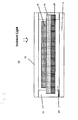
- the porous conductive metal layer 18 deposited on the glass fiber molding is formed as a thin film on the glass fibers (see Figure 4 ).
- the thickness of the porous insulating layer 20 is not especially limited as long as the thickness does not lead to an increase in the diffusion resistance of the electrolyte.
- the thickness is 100 ⁇ m or less, and more preferably 50 ⁇ m or less.
- the lower limit of the thickness is not especially set, and may be set at about 1 ⁇ m, for example.
- Examples of the electrolyte 24 include iodine, lithium ions, an ionic liquid, and t-butyl pyridine.
- the electrolyte is iodine
- a redox couple consisting of a combination of iodide ions and iodine can be used.
- the redox couple may include a suitable solvent in which the couple can dissolve.
- the method for injecting the electrolyte is not especially limited. This may be carried out by making a part of the sealing material an opening portion without being sealed, injecting the electrolyte from this opening portion, and then sealing the opening portion. Further, this can also be carried out by providing in advance an opening portion on a part of the flexible conductive substrate 14, injecting the electrolyte from this opening portion, and then sealing the opening portion.
- the dye-sensitized solar cell 10 according to the present embodiment having the above-described structure can be formed with a desirably thin current collector electrode thickness by a dye-sensitized solar cell producing operation that is less complicated than technology that uses a wire mesh and the like for a current collector electrode, because the porous conductive metal layer 18 that serves as the anode is deposited on the porous insulating layer 20. Further, since the thickness of the conductive metal layer 18 is as small as 0.3 ⁇ m to 100 ⁇ m, there is no risk of a deterioration in the photoelectric conversion efficiency due to an increase in the diffusion resistance like when the electrolyte moves to the porous semiconductor layer via a wire mesh and the like.
- the porous conductive metal layer 18 and the porous insulating layer 20 are formed from materials having a heat resistance equal to or more than the firing temperature of the porous semiconductor layer 16, when the dye-sensitized solar cell 10 is used in a flexed manner, the dye-sensitized solar cell 10 according to the present embodiment does not short-circuit due to the porous conductive metal layer 18 contacting the conductive substrate 14 because the porous insulating layer 20 is arranged between the porous conductive metal layer 18 and the conductive substrate 14.
- the porous semiconductor layer 16 is joined to the transparent substrate 12 after the porous semiconductor layer 16 is formed on the porous conductive metal layer 18 and fired, problems caused by insufficient firing of the porous semiconductor layer 16 do not occur.
- the method for manufacturing a dye-sensitized solar cell according to the first example of the present embodiment has a step of providing the porous conductive metal layer 18 that serves as an anode and has a thickness of 0.3 ⁇ m to 100 ⁇ m on the porous insulating layer 20 (step 2A, see Figures 2A and 2B ), a step of providing the conductive substrate 14 that serves as a cathode facing the porous insulating layer 20 (step 2B, see Figure 2C ), and a step of providing the porous semiconductor layer 16 in contact with the porous conductive metal layer 18 (step 2C, see Figure 2C ).
- step 2A a material having a desired open area ratio, such as a glass cloth prepared in advance, for example, is used for the porous insulating layer 20.
- through holes can also optionally be formed in the glass cloth and the like by an appropriate method such as machine processing.
- the porous conductive metal layer 18 provided on the porous insulating layer 20 is formed as a thin film that has a thickness of 0.3 ⁇ m to 100 ⁇ m by a coating method or a thin film deposition method (see Figure 2B ).
- a coating method a paste of metal particles, which are the material for the porous conductive metal layer 18, is printed on the porous insulating layer 20, heated, dried, and then fired. At this stage, an open area may be formed using a mask.
- the porous insulating layer 18 is formed by sputtering, for example. Further, at this stage, through holes can also optionally be formed in the porous insulating layer 20 and the porous conductive metal layer 18 by an appropriate method such as machine processing.
- Step 2B can be performed following step 2A, or for example, after step 2C, or as the final step performed after the transparent substrate 12 has been formed.
- the porous semiconductor layer 16 may be provided on the transparent substrate 12 or on the porous conductive metal layer 18. It is preferred to form the porous semiconductor layer 16 to a film having a desired thickness by repeating a firing operation after a thin film has been formed from a paste of fine particles of TiO 2 and the like. Further, it is preferred that the porous semiconductor layer 16 has a laminate structure in which the portion in contact with the porous conductive metal layer 18 is a comparatively coarse layer using fine particles having a relatively large particle size, while the portion on the transparent substrate 12 side laminated on this is a layer having a high porosity using fine particles having a relatively small particle size.
- the dye is adsorbed on the surface of the fine particles forming the porous semiconductor layer 16 obtained by firing.
- This adsorption method can be carried out by, for example, a so-called impregnation method in which the porous semiconductor layer 16 is formed, and then the porous insulating layer 20 on which the porous conductive metal layer 18 is provided is dipped in a dye solution to cause the dye to be chemically adsorbed to the surface of the fine particles.
- step 2C if providing the porous semiconductor layer 16 on the transparent substrate 12, the porous semiconductor layer 16 is formed by firing a paste of the material for the porous semiconductor layer 16 to be provided on the transparent substrate 12 by a coating method and the like, and then the transparent substrate 12 and the porous insulating layer 20 are joined with the porous semiconductor layer 16 side facing the porous conductive metal layer 18 side.
- the porous semiconductor layer 16 is formed by providing a paste of the material for the porous semiconductor layer 16 on the porous conductive metal layer 18 (see Figure 3C ), heating the paste and the porous insulating layer 20 on which the porous conductive metal layer 18 is provided to fire the paste, and then arranging the transparent substrate 12 opposite the porous insulating layer 20 facing the porous semiconductor layer 16 side.
- the dye-sensitized solar cell is completed by sealing each of these layers (each member) with the spacer 22 and injecting the electrolyte 24.
- the dye-sensitized solar cell according to the present embodiment can be suitably obtained having a desirably thin current collector electrode thickness.
- a dye-sensitized solar cell can be obtained having a desirably thin current collector electrode thickness by a producing operation that is less complicated than technology that uses a wire mesh and the like for a current collector electrode.
- the thickness of the porous conductive metal layer 18 is as small as 0.3 ⁇ m to 100 ⁇ m, a dye-sensitized solar cell can be obtained in which there is no risk of a deterioration in the photoelectric conversion efficiency due to an increase in the diffusion resistance like when the electrolyte moves to the porous semiconductor layer via a wire mesh and the like.
- the method for manufacturing a dye-sensitized solar cell according to the second example of the present embodiment has a step of providing the porous conductive metal layer 18 that serves as an anode and has a thickness of 0.3 ⁇ m to 100 ⁇ m on the porous insulating layer 20 (step 3A, see Figures 3A and 3B ), a step of providing a paste of the material for the porous semiconductor layer on the porous conductive metal layer 18 (step 3B, see Figure 3C ), a step of forming the porous semiconductor layer 16 by heating the paste and the porous insulating layer 20 on which the porous conductive metal layer 18 is provided to fire the paste (step 3C, see Figure 3C ), a step of arranging the flexible transparent substrate 12 opposite the porous insulating layer 20 facing the porous semiconductor layer 16 side (step 3D, see Figure 3D ), and a step of arranging the flexible conductive substrate 14 that serves as a cathode opposite the porous insulating layer 20 with the porous semiconductor layer 16 side facing out
- step 3A the porous insulating layer 20 and the porous conductive metal layer 18 are formed in the same manner as in step 2A according to the first example.
- step 3B a paste of the material for the porous semiconductor layer 16 is provided on the porous conductive metal layer 18 by an appropriate method, such as a coating method, in the same manner as in step 3B according to the first example.
- step 3C the paste is fired at a temperature of 300°C or more by heating the paste and the porous insulating layer 20 on which the porous conductive metal layer 18 is provided.
- the heating and firing temperature is not limited as long as they are lower than the melting point of the porous insulating layer 20 on which the porous conductive metal layer 18 is provided.
- the dye is adsorbed on the surface of the fine particles forming the porous semiconductor layer 16 obtained by firing.
- the flexible transparent substrate 12 formed from a resin sheet and the like is arranged opposite the porous insulating layer 20 with the porous semiconductor layer 16 side facing the flexible transparent substrate 12.
- the porous insulating layer 20, on which the porous semiconductor layer 16 and the porous conductive metal layer 18 are provided, and the flexible transparent substrate 12 are arranged so that the porous semiconductor layer 16 is in contact with or near the transparent substrate 12 (see Figure 3D ).
- the flexible conductive substrate 14 formed from a resin sheet and the like is arranged opposite the porous insulating layer 20 with the porous semiconductor layer 16 side facing outward.
- the porous insulating layer 20 and the flexible conductive substrate 14 can be appropriately arranged near each other, as long as a suitable amount of the electrolyte 24 can be injected between them.
- the dye-sensitized solar cell is completed by sealing each of these layers (each member) with the spacer 22 and injecting the electrolyte 24.
- the dye-sensitized solar cell according to the present embodiment can be suitably obtained using flexible substrates. Specifically, a dye-sensitized solar cell can be obtained that, when used in a flexed manner, does not short-circuit due to the porous conductive metal layer contacting the conductive substrate because a porous insulating layer is arranged between the porous conductive metal layer and the conductive substrate. In addition, a dye-sensitized solar cell can be obtained that is free from problems caused by insufficient firing of the porous semiconductor layer.
- Ti particles manufactured by Osaka Titanium Technologies Co., Ltd.
- an EC vehicle mainly formed from terpineol and ethyl cellulose EC-200FTD, manufactured by Nisshin Kasei Co., Ltd.
- the produced Ti particle paste was screen printed onto a 20 mm x 25 mm area of glass cloth (manufactured by Asahi Kasei E-materials Corp., void ratio of 45%) formed from glass fibers that had a thickness of 15 ⁇ m and a diameter of about 8 ⁇ m.
- a Ti particle sheet substrate was obtained by drying the paste and then firing at 400°C for 1 hour under an Ar atmosphere to form a Ti particle layer that had a thickness of about 20 ⁇ m on one side of the glass cloth.
- the Ti particle layer is formed and an SEM photograph of the Ti particle sheet substrate is illustrated in Figure 4 .
- a titania paste (trade name: Nanoxide D, manufactured by Solaronix SA) was printed on a 5 mm x 20 mm area on the Ti particle layer after firing of the Ti particle sheet substrate.
- the paste was dried, and then fired in air at 400°C for 30 minutes.
- the operation of printing and firing the titania paste on the fired titania was repeated a total of 4 times to form a titania layer that had a thickness of 12 ⁇ m on one side of the Ti particle layer.
- Ti particle sheet substrate having a titania layer was impregnated for 70 hours in a mixed solvent solution of an N719 dye (manufactured by Solaronix SA) in acetonitrile and t-butyl alcohol to adsorb the dye onto the titania surface.
- the substrate to which the dye was adsorbed was washed with a mixed solvent of acetonitrile and t-butyl alcohol.
- a laminate sheet was obtained by sandwiching and then adhering and laminating at 115°C a 60 ⁇ m-thick semi-cured resin sheet (SX1170-60, manufactured by Solaronix SA) so that a transparent resin sheet formed from 125 ⁇ m-thick polyethylene naphthalate (PEN) and the dye adsorption titania layer side of the dye-adsorbed substrate faced each other.
- the semi-cured resin sheet was arranged so as to surround but not contact the titania layer. Further, a gap of approximately 1 mm was provided in two locations to allow subsequent injection of the electrolyte.
- the transparent resin sheet On the ITO side of a transparent resin sheet provided with a transparent conductive film in which a transparent conductive film of ITO was laminated on one side of a 125 ⁇ m-thick transparent resin sheet formed from PEN, the transparent resin sheet was laminated and adhered at 115°C to the laminate sheet by sandwiching the above-described semi-cured resin sheet so that the Pt side of a sheet laminated with Pt in a thickness of about 40 nm by a sputtering technique faced the glass cloth side of the above-described laminate sheet.
- An electrolyte solution formed from iodine and LiI in an acetonitrile solvent was injected from a gap of about 1 mm, to produce a dye-sensitized solar cell that had an effective planar dimension (planar dimension of the area functioning as a cell) of 5 mm x 20 mm and a thickness of about 0.4 mm.
- the photoelectric conversion performance of the obtained dye-sensitized solar cell was checked by measuring the IV curve when simulated solar light with an intensity of 100 mW/cm 2 (using a solar simulator manufactured by Yamashita Denso Corporation) was irradiated from the transparent resin sheet side.
- the photoelectric conversion efficiency was 4.4%.
- a dye-sensitized solar cell was produced in the same manner as in Example 1, except that 50 ⁇ m-thick nonwoven cloth of glass paper (void ratio of 90%) formed from glass fibers that had a diameter of 1 to 5 ⁇ m was used instead of glass cloth.
- the photoelectric conversion efficiency of the obtained dye-sensitized solar cell was 4.1%.
- a 400 nm-thick Ti film was formed on a 20 mm x 25 mm area of a 15 ⁇ m-thick glass cloth by a sputtering technique using a mask.
- a titania paste (trade name: Nanoxide D, manufactured by Solaronix SA) was printed on a 5 mm x 20 mm area on the formed Ti film, dried, and then fired in air at 400°C for 30 minutes. A dye-sensitized solar cell was then produced in the same manner as in Example 1.
- An electrolyte solution formed from iodine and LiI in an acetonitrile solvent was injected from a gap of about 1 mm, to produce the dye-sensitized solar cell.
- the photoelectric conversion efficiency of the obtained dye-sensitized solar cell was 3.8%.
- a titania paste (trade name: Nanoxide D, manufactured by Solaronix SA) was printed, dried, and then fired in air at 150°C for 30 minutes. The operation of printing and firing the titania paste on the fired titania was repeated a total of 4 times to form a titania layer that had a thickness of 12 ⁇ m on one side of the transparent resin sheet provided with a transparent conductive film.
- the produced sheet substrate having a titania layer was impregnated for 70 hours in a mixed solvent solution of an N719 dye (manufactured by Solaronix SA) in acetonitrile and t-butyl alcohol to adsorb the dye on the titania surface.
- the substrate to which the dye was adsorbed was washed with a mixed solvent of acetonitrile and t-butyl alcohol.
- a 60 ⁇ m-thick semi-cured resin sheet (SX1170-60, manufactured by Solaronix SA) was sandwiched, laminated, and adhered at 115°C so that the titania side of a sheet substrate having a titania layer and the Pt side of a sheet formed by laminating Pt to a thickness of 40 nm by a sputtering technique on the ITO side of a transparent resin sheet provided with a transparent conductive film in which a transparent conductive film of ITO was laminated on one side of a 125 ⁇ m-thick transparent resin sheet formed from PEN faced each other.
- the semi-cured resin sheet was arranged so as to surround but not contact the titania layer. Further, a gap of approximately 1 mm was provided in two locations to allow the subsequent injection of the electrolyte.
- the photoelectric conversion efficiency of the obtained dye-sensitized solar cell was 0.1%.
- a dye-sensitized solar cell was produced in the same manner as in Example 1, except that a Ti particle layer that had a thickness of about 150 ⁇ m was formed on one side of a glass cloth instead of the Ti particle layer that had a thickness of about 20 ⁇ m.
- the photoelectric conversion efficiency of the obtained dye-sensitized solar cell was 2.1%.
- a dye-sensitized solar cell was produced in the same manner as in Example 3, except that a Ti film that had a thickness of 200 nm was produced instead of the Ti film that had a thickness of 400 nm.
- the photoelectric conversion efficiency of the obtained dye-sensitized solar cell was 0.1%.
- a dye-sensitized solar cell was produced in the same manner as in Example 1, except that a glass cloth that had a thickness of 200 ⁇ m was used instead of the glass cloth that had a thickness of 15 ⁇ m.
- the photoelectric conversion efficiency of the obtained dye-sensitized solar cell was 3.3%.
- a dye-sensitized solar cell was produced in the same manner as in Example 1, except that a glass cloth that had a thickness of 500 ⁇ m was used instead of the glass cloth that had a thickness of 15 ⁇ m.
- the photoelectric conversion efficiency of the obtained dye-sensitized solar cell was 2.8%.
Landscapes
- Engineering & Computer Science (AREA)
- Power Engineering (AREA)
- Microelectronics & Electronic Packaging (AREA)
- Chemical & Material Sciences (AREA)
- Chemical Kinetics & Catalysis (AREA)
- Electrochemistry (AREA)
- Manufacturing & Machinery (AREA)
- Hybrid Cells (AREA)
- Photovoltaic Devices (AREA)
Applications Claiming Priority (2)
| Application Number | Priority Date | Filing Date | Title |
|---|---|---|---|
| JP2010022148 | 2010-02-03 | ||
| PCT/JP2011/000001 WO2011096154A1 (ja) | 2010-02-03 | 2011-01-04 | 色素増感太陽電池およびその製造方法 |
Publications (2)
| Publication Number | Publication Date |
|---|---|
| EP2533352A1 true EP2533352A1 (de) | 2012-12-12 |
| EP2533352A4 EP2533352A4 (de) | 2015-04-22 |
Family
ID=44355175
Family Applications (1)
| Application Number | Title | Priority Date | Filing Date |
|---|---|---|---|
| EP11739506.1A Withdrawn EP2533352A4 (de) | 2010-02-03 | 2011-01-04 | Farbstoffsensibilisierte solarzelle und herstellungsverfahren dafür |
Country Status (7)
| Country | Link |
|---|---|
| US (2) | US20120305073A1 (de) |
| EP (1) | EP2533352A4 (de) |
| JP (1) | JP5678345B2 (de) |
| KR (1) | KR20120113223A (de) |
| CN (1) | CN102754273B (de) |
| TW (1) | TWI506800B (de) |
| WO (1) | WO2011096154A1 (de) |
Cited By (3)
| Publication number | Priority date | Publication date | Assignee | Title |
|---|---|---|---|---|
| EP3503141A1 (de) * | 2017-12-21 | 2019-06-26 | Exeger Operations AB | Solarzelle und verfahren zur herstellung der solarzelle |
| CN111640580A (zh) * | 2020-05-28 | 2020-09-08 | 电子科技大学中山学院 | 一种金属电极柔性染料敏化太阳能电池的结构及其制备方法 |
| EP3828948A1 (de) * | 2019-11-26 | 2021-06-02 | Exeger Operations AB | Arbeitselektrode für eine photovoltaische vorrichtung und photovoltaische vorrichtung mit der arbeitselektrode |
Families Citing this family (14)
| Publication number | Priority date | Publication date | Assignee | Title |
|---|---|---|---|---|
| JP5458271B2 (ja) * | 2008-08-29 | 2014-04-02 | 新日鉄住金化学株式会社 | 色素増感太陽電池およびその製造方法 |
| JP5498337B2 (ja) * | 2010-09-28 | 2014-05-21 | 新日鉄住金化学株式会社 | 色素増感太陽電池の立体電極の製造方法 |
| CA2850671C (en) | 2011-10-11 | 2019-08-13 | Exeger Sweden Ab | Method for manufacturing dye-sensitized solar cells and solar cells so produced |
| SE537449C2 (sv) * | 2012-04-04 | 2015-05-05 | Exeger Sweden Ab | En färgämnessensiterad solcell som innehåller ett poröst isolerande substrat samt en metod för framställning av det porösa isolerande substratet |
| SE537669C2 (sv) | 2012-04-04 | 2015-09-29 | Exeger Sweden Ab | Färgämnessensiterad solcellsmodul med seriekopplad struktursamt sätt för framställning av solcellen |
| US20150144199A1 (en) * | 2012-05-25 | 2015-05-28 | Korea Institute Of Industrial Technology | Dye-sensitized solar cell having carbon nano-web coated with graphene and method for manufacturing same |
| US10964486B2 (en) | 2013-05-17 | 2021-03-30 | Exeger Operations Ab | Dye-sensitized solar cell unit and a photovoltaic charger including the solar cell unit |
| BR112015028867B1 (pt) | 2013-05-17 | 2022-02-01 | Exeger Operations Ab | Célula solar sensibilizada por corante e método de fabricação de célula solar sensibilizada por corante |
| SE537836C2 (sv) * | 2014-02-06 | 2015-11-03 | Exeger Sweden Ab | En transparent färgämnessensibiliserad solcell samt ett sättför framställning av densamma |
| RU2649239C1 (ru) * | 2016-12-01 | 2018-03-30 | Публичное акционерное общество "Нефтяная компания "Роснефть" (ПАО "НК "Роснефть") | Сенсибилизированный красителем металлооксидный солнечный элемент |
| JP2018152411A (ja) * | 2017-03-10 | 2018-09-27 | 株式会社フジコー | バックコンタクト型ペロブスカイト光電変換素子 |
| TWI645973B (zh) * | 2017-12-15 | 2019-01-01 | 律勝科技股份有限公司 | 聚醯亞胺薄化軟性基板及其製造方法 |
| CN110247055B (zh) * | 2018-03-30 | 2020-12-04 | 宁德时代新能源科技股份有限公司 | 一种集流体,其极片和电化学装置 |
| CN110247057A (zh) * | 2018-03-30 | 2019-09-17 | 宁德时代新能源科技股份有限公司 | 一种集流体,其极片和电化学装置 |
Family Cites Families (13)
| Publication number | Priority date | Publication date | Assignee | Title |
|---|---|---|---|---|
| SE0103740D0 (sv) * | 2001-11-08 | 2001-11-08 | Forskarpatent I Vaest Ab | Photovoltaic element and production methods |
| JP2005158470A (ja) * | 2003-11-25 | 2005-06-16 | Ngk Spark Plug Co Ltd | 色素増感型太陽電池 |
| JP2005166313A (ja) * | 2003-11-28 | 2005-06-23 | Ngk Spark Plug Co Ltd | 色素増感型太陽電池 |
| JP4636802B2 (ja) * | 2004-01-09 | 2011-02-23 | 株式会社巴川製紙所 | 光電変換素子 |
| JP2005317453A (ja) * | 2004-04-30 | 2005-11-10 | Ngk Spark Plug Co Ltd | 色素増感型太陽電池及びその製造方法 |
| US7400490B2 (en) * | 2005-01-25 | 2008-07-15 | Naturalnano Research, Inc. | Ultracapacitors comprised of mineral microtubules |
| JP2007073505A (ja) | 2005-08-09 | 2007-03-22 | Sumitomo Chemical Co Ltd | 光電変換素子 |
| KR100696636B1 (ko) * | 2005-08-18 | 2007-03-19 | 삼성에스디아이 주식회사 | 염료감응 태양 전지용 염료 및 이로부터 제조된 염료감응태양 전지 |
| JP4523549B2 (ja) * | 2006-01-18 | 2010-08-11 | シャープ株式会社 | 色素増感太陽電池および色素増感太陽電池モジュール |
| JP5070704B2 (ja) | 2006-01-23 | 2012-11-14 | ソニー株式会社 | 光電変換装置 |
| WO2008004553A1 (fr) * | 2006-07-06 | 2008-01-10 | Sharp Kabushiki Kaisha | Module de cellules solaires sensible aux colorants et procédé permettant de le fabriquer |
| CN101842905B (zh) * | 2007-08-28 | 2013-01-16 | 3G太阳能光电有限公司 | 具有改善的辅助电极的光伏染料电池 |
| JP2012021212A (ja) * | 2010-07-16 | 2012-02-02 | Fujimori Kogyo Co Ltd | 電子供給体 |
-
2011
- 2011-01-04 JP JP2011552673A patent/JP5678345B2/ja not_active Expired - Fee Related
- 2011-01-04 CN CN201180007497.4A patent/CN102754273B/zh not_active Expired - Fee Related
- 2011-01-04 EP EP11739506.1A patent/EP2533352A4/de not_active Withdrawn
- 2011-01-04 US US13/574,861 patent/US20120305073A1/en not_active Abandoned
- 2011-01-04 KR KR1020127017479A patent/KR20120113223A/ko not_active Withdrawn
- 2011-01-04 WO PCT/JP2011/000001 patent/WO2011096154A1/ja not_active Ceased
- 2011-01-20 TW TW100102073A patent/TWI506800B/zh not_active IP Right Cessation
-
2013
- 2013-12-23 US US14/139,667 patent/US20140227828A1/en not_active Abandoned
Cited By (10)
| Publication number | Priority date | Publication date | Assignee | Title |
|---|---|---|---|---|
| EP3503141A1 (de) * | 2017-12-21 | 2019-06-26 | Exeger Operations AB | Solarzelle und verfahren zur herstellung der solarzelle |
| WO2019120946A1 (en) * | 2017-12-21 | 2019-06-27 | Exeger Operations Ab | A solar cell and a method for manufacturing the solar cell |
| US11270849B2 (en) | 2017-12-21 | 2022-03-08 | Exeger Operations Ab | Solar cell and a method for manufacturing the solar cell |
| US11501926B2 (en) | 2017-12-21 | 2022-11-15 | Exeger Operations Ab | Solar cell and a method for manufacturing the solar cell |
| EP3828948A1 (de) * | 2019-11-26 | 2021-06-02 | Exeger Operations AB | Arbeitselektrode für eine photovoltaische vorrichtung und photovoltaische vorrichtung mit der arbeitselektrode |
| WO2021105172A1 (en) | 2019-11-26 | 2021-06-03 | Exeger Operations Ab | A working electrode for a photovoltaic device, and a photovoltaic device including the working electrode |
| DE112020005817T5 (de) | 2019-11-26 | 2022-09-08 | Exeger Operations Ab | Arbeitselektrode für eine photovoltaische Vorrichtung und eine photovoltaische Vorrichtung mit dieser Arbeitselektrode |
| SE545641C2 (en) * | 2019-11-26 | 2023-11-21 | Exeger Operations Ab | A working electrode for a photovoltaic device, and a photovoltaic device including the working electrode |
| US11832460B2 (en) | 2019-11-26 | 2023-11-28 | Exeger Operations Ab | Working electrode for a photovoltaic device, and a photovoltaic device including the working electrode |
| CN111640580A (zh) * | 2020-05-28 | 2020-09-08 | 电子科技大学中山学院 | 一种金属电极柔性染料敏化太阳能电池的结构及其制备方法 |
Also Published As
| Publication number | Publication date |
|---|---|
| KR20120113223A (ko) | 2012-10-12 |
| TWI506800B (zh) | 2015-11-01 |
| JPWO2011096154A1 (ja) | 2013-06-10 |
| TW201128786A (en) | 2011-08-16 |
| JP5678345B2 (ja) | 2015-03-04 |
| CN102754273B (zh) | 2015-05-06 |
| EP2533352A4 (de) | 2015-04-22 |
| WO2011096154A1 (ja) | 2011-08-11 |
| CN102754273A (zh) | 2012-10-24 |
| US20120305073A1 (en) | 2012-12-06 |
| US20140227828A1 (en) | 2014-08-14 |
Similar Documents
| Publication | Publication Date | Title |
|---|---|---|
| EP2533352A1 (de) | Farbstoffsensibilisierte solarzelle und herstellungsverfahren dafür | |
| KR100947371B1 (ko) | 다파장 흡수 나노 구조 염료감응 태양전지 및 그 제조방법 | |
| JP5422645B2 (ja) | 色素増感太陽電池および色素増感太陽電池モジュール | |
| EP1933387A2 (de) | Farbstoffsensibilisierte Solarzelle | |
| EP2432069B1 (de) | Poröse elektrode, farbstoffsensibilisierte solarzelle und farbstoffsensibilisiertes solarzellenmodul | |
| WO2020141252A1 (en) | A double sided solar cell assembly | |
| CN101512828A (zh) | 染料敏化型太阳能电池组件及其制备方法 | |
| CN101675554A (zh) | 染料增感光电转换元件模块及其制造方法以及电子设备 | |
| JP2007095682A (ja) | 積層型光起電素子およびその製造方法 | |
| JP2005235725A (ja) | 色素増感型太陽電池モジュール | |
| US20070095390A1 (en) | Solar cell and manufacturing method thereof | |
| EP2479766A2 (de) | Farbstoffsensibilisierte Solarzelle und Verfahren zu ihrer Herstellung | |
| KR100854711B1 (ko) | 차단층을 포함하는 염료감응 태양전지용 광전극 및 이의제조방법 | |
| KR101140784B1 (ko) | 염료감응 태양전지 및 그 제조방법 | |
| JP5657780B2 (ja) | 光電変換素子および光電変換モジュール | |
| JP4892186B2 (ja) | 色素増感太陽電池および色素増感太陽電池モジュール | |
| JP4448478B2 (ja) | 色素増感型太陽電池モジュール | |
| KR100904684B1 (ko) | 샌드위치형 고효율 염료감응 태양전지 | |
| JP5758400B2 (ja) | 色素増感太陽電池モジュールおよびその製造方法 | |
| JP3683899B1 (ja) | 色素増感型太陽電池モジュール及びその製造方法 | |
| EP3133622B1 (de) | Element zur photoelektrischen umwandlung, farbstoffsensibilisierte solarzelle und farbstoffsensibilisiertes solarzellenmodul | |
| JP2013200960A (ja) | 光電変換素子モジュールおよびその製造方法 | |
| KR101117691B1 (ko) | 염료감응 태양전지 및 이의 제조방법 | |
| JPWO2013161557A1 (ja) | 光電変換素子モジュールおよびその製造方法 | |
| EP2613330A1 (de) | Farbstoffsensibilisierte Solarzelle |
Legal Events
| Date | Code | Title | Description |
|---|---|---|---|
| PUAI | Public reference made under article 153(3) epc to a published international application that has entered the european phase |
Free format text: ORIGINAL CODE: 0009012 |
|
| 17P | Request for examination filed |
Effective date: 20120903 |
|
| AK | Designated contracting states |
Kind code of ref document: A1 Designated state(s): AL AT BE BG CH CY CZ DE DK EE ES FI FR GB GR HR HU IE IS IT LI LT LU LV MC MK MT NL NO PL PT RO RS SE SI SK SM TR |
|
| RAP1 | Party data changed (applicant data changed or rights of an application transferred) |
Owner name: NATIONAL UNIVERSITY CORPORATION KYUSHU INSTITUTE O Owner name: NIPPON STEEL & SUMIKIN CHEMICAL CO., LTD. |
|
| DAX | Request for extension of the european patent (deleted) | ||
| RA4 | Supplementary search report drawn up and despatched (corrected) |
Effective date: 20150319 |
|
| RIC1 | Information provided on ipc code assigned before grant |
Ipc: H01M 14/00 20060101AFI20150313BHEP Ipc: H01G 9/20 20060101ALI20150313BHEP Ipc: H01L 31/04 20140101ALI20150313BHEP |
|
| STAA | Information on the status of an ep patent application or granted ep patent |
Free format text: STATUS: THE APPLICATION HAS BEEN WITHDRAWN |
|
| 18W | Application withdrawn |
Effective date: 20160205 |