EP2532034B1 - Optoelektronisches bauelement und verfahren zum herstellen eines optoelektronischen bauelements - Google Patents
Optoelektronisches bauelement und verfahren zum herstellen eines optoelektronischen bauelements Download PDFInfo
- Publication number
- EP2532034B1 EP2532034B1 EP11714529.2A EP11714529A EP2532034B1 EP 2532034 B1 EP2532034 B1 EP 2532034B1 EP 11714529 A EP11714529 A EP 11714529A EP 2532034 B1 EP2532034 B1 EP 2532034B1
- Authority
- EP
- European Patent Office
- Prior art keywords
- optoelectronic component
- radiation
- potting compound
- conversion element
- component according
- Prior art date
- Legal status (The legal status is an assumption and is not a legal conclusion. Google has not performed a legal analysis and makes no representation as to the accuracy of the status listed.)
- Active
Links
Images


Classifications
-
- H—ELECTRICITY
- H10—SEMICONDUCTOR DEVICES; ELECTRIC SOLID-STATE DEVICES NOT OTHERWISE PROVIDED FOR
- H10H—INORGANIC LIGHT-EMITTING SEMICONDUCTOR DEVICES HAVING POTENTIAL BARRIERS
- H10H20/00—Individual inorganic light-emitting semiconductor devices having potential barriers, e.g. light-emitting diodes [LED]
- H10H20/80—Constructional details
- H10H20/85—Packages
- H10H20/855—Optical field-shaping means, e.g. lenses
- H10H20/856—Reflecting means
-
- H—ELECTRICITY
- H10—SEMICONDUCTOR DEVICES; ELECTRIC SOLID-STATE DEVICES NOT OTHERWISE PROVIDED FOR
- H10H—INORGANIC LIGHT-EMITTING SEMICONDUCTOR DEVICES HAVING POTENTIAL BARRIERS
- H10H20/00—Individual inorganic light-emitting semiconductor devices having potential barriers, e.g. light-emitting diodes [LED]
- H10H20/01—Manufacture or treatment
-
- H—ELECTRICITY
- H10—SEMICONDUCTOR DEVICES; ELECTRIC SOLID-STATE DEVICES NOT OTHERWISE PROVIDED FOR
- H10H—INORGANIC LIGHT-EMITTING SEMICONDUCTOR DEVICES HAVING POTENTIAL BARRIERS
- H10H20/00—Individual inorganic light-emitting semiconductor devices having potential barriers, e.g. light-emitting diodes [LED]
- H10H20/80—Constructional details
- H10H20/84—Coatings, e.g. passivation layers or antireflective coatings
- H10H20/841—Reflective coatings, e.g. dielectric Bragg reflectors
-
- H—ELECTRICITY
- H10—SEMICONDUCTOR DEVICES; ELECTRIC SOLID-STATE DEVICES NOT OTHERWISE PROVIDED FOR
- H10H—INORGANIC LIGHT-EMITTING SEMICONDUCTOR DEVICES HAVING POTENTIAL BARRIERS
- H10H20/00—Individual inorganic light-emitting semiconductor devices having potential barriers, e.g. light-emitting diodes [LED]
- H10H20/80—Constructional details
- H10H20/85—Packages
- H10H20/8506—Containers
-
- H—ELECTRICITY
- H10—SEMICONDUCTOR DEVICES; ELECTRIC SOLID-STATE DEVICES NOT OTHERWISE PROVIDED FOR
- H10H—INORGANIC LIGHT-EMITTING SEMICONDUCTOR DEVICES HAVING POTENTIAL BARRIERS
- H10H20/00—Individual inorganic light-emitting semiconductor devices having potential barriers, e.g. light-emitting diodes [LED]
- H10H20/80—Constructional details
- H10H20/85—Packages
- H10H20/851—Wavelength conversion means
- H10H20/8516—Wavelength conversion means having a non-uniform spatial arrangement or non-uniform concentration, e.g. patterned wavelength conversion layer or wavelength conversion layer with a concentration gradient
-
- H—ELECTRICITY
- H10—SEMICONDUCTOR DEVICES; ELECTRIC SOLID-STATE DEVICES NOT OTHERWISE PROVIDED FOR
- H10H—INORGANIC LIGHT-EMITTING SEMICONDUCTOR DEVICES HAVING POTENTIAL BARRIERS
- H10H20/00—Individual inorganic light-emitting semiconductor devices having potential barriers, e.g. light-emitting diodes [LED]
- H10H20/80—Constructional details
- H10H20/85—Packages
- H10H20/852—Encapsulations
- H10H20/854—Encapsulations characterised by their material, e.g. epoxy or silicone resins
-
- H—ELECTRICITY
- H01—ELECTRIC ELEMENTS
- H01L—SEMICONDUCTOR DEVICES NOT COVERED BY CLASS H10
- H01L2924/00—Indexing scheme for arrangements or methods for connecting or disconnecting semiconductor or solid-state bodies as covered by H01L24/00
- H01L2924/0001—Technical content checked by a classifier
- H01L2924/0002—Not covered by any one of groups H01L24/00, H01L24/00 and H01L2224/00
-
- H—ELECTRICITY
- H10—SEMICONDUCTOR DEVICES; ELECTRIC SOLID-STATE DEVICES NOT OTHERWISE PROVIDED FOR
- H10H—INORGANIC LIGHT-EMITTING SEMICONDUCTOR DEVICES HAVING POTENTIAL BARRIERS
- H10H20/00—Individual inorganic light-emitting semiconductor devices having potential barriers, e.g. light-emitting diodes [LED]
- H10H20/01—Manufacture or treatment
- H10H20/036—Manufacture or treatment of packages
- H10H20/0362—Manufacture or treatment of packages of encapsulations
Definitions
- the present invention relates to an optoelectronic component and a method for producing an optoelectronic component.
- emitted radiation is coupled out depending on the desired application. It can be relevant here whether scattered light is emitted by the optoelectronic component or whether the radiation should be oriented in one direction. In many applications it is important that the radiation is emitted as focused as possible in one direction. This is important for spotlights, for example, such as a car headlight or a flashlight. Even when the emitted radiation is coupled into an optical waveguide (LWL), precise focusing of the radiation is desirable in order to avoid losses due to scattering or absorption.
- LWL optical waveguide
- an optoelectronic component with an optoelectronic semiconductor chip on a chip carrier is known.
- a radiation conversion element is arranged on the semiconductor chip.
- the side of the semiconductor chip and the radiation conversion element are surrounded by a reflective encapsulation.
- the document also discloses a method for producing such a component.
- the pamphlet JP 2009/182307 A describes a light emitting device. Light-emitting elements of the Devices are surrounded by a sealing member and a resin.
- the present invention is based on the problem of providing an optoelectronic component or a method for producing an optoelectronic component in which a well-delimited cone of light can be emitted from a coupling-out area of the optoelectronic component, so that radiation occurs in a preferred main direction.
- the optoelectronic component have an optoelectronic semiconductor chip which has a contact side and a radiation coupling-out side opposite the contact side.
- the optoelectronic component has a chip carrier to which the semiconductor chip is applied via its contact side.
- a radiation conversion element is applied to the radiation coupling-out side of the semiconductor chip.
- a potting compound is applied to the chip carrier, which laterally encloses the semiconductor chip and the radiation conversion element.
- the potting compound is a reflective potting compound. It is essentially flush with an upper edge of the radiation conversion element, so that an upper side of the radiation conversion element is free of the potting compound.
- Both the semiconductor chip and the radiation conversion element are completely surrounded on the sides by the reflective potting compound. In this way, light can only leave the semiconductor chip via the top of the radiation conversion element. Otherwise, both the semiconductor chip and the radiation conversion element are laterally enclosed by the potting compound, while the chip carrier is provided at the bottom, so that scattered light from the chip carrier and the potting compound is reflected back in the semiconductor chip or in the radiation conversion element, where it is then over the top of the radiation conversion element can be decoupled. In this way, a direction of the radiation decoupling is essentially specified which runs perpendicular to the top side of the radiation conversion element. Scattered radiation goes back into the Brought radiation conversion element, and can be coupled out via the top, so that overall a high efficiency of the optoelectronic component is achieved.
- the semiconductor chip and the radiation conversion element are laterally encased by the potting compound, it is also not necessary to provide a further housing.
- the semiconductor chip and also a connection element provided on the contact side, such as an adhesive or soldering material, are already adequately protected from environmental influences, in particular from contact with the atmosphere or with air humidity, by the potting compound.
- the optoelectronic component can easily be coupled to optical elements, such as, for example, an optical waveguide, since it has a completely flat surface towards the top.
- optical elements such as, for example, an optical waveguide
- an optoelectronic component is provided which has a well-delimited transition between a coupling-out area in the form of the top of the radiation conversion element and a reflective, bordering area in the form of the potting compound, so that during operation a well-delimited light cone is emitted from a coupling-out area of the optoelectronic component.
- a coupling surface of an optical waveguide can be brought spatially very close to the luminous surface of the optoelectronic component.
- the reflective potting compound provides a lateral reflector which not only encloses the semiconductor chip but also the radiation conversion element.
- radiation is coupled out of the optoelectronic component at a limited solid angle in the direction of the normal to the surface of the radiation conversion element. Losses through Scattering in the lateral direction or due to absorption, for example on the chip carrier, is largely avoided.
- electrical contact is made with the semiconductor chip via the chip carrier.
- the semiconductor chip for example in the form of a flip chip, can have both p and n contacts on its contact side. Both contacts can thus be connected directly to the chip carrier.
- an optoelectronic component is preferably provided which has no contacts on the radiation coupling-out side, so that there is no shadowing from contact elements or electrical connections.
- the semiconductor chip is electrically contacted via its radiation coupling-out side; this is the case, for example, with a light-emitting diode which provides at least one contact, for example the n-contact, on the radiation coupling-out side.
- the electrical contact on the radiation decoupling side is in electrical contact with the chip carrier via a conductor connection, so that after the optoelectronic component has been housed, the connection contacts are only located on the chip carrier.
- the conductor connection is embedded in the potting compound, so that it is no longer necessary to provide a further housing or protective element in order to protect the conductor connection from corrosion, for example.
- the conductor connection has a bonding wire.
- a contacting method can thus be used that is already known in connection with optoelectronic components.
- a vertical extension of the bonding wire above the radiation extraction side is smaller than a height of the radiation conversion element above the radiation extraction side. This means that the bonding wire is always covered by the potting compound, since this is flush with the upper edge of the radiation conversion element. Here, too, there is no need to provide a further housing to protect the bonding wire.
- a component height of the optoelectronic component is kept low in this way. It is only determined by the heights of the chip carrier, the semiconductor chip and the radiation conversion element. A significant miniaturization of the optoelectronic component is achieved without having to resort to special techniques, such as through-hole plating, for example.
- the vertical extension of the bonding wire over the radiation coupling-out side is in the order of magnitude of 20 to 200 ⁇ m, for example 40 ⁇ m.
- the potting compound has a matrix material such as silicone or an epoxy resin.
- a matrix material such as silicone or an epoxy resin.
- silicone is particularly advantageous because silicone is easy to process and is not destroyed by the radiation emitted by the semiconductor chip.
- the potting compound has dispersed scattering particles which have the effect that the potting compound is a reflective potting compound.
- the scattering particles contain titanium dioxide.
- Other scattering particles, for example scattering particles containing aluminum oxide, are also conceivable.
- an optical element for example a lens or an optical waveguide, is on the radiation conversion element intended.
- This optical element can be applied and fastened very easily to the planar surface of the optoelectronic component.
- the potting compound is introduced by injection.
- the potting compound can be introduced by compression molding, for example. This can take place in particular in that the potting compound is introduced through an opening provided in the chip carrier.
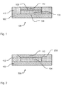
- Fig. 1 shows a schematic cross-sectional illustration through a first example of an optoelectronic component.
- the optoelectronic component 100 has a chip carrier 102.
- the chip carrier can be a ceramic carrier or a semiconductor carrier on which an optoelectronic semiconductor chip 104 is applied.
- the optoelectronic semiconductor chip 104 is a light-emitting diode or another optoelectronic element that emits or absorbs radiation.
- the optoelectronic semiconductor chip 104 can, for example, have been produced by a thin-film method. It has a contact side 106 with which it is applied to the chip carrier 102 and via which it has at least one electronic contact. It is conceivable that a further electronic contact is also connected to the chip carrier via the contact side.
- the optoelectronic semiconductor chip 104 On the side opposite the contact side 106, the optoelectronic semiconductor chip 104 has a radiation decoupling side 108. A radiation generated in the optoelectronic semiconductor chip 104 is coupled out via the radiation coupling-out side 108.
- the chip carrier 102 can, for example, have a reflective surface in the region of the contact side 106.
- a radiation conversion element 110 is applied to the radiation coupling-out side 108.
- the radiation conversion element 110 generally has a phosphorescent material in which radiation that was emitted by the optoelectronic semiconductor chip 104 is at least partially absorbed. The radiation excites a phosphorescent transition in the radiation conversion element 110. As a result, the radiation conversion element 110 emits a second radiation, the wavelength of which differs from the radiation from the optoelectronic semiconductor chip 104. In this way, the optoelectronic component 100 can emit radiation over a broad frequency spectrum.
- a potting compound 112 is applied to the chip carrier 102 and completely surrounds the optoelectronic semiconductor chip 104 and the radiation conversion element 110 at the side.
- the potting compound 112 extends up to an upper edge of the radiation conversion element 110, that is to say that it ends flush with the upper edge.
- the potting compound 112 typically has a matrix material, for example silicone or an epoxy resin. Scatter particles are dispersed in the matrix material. The scattering particles are typically titanium dioxide particles or aluminum oxide particles.
- the optoelectronic semiconductor chip 104 and the radiation conversion element 110 are laterally enclosed by the potting compound 112, scattered radiation that is emitted laterally by the semiconductor chip 104 or the radiation conversion element 110 is reflected back again and ideally reaches the radiation conversion element 110 again, from which it is coupled out via the top can be.
- radiation is only coupled out via the upper side of the radiation conversion element 110 and is in this respect sharply focused, ie it is a well-delimited transition between the coupling-out surface, which is represented by the top of the radiation conversion element 110 and the surrounding area of the potting compound 112 is achieved, so that a well-delimited light cone can be emitted from a coupling-out surface of the optoelectronic component.
- the optoelectronic component 100 has a particularly planar surface.
- the optoelectronic semiconductor chip 104 is completely enclosed by the radiation conversion element 110, the chip carrier 112 and the potting compound 112, so that no further housing has to be provided to protect the optoelectronic semiconductor chip 104.
- an optoelectronic component can thus be produced in a simple manner. It is suitable for further use, without special precautions having to be taken in order to form radiation coupling out of the electronic semiconductor chip 104 or to provide a special housing to protect the optoelectronic semiconductor chip 104.
- Fig. 2 shows a schematic illustration of a cross section through a first exemplary embodiment of an optoelectronic component according to the invention.
- the optoelectronic component 200 differs from the optoelectronic component 100 of the first example in that the radiation conversion element 110 has a particular shape.
- a stop edge 202 is provided on the radiation conversion element 110, which serves to create a boundary for lateral wetting during the production of the optoelectronic component 200 when potting with the potting compound 112, so that the potting compound 112 is flush with the top of the radiation conversion element 110.
- the radiation conversion element 110 has a cone-like, i.e. truncated pyramid-like shape, so that the stop edge 202 runs away from the surface of the optoelectronic semiconductor chip 104 and, in addition to its function as a wetting limit, can also fulfill the function of a reflector.
- the course of the stop edge 202 can be linear, as shown in the drawing. It is also conceivable that there are other courses of the stop edge 202, for example courses that are concave or convex.
- the optoelectronic component 200 shows in particular the property that a radiation path of the coupled-out radiation is focused due to the shape of the stop edge 202 and runs in the direction of the normal to the surface of the radiation conversion element 110.
- Fig. 3 shows the schematic representation of a cross section through a second example of an optoelectronic component.
- the optoelectronic component 300 differs from the optoelectronic component 100 of the first example in that a conductor connection 302 is provided, with which a contact connection is made via the radiation decoupling side 108 to the chip carrier 102.
- the conductor connection 302 is in particular a bonding wire which, in its vertical extension 304, does not rise higher than the height of the radiation conversion element above the radiation coupling-out side 108. This ensures that the conductor connection 302 is completely enclosed by the potting compound 112.
- a typical size for the vertical extension 304 is on the order of 20 to 200 ⁇ m, for example 40 ⁇ m.
- FIG. 12 shows the schematic illustration of a cross section through a third example of an optoelectronic component, wherein the optoelectronic component 400 differs from the optoelectronic component 300 of the second example differs in that an optical element 402 in the form of a lens is applied above the radiation conversion element, ie directly on its upper side. A further beam shape of the coupled-out radiation can thus take place.
- the optical element 402 as in FIG Fig. 4 shown to act as a lens.
- the optical element is an optical waveguide, so that the radiation generated in the optoelectronic semiconductor chip 104 is completely introduced into the optical waveguide.
- FIGS 5a and 5b show a schematic illustration of a first exemplary embodiment of a method for producing an optoelectronic component.
- a chip carrier 102 is provided, on which a first optoelectronic semiconductor chip 502 and a second optoelectronic semiconductor chip 504 have already been applied.
- the first optoelectronic semiconductor chip 502 and the second optoelectronic semiconductor chip 504 can be attached to the chip carrier 102 by means of an attachment or by wafer level bonding, for example.
- a radiation conversion element is each applied to the first optoelectronic semiconductor chip 502 and the second optoelectronic semiconductor chip 504.
- These radiation conversion elements ideally have a stop edge, as they do in relation to Fig. 2 has been described. To simplify the representation, a representation of the stop edge in the Figure 5a and in the following Figure 5b been waived.
- the entire chip carrier 102 is filled with a potting compound 112, so that a matrix is formed results from semiconductor chips 502 and 504 and potting compound 112, as shown in FIG Figure 5b are shown.
- This matrix can be used as a light module, for example for car headlights or flashlights or other applications, but it is also conceivable that, after filling with the potting compound 112, the optoelectronic semiconductor chips 502 and 504 are separated so that individual optoelectronic components are created, such as those in FIG the FIGS. 1 to 4 are shown.
- This procedure is a particularly simple procedure. However, it must be ensured that the potting compound 112 is flush with the top of the radiation conversion elements. This can be achieved particularly advantageously in that the radiation conversion elements have a stop edge, as in FIG Fig. 2 shown have.
- FIGs 6a to 6d show a schematic illustration of a second exemplary embodiment of a method for producing an optoelectronic component. This method makes use of what is known as compression molding .
- a chip carrier 102 is provided on which a first optoelectronic semiconductor chip 502 and a second optoelectronic semiconductor chip 504, analogous to the method in the description of FIG Figure 5a described, are applied.
- the chip carrier 102 has an opening 600 which extends through the chip carrier 102.
- a compression mold 602 is applied over the semiconductor chips and the chip carrier 102.
- the chip carrier 102 is enclosed by the press mold 602 so that an inner area can only be reached through the opening 600.
- the potting compound 112 is introduced. This is preferably done by introducing it under pressure, scattering particles such as titanium dioxide being dispersed in the casting compound 102.
- the compression mold 602 can be removed so that a matrix module is then provided, as shown in FIG Fig. 6d is shown.
- This matrix module is also suitable for use as a light with a large number of optoelectronic semiconductor chips, for example for use as a car headlight or as a flashlight for mobile applications.
- a separation is carried out, so that then individual optoelectronic components, as in FIG Fig. 1 to Fig.4 shown, can be obtained.
- the exemplary embodiments of the production methods can be modified in such a way that the second exemplary embodiment, the third exemplary embodiment or the fourth exemplary embodiment of the optoelectronic component can also be obtained.
- the optoelectronic component and the method for producing an optoelectronic component have been described using a few examples and exemplary embodiments to illustrate the underlying concept.
- the exemplary embodiments are not limited to specific combinations of features.
Landscapes
- Led Device Packages (AREA)
Applications Claiming Priority (2)
| Application Number | Priority Date | Filing Date | Title |
|---|---|---|---|
| DE102010028407.6A DE102010028407B4 (de) | 2010-04-30 | 2010-04-30 | Optoelektronisches Bauelement und Verfahren zum Herstellen eines optoelektronischen Bauelements |
| PCT/EP2011/055621 WO2011134777A1 (de) | 2010-04-30 | 2011-04-11 | Optoelektronisches bauelement und verfahren zum herstellen eines optoelektronischen bauelements |
Publications (2)
| Publication Number | Publication Date |
|---|---|
| EP2532034A1 EP2532034A1 (de) | 2012-12-12 |
| EP2532034B1 true EP2532034B1 (de) | 2021-06-09 |
Family
ID=44221169
Family Applications (1)
| Application Number | Title | Priority Date | Filing Date |
|---|---|---|---|
| EP11714529.2A Active EP2532034B1 (de) | 2010-04-30 | 2011-04-11 | Optoelektronisches bauelement und verfahren zum herstellen eines optoelektronischen bauelements |
Country Status (8)
Families Citing this family (39)
| Publication number | Priority date | Publication date | Assignee | Title |
|---|---|---|---|---|
| DE102010024864B4 (de) | 2010-06-24 | 2021-01-21 | OSRAM Opto Semiconductors Gesellschaft mit beschränkter Haftung | Optoelektronisches Halbleiterbauteil |
| DE102012101160A1 (de) * | 2012-02-14 | 2013-08-14 | Osram Opto Semiconductors Gmbh | Lichtquellenmodul |
| DE102012209325B4 (de) | 2012-06-01 | 2021-09-30 | OSRAM Opto Semiconductors Gesellschaft mit beschränkter Haftung | Optoelektronisches Modul |
| DE102012025896B4 (de) | 2012-06-01 | 2024-10-10 | OSRAM Opto Semiconductors Gesellschaft mit beschränkter Haftung | Optoelektronisches Modul |
| JP6097040B2 (ja) * | 2012-09-20 | 2017-03-15 | スタンレー電気株式会社 | 半導体発光装置およびその製造方法 |
| EP2917937B1 (en) * | 2012-11-07 | 2016-11-16 | Koninklijke Philips N.V. | Method for manufacturing a light emitting device including a filter and a protective layer |
| CN104781931A (zh) * | 2012-11-07 | 2015-07-15 | 皇家飞利浦有限公司 | 波长转换的发光设备 |
| DE102012113003A1 (de) * | 2012-12-21 | 2014-04-03 | Osram Opto Semiconductors Gmbh | Verfahren zur Herstellung eines optoelektronischen Halbleiterbauteils und optoelektronisches Halbleiterbauteil |
| DE102013204291A1 (de) * | 2013-03-12 | 2014-10-02 | Osram Opto Semiconductors Gmbh | Optoelektronisches Bauelement |
| DE102013102621A1 (de) * | 2013-03-14 | 2014-09-18 | Osram Opto Semiconductors Gmbh | Optoelektronisches Halbleiterbauelement und Verfahren zur Herstellung eines optoelektronischen Halbleiterbauelements |
| DE102013103983B4 (de) | 2013-04-19 | 2021-09-23 | OSRAM Opto Semiconductors Gesellschaft mit beschränkter Haftung | Verfahren zur Herstellung einer Vielzahl strahlungsemittierender Halbleiterchips |
| DE102013212928A1 (de) | 2013-07-03 | 2015-01-08 | Osram Opto Semiconductors Gmbh | Verfahren zum Herstellen eines optoelektronischen Bauelements |
| KR102180388B1 (ko) * | 2013-07-08 | 2020-11-19 | 루미리즈 홀딩 비.브이. | 파장 변환 반도체 발광 디바이스 |
| DE102013214235A1 (de) * | 2013-07-19 | 2015-01-22 | Osram Gmbh | Leuchtvorrichtung mit Halbleiterlichtquellen und umlaufendem Damm |
| KR101567807B1 (ko) | 2014-05-07 | 2015-11-11 | (주)씨티엘 | 형광체 시트를 이용한 led 패키지 및 형광체 시트의 제조방법 |
| KR20150129356A (ko) * | 2014-05-12 | 2015-11-20 | 엘지이노텍 주식회사 | 발광 장치 |
| CN104022207B (zh) * | 2014-05-23 | 2018-05-18 | 广东晶科电子股份有限公司 | 一种白光led芯片及其制作方法 |
| JP6793111B2 (ja) * | 2014-07-18 | 2020-12-02 | ルミレッズ ホールディング ベーフェー | 自動車アプリケーションのためのled光源 |
| KR102252994B1 (ko) * | 2014-12-18 | 2021-05-20 | 삼성전자주식회사 | 발광소자 패키지 및 발광소자 패키지용 파장 변환 필름 |
| CN107923580B (zh) * | 2015-09-02 | 2020-02-07 | 亮锐控股有限公司 | Led模块和照明模块 |
| TWI669836B (zh) * | 2015-10-05 | 2019-08-21 | 行家光電股份有限公司 | 發光裝置的製造方法 |
| TWI677114B (zh) * | 2015-10-05 | 2019-11-11 | 行家光電股份有限公司 | 具導角反射結構的發光裝置 |
| US10763404B2 (en) * | 2015-10-05 | 2020-09-01 | Maven Optronics Co., Ltd. | Light emitting device with beveled reflector and manufacturing method of the same |
| CN107039572B (zh) * | 2016-02-03 | 2019-05-10 | 行家光电股份有限公司 | 具非对称性光形的发光装置及其制造方法 |
| EP3200248B1 (en) | 2016-01-28 | 2020-09-30 | Maven Optronics Co., Ltd. | Light emitting device with asymmetrical radiation pattern and manufacturing method of the same |
| KR102486308B1 (ko) | 2016-06-10 | 2023-01-10 | 삼성전자주식회사 | 디스플레이 모듈 및 이에 대한 코팅방법 |
| CN107845717A (zh) * | 2016-09-21 | 2018-03-27 | 深圳市兆驰节能照明股份有限公司 | Csp光源及其制造方法和制造模具 |
| JP2020502795A (ja) * | 2016-12-15 | 2020-01-23 | ルミレッズ ホールディング ベーフェー | 高い近接場コントラスト比を有するledモジュール |
| WO2018108734A1 (en) * | 2016-12-15 | 2018-06-21 | Lumileds Holding B.V. | Led module with high near field contrast ratio |
| DE102017104851A1 (de) * | 2017-03-08 | 2018-09-13 | Osram Opto Semiconductors Gmbh | Verfahren zur Herstellung von zumindest einem optoelektronischen Bauelement und optoelektronisches Bauelement |
| US10224358B2 (en) * | 2017-05-09 | 2019-03-05 | Lumileds Llc | Light emitting device with reflective sidewall |
| US11502228B2 (en) * | 2017-08-04 | 2022-11-15 | Osram Opto Semiconductors Gmbh | Method of producing an optoelectronic semiconductor device |
| JP6432654B2 (ja) * | 2017-08-16 | 2018-12-05 | 日亜化学工業株式会社 | 半導体発光装置 |
| CN110797330B (zh) * | 2018-08-03 | 2024-12-06 | 海迪科(南通)光电科技有限公司 | 大角度出光光源、面光源模组及出光光源的制备方法 |
| DE102018130510A1 (de) * | 2018-11-30 | 2020-06-04 | Vishay Semiconductor Gmbh | Strahlungssensor und Herstellungsverfahren hierfür |
| CN112054110A (zh) * | 2019-06-05 | 2020-12-08 | 比亚迪股份有限公司 | 一种led封装结构及其车灯 |
| DE102019121881A1 (de) * | 2019-08-14 | 2021-02-18 | OSRAM Opto Semiconductors Gesellschaft mit beschränkter Haftung | Optoelektronisches bauelement und verfahren zur herstellung eines optoelektronischen bauelements |
| EP4379826A4 (en) * | 2021-07-30 | 2025-07-09 | Seoul Semiconductor Co Ltd | LIGHT-EMITTING MODULE AND HEADLIGHT COMPRISING IT |
| DE102021131112A1 (de) * | 2021-11-26 | 2023-06-01 | OSRAM Opto Semiconductors Gesellschaft mit beschränkter Haftung | Strahlungsemittierendes bauelement und verfahren zur herstellung eines strahlungsemittierenden bauelements |
Citations (2)
| Publication number | Priority date | Publication date | Assignee | Title |
|---|---|---|---|---|
| JP2008047569A (ja) * | 2006-08-10 | 2008-02-28 | Sharp Corp | 光源装置、光源装置の製造方法、液晶表示装置、および、照明装置 |
| JP2009182307A (ja) * | 2008-02-01 | 2009-08-13 | Nichia Corp | 発光装置の製造方法及び発光装置 |
Family Cites Families (19)
| Publication number | Priority date | Publication date | Assignee | Title |
|---|---|---|---|---|
| JP2966289B2 (ja) * | 1994-09-01 | 1999-10-25 | 三菱電線工業株式会社 | モールド成形品の製造方法およびこれに用いられる基板 |
| DE19755734A1 (de) * | 1997-12-15 | 1999-06-24 | Siemens Ag | Verfahren zur Herstellung eines oberflächenmontierbaren optoelektronischen Bauelementes |
| JP2001223285A (ja) * | 2000-02-09 | 2001-08-17 | Rohm Co Ltd | チップ型半導体装置及びその製造方法 |
| JP2002050800A (ja) | 2000-05-24 | 2002-02-15 | Nichia Chem Ind Ltd | 発光装置及びその形成方法 |
| DE10229067B4 (de) * | 2002-06-28 | 2007-08-16 | Osram Opto Semiconductors Gmbh | Optoelektronisches Bauelement und Verfahren zu dessen Herstellung |
| JP4288931B2 (ja) * | 2002-11-11 | 2009-07-01 | 日亜化学工業株式会社 | 発光装置及びその製造方法 |
| DE102004021233A1 (de) * | 2004-04-30 | 2005-12-01 | Osram Opto Semiconductors Gmbh | Leuchtdiodenanordnung |
| WO2006023149A2 (en) * | 2004-07-08 | 2006-03-02 | Color Kinetics Incorporated | Led package methods and systems |
| JP4756841B2 (ja) * | 2004-09-29 | 2011-08-24 | スタンレー電気株式会社 | 半導体発光装置の製造方法 |
| DE102005046420B4 (de) * | 2004-10-04 | 2019-07-11 | Stanley Electric Co. Ltd. | Verfahren zur Herstellung einer Licht emittierenden Halbleitervorrichtung |
| DE102004053116A1 (de) | 2004-11-03 | 2006-05-04 | Tridonic Optoelectronics Gmbh | Leuchtdioden-Anordnung mit Farbkonversions-Material |
| CN101228641B (zh) * | 2005-04-26 | 2013-01-02 | 株式会社东芝 | 白色led和利用该白色led的背光源以及液晶显示装置 |
| JP5186800B2 (ja) * | 2007-04-28 | 2013-04-24 | 日亜化学工業株式会社 | 窒化物半導体発光素子、これを備える発光装置及び窒化物半導体発光素子の製造方法 |
| JP2008306151A (ja) | 2007-05-09 | 2008-12-18 | Hitachi Chem Co Ltd | 光半導体用エポキシ樹脂組成物、ならびにこれを用いた光半導体素子搭載用基板および光半導体装置 |
| EP2216834B1 (en) * | 2007-11-29 | 2017-03-15 | Nichia Corporation | Light-emitting apparatus |
| US8049237B2 (en) | 2007-12-28 | 2011-11-01 | Nichia Corporation | Light emitting device |
| JP5224173B2 (ja) * | 2008-03-07 | 2013-07-03 | スタンレー電気株式会社 | 半導体発光装置 |
| JP5779097B2 (ja) * | 2008-09-25 | 2015-09-16 | コーニンクレッカ フィリップス エヌ ヴェ | コーティングされた発光デバイス及び発光デバイスをコーティングする方法 |
| JP4808244B2 (ja) | 2008-12-09 | 2011-11-02 | スタンレー電気株式会社 | 半導体発光装置およびその製造方法 |
-
2010
- 2010-04-30 DE DE102010028407.6A patent/DE102010028407B4/de active Active
-
2011
- 2011-04-11 WO PCT/EP2011/055621 patent/WO2011134777A1/de active Application Filing
- 2011-04-11 KR KR1020127031513A patent/KR101862818B1/ko active Active
- 2011-04-11 EP EP11714529.2A patent/EP2532034B1/de active Active
- 2011-04-11 CN CN201180021811.4A patent/CN102859729B/zh active Active
- 2011-04-11 US US13/695,606 patent/US9293671B2/en active Active
- 2011-04-11 JP JP2013506569A patent/JP5705304B2/ja active Active
- 2011-04-26 TW TW100114426A patent/TW201203625A/zh unknown
Patent Citations (2)
| Publication number | Priority date | Publication date | Assignee | Title |
|---|---|---|---|---|
| JP2008047569A (ja) * | 2006-08-10 | 2008-02-28 | Sharp Corp | 光源装置、光源装置の製造方法、液晶表示装置、および、照明装置 |
| JP2009182307A (ja) * | 2008-02-01 | 2009-08-13 | Nichia Corp | 発光装置の製造方法及び発光装置 |
Also Published As
| Publication number | Publication date |
|---|---|
| CN102859729B (zh) | 2016-01-13 |
| KR101862818B1 (ko) | 2018-05-30 |
| EP2532034A1 (de) | 2012-12-12 |
| KR20130058708A (ko) | 2013-06-04 |
| JP5705304B2 (ja) | 2015-04-22 |
| JP2013526047A (ja) | 2013-06-20 |
| DE102010028407B4 (de) | 2021-01-14 |
| US20130113010A1 (en) | 2013-05-09 |
| US9293671B2 (en) | 2016-03-22 |
| TW201203625A (en) | 2012-01-16 |
| DE102010028407A1 (de) | 2011-11-03 |
| CN102859729A (zh) | 2013-01-02 |
| WO2011134777A1 (de) | 2011-11-03 |
Similar Documents
| Publication | Publication Date | Title |
|---|---|---|
| EP2532034B1 (de) | Optoelektronisches bauelement und verfahren zum herstellen eines optoelektronischen bauelements | |
| EP2047526B1 (de) | Beleuchtungsanordnung | |
| EP1352432B1 (de) | Lumineszenzdiode und verfahren zu deren herstellung | |
| EP2856523B1 (de) | Verfahren zur herstellung eines optoelektronischen moduls | |
| DE102013112549B4 (de) | Verfahren zur Herstellung von optoelektronischen Halbleiterbauelementen und optoelektronisches Halbleiterbauelement | |
| DE102008011153B4 (de) | Verfahren zur Herstellung einer Anordnung mit mindestens zwei lichtemittierenden Halbleiterbauelementen | |
| WO2012160107A2 (de) | Optisches element, optoelektronisches bauelement und verfahren zur herstellung dieser | |
| DE102010021791A1 (de) | Optoelektronisches Bauelement und Verfahren zur Herstellung eines optoelektronischen Bauelements und eines Verbunds | |
| DE102014108368A1 (de) | Oberflächenmontierbares Halbleiterbauelement und Verfahren zu dessen Herstellung | |
| DE102007018208A1 (de) | SMD-Leuchtdiode | |
| WO2013037556A1 (de) | Verfahren zum herstellen einer mehrzahl von optoelektronischen bauelementen und optoelektronisches bauelement | |
| DE102007046348A1 (de) | Strahlungsemittierendes Bauelement mit Glasabdeckung und Verfahren zu dessen Herstellung | |
| DE102017111706A1 (de) | Lichtemissionsvorrichtung | |
| DE102019104986A1 (de) | Optoelektronisches Halbleiterbauteil und Verfahren zur Herstellung eines optoelektronischen Halbleiterbauteils | |
| WO2015173118A1 (de) | Optoelektronisches bauelement | |
| EP2308105B1 (de) | Optoelektronisches halbleiterbauelement | |
| DE102004047640A1 (de) | Optoelektronisches Bauelement und Gehäuse für ein optoelektronisches Bauelement | |
| DE202004005228U1 (de) | Strahlungsemittierendes und/oder strahlungsempfangendes Halbleiterbauelement | |
| DE102004031732A1 (de) | Strahlungsemittierender Halbleiterchip mit einem Strahlformungselement und Strahlformungselement | |
| WO2024068590A1 (de) | Verfahren zur herstellung eines optoelektronischen bauteils und optoelektronisches bauteil | |
| EP2195865B1 (de) | Strahlungsemittierendes halbleiterbauelement und verfahren zur herstellung eines strahlungsemittierenden halbleiterbauelements | |
| DE102010032512A1 (de) | Licht emittierendes Halbleiterbauelement und Verfahren zur Herstellung eines Licht emittierenden Halbleiterbauelements | |
| DE102009039577B4 (de) | Lichtmodul für eine Beleuchtungseinrichtung eines Kraftfahrzeugs | |
| WO2023021048A1 (de) | Optoelektronische leuchtvorrichtung und verfahren zur herstellung | |
| WO2015117946A1 (de) | Optoelektronisches bauelement und verfahren zu seiner herstellung |
Legal Events
| Date | Code | Title | Description |
|---|---|---|---|
| PUAI | Public reference made under article 153(3) epc to a published international application that has entered the european phase |
Free format text: ORIGINAL CODE: 0009012 |
|
| 17P | Request for examination filed |
Effective date: 20120906 |
|
| AK | Designated contracting states |
Kind code of ref document: A1 Designated state(s): AL AT BE BG CH CY CZ DE DK EE ES FI FR GB GR HR HU IE IS IT LI LT LU LV MC MK MT NL NO PL PT RO RS SE SI SK SM TR |
|
| DAX | Request for extension of the european patent (deleted) | ||
| STAA | Information on the status of an ep patent application or granted ep patent |
Free format text: STATUS: EXAMINATION IS IN PROGRESS |
|
| 17Q | First examination report despatched |
Effective date: 20180723 |
|
| RAP1 | Party data changed (applicant data changed or rights of an application transferred) |
Owner name: OSRAM OPTO SEMICONDUCTORS GMBH |
|
| GRAP | Despatch of communication of intention to grant a patent |
Free format text: ORIGINAL CODE: EPIDOSNIGR1 |
|
| STAA | Information on the status of an ep patent application or granted ep patent |
Free format text: STATUS: GRANT OF PATENT IS INTENDED |
|
| INTG | Intention to grant announced |
Effective date: 20210113 |
|
| GRAS | Grant fee paid |
Free format text: ORIGINAL CODE: EPIDOSNIGR3 |
|
| GRAA | (expected) grant |
Free format text: ORIGINAL CODE: 0009210 |
|
| STAA | Information on the status of an ep patent application or granted ep patent |
Free format text: STATUS: THE PATENT HAS BEEN GRANTED |
|
| AK | Designated contracting states |
Kind code of ref document: B1 Designated state(s): AL AT BE BG CH CY CZ DE DK EE ES FI FR GB GR HR HU IE IS IT LI LT LU LV MC MK MT NL NO PL PT RO RS SE SI SK SM TR |
|
| REG | Reference to a national code |
Ref country code: GB Ref legal event code: FG4D Free format text: NOT ENGLISH |
|
| REG | Reference to a national code |
Ref country code: CH Ref legal event code: EP Ref country code: AT Ref legal event code: REF Ref document number: 1401206 Country of ref document: AT Kind code of ref document: T Effective date: 20210615 |
|
| REG | Reference to a national code |
Ref country code: DE Ref legal event code: R096 Ref document number: 502011017167 Country of ref document: DE |
|
| REG | Reference to a national code |
Ref country code: IE Ref legal event code: FG4D Free format text: LANGUAGE OF EP DOCUMENT: GERMAN |
|
| REG | Reference to a national code |
Ref country code: LT Ref legal event code: MG9D |
|
| PG25 | Lapsed in a contracting state [announced via postgrant information from national office to epo] |
Ref country code: BG Free format text: LAPSE BECAUSE OF FAILURE TO SUBMIT A TRANSLATION OF THE DESCRIPTION OR TO PAY THE FEE WITHIN THE PRESCRIBED TIME-LIMIT Effective date: 20210909 Ref country code: HR Free format text: LAPSE BECAUSE OF FAILURE TO SUBMIT A TRANSLATION OF THE DESCRIPTION OR TO PAY THE FEE WITHIN THE PRESCRIBED TIME-LIMIT Effective date: 20210609 Ref country code: FI Free format text: LAPSE BECAUSE OF FAILURE TO SUBMIT A TRANSLATION OF THE DESCRIPTION OR TO PAY THE FEE WITHIN THE PRESCRIBED TIME-LIMIT Effective date: 20210609 Ref country code: LT Free format text: LAPSE BECAUSE OF FAILURE TO SUBMIT A TRANSLATION OF THE DESCRIPTION OR TO PAY THE FEE WITHIN THE PRESCRIBED TIME-LIMIT Effective date: 20210609 |
|
| REG | Reference to a national code |
Ref country code: NL Ref legal event code: MP Effective date: 20210609 |
|
| PG25 | Lapsed in a contracting state [announced via postgrant information from national office to epo] |
Ref country code: SE Free format text: LAPSE BECAUSE OF FAILURE TO SUBMIT A TRANSLATION OF THE DESCRIPTION OR TO PAY THE FEE WITHIN THE PRESCRIBED TIME-LIMIT Effective date: 20210609 Ref country code: RS Free format text: LAPSE BECAUSE OF FAILURE TO SUBMIT A TRANSLATION OF THE DESCRIPTION OR TO PAY THE FEE WITHIN THE PRESCRIBED TIME-LIMIT Effective date: 20210609 Ref country code: GR Free format text: LAPSE BECAUSE OF FAILURE TO SUBMIT A TRANSLATION OF THE DESCRIPTION OR TO PAY THE FEE WITHIN THE PRESCRIBED TIME-LIMIT Effective date: 20210910 Ref country code: LV Free format text: LAPSE BECAUSE OF FAILURE TO SUBMIT A TRANSLATION OF THE DESCRIPTION OR TO PAY THE FEE WITHIN THE PRESCRIBED TIME-LIMIT Effective date: 20210609 Ref country code: NO Free format text: LAPSE BECAUSE OF FAILURE TO SUBMIT A TRANSLATION OF THE DESCRIPTION OR TO PAY THE FEE WITHIN THE PRESCRIBED TIME-LIMIT Effective date: 20210909 |
|
| PG25 | Lapsed in a contracting state [announced via postgrant information from national office to epo] |
Ref country code: ES Free format text: LAPSE BECAUSE OF FAILURE TO SUBMIT A TRANSLATION OF THE DESCRIPTION OR TO PAY THE FEE WITHIN THE PRESCRIBED TIME-LIMIT Effective date: 20210609 Ref country code: RO Free format text: LAPSE BECAUSE OF FAILURE TO SUBMIT A TRANSLATION OF THE DESCRIPTION OR TO PAY THE FEE WITHIN THE PRESCRIBED TIME-LIMIT Effective date: 20210609 Ref country code: NL Free format text: LAPSE BECAUSE OF FAILURE TO SUBMIT A TRANSLATION OF THE DESCRIPTION OR TO PAY THE FEE WITHIN THE PRESCRIBED TIME-LIMIT Effective date: 20210609 Ref country code: PT Free format text: LAPSE BECAUSE OF FAILURE TO SUBMIT A TRANSLATION OF THE DESCRIPTION OR TO PAY THE FEE WITHIN THE PRESCRIBED TIME-LIMIT Effective date: 20211011 Ref country code: SM Free format text: LAPSE BECAUSE OF FAILURE TO SUBMIT A TRANSLATION OF THE DESCRIPTION OR TO PAY THE FEE WITHIN THE PRESCRIBED TIME-LIMIT Effective date: 20210609 Ref country code: SK Free format text: LAPSE BECAUSE OF FAILURE TO SUBMIT A TRANSLATION OF THE DESCRIPTION OR TO PAY THE FEE WITHIN THE PRESCRIBED TIME-LIMIT Effective date: 20210609 Ref country code: CZ Free format text: LAPSE BECAUSE OF FAILURE TO SUBMIT A TRANSLATION OF THE DESCRIPTION OR TO PAY THE FEE WITHIN THE PRESCRIBED TIME-LIMIT Effective date: 20210609 Ref country code: EE Free format text: LAPSE BECAUSE OF FAILURE TO SUBMIT A TRANSLATION OF THE DESCRIPTION OR TO PAY THE FEE WITHIN THE PRESCRIBED TIME-LIMIT Effective date: 20210609 |
|
| PG25 | Lapsed in a contracting state [announced via postgrant information from national office to epo] |
Ref country code: PL Free format text: LAPSE BECAUSE OF FAILURE TO SUBMIT A TRANSLATION OF THE DESCRIPTION OR TO PAY THE FEE WITHIN THE PRESCRIBED TIME-LIMIT Effective date: 20210609 |
|
| REG | Reference to a national code |
Ref country code: DE Ref legal event code: R097 Ref document number: 502011017167 Country of ref document: DE |
|
| PLBE | No opposition filed within time limit |
Free format text: ORIGINAL CODE: 0009261 |
|
| STAA | Information on the status of an ep patent application or granted ep patent |
Free format text: STATUS: NO OPPOSITION FILED WITHIN TIME LIMIT |
|
| PG25 | Lapsed in a contracting state [announced via postgrant information from national office to epo] |
Ref country code: DK Free format text: LAPSE BECAUSE OF FAILURE TO SUBMIT A TRANSLATION OF THE DESCRIPTION OR TO PAY THE FEE WITHIN THE PRESCRIBED TIME-LIMIT Effective date: 20210609 |
|
| 26N | No opposition filed |
Effective date: 20220310 |
|
| PG25 | Lapsed in a contracting state [announced via postgrant information from national office to epo] |
Ref country code: AL Free format text: LAPSE BECAUSE OF FAILURE TO SUBMIT A TRANSLATION OF THE DESCRIPTION OR TO PAY THE FEE WITHIN THE PRESCRIBED TIME-LIMIT Effective date: 20210609 |
|
| PG25 | Lapsed in a contracting state [announced via postgrant information from national office to epo] |
Ref country code: IT Free format text: LAPSE BECAUSE OF FAILURE TO SUBMIT A TRANSLATION OF THE DESCRIPTION OR TO PAY THE FEE WITHIN THE PRESCRIBED TIME-LIMIT Effective date: 20210609 |
|
| REG | Reference to a national code |
Ref country code: CH Ref legal event code: PL |
|
| GBPC | Gb: european patent ceased through non-payment of renewal fee |
Effective date: 20220411 |
|
| REG | Reference to a national code |
Ref country code: BE Ref legal event code: MM Effective date: 20220430 |
|
| PG25 | Lapsed in a contracting state [announced via postgrant information from national office to epo] |
Ref country code: MC Free format text: LAPSE BECAUSE OF FAILURE TO SUBMIT A TRANSLATION OF THE DESCRIPTION OR TO PAY THE FEE WITHIN THE PRESCRIBED TIME-LIMIT Effective date: 20210609 Ref country code: LU Free format text: LAPSE BECAUSE OF NON-PAYMENT OF DUE FEES Effective date: 20220411 Ref country code: LI Free format text: LAPSE BECAUSE OF NON-PAYMENT OF DUE FEES Effective date: 20220430 Ref country code: GB Free format text: LAPSE BECAUSE OF NON-PAYMENT OF DUE FEES Effective date: 20220411 Ref country code: FR Free format text: LAPSE BECAUSE OF NON-PAYMENT OF DUE FEES Effective date: 20220430 Ref country code: CH Free format text: LAPSE BECAUSE OF NON-PAYMENT OF DUE FEES Effective date: 20220430 |
|
| PG25 | Lapsed in a contracting state [announced via postgrant information from national office to epo] |
Ref country code: BE Free format text: LAPSE BECAUSE OF NON-PAYMENT OF DUE FEES Effective date: 20220430 |
|
| PG25 | Lapsed in a contracting state [announced via postgrant information from national office to epo] |
Ref country code: IE Free format text: LAPSE BECAUSE OF NON-PAYMENT OF DUE FEES Effective date: 20220411 |
|
| REG | Reference to a national code |
Ref country code: AT Ref legal event code: MM01 Ref document number: 1401206 Country of ref document: AT Kind code of ref document: T Effective date: 20220411 |
|
| PG25 | Lapsed in a contracting state [announced via postgrant information from national office to epo] |
Ref country code: AT Free format text: LAPSE BECAUSE OF NON-PAYMENT OF DUE FEES Effective date: 20220411 |
|
| P01 | Opt-out of the competence of the unified patent court (upc) registered |
Effective date: 20230825 |
|
| PG25 | Lapsed in a contracting state [announced via postgrant information from national office to epo] |
Ref country code: HU Free format text: LAPSE BECAUSE OF FAILURE TO SUBMIT A TRANSLATION OF THE DESCRIPTION OR TO PAY THE FEE WITHIN THE PRESCRIBED TIME-LIMIT; INVALID AB INITIO Effective date: 20110411 |
|
| PG25 | Lapsed in a contracting state [announced via postgrant information from national office to epo] |
Ref country code: MK Free format text: LAPSE BECAUSE OF FAILURE TO SUBMIT A TRANSLATION OF THE DESCRIPTION OR TO PAY THE FEE WITHIN THE PRESCRIBED TIME-LIMIT Effective date: 20210609 Ref country code: CY Free format text: LAPSE BECAUSE OF FAILURE TO SUBMIT A TRANSLATION OF THE DESCRIPTION OR TO PAY THE FEE WITHIN THE PRESCRIBED TIME-LIMIT Effective date: 20210609 |
|
| PG25 | Lapsed in a contracting state [announced via postgrant information from national office to epo] |
Ref country code: TR Free format text: LAPSE BECAUSE OF FAILURE TO SUBMIT A TRANSLATION OF THE DESCRIPTION OR TO PAY THE FEE WITHIN THE PRESCRIBED TIME-LIMIT Effective date: 20210609 |
|
| PG25 | Lapsed in a contracting state [announced via postgrant information from national office to epo] |
Ref country code: MT Free format text: LAPSE BECAUSE OF FAILURE TO SUBMIT A TRANSLATION OF THE DESCRIPTION OR TO PAY THE FEE WITHIN THE PRESCRIBED TIME-LIMIT Effective date: 20210609 |
|
| REG | Reference to a national code |
Ref country code: DE Ref legal event code: R079 Ref document number: 502011017167 Country of ref document: DE Free format text: PREVIOUS MAIN CLASS: H01L0033560000 Ipc: H10H0020854000 |
|
| PGFP | Annual fee paid to national office [announced via postgrant information from national office to epo] |
Ref country code: DE Payment date: 20250422 Year of fee payment: 15 |