EP2530754A2 - Light emitting device package and lighting system - Google Patents
Light emitting device package and lighting system Download PDFInfo
- Publication number
- EP2530754A2 EP2530754A2 EP20120158521 EP12158521A EP2530754A2 EP 2530754 A2 EP2530754 A2 EP 2530754A2 EP 20120158521 EP20120158521 EP 20120158521 EP 12158521 A EP12158521 A EP 12158521A EP 2530754 A2 EP2530754 A2 EP 2530754A2
- Authority
- EP
- European Patent Office
- Prior art keywords
- light emitting
- emitting device
- wire
- lead frame
- device package
- Prior art date
- Legal status (The legal status is an assumption and is not a legal conclusion. Google has not performed a legal analysis and makes no representation as to the accuracy of the status listed.)
- Granted
Links
Images



Classifications
-
- H—ELECTRICITY
- H10—SEMICONDUCTOR DEVICES; ELECTRIC SOLID-STATE DEVICES NOT OTHERWISE PROVIDED FOR
- H10H—INORGANIC LIGHT-EMITTING SEMICONDUCTOR DEVICES HAVING POTENTIAL BARRIERS
- H10H20/00—Individual inorganic light-emitting semiconductor devices having potential barriers, e.g. light-emitting diodes [LED]
- H10H20/80—Constructional details
- H10H20/85—Packages
- H10H20/857—Interconnections, e.g. lead-frames, bond wires or solder balls
-
- H—ELECTRICITY
- H10—SEMICONDUCTOR DEVICES; ELECTRIC SOLID-STATE DEVICES NOT OTHERWISE PROVIDED FOR
- H10H—INORGANIC LIGHT-EMITTING SEMICONDUCTOR DEVICES HAVING POTENTIAL BARRIERS
- H10H20/00—Individual inorganic light-emitting semiconductor devices having potential barriers, e.g. light-emitting diodes [LED]
- H10H20/01—Manufacture or treatment
- H10H20/036—Manufacture or treatment of packages
- H10H20/0364—Manufacture or treatment of packages of interconnections
-
- F—MECHANICAL ENGINEERING; LIGHTING; HEATING; WEAPONS; BLASTING
- F21—LIGHTING
- F21K—NON-ELECTRIC LIGHT SOURCES USING LUMINESCENCE; LIGHT SOURCES USING ELECTROCHEMILUMINESCENCE; LIGHT SOURCES USING CHARGES OF COMBUSTIBLE MATERIAL; LIGHT SOURCES USING SEMICONDUCTOR DEVICES AS LIGHT-GENERATING ELEMENTS; LIGHT SOURCES NOT OTHERWISE PROVIDED FOR
- F21K9/00—Light sources using semiconductor devices as light-generating elements, e.g. using light-emitting diodes [LED] or lasers
- F21K9/20—Light sources comprising attachment means
- F21K9/27—Retrofit light sources for lighting devices with two fittings for each light source, e.g. for substitution of fluorescent tubes
-
- F—MECHANICAL ENGINEERING; LIGHTING; HEATING; WEAPONS; BLASTING
- F21—LIGHTING
- F21Y—INDEXING SCHEME ASSOCIATED WITH SUBCLASSES F21K, F21L, F21S and F21V, RELATING TO THE FORM OR THE KIND OF THE LIGHT SOURCES OR OF THE COLOUR OF THE LIGHT EMITTED
- F21Y2113/00—Combination of light sources
- F21Y2113/10—Combination of light sources of different colours
- F21Y2113/13—Combination of light sources of different colours comprising an assembly of point-like light sources
-
- F—MECHANICAL ENGINEERING; LIGHTING; HEATING; WEAPONS; BLASTING
- F21—LIGHTING
- F21Y—INDEXING SCHEME ASSOCIATED WITH SUBCLASSES F21K, F21L, F21S and F21V, RELATING TO THE FORM OR THE KIND OF THE LIGHT SOURCES OR OF THE COLOUR OF THE LIGHT EMITTED
- F21Y2115/00—Light-generating elements of semiconductor light sources
- F21Y2115/10—Light-emitting diodes [LED]
-
- H—ELECTRICITY
- H10—SEMICONDUCTOR DEVICES; ELECTRIC SOLID-STATE DEVICES NOT OTHERWISE PROVIDED FOR
- H10W—GENERIC PACKAGES, INTERCONNECTIONS, CONNECTORS OR OTHER CONSTRUCTIONAL DETAILS OF DEVICES COVERED BY CLASS H10
- H10W72/00—Interconnections or connectors in packages
- H10W72/50—Bond wires
- H10W72/531—Shapes of wire connectors
- H10W72/536—Shapes of wire connectors the connected ends being ball-shaped
-
- H—ELECTRICITY
- H10—SEMICONDUCTOR DEVICES; ELECTRIC SOLID-STATE DEVICES NOT OTHERWISE PROVIDED FOR
- H10W—GENERIC PACKAGES, INTERCONNECTIONS, CONNECTORS OR OTHER CONSTRUCTIONAL DETAILS OF DEVICES COVERED BY CLASS H10
- H10W72/00—Interconnections or connectors in packages
- H10W72/50—Bond wires
- H10W72/531—Shapes of wire connectors
- H10W72/5363—Shapes of wire connectors the connected ends being wedge-shaped
-
- H—ELECTRICITY
- H10—SEMICONDUCTOR DEVICES; ELECTRIC SOLID-STATE DEVICES NOT OTHERWISE PROVIDED FOR
- H10W—GENERIC PACKAGES, INTERCONNECTIONS, CONNECTORS OR OTHER CONSTRUCTIONAL DETAILS OF DEVICES COVERED BY CLASS H10
- H10W72/00—Interconnections or connectors in packages
- H10W72/50—Bond wires
- H10W72/541—Dispositions of bond wires
- H10W72/5434—Dispositions of bond wires the connected ends being on auxiliary connecting means on bond pads, e.g. on other bond wires
-
- H—ELECTRICITY
- H10—SEMICONDUCTOR DEVICES; ELECTRIC SOLID-STATE DEVICES NOT OTHERWISE PROVIDED FOR
- H10W—GENERIC PACKAGES, INTERCONNECTIONS, CONNECTORS OR OTHER CONSTRUCTIONAL DETAILS OF DEVICES COVERED BY CLASS H10
- H10W72/00—Interconnections or connectors in packages
- H10W72/50—Bond wires
- H10W72/541—Dispositions of bond wires
- H10W72/547—Dispositions of multiple bond wires
- H10W72/5473—Dispositions of multiple bond wires multiple bond wires connected to a common bond pad
-
- H—ELECTRICITY
- H10—SEMICONDUCTOR DEVICES; ELECTRIC SOLID-STATE DEVICES NOT OTHERWISE PROVIDED FOR
- H10W—GENERIC PACKAGES, INTERCONNECTIONS, CONNECTORS OR OTHER CONSTRUCTIONAL DETAILS OF DEVICES COVERED BY CLASS H10
- H10W72/00—Interconnections or connectors in packages
- H10W72/50—Bond wires
- H10W72/551—Materials of bond wires
- H10W72/552—Materials of bond wires comprising metals or metalloids, e.g. silver
-
- H—ELECTRICITY
- H10—SEMICONDUCTOR DEVICES; ELECTRIC SOLID-STATE DEVICES NOT OTHERWISE PROVIDED FOR
- H10W—GENERIC PACKAGES, INTERCONNECTIONS, CONNECTORS OR OTHER CONSTRUCTIONAL DETAILS OF DEVICES COVERED BY CLASS H10
- H10W72/00—Interconnections or connectors in packages
- H10W72/50—Bond wires
- H10W72/551—Materials of bond wires
- H10W72/552—Materials of bond wires comprising metals or metalloids, e.g. silver
- H10W72/5522—Materials of bond wires comprising metals or metalloids, e.g. silver comprising gold [Au]
-
- H—ELECTRICITY
- H10—SEMICONDUCTOR DEVICES; ELECTRIC SOLID-STATE DEVICES NOT OTHERWISE PROVIDED FOR
- H10W—GENERIC PACKAGES, INTERCONNECTIONS, CONNECTORS OR OTHER CONSTRUCTIONAL DETAILS OF DEVICES COVERED BY CLASS H10
- H10W72/00—Interconnections or connectors in packages
- H10W72/50—Bond wires
- H10W72/551—Materials of bond wires
- H10W72/552—Materials of bond wires comprising metals or metalloids, e.g. silver
- H10W72/5524—Materials of bond wires comprising metals or metalloids, e.g. silver comprising aluminium [Al]
-
- H—ELECTRICITY
- H10—SEMICONDUCTOR DEVICES; ELECTRIC SOLID-STATE DEVICES NOT OTHERWISE PROVIDED FOR
- H10W—GENERIC PACKAGES, INTERCONNECTIONS, CONNECTORS OR OTHER CONSTRUCTIONAL DETAILS OF DEVICES COVERED BY CLASS H10
- H10W72/00—Interconnections or connectors in packages
- H10W72/50—Bond wires
- H10W72/551—Materials of bond wires
- H10W72/552—Materials of bond wires comprising metals or metalloids, e.g. silver
- H10W72/5525—Materials of bond wires comprising metals or metalloids, e.g. silver comprising copper [Cu]
-
- H—ELECTRICITY
- H10—SEMICONDUCTOR DEVICES; ELECTRIC SOLID-STATE DEVICES NOT OTHERWISE PROVIDED FOR
- H10W—GENERIC PACKAGES, INTERCONNECTIONS, CONNECTORS OR OTHER CONSTRUCTIONAL DETAILS OF DEVICES COVERED BY CLASS H10
- H10W72/00—Interconnections or connectors in packages
- H10W72/50—Bond wires
- H10W72/581—Auxiliary members, e.g. flow barriers
- H10W72/583—Reinforcing structures
-
- H—ELECTRICITY
- H10—SEMICONDUCTOR DEVICES; ELECTRIC SOLID-STATE DEVICES NOT OTHERWISE PROVIDED FOR
- H10W—GENERIC PACKAGES, INTERCONNECTIONS, CONNECTORS OR OTHER CONSTRUCTIONAL DETAILS OF DEVICES COVERED BY CLASS H10
- H10W72/00—Interconnections or connectors in packages
- H10W72/90—Bond pads, in general
- H10W72/951—Materials of bond pads
- H10W72/952—Materials of bond pads comprising metals or metalloids, e.g. PbSn, Ag or Cu
-
- H—ELECTRICITY
- H10—SEMICONDUCTOR DEVICES; ELECTRIC SOLID-STATE DEVICES NOT OTHERWISE PROVIDED FOR
- H10W—GENERIC PACKAGES, INTERCONNECTIONS, CONNECTORS OR OTHER CONSTRUCTIONAL DETAILS OF DEVICES COVERED BY CLASS H10
- H10W74/00—Encapsulations, e.g. protective coatings
-
- H—ELECTRICITY
- H10—SEMICONDUCTOR DEVICES; ELECTRIC SOLID-STATE DEVICES NOT OTHERWISE PROVIDED FOR
- H10W—GENERIC PACKAGES, INTERCONNECTIONS, CONNECTORS OR OTHER CONSTRUCTIONAL DETAILS OF DEVICES COVERED BY CLASS H10
- H10W90/00—Package configurations
-
- H—ELECTRICITY
- H10—SEMICONDUCTOR DEVICES; ELECTRIC SOLID-STATE DEVICES NOT OTHERWISE PROVIDED FOR
- H10W—GENERIC PACKAGES, INTERCONNECTIONS, CONNECTORS OR OTHER CONSTRUCTIONAL DETAILS OF DEVICES COVERED BY CLASS H10
- H10W90/00—Package configurations
- H10W90/701—Package configurations characterised by the relative positions of pads or connectors relative to package parts
- H10W90/751—Package configurations characterised by the relative positions of pads or connectors relative to package parts of bond wires
- H10W90/756—Package configurations characterised by the relative positions of pads or connectors relative to package parts of bond wires between a chip and a stacked lead frame, conducting package substrate or heat sink
Definitions
- a wire bonded portion (a secondarily bonded portion) of the lead frame is weaker than a wired bonded portion (a primarily bonded portion) of the LED. During wire bonding, therefore, the wired bonded portion (the secondarily bonded portion) of the lead frame may be broken by external impact. Consequently, it is necessary to improve reliability of wire bonding.
- a light emitting device module 340 is fastened to the lower surface of the apparatus body 310.
- the apparatus body 310 may be formed of a metallic material exhibiting high conductivity and heat dissipation to discharge heat generated from light emitting device packages 344 outward through the upper surface of the apparatus body 310.
- a liquid crystal display apparatus 300 may include a liquid crystal display panel 410 and a backlight unit 470 to supply light to the liquid crystal display panel 410.
- the thin film transistor substrate 414 is electrically connected to a printed circuit board 418, on which a plurality of circuit parts is mounted, via drive films 417.
- the thin film transistor substrate 414 may apply drive voltage supplied from the printed circuit board 418 to the liquid crystal in response to a drive signal provided by the printed circuit board 418.
Landscapes
- Led Device Packages (AREA)
Abstract
Description
- This application claims the priority benefit of Korean Patent Application No.
10-2011-0051340, filed on May 30, 2011 - Embodiments relate to a light emitting device package, and more particularly to a light emitting device wherein wire bonding is performed using a bonding ball, thereby improving reliability of wire bonding.
- A light emitting diode (LED) is a semiconductor device that converts an electrical signal into light using the properties of a compound semiconductor. The LED is used in electric home appliances, remote controllers, electric bulletin boards, displays, various kinds of automated equipment, etc. The application range of LEDs continues to expand.
- Generally, a miniaturized LED is formed of a surface mount device type so that the LED is directly mounted on a printed circuit board (PCB). As a result, an LED lamp, using as a display device, has been developed to have a surface mount device type structure. The surface mount device may replace an existing simple lighting lamp. The surface mount device may be used as various colored lighting displays, text displays, image displays, etc.
- To drive the LED, it is necessary to electrically connect the LED to a lead frame using wire bonding. A wire bonded portion (a secondarily bonded portion) of the lead frame is weaker than a wired bonded portion (a primarily bonded portion) of the LED. During wire bonding, therefore, the wired bonded portion (the secondarily bonded portion) of the lead frame may be broken by external impact. Consequently, it is necessary to improve reliability of wire bonding.
- Details of embodiments will be more clearly understood from the following detailed description taken in conjunction with the accompanying drawings, in which:
-
FIG. 1 is a sectional view showing a light emitting device package according to an embodiment; -
FIG. 2 is a view showing a wire bonding structure of the light emitting device package according to the embodiment; -
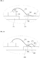
FIGS. 3A and3B are views showing wire bonding structures of a light emitting device package according to other embodiments; -
FIG. 4A is a perspective view showing a lighting apparatus including a light emitting device package according to an embodiment; -
FIG. 4B is a sectional view taken along line D-D' ofFIG. 4A ; -
FIG. 5 is an exploded perspective view showing a backlight unit including a light emitting device package according to an embodiment; and -
FIG. 6 is an exploded perspective view showing a backlight unit including a light emitting device package according to another embodiment. - Reference will now be made in detail to embodiments, examples of which are illustrated in the accompanying drawings. However, the present disclosure may be embodied in many different forms and should not be construed as limited to the embodiments set forth herein. Rather, these embodiments are provided so that this disclosure will be thorough and complete, and will fully convey the scope of the disclosure to those skilled in the art. The present disclosure is defined only by the categories of the claims. In certain embodiments, detailed descriptions of device constructions or processes well known in the art may be omitted to avoid obscuring appreciation of the disclosure by a person of ordinary skill in the art. Wherever possible, the same reference numbers will be used throughout the drawings to refer to the same or like parts.
- Spatially-relative terms such as "below", "beneath", "lower", "above", or "upper" may be used herein to describe one element's relationship to another element as illustrated in the figures. It will be understood that spatially-relative terms are intended to encompass different orientations of the device in addition to the orientation depicted in the figures. For example, if the device in one of the figures is turned over, elements described as "below" or "beneath" other elements would then be oriented "above" the other elements. The exemplary terms "below" or "beneath" can, therefore, encompass both an orientation of above and below. Since the device may be oriented in another direction, the spatially-relative terms may be interpreted in accordance with the orientation of the device.
- The terminology used in the present disclosure is for the purpose of describing particular embodiments only and is not intended to limit the disclosure. As used in the disclosure and the appended claims, the singular forms "a", "an" and "the" are intended to include the plural forms as well, unless context clearly indicate s otherwise. It will be further understood that the terms "comprises" and/or "comprising," when used in this specification, specify the presence of stated features, integers, steps, operations, elements, and/or components, but do not preclude the presence or addition of one or more other features, integers, steps, operations, elements, components, and/or groups thereof.
- Unless otherwise defined, all terms (including technical and scientific terms) used herein have the same meaning as commonly understood by one of ordinary skill in the art. It will be further understood that terms, such as those defined in commonly used dictionaries, should be interpreted as having a meaning that is consistent with their meaning in the context of the relevant art and the present disclosure, and will not be interpreted in an idealized or overly formal sense unless expressly so defined herein.
- In the drawings, the thickness or size of each layer is exaggerated, omitted, or schematically illustrated for convenience of description and clarity. Also, the size or area of each constituent element does not entirely reflect the actual size thereof.
- Angles or directions used to describe the structures of light emitting devices according to embodiments are based on those shown in the drawings. Unless there is, in the specification, no definition of a reference point to describe angular positional relations in the structures of the light emitting devices, the associated drawings may be referred to.
-
FIG. 1 is a sectional view showing a light emitting device package according to an embodiment. - Referring to
FIG. 1 , a lightemitting device package 100 may include apackage body 110 having a cavity, alight emitting device 130 mounted in the cavity, alead frame 120, and aresin 140 filled in the cavity. - The
package body 110 may function as a housing. The cavity may be formed in the center of thepackage body 110 so that thelight emitting device 130 is mounted in the cavity. - Also, the
package body 110 may wrap thelead frame 120 to support thelead frame 120. Thepackage body 110 may be formed of at least one selected from among a resin material such as polyphthalamide (PPA), silicon (Si), aluminum (Al), aluminum nitride (AlN), liquid crystal polymer, photo sensitive glass (PSG), polyamide 9T (PA9T), syndiotactic polystyrene (SPS), a metallic material, a sapphire (Al203), beryllium oxide (BeO), and a printed circuit board (PCB). Thepackage body 110 may be formed by injection molding or etching. However, the disclosure is not limited thereto. - The cavity may be formed in the
package body 110 in a state in which the upper side of the cavity is open so that thelight emitting device 130 is exposed outward through the cavity. The cavity may be tilted in thepackage body 110. A reflection angle of light emitted from thelight emitting device 130 may vary based on a tilt angle, thereby adjusting a view angle of light emitted outward. - If a view angle of light decreases, concentration of light emitted from the
light emitting device 130 increases. On the other hand, if a view angle of light increases, concentration of light emitted from thelight emitting device 130 decreases. - Meanwhile, the cavity formed in the
package body 110 may be formed in a circular shape, a quadrangular shape, a polygonal shape or an oval shape when viewed from above. In particular, the edge of the cavity may be curved. However, the disclosure is not limited thereto. - A reflective coating layer (not shown) may be formed at an inner side surface, constituting an inner wall of the cavity, and bottom surface of the cavity. The surface of the
package 110, at which the reflective coating layer (not shown) is formed, may have predetermined roughness. The surface of thepackage 110 may be formed of silver (Ag) or aluminum (Al). - The
lead frame 120 may be formed of at least one selected from among titanium (Ti), copper (Cu), nickel (Ni), gold (Au), chrome (Cr), tantalum (Ta), platinum (Pt), tin (Sn), silver (Ag), phosphorus (P), aluminum (Al), indium (In), palladium (Pd), cobalt (Co), silicon (Si), germanium (Ge), hafnium (Hf), ruthenium (Ru), and iron (Fe) or an alloy thereof. Also, thelead frame 120 may have a single layer structure or a multi layer structure. However, the disclosure is not limited thereto. - The
lead frame 120 may include afirst lead frame 121 and asecond lead frame 122, via which different powers may be applied. Thefirst lead frame 121 and thesecond lead frame 122 may be spaced from each other by a predetermined distance. Thefirst lead frame 121 and thesecond lead frame 122 may be partially wrapped by thepackage body 110. - The
light emitting device 130 is mounted at the upper surface of thefirst lead frame 121 or thesecond lead frame 122. Thelight emitting device 130 may be a kind of semiconductor device emitting light having a predetermined wavelength when external power is applied to thelight emitting device 130. Thelight emitting device 130 may be formed of a III or V group compound, such as gallium nitride (GaN), aluminum nitride (AlN), indium nitride (InN), or gallium arsenic (GaAs). For example, thelight emitting device 130 may be a light emitting diode. - The light emitting diode may be a colored light emitting diode to emit red, green, blue or white light or an ultraviolet (UV) light emitting diode to emit UV light. However, the disclosure is not limited thereto. In this embodiment, a single light emitting diode is provided at the center of the light emitting device package. However, the disclosure is not limited thereto. The light emitting device package may include a plurality of light emitting diodes.
- Also, the light emitting device may be a horizontal type light emitting device in which electrical terminals are formed at the upper surface of the light emitting device or a vertical type light emitting device in which electrical terminals are formed at the upper and lower surfaces of the light emitting device.
- The horizontal type light emitting device is electrically connected to the
first lead frame 121 and thesecond lead frame 122 by wire bonding using two wires so that external power is applied to the light emitting device. On the other hand, the vertical type light emitting device is electrically connected to thefirst lead frame 121 and thesecond lead frame 122 by wire bonding using one wire so that external power is applied to the light emitting device. - The
resin 140 may be filled in the cavity so as to seal thelight emitting device 130 and the wire. Theresin 140 may be formed of a light transmitting resin material, such as silicone or epoxy. The light transmitting resin material may be filled in the cavity and may be UV or thermally cured to form theresin 140. - The surface of the
resin 140 may be formed in a concave lens shape, a convex lens shape or a flat shape. A view angle of light emitted from thelight emitting device 130 may vary based on the shape of theresin 140. - Also, another resin formed in another lens shape may be formed on or fixed to the top of the
resin 140. However, the disclosure is not limited thereto. - The
resin 140 may contain a fluorescent substance. The kind of the fluorescent substance may be selected based on the wavelength of light emitted from thelight emitting device 130 so that the light emittingdevice package 100 emits white light. - That is, the fluorescent substance may be excited by first light emitted from the
light emitting device 130 to generate second light. For example, if thelight emitting device 130 is a blue light emitting diode and the fluorescent substance is a yellow fluorescent substance, the yellow fluorescent substance may be excited by the blue light to emit yellow light, and the blue light generated from the blue light emitting diode and the yellow light excited by the blue light may be mixed. As a result, the light emittingdevice package 100 emits white light. - In a similar manner, if the
light emitting device 130 is a green light emitting diode, a magenta fluorescent substance or blue and red fluorescent substances may be mixed. Also, if thelight emitting device 130 is a red light emitting diode, a cyan fluorescent substance or blue and green fluorescent substances may be mixed. - The fluorescent substances may be well-known fluorescent substances, such as a YAG fluorescent substance, a TAG fluorescent substance, a sulfide fluorescent substance, a silicate fluorescent substance, an aluminate fluorescent substance, a nitride fluorescent substance, a carbide fluorescent substance, a nitridosilicate fluorescent substance, a borate fluorescent substance, a fluoride fluorescent substance, and a phosphate fluorescent substance.
- Hereinafter, a wire bonding structure encircled by a portion A of
FIG. 1 will be described in detail. -
FIG. 2 is a view showing a wire bonding structure of the light emitting device package according to the embodiment. - Referring to
FIG. 2 , primary bonding to bond a wire to thelight emitting device 130 and secondary bonding to bond the wire connected as the result of the primary bonding to thesecond lead frame 122 are needed so as to electrically connect thelight emitting device 130 positioned on thefirst frame 121 to thesecond lead frame 122. The wire bonding structure may include thelight emitting device 130, anelectrode pad 150, apad ball 160, afirst wire 170, afirst bonding ball 190, asecond bonding ball 195, thefirst lead frame 121, and thesecond lead frame 122. - The
light emitting device 130 may be positioned on thefirst lead frame 121. Thefirst lead frame 121 and thelight emitting device 130 were described previously with reference toFIG. 1 , and therefore, a further description thereof will not be given. - The
electrode pad 150 may be formed at the upper surface of thelight emitting device 130. - The
electrode pad 150 may be formed of a conductive material. For example, theelectrode pad 150 may be formed of any one selected from among indium (In), cobalt (Co), silicon (Si), germanium (Ge), gold (Au), palladium (Pd), platinum (Pt), ruthenium (Ru), rhenium (Re), magnesium (Mg), zinc (Zn), hafnium (Hf), tantalum (Ta), rhodium (Rh), iridium (Ir), tungsten (W), titanium (Ti), silver (Ag), chrome (Cr), molybdenum (Mo), niobium (Nb), aluminum (Al), nickel (Ni), and copper (Cu) or an alloy of two or more thereof. Two or more different materials may be stacked to form theelectrode pad 150. - The
pad ball 160 may be formed on theelectrode pad 150. The wire is electrically discharged using a capillary with the result that thepad ball 160 is formed at one end of the wire. Ultrasonic waves and pressure are applied to thepad ball 160 and theelectrode pad 150 in a state in which thepad ball 160 is in contact with the surface of theelectrode pad 150. As a result, metal bonding between theelectrode pad 150 and thepad ball 160 is achieved. Bonding intensity may vary depending upon intensity of ultrasonic waves, load applied to the pad ball, application time of ultrasonic waves, etc. - For example, if the intensity of ultrasonic waves or load applied to the
pad ball 160 is high, bonding intensity increases. In this case, however, theelectrode pad 150 may be damaged with the result that reliability may be deteriorated. - After the
pad ball 160 is formed, the capillary may move to above thesecond lead frame 122 so as to form a loop using thefirst wire 170. - The
first wire 170 may be a gold wire, a silver wire, an aluminum wire, or a copper wire. The loop formed using the wire may be classified as a high loop, a middle loop, or a low loop based on height of the loop. The high loop wire may be used to perform bonding so that the edge of the light emitting device or the light emitting device package does not contact the wire since the height of the loop is high but the length of the loop is short. On the other hand, the low loop wire may be used in a thin light emitting device package since a crystalline region is shorted so that the height of the loop is low. - The diameter of the
first wire 170 decides the magnitude of current that can flow along thefirst wire 170. Consequently, required current and voltage may be calculated to decide the size of thefirst wire 170. - In this embodiment, the
first wire 170 may have a diameter of 0.7 mil to 2 mil. - After the
first wire 170 is stitch bonded to thesecond lead frame 122, thefirst wire 170 may be pressed by the capillary so that thefirst wire 170 is cut and fixed to the top of thesecond lead frame 122. - An adhesive (not shown) may be applied to a
first contact point 180 between thefirst wire 170 and thesecond lead frame 122. - The adhesive (not shown) may be a conductive adhesive. The adhesive may be formed of a thermally curable epoxy resin and metal powder such as silver (Ag) or copper (Cu). The adhesive may be adhered in the form of a ball. Upon application of the adhesive, the adhesion force at the
first contact point 180 increases. Although thefirst wire 170 and thesecond lead frame 122 are separated from each other at thefirst contact point 180, current continues to flow betweenfirst wire 170 and thesecond lead frame 122 since the adhesive exhibits conductivity. - The
first bonding ball 190 may be positioned on thesecond lead frame 122 in a state in which thefirst bonding ball 190 is spaced apart from thefirst contact point 180. - If the
first bonding ball 190 is formed of a conductive material and is spaced apart from thefirst contact point 180, thefirst wire 170 is electrically connected to thesecond lead frame 122 at a contact point between thefirst bonding ball 190 and thesecond lead frame 122 as well as at thefirst contact point 180. - Even when the
first wire 170 and thesecond lead frame 122 are separated from each other at thefirst contact point 180, therefore, electrical connection between thefirst wire 170 and thesecond lead frame 122 is maintained by thefirst bonding ball 190, thereby improving reliability of wire bonding. - The distance between the center of the
first bonding ball 190 and thefirst contact point 180 may be 20 um to 50 um. If the distance between the center of thefirst bonding ball 190 and thefirst contact point 180 is less than 20 um, thefirst wire 170 may be separated from thefirst contact point 180 due to the height of thefirst bonding ball 190. On the other hand, if the distance between the center of thefirst bonding ball 190 and thefirst contact point 180 is greater than 50 um, thefirst wire 170 is bent at thefirst bonding ball 190 with the result that adhesion force between thefirst wire 170 and thefirst bonding ball 190 is lowered. - The
second bonding ball 195 may be positioned above thefirst bonding ball 190 so that thefirst wire 170 is disposed between thesecond bonding ball 195 and thefirst bonding ball 190 to fix thefirst wire 170. - When the
first wire 170 is fixed using thefirst bonding ball 190 and thesecond bonding ball 195 as described above, separation of thefirst wire 170 from thefirst bonding ball 190 is prevented, and external impact applied to the wire bonded portion at thefirst contact point 180 is relieved, thereby improving reliability of wire bonding. - Also, the
first wire 170 is pushed by thesecond bonding ball 195 with the result that thefirst wire 170 is softly connected to thefirst contact point 180, thereby preventing separation of thefirst wire 170 from thesecond lead frame 122 at thefirst contact point 180. - The
first bonding ball 190 and thesecond bonding ball 195 may be formed of a conductive material, such as Ag, Cu, Al or Au. - The size of the
second bonding ball 195 may be greater than that of thefirst bonding ball 190. - The
first bonding ball 190 may have a width of 95 um to 105 um, and thesecond bonding ball 195 may have a width of 76 um to 84 um. -
FIGS. 3A and3B are views showing wire bonding structures of a light emitting device package according to other embodiments. - Referring to
FIGS. 3A and3B , asecond wire 275 may be provided at afirst bonding ball 290 or asecond bonding ball 295 so that thefirst bonding ball 290 or thesecond bonding ball 295 is electrically connected to asecond lead frame 222 via thesecond wire 275. - The
second wire 275 may be electrically connected to afirst wire 270 by afirst bonding ball 290 or asecond bonding ball 295. - The
second wire 275 may be formed of the same material for thefirst wire 270 and may be formed using the same method as in thefirst wire 270. Alternatively, thesecond wire 275 may be shorter than thefirst wire 270. If thesecond wire 275 is longer, external impact applied to thesecond wire 275 may become stronger. - A
second contact point 285 between thesecond wire 275 and thesecond lead frame 222 may be spaced apart from afirst contact point 280. - If the
second contact point 285 is spaced apart from thefirst contact point 280, thefirst wire 270 may be electrically connected to thesecond lead frame 222 at thesecond contact point 285 as well as thefirst contact point 280. - Even when the
first wire 270 is separated from thesecond lead frame 222 at thefirst contact point 280, therefore, electrical connection between thefirst wire 270 and thesecond lead frame 222 is maintained by thesecond wire 275 and thefirst bonding ball 290 or by thesecond wire 275 and thesecond bonding ball 295, thereby improving reliability of wire bonding. -
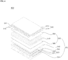
FIG. 4A is a perspective view showing a lighting apparatus including a light emitting device package according to an embodiment, andFIG. 4B is a sectional view taken along line D-D' ofFIG. 4A . - Hereinafter, a
lighting apparatus 200 will be described based on a longitudinal direction Z of thelighting apparatus 200, a horizontal direction Y perpendicular to the longitudinal direction Z, and a height direction X perpendicular to the longitudinal direction Z and the horizontal direction Y so as to describe the shape of thelighting apparatus 200 in more detail. - That is,
FIG. 4B is a sectional view of thelighting apparatus 200 shown inFIG. 4A when thelighting apparatus 200 is cut in the longitudinal direction Z and the height direction X and is viewed in the horizontal direction Y. - Referring to
FIGS. 4A and4B , thelighting apparatus 200 may include anapparatus body 310, acover 330 fastened to theapparatus body 310, and closingcaps 350 provided at opposite ends of theapparatus body 310. - A light emitting
device module 340 is fastened to the lower surface of theapparatus body 310. Theapparatus body 310 may be formed of a metallic material exhibiting high conductivity and heat dissipation to discharge heat generated from light emitting device packages 344 outward through the upper surface of theapparatus body 310. - Several color light emitting device packages 344 may be mounted on a
PCB 342 at several rows to constitute an array. The light emitting device packages 344 may be mounted on thePCB 342 at the same interval or at various intervals as needed so as to adjust brightness of thelighting apparatus 200. A metal core PCB or a PCB formed of an FR4 material may be used as thePCB 342. - Meanwhile, each of the light emitting device packages 344 may include a film, having a plurality of holes, formed of a conductive material.
- The film, formed of the conductive material such as metal, may cause substantial light interference. As a result, intensity of light waves may be increased by interaction of the light waves, and therefore, light is effectively extracted and diffused. Light generated from the light source is interfered and diffracted through the holes formed in the film, and therefore, light is effectively extracted. Consequently, efficiency of the
lighting apparatus 200 is improved. The size of each of the holes formed in the film may be less than the wavelength of light generated from the light source. - The
cover 330 protects the light emittingdevice module 340 from external foreign matter. Also, thecover 330 may contain diffusion particles to prevent glare and to uniformly discharge light outward. In addition, a prism pattern may be formed at the inner surface and/or the outer surface of thecover 330. Also, a florescent substance may be applied to the inner surface and/or the outer surface of thecover 330. - Meanwhile, light generated from the light emitting device packages 344 is discharged outward through the
cover 330. For this reason, it is necessary for thecover 330 to exhibit high light transmissivity and heat resistance sufficient to endure heat generated from the light emitting device packages 344. Thecover 330 may be formed of a material including polyethylene terephthalate (PET), polycarbonate (PC) or polymethyl methacrylate (PMMA). - The closing caps 350 are provided at the opposite ends of the
apparatus body 310 to cover a power supply unit (not shown). Also, power pins 352 are formed at each of the closing caps 350. Consequently, thelighting apparatus 200 according to this embodiment may be directly connected to a terminal, from which the existing fluorescent lamp is removed, without using an additional connection member. -
FIG. 5 is an exploded perspective view showing a backlight unit including a light emitting device package according to an embodiment. - An edge light type backlight unit is shown in
FIG. 5 . A liquidcrystal display apparatus 300 may include a liquidcrystal display panel 410 and abacklight unit 470 to supply light to the liquidcrystal display panel 410. - The liquid
crystal display panel 410 may display an image using light emitted from thebacklight unit 470. The liquidcrystal display panel 410 may include acolor filter substrate 412 and a thinfilm transistor substrate 414 opposite to each other in a state in which a liquid crystal is disposed between thecolor filter substrate 412 and the thinfilm transistor substrate 414. - The
color filter substrate 412 may realize colors of the image displayed through the liquidcrystal display panel 410. - The thin
film transistor substrate 414 is electrically connected to a printedcircuit board 418, on which a plurality of circuit parts is mounted, viadrive films 417. The thinfilm transistor substrate 414 may apply drive voltage supplied from the printedcircuit board 418 to the liquid crystal in response to a drive signal provided by the printedcircuit board 418. - The thin
film transistor substrate 414 may include a thin film transistor and a pixel electrode formed on another transparent substrate, such as glass or plastic. - The
backlight unit 470 includes a light emittingdevice module 420 to emit light, alight guide plate 430 to change the light emitted from the light emittingdevice module 420 into surface emission light and to provide the surface emission light to the liquidcrystal display panel 410, a plurality offilms light guide plate 430, thereby improving vertical incidence of light, and areflective sheet 440 to reflect light emitted to the rear of thelight guide plate 430 to thelight guide plate 430. - The light emitting
device module 420 may include a plurality of light emitting device packages 424 and a PCB 422 on which the light emitting device packages 424 are mounted to constitute an array. - In particular, each of the light emitting device packages 424 includes a film, having a plurality of holes, formed at a light emission surface thereof. As a result, a lens may be omitted, thereby realizing a slim type light emitting device package and, at the same time, improving light extraction efficiency. Consequently, it is possible to realize a very
thin backlight unit 470. - Meanwhile, the
backlight unit 470 may further include adiffusion film 460 to diffuse the light emitted from thelight guide plate 430 toward the liquidcrystal display panel 410 and aprism film 450 to condense the diffused light, thereby improving vertical incidence of light. Also, thebacklight unit 470 may further include aprotection film 464 to protect theprism film 450. -
FIG. 6 is an exploded perspective view showing a backlight unit including a light emitting device package according to another embodiment. - However, parts shown in
FIG. 5 and described with reference toFIG. 5 will not be described in detail. - A direct type backlight unit is shown in
FIG. 6 . A liquidcrystal display apparatus 400 may include a liquidcrystal display panel 510 and a backlight unit 570 to supply light to the liquidcrystal display panel 510. - The liquid
crystal display panel 510 is identical to the liquidcrystal display panel 410 ofFIG. 5 , and therefore, a detailed description thereof will not be given. - The backlight unit 570 may include a plurality of light emitting device modules 523, a
reflective sheet 524, alower chassis 530 in which the light emitting device modules 523 and thereflective sheet 524 are disposed, adiffusion plate 540 disposed above the light emitting device modules 523, and a plurality ofoptical films 560. - Each of the light emitting device modules 523 may include a PCB 531 on which on which a plurality of light emitting device packages 522 is mounted to constitute an array.
- In particular, each of the light emitting device packages 522 includes a conductive film, having a plurality holes, provided at a light emission surface thereof. As a result, a lens may be omitted, thereby realizing a slim type light emitting device package and, at the same time, improving light extraction efficiency. Consequently, it is possible to realize a very thin backlight unit 570.
- The
reflective sheet 524 reflects light emitted from the light emitting device packages 522 toward the liquidcrystal display panel 510, thereby improving luminous efficacy. - Meanwhile, light emitted from the light emitting device modules 523 is incident upon the
diffusion plate 540. Theoptical films 560 are disposed above thediffusion plate 540. Theoptical films 560 include adiffusion film 566, aprism film 550, and aprotection film 564. - As is apparent from the above description, in the light emitting device package and the lighting system including the backlight unit and the lighting apparatus, the wire is fixed using the bonding ball upon wire bonding, thereby preventing the wire from separating from the lead frame at the bonded portion therebetween. Also, the wire is electrically connected to the lead frame via the bonding ball, thereby improving reliability of wire bonding.
- Although embodiments have been described with reference to a number of illustrative embodiments thereof, it should be understood that numerous other modifications and applications may be devised by those skilled in the art that will fall within the intrinsic aspects of the embodiments. More particularly, various variations and modifications are possible in concrete constituent elements of the embodiments. In addition, it is to be understood that differences relevant to the variations and modifications fall within the spirit and scope of the present disclosure defined in the appended claims.
Claims (14)
- A light emitting device package comprising:a light emitting device disposed on a first lead frame, the light emitting device having an electrode pad on an upper surface thereof;a first wire to electrically interconnect a second lead frame spaced apart from the first lead frame and the electrode pad; anda first bonding ball disposed on the second lead frame, the first bonding ball spaced apart from a first contact point, which is in contact with the first wire and the second lead frame, whereinthe first bonding ball is disposed between the first wire and the second lead frame to electrically interconnect the first wire and the second lead frame.
- The light emitting device package according to claim 1, wherein
the light emitting device comprises a pad ball on the electrode pad, and
the first wire electrically interconnects the pad ball and the second lead frame. - The light emitting device package according to claim 1 or 2, further comprising a second bonding ball disposed on the first bonding ball, wherein
the first wire is disposed between the first bonding ball and the second bonding ball so that the first wire is fixed by the first bonding ball and the second bonding ball. - The light emitting device package according to claim 3, wherein the first bonding ball has a width greater than that of the second bonding ball.
- The light emitting device package according to claim 3 or 4, further comprising a second wire to electrically interconnect the first bonding ball or the second bonding ball and the second lead frame.
- The light emitting device package according to claim 5, wherein the first wire or the second wire include at least one selected from among gold, silver, aluminum, and copper.
- The light emitting device package according to claim 5 or 6, wherein a second contact point, which is contact with the second wire and the second lead frame, is spaced apart from the first contact point.
- The light emitting device package according to any one of claims 1 to 7, wherein an adhesive is applied to the first contact point.
- The light emitting device package according to claim 8, wherein the adhesive includes a thermally curable epoxy resin or metal powder.
- The light emitting device package according to any one of claims 3 to 9, wherein the first bonding ball or the second bonding ball include Ag.
- The light emitting device package according to any one of claims 1 to 10, wherein a distance between a center of the first bonding ball and the first contact point is 20 um to 50 um.
- The light emitting device package according to any one of claims 1 to 11, further comprising:a package body having a cavity in which the light emitting device is mounted; anda resin filled in the cavity.
- The light emitting device package according to claim 12, wherein the resin contains a fluorescent substance and/or a light diffuser.
- A lighting system comprising the light emitting device package of any one of claims 1 to 13.
Applications Claiming Priority (1)
| Application Number | Priority Date | Filing Date | Title |
|---|---|---|---|
| KR1020110051340A KR101805118B1 (en) | 2011-05-30 | 2011-05-30 | Light-emitting device |
Publications (3)
| Publication Number | Publication Date |
|---|---|
| EP2530754A2 true EP2530754A2 (en) | 2012-12-05 |
| EP2530754A3 EP2530754A3 (en) | 2015-02-25 |
| EP2530754B1 EP2530754B1 (en) | 2016-12-21 |
Family
ID=45787124
Family Applications (1)
| Application Number | Title | Priority Date | Filing Date |
|---|---|---|---|
| EP12158521.0A Active EP2530754B1 (en) | 2011-05-30 | 2012-03-08 | Light emitting device package and lighting system |
Country Status (4)
| Country | Link |
|---|---|
| US (1) | US8492786B2 (en) |
| EP (1) | EP2530754B1 (en) |
| KR (1) | KR101805118B1 (en) |
| CN (1) | CN102810623B (en) |
Families Citing this family (10)
| Publication number | Priority date | Publication date | Assignee | Title |
|---|---|---|---|---|
| KR102007404B1 (en) * | 2012-12-14 | 2019-08-05 | 엘지이노텍 주식회사 | Light emitting device package |
| US20140209950A1 (en) * | 2013-01-31 | 2014-07-31 | Luxo-Led Co., Limited | Light emitting diode package module |
| JP6136701B2 (en) * | 2013-07-24 | 2017-05-31 | 日亜化学工業株式会社 | Light emitting device |
| KR20150025231A (en) * | 2013-08-28 | 2015-03-10 | 서울반도체 주식회사 | Light source module and manufacturing method thereof, backlight unit |
| CN103972221A (en) * | 2014-06-03 | 2014-08-06 | 宁波升谱光电半导体有限公司 | LED (light-emitting diode) light source packaging structure and method |
| CN107045992A (en) * | 2017-04-19 | 2017-08-15 | 中国科学院上海微系统与信息技术研究所 | Imaging sensor wafer-level encapsulation method and encapsulating structure |
| US10622531B2 (en) | 2017-09-28 | 2020-04-14 | Nichia Corporation | Light-emitting device |
| JP7174218B2 (en) * | 2017-12-27 | 2022-11-17 | 日亜化学工業株式会社 | Light emitting device and manufacturing method thereof |
| CN108506798A (en) * | 2018-03-20 | 2018-09-07 | 京东方科技集团股份有限公司 | Display device and side entering type light source module group |
| CN113035817A (en) * | 2019-12-25 | 2021-06-25 | 上海凯虹科技电子有限公司 | Package body |
Family Cites Families (10)
| Publication number | Priority date | Publication date | Assignee | Title |
|---|---|---|---|---|
| JPS5230231B2 (en) * | 1973-03-26 | 1977-08-06 | ||
| JP3869562B2 (en) | 1998-10-16 | 2007-01-17 | 三洋電機株式会社 | Manufacturing method of semiconductor device |
| JP2001015541A (en) * | 1999-06-28 | 2001-01-19 | Sumitomo Electric Ind Ltd | Semiconductor device and method of manufacturing semiconductor device |
| JP2003197669A (en) * | 2001-12-28 | 2003-07-11 | Seiko Epson Corp | Bonding method and bonding apparatus |
| JP3888438B2 (en) * | 2002-02-25 | 2007-03-07 | セイコーエプソン株式会社 | Semiconductor device and manufacturing method thereof, circuit board, and electronic apparatus |
| US20030230796A1 (en) | 2002-06-12 | 2003-12-18 | Aminuddin Ismail | Stacked die semiconductor device |
| CN100347867C (en) * | 2004-02-26 | 2007-11-07 | 元砷光电科技股份有限公司 | Technique of solder ball for manufacutirng LED |
| JP5008832B2 (en) * | 2005-04-15 | 2012-08-22 | ローム株式会社 | Semiconductor device and manufacturing method of semiconductor device |
| US7476608B2 (en) * | 2005-07-14 | 2009-01-13 | Hewlett-Packard Development Company, L.P. | Electrically connecting substrate with electrical device |
| KR101488448B1 (en) * | 2007-12-06 | 2015-02-02 | 서울반도체 주식회사 | Led package and method for fabricating the same |
-
2011
- 2011-05-30 KR KR1020110051340A patent/KR101805118B1/en not_active Expired - Fee Related
-
2012
- 2012-03-05 US US13/412,024 patent/US8492786B2/en active Active
- 2012-03-08 EP EP12158521.0A patent/EP2530754B1/en active Active
- 2012-03-27 CN CN201210083699.3A patent/CN102810623B/en active Active
Non-Patent Citations (1)
| Title |
|---|
| None |
Also Published As
| Publication number | Publication date |
|---|---|
| CN102810623A (en) | 2012-12-05 |
| US20120305962A1 (en) | 2012-12-06 |
| CN102810623B (en) | 2017-03-01 |
| KR101805118B1 (en) | 2017-12-05 |
| EP2530754B1 (en) | 2016-12-21 |
| EP2530754A3 (en) | 2015-02-25 |
| KR20120132931A (en) | 2012-12-10 |
| US8492786B2 (en) | 2013-07-23 |
Similar Documents
| Publication | Publication Date | Title |
|---|---|---|
| US8492786B2 (en) | Light emitting device package and lighting system | |
| EP2587561A2 (en) | Light source module | |
| US9491856B2 (en) | Light emitting device array and light system | |
| US9202806B2 (en) | Light emitting device package | |
| EP2458655A2 (en) | Light emitting device package | |
| KR101941512B1 (en) | Light emitting device | |
| KR20130079921A (en) | Printed circuit board | |
| KR101920211B1 (en) | Light emitting device array | |
| KR101849126B1 (en) | Light Emitting Device Package | |
| KR20120071150A (en) | Light emitting device package | |
| KR102042208B1 (en) | Printed Circuit Board | |
| KR101781047B1 (en) | Light emitting device package | |
| KR102075522B1 (en) | Light-emitting device | |
| KR101818752B1 (en) | Light emitting device array | |
| KR20120071151A (en) | Light emitting package | |
| KR101831278B1 (en) | Light-emitting device | |
| KR101894933B1 (en) | Light Emitting Device Package | |
| KR20130061421A (en) | Light emitting package | |
| KR20120073932A (en) | Light emitting element array | |
| KR20120034484A (en) | Light emitting device package | |
| KR20120014490A (en) | Light emitting device package including a lead frame | |
| KR20120037264A (en) | Light emitting device package | |
| KR20120087581A (en) | Light emitting device package | |
| KR20120035464A (en) | Light emitting device package | |
| KR20150054266A (en) | Light emitting device package |
Legal Events
| Date | Code | Title | Description |
|---|---|---|---|
| PUAI | Public reference made under article 153(3) epc to a published international application that has entered the european phase |
Free format text: ORIGINAL CODE: 0009012 |
|
| AK | Designated contracting states |
Kind code of ref document: A2 Designated state(s): AL AT BE BG CH CY CZ DE DK EE ES FI FR GB GR HR HU IE IS IT LI LT LU LV MC MK MT NL NO PL PT RO RS SE SI SK SM TR |
|
| AX | Request for extension of the european patent |
Extension state: BA ME |
|
| PUAL | Search report despatched |
Free format text: ORIGINAL CODE: 0009013 |
|
| AK | Designated contracting states |
Kind code of ref document: A3 Designated state(s): AL AT BE BG CH CY CZ DE DK EE ES FI FR GB GR HR HU IE IS IT LI LT LU LV MC MK MT NL NO PL PT RO RS SE SI SK SM TR |
|
| AX | Request for extension of the european patent |
Extension state: BA ME |
|
| RIC1 | Information provided on ipc code assigned before grant |
Ipc: H01L 33/60 20100101ALN20150120BHEP Ipc: H01L 33/48 20100101ALN20150120BHEP Ipc: H01L 33/62 20100101AFI20150120BHEP |
|
| 17P | Request for examination filed |
Effective date: 20150821 |
|
| RBV | Designated contracting states (corrected) |
Designated state(s): AL AT BE BG CH CY CZ DE DK EE ES FI FR GB GR HR HU IE IS IT LI LT LU LV MC MK MT NL NO PL PT RO RS SE SI SK SM TR |
|
| 17Q | First examination report despatched |
Effective date: 20160128 |
|
| GRAP | Despatch of communication of intention to grant a patent |
Free format text: ORIGINAL CODE: EPIDOSNIGR1 |
|
| RIC1 | Information provided on ipc code assigned before grant |
Ipc: H01L 23/00 20060101ALI20160621BHEP Ipc: F21K 99/00 20160101ALN20160621BHEP Ipc: H01L 25/075 20060101ALN20160621BHEP Ipc: F21Y 113/00 20160101ALN20160621BHEP Ipc: H01L 33/62 20100101AFI20160621BHEP Ipc: H01L 33/60 20100101ALN20160621BHEP Ipc: H01L 33/48 20100101ALN20160621BHEP |
|
| INTG | Intention to grant announced |
Effective date: 20160718 |
|
| GRAS | Grant fee paid |
Free format text: ORIGINAL CODE: EPIDOSNIGR3 |
|
| GRAA | (expected) grant |
Free format text: ORIGINAL CODE: 0009210 |
|
| AK | Designated contracting states |
Kind code of ref document: B1 Designated state(s): AL AT BE BG CH CY CZ DE DK EE ES FI FR GB GR HR HU IE IS IT LI LT LU LV MC MK MT NL NO PL PT RO RS SE SI SK SM TR |
|
| REG | Reference to a national code |
Ref country code: GB Ref legal event code: FG4D |
|
| REG | Reference to a national code |
Ref country code: CH Ref legal event code: EP |
|
| REG | Reference to a national code |
Ref country code: IE Ref legal event code: FG4D |
|
| REG | Reference to a national code |
Ref country code: AT Ref legal event code: REF Ref document number: 856173 Country of ref document: AT Kind code of ref document: T Effective date: 20170115 |
|
| REG | Reference to a national code |
Ref country code: DE Ref legal event code: R096 Ref document number: 602012026767 Country of ref document: DE |
|
| PG25 | Lapsed in a contracting state [announced via postgrant information from national office to epo] |
Ref country code: LV Free format text: LAPSE BECAUSE OF FAILURE TO SUBMIT A TRANSLATION OF THE DESCRIPTION OR TO PAY THE FEE WITHIN THE PRESCRIBED TIME-LIMIT Effective date: 20161221 |
|
| REG | Reference to a national code |
Ref country code: NL Ref legal event code: FP |
|
| REG | Reference to a national code |
Ref country code: LT Ref legal event code: MG4D |
|
| PG25 | Lapsed in a contracting state [announced via postgrant information from national office to epo] |
Ref country code: GR Free format text: LAPSE BECAUSE OF FAILURE TO SUBMIT A TRANSLATION OF THE DESCRIPTION OR TO PAY THE FEE WITHIN THE PRESCRIBED TIME-LIMIT Effective date: 20170322 Ref country code: SE Free format text: LAPSE BECAUSE OF FAILURE TO SUBMIT A TRANSLATION OF THE DESCRIPTION OR TO PAY THE FEE WITHIN THE PRESCRIBED TIME-LIMIT Effective date: 20161221 Ref country code: LT Free format text: LAPSE BECAUSE OF FAILURE TO SUBMIT A TRANSLATION OF THE DESCRIPTION OR TO PAY THE FEE WITHIN THE PRESCRIBED TIME-LIMIT Effective date: 20161221 Ref country code: NO Free format text: LAPSE BECAUSE OF FAILURE TO SUBMIT A TRANSLATION OF THE DESCRIPTION OR TO PAY THE FEE WITHIN THE PRESCRIBED TIME-LIMIT Effective date: 20170321 |
|
| REG | Reference to a national code |
Ref country code: AT Ref legal event code: MK05 Ref document number: 856173 Country of ref document: AT Kind code of ref document: T Effective date: 20161221 |
|
| RAP2 | Party data changed (patent owner data changed or rights of a patent transferred) |
Owner name: LG INNOTEK CO., LTD. |
|
| PG25 | Lapsed in a contracting state [announced via postgrant information from national office to epo] |
Ref country code: HR Free format text: LAPSE BECAUSE OF FAILURE TO SUBMIT A TRANSLATION OF THE DESCRIPTION OR TO PAY THE FEE WITHIN THE PRESCRIBED TIME-LIMIT Effective date: 20161221 Ref country code: RS Free format text: LAPSE BECAUSE OF FAILURE TO SUBMIT A TRANSLATION OF THE DESCRIPTION OR TO PAY THE FEE WITHIN THE PRESCRIBED TIME-LIMIT Effective date: 20161221 Ref country code: FI Free format text: LAPSE BECAUSE OF FAILURE TO SUBMIT A TRANSLATION OF THE DESCRIPTION OR TO PAY THE FEE WITHIN THE PRESCRIBED TIME-LIMIT Effective date: 20161221 |
|
| PG25 | Lapsed in a contracting state [announced via postgrant information from national office to epo] |
Ref country code: CZ Free format text: LAPSE BECAUSE OF FAILURE TO SUBMIT A TRANSLATION OF THE DESCRIPTION OR TO PAY THE FEE WITHIN THE PRESCRIBED TIME-LIMIT Effective date: 20161221 Ref country code: SK Free format text: LAPSE BECAUSE OF FAILURE TO SUBMIT A TRANSLATION OF THE DESCRIPTION OR TO PAY THE FEE WITHIN THE PRESCRIBED TIME-LIMIT Effective date: 20161221 Ref country code: EE Free format text: LAPSE BECAUSE OF FAILURE TO SUBMIT A TRANSLATION OF THE DESCRIPTION OR TO PAY THE FEE WITHIN THE PRESCRIBED TIME-LIMIT Effective date: 20161221 Ref country code: IS Free format text: LAPSE BECAUSE OF FAILURE TO SUBMIT A TRANSLATION OF THE DESCRIPTION OR TO PAY THE FEE WITHIN THE PRESCRIBED TIME-LIMIT Effective date: 20170421 Ref country code: RO Free format text: LAPSE BECAUSE OF FAILURE TO SUBMIT A TRANSLATION OF THE DESCRIPTION OR TO PAY THE FEE WITHIN THE PRESCRIBED TIME-LIMIT Effective date: 20161221 |
|
| PG25 | Lapsed in a contracting state [announced via postgrant information from national office to epo] |
Ref country code: SM Free format text: LAPSE BECAUSE OF FAILURE TO SUBMIT A TRANSLATION OF THE DESCRIPTION OR TO PAY THE FEE WITHIN THE PRESCRIBED TIME-LIMIT Effective date: 20161221 Ref country code: PT Free format text: LAPSE BECAUSE OF FAILURE TO SUBMIT A TRANSLATION OF THE DESCRIPTION OR TO PAY THE FEE WITHIN THE PRESCRIBED TIME-LIMIT Effective date: 20170421 Ref country code: IT Free format text: LAPSE BECAUSE OF FAILURE TO SUBMIT A TRANSLATION OF THE DESCRIPTION OR TO PAY THE FEE WITHIN THE PRESCRIBED TIME-LIMIT Effective date: 20161221 Ref country code: BE Free format text: LAPSE BECAUSE OF FAILURE TO SUBMIT A TRANSLATION OF THE DESCRIPTION OR TO PAY THE FEE WITHIN THE PRESCRIBED TIME-LIMIT Effective date: 20161221 Ref country code: BG Free format text: LAPSE BECAUSE OF FAILURE TO SUBMIT A TRANSLATION OF THE DESCRIPTION OR TO PAY THE FEE WITHIN THE PRESCRIBED TIME-LIMIT Effective date: 20170321 Ref country code: AT Free format text: LAPSE BECAUSE OF FAILURE TO SUBMIT A TRANSLATION OF THE DESCRIPTION OR TO PAY THE FEE WITHIN THE PRESCRIBED TIME-LIMIT Effective date: 20161221 Ref country code: ES Free format text: LAPSE BECAUSE OF FAILURE TO SUBMIT A TRANSLATION OF THE DESCRIPTION OR TO PAY THE FEE WITHIN THE PRESCRIBED TIME-LIMIT Effective date: 20161221 Ref country code: PL Free format text: LAPSE BECAUSE OF FAILURE TO SUBMIT A TRANSLATION OF THE DESCRIPTION OR TO PAY THE FEE WITHIN THE PRESCRIBED TIME-LIMIT Effective date: 20161221 |
|
| REG | Reference to a national code |
Ref country code: DE Ref legal event code: R097 Ref document number: 602012026767 Country of ref document: DE |
|
| PLBE | No opposition filed within time limit |
Free format text: ORIGINAL CODE: 0009261 |
|
| STAA | Information on the status of an ep patent application or granted ep patent |
Free format text: STATUS: NO OPPOSITION FILED WITHIN TIME LIMIT |
|
| REG | Reference to a national code |
Ref country code: CH Ref legal event code: PL |
|
| 26N | No opposition filed |
Effective date: 20170922 |
|
| GBPC | Gb: european patent ceased through non-payment of renewal fee |
Effective date: 20170321 |
|
| PG25 | Lapsed in a contracting state [announced via postgrant information from national office to epo] |
Ref country code: MC Free format text: LAPSE BECAUSE OF FAILURE TO SUBMIT A TRANSLATION OF THE DESCRIPTION OR TO PAY THE FEE WITHIN THE PRESCRIBED TIME-LIMIT Effective date: 20161221 Ref country code: DK Free format text: LAPSE BECAUSE OF FAILURE TO SUBMIT A TRANSLATION OF THE DESCRIPTION OR TO PAY THE FEE WITHIN THE PRESCRIBED TIME-LIMIT Effective date: 20161221 |
|
| REG | Reference to a national code |
Ref country code: IE Ref legal event code: MM4A |
|
| REG | Reference to a national code |
Ref country code: FR Ref legal event code: ST Effective date: 20171130 |
|
| PG25 | Lapsed in a contracting state [announced via postgrant information from national office to epo] |
Ref country code: FR Free format text: LAPSE BECAUSE OF NON-PAYMENT OF DUE FEES Effective date: 20170331 Ref country code: LU Free format text: LAPSE BECAUSE OF NON-PAYMENT OF DUE FEES Effective date: 20170308 |
|
| PG25 | Lapsed in a contracting state [announced via postgrant information from national office to epo] |
Ref country code: GB Free format text: LAPSE BECAUSE OF NON-PAYMENT OF DUE FEES Effective date: 20170321 Ref country code: SI Free format text: LAPSE BECAUSE OF FAILURE TO SUBMIT A TRANSLATION OF THE DESCRIPTION OR TO PAY THE FEE WITHIN THE PRESCRIBED TIME-LIMIT Effective date: 20161221 Ref country code: LI Free format text: LAPSE BECAUSE OF NON-PAYMENT OF DUE FEES Effective date: 20170331 Ref country code: CH Free format text: LAPSE BECAUSE OF NON-PAYMENT OF DUE FEES Effective date: 20170331 Ref country code: IE Free format text: LAPSE BECAUSE OF NON-PAYMENT OF DUE FEES Effective date: 20170308 |
|
| PG25 | Lapsed in a contracting state [announced via postgrant information from national office to epo] |
Ref country code: MT Free format text: LAPSE BECAUSE OF NON-PAYMENT OF DUE FEES Effective date: 20170308 |
|
| PG25 | Lapsed in a contracting state [announced via postgrant information from national office to epo] |
Ref country code: HU Free format text: LAPSE BECAUSE OF FAILURE TO SUBMIT A TRANSLATION OF THE DESCRIPTION OR TO PAY THE FEE WITHIN THE PRESCRIBED TIME-LIMIT; INVALID AB INITIO Effective date: 20120308 |
|
| PG25 | Lapsed in a contracting state [announced via postgrant information from national office to epo] |
Ref country code: CY Free format text: LAPSE BECAUSE OF NON-PAYMENT OF DUE FEES Effective date: 20161221 |
|
| PG25 | Lapsed in a contracting state [announced via postgrant information from national office to epo] |
Ref country code: MK Free format text: LAPSE BECAUSE OF FAILURE TO SUBMIT A TRANSLATION OF THE DESCRIPTION OR TO PAY THE FEE WITHIN THE PRESCRIBED TIME-LIMIT Effective date: 20161221 |
|
| PG25 | Lapsed in a contracting state [announced via postgrant information from national office to epo] |
Ref country code: TR Free format text: LAPSE BECAUSE OF FAILURE TO SUBMIT A TRANSLATION OF THE DESCRIPTION OR TO PAY THE FEE WITHIN THE PRESCRIBED TIME-LIMIT Effective date: 20161221 |
|
| PG25 | Lapsed in a contracting state [announced via postgrant information from national office to epo] |
Ref country code: AL Free format text: LAPSE BECAUSE OF FAILURE TO SUBMIT A TRANSLATION OF THE DESCRIPTION OR TO PAY THE FEE WITHIN THE PRESCRIBED TIME-LIMIT Effective date: 20161221 |
|
| REG | Reference to a national code |
Ref country code: NL Ref legal event code: PD Owner name: SUZHOU LEKIN SEMICONDUCTOR CO., LTD.; CN Free format text: DETAILS ASSIGNMENT: CHANGE OF OWNER(S), ASSIGNMENT; FORMER OWNER NAME: LG INNOTEK CO., LTD. Effective date: 20210719 |
|
| REG | Reference to a national code |
Ref country code: DE Ref legal event code: R081 Ref document number: 602012026767 Country of ref document: DE Owner name: SUZHOU LEKIN SEMICONDUCTOR CO. LTD., TAICANG, CN Free format text: FORMER OWNER: LG INNOTEK CO., LTD., SEOUL/SOUL, KR |
|
| PGFP | Annual fee paid to national office [announced via postgrant information from national office to epo] |
Ref country code: NL Payment date: 20230215 Year of fee payment: 12 |
|
| REG | Reference to a national code |
Ref country code: NL Ref legal event code: MM Effective date: 20240401 |
|
| REG | Reference to a national code |
Ref country code: DE Ref legal event code: R079 Ref document number: 602012026767 Country of ref document: DE Free format text: PREVIOUS MAIN CLASS: H01L0033620000 Ipc: H10H0020857000 |
|
| PG25 | Lapsed in a contracting state [announced via postgrant information from national office to epo] |
Ref country code: NL Free format text: LAPSE BECAUSE OF NON-PAYMENT OF DUE FEES Effective date: 20240401 |
|
| PG25 | Lapsed in a contracting state [announced via postgrant information from national office to epo] |
Ref country code: NL Free format text: LAPSE BECAUSE OF NON-PAYMENT OF DUE FEES Effective date: 20240401 |
|
| PGFP | Annual fee paid to national office [announced via postgrant information from national office to epo] |
Ref country code: DE Payment date: 20260204 Year of fee payment: 15 |