EP2530554A2 - Tragbare elektronische Vorrichtung - Google Patents
Tragbare elektronische Vorrichtung Download PDFInfo
- Publication number
- EP2530554A2 EP2530554A2 EP12004223A EP12004223A EP2530554A2 EP 2530554 A2 EP2530554 A2 EP 2530554A2 EP 12004223 A EP12004223 A EP 12004223A EP 12004223 A EP12004223 A EP 12004223A EP 2530554 A2 EP2530554 A2 EP 2530554A2
- Authority
- EP
- European Patent Office
- Prior art keywords
- panel
- front panel
- electronic device
- display panel
- adhesive agent
- Prior art date
- Legal status (The legal status is an assumption and is not a legal conclusion. Google has not performed a legal analysis and makes no representation as to the accuracy of the status listed.)
- Granted
Links
Images


Classifications
-
- G—PHYSICS
- G06—COMPUTING OR CALCULATING; COUNTING
- G06F—ELECTRIC DIGITAL DATA PROCESSING
- G06F1/00—Details not covered by groups G06F3/00 - G06F13/00 and G06F21/00
- G06F1/16—Constructional details or arrangements
- G06F1/1613—Constructional details or arrangements for portable computers
- G06F1/1633—Constructional details or arrangements of portable computers not specific to the type of enclosures covered by groups G06F1/1615 - G06F1/1626
- G06F1/1637—Details related to the display arrangement, including those related to the mounting of the display in the housing
-
- G—PHYSICS
- G06—COMPUTING OR CALCULATING; COUNTING
- G06F—ELECTRIC DIGITAL DATA PROCESSING
- G06F1/00—Details not covered by groups G06F3/00 - G06F13/00 and G06F21/00
- G06F1/16—Constructional details or arrangements
- G06F1/1613—Constructional details or arrangements for portable computers
- G06F1/1626—Constructional details or arrangements for portable computers with a single-body enclosure integrating a flat display, e.g. Personal Digital Assistants [PDAs]
Definitions
- the present invention relates to a portable electronic device including an organic electroluminescent display panel.
- OLED panel organic electroluminescent display panel
- a portable electronic device including: an organic electroluminescent display panel; a front panel made of resin, disposed on the front side of the organic electroluminescent display panel, and functioning as the front surface of the electronic device; and an adhesive agent layer formed between the organic electroluminescent display panel and the front panel.
- the organic electroluminescent display panel is fixed to the front panel via the adhesive agent layer.
- the adhesive agent layer 31 can be provided with a sufficient thickness, and thereby the adhesive agent layer can absorb the warp of the front panel. Accordingly, the load applied to the organic electroluminescent display panel can be reduced.
- FIG. 1 is a front view of a portable electronic device 1 according to an embodiment of the present invention.
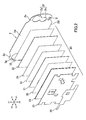
- FIG. 2 is an exploded perspective view of the display panel unit 20 and the front panel 2 of the electronic device 1.
- FIG. 3 is a schematic cross sectional view along the line III-III in FIG. 1 .
- X1-X2 shown in FIG. 1 corresponds to the left-right direction
- Z1-Z2 corresponds to the up-down direction
- Y1-Y2 shown in FIG. 3 corresponds to the front-back direction.
- the electronic device 1 includes a display panel unit 20.
- the electronic device 1 in this example is a portable device that functions as a game device or a motion picture/sound reproduction device.
- the electronic device 1 has, on the front surface thereof, plural operating members to be operated by a user. Specifically, plural (four in this example) operation buttons 5 are disposed to the right of the display panel unit 20. The four buttons 5 are positioned at the respective ends of a cross shape.
- a directional key 6 which has substantially cross shape is disposed to the left of the display panel unit 20.
- Operating sticks 7, 8 are disposed to the right and left, respectively, of the display panel unit 20.
- the operating sticks 7, 8 include stems 7b, 8b that project forward from the electronic device 1, and operated portions 7a, 8a which have disk shape and are attached to the heads of the stems 7b, 8b, respectively.
- the operating sticks 7, 8 can be inclined in radial direction of the stems 7b, 8b, such as in the up-down and left-right direction, and rotated in the circumferential direction of the stems 7b, 8b at a radially inclined posture.
- the operating sticks 7, 8 may be slidable in the radial direction of the stems 7b, 8b.
- the electronic device 1 has upper buttons 14, 15 provided respectively at the rightmost and leftmost positions on the top surface thereof. Still further, the electronic device 1 has buttons 16a, 16b, 16c arranged below the operating sticks 7, 8.
- the display panel unit 20 includes an organic electroluminescent display panel (hereinafter referred as OLED panel) 21.
- the display panel unit 20 in this example further includes a touch panel 22.
- the touch panel 22 is, e.g., a static capacitance type.
- the electronic device 1 further includes a front panel 2.
- the front panel 2 is disposed on the front side of the OLED panel 21, that is, disposed on the front side of the display panel unit 20, and functions as the front surface of the electronic device 1.
- the electronic device 1 has a width in the left-right direction (the left-right width) larger than the width thereof in the up-down direction (the up-down width), as shown in FIG. 1 .
- the front panel 2 as well has a left-right width larger than the up-down width thereof, and has a shape substantially corresponding to the outer shape of the electronic device 1 in the front view of the electronic device 1.
- the front panel 2 is made of light transmissive resin, and has higher shock resistance, compared to glass.
- the front panel 2 in this example includes a first resin layer 2a and a second resin layer 2b formed on the back surface of the first resin layer 2a.
- the second resin layer 2b and the first resin layer 2a are made of different materials.
- the second resin layer 2b is made of material that is less hard than the first resin layer 2a. This can impart increased shock resistance to the front panel 2, while reducing the possibility of damaging the front surface of the front panel 2.
- the first resin layer 2a is made of acryl
- the second resin layer 2b is made of polycarbonate.
- the front panel 2 further includes a third resin layer 2c formed on the back surface of the second resin layer 2b.
- the third resin layer 2c is made of material identical to that of the first resin layer 2a. This can reduce a warp of the front panel 2.
- the first resin layer 2a and the third resin layer 2c are made of acryl. These three resin layers 2a, 2b, 2c are adhered to one another with adhesive agent or the like.
- the display panel unit 20 further includes an adhesive agent layer 31 formed between the OLED panel 21 and the front panel 2.
- the OLED panel 21 is fixed to the front panel 2 via the adhesive agent layer 31. That is, the OLED panel 21 and the front panel 2 are directly or indirectly fixed to each other via the adhesive agent layer 31.
- the adhesive agent layer 31 can be provided with a sufficient thickness, and thereby the warp of the front panel 2 can be absorbed by the adhesive agent layer 31 and a load applied to the OLED panel 21 can be reduced.
- the adhesive agent layer 31 is formed by applied adhesive agent. That is, the adhesive agent layer 31 is formed by applying adhesive agent directly to either one of the OLED panel 21 and a panel facing the OLED panel 21.
- the adhesive agent layer 31 is not an adhesive film including a base film (substrate) and adhesive agent applied on both surfaces of the base film.
- the display panel unit 20 in this example includes, between the OLED panel 21 and the touch panel 22, a wavelength panel 24 for reducing reflection of outside light.
- the adhesive agent layer 31 is formed by applying adhesive agent directly to either one of the front surface of the OLED panel 21 and the back surface of the wavelength panel 24. In this example, the adhesive agent layer 31 is formed by applying adhesive agent to the front surface of the OLED panel 21.
- the adhesive agent layer 31 can be formed using adhesive agent having viscosity lower than that of adhesive agent applied to both surfaces of an adhesive film.
- adhesive agent having viscosity lower than that of adhesive agent applied to both surfaces of an adhesive film.
- gel or liquid adhesive agent can be used as adhesive agent in forming the adhesive agent layer 31.
- the adhesive agent layer 31 is made using gel adhesive agent, such as e. g. , UV curable adhesive agent.
- the adhesive agent layer 31 does not have a substrate (that is base film). This can reduce the thickness of the adhesive agent layer 31, while a sufficient thickness necessary to absorb warp of the front panel 2 being secured in the adhesive agent layer 31.
- the adhesive agent layer 31 in this example is thicker than an adhesive film, to be described later, that is used to adhere the touch panel 22 and the wavelength panel 24 to the front panel 2.
- the adhesive agent layer 31 is formed on the front surface of the OLED panel 21. Therefore, even when a member with a warp is arranged between the OLED panel 21 and the front panel 2, the warp can be absorbed by the adhesive agent layer 31 and thus application of a load to the OLED panel 21 can be reduced.
- the adhesive agent layer 31 is formed on the entire front surface of the OLED panel 21, and no space (an air layer) is left between the OLED panel 21 and the wavelength panel 24. Accordingly, the display panel unit 20 has high transmittance of light from the OLED panel 21.
- the touch panel 22 is adhered to the back surface of the front panel 2 via an adhesive film 32.
- the wavelength panel 24 is adhered to the back surface of the touch panel 22 via an adhesive film (not shown).
- Use of an adhesive film to adhere the touch panel 22 and the wavelength panel 24, as described above, can facilitate the manufacturing process of the display panel unit 20. Since these two adhesive films have a size corresponding to that of the wavelength panel 24 and that of the touch panel 22, no space (an air layer) is left between any members disposed on the front side of the OLED panel 21. With the above, the display panel unit 20 can have high transmittance of light from the OLED panel 21.
- the electronic device 1 members positioned more forward than the OLED panel 21, namely, the base member of the touch panel 22, the wavelength panel 24, and the front panel 2, described above, are all made of resin. Accordingly, the electronic device 1 can have high shock resistance for the OLED panel 21.
- the display panel unit 20 has a frame 23 that is a metal panel provided in order to ensure strength of the display panel unit 20.
- the frame 23 is fixed to the back surface of the OLED panel 21 via an adhesive film 33.
- a sheet like cushion 25 is provided on the back surface of the frame 23.
- the cushion 25 is made of elastic member, such as elastomer, or the like, having elasticity in the thickness direction.
- the cushion 25 as well is adhered to the back surface of the frame 23 via an adhesive film (not shown).
- metal leaf 26 e.g., copper leaf
- the metal leaf 26 shields noise relative to other electronic components (e.g., an antenna) of the electronic device 1.
- the electronic device 1 includes a housing 50 for accommodating various electronic components of the electronic device 1.
- the housing 50 in this example has a back housing 52 for covering the back surface of the circuit board 41 of the electronic device 1 and a front housing 51 to be assembled into the back housing 52 in the front-back direction so as to cover the front surface of the circuit board 41.
- the front panel 2 is disposed on the front side of the front housing 51, and mounted on the front housing 51, as to be described later in detail.
- An accommodating recess 51e having a size corresponding to the thickness of the display panel unit 20 is formed on the front housing 51.
- the display panel unit 20 is accommodated in the accommodating recess 51e.
- the depth of the accommodating recess 51e corresponds to the thickness of the display panel unit 20, and the display panel unit 20 is supported by the base surface of the accommodating recess 51e. That is, the display panel unit 20 is sandwiched by the accommodating recess 51e and the front panel 2. This can improve resistance of the front panel 2 and the display panel unit 20 against an external force applied to the surface of the front panel 2. That is, even when an external force is applied to the surface of the front panel 2, the front panel 2 is less likely dented, and accordingly, the adhesive structure between the members constituting the display panel unit 20 can be prevented from being damaged.
- the front panel 2 is larger than the OLED panel 21 and the touch panel 22, as shown in FIGS. 1 and 2 , and has an outer circumferential portion (indicated by 2d, 2e in FIGS. 1 and 2 ) that is positioned more outward than the outer edge of the panels 21, 22.
- the front panel 2 is disposed on the front side of the front housing 51, and the outer circumferential portion of the front panel 2 is adhered to the front housing 51 via an adhesive film. In this example, the entire outer circumferential portion is adhered to the front housing 51.
- This structure can correct the warp of the front panel 2, and accordingly can reduce a lord applied to the OLED panel 21.
- the OLED panel 21 and the touch panel 22 in this example are rectangular, of which left-right width is larger than the up-down width thereof.
- the front panel 2 as well has a left-right width larger than the up-down width thereof.
- the outer circumferential portion of the front panel 2 includes two first spread portions 2d that spread from the outer edge of the panels 21, 22 upward and downward, respectively, and two second spread portions 2e that spread from the outer edge of the panels 21, 22 leftward and rightward, respectively.
- the second spread portion 2e spreads more largely than the first spread portion 2d does. That is, the width W2 of the second spread portion 2e in the left-right direction is larger than the width W1 of the first spread portion 2d in the up-down direction (see FIG. 1 ).
- the warp of the front panel 2 can be readily corrected, and resistance against an external force applied to the surface of the front panel 2 can be increased.
- the front panel 2 is made of light transmissive resin, as described above. Non-light transmissive coloring agent is applied to the second spread portions 2e and the first spread portions 2d.
- the operating button 5 and the operating stick 7 are disposed to the right of the display panel unit 20.
- the directional key 6 and the operating stick 8 are disposed to the left of the display panel unit 20.
- the second spread portions 2e spread rightward or leftward beyond the positions of the operating members 5, 6, 7, 8.
- the second spread portions 2e have holes 2f formed thereon in which the operating members 5, 6, 7, 8 are arranged. This structure can ensure a sufficient width of the second spread portion 2e. Consequently, the warp of the front panel 2 can be more readily corrected, and the resistance against an external force applied to the surface of the front panel 2 can be further increased.
- the opening 2f has a shape defined by two connected round holes 2g, 2h.
- plural operating buttons 5 and the operating stick 7 are arranged in the two round holes 2g, 2h, respectively.
- the sizes of the two holes 2g, 2h correspond to those of plural buttons 5 and the operating stick 7, respectively. That is, the opening 2h, where the operating stick 7 is disposed, is smaller than the opening 2g. Accordingly, in the second spread portion 2e, a larger area can be ensured for adhering to the front housing 51.
- the directional key 6 and the operating stick 8 are disposed in the two holes 2g, 2h, respectively.
- the sizes of the two holes 2g, 2h correspond to those of the directional key 6 and the operating stick 8, respectively. That is, the opening 2h, where the operating stick 8 is disposed, is smaller than the opening 2g. Further, holes 2i are formed on the second spread portion 2e for the buttons 16a, 16b, 16c to be disposed therein (see FIG. 2 ).
- a projecting portion 51a to be fit inside the opening 2f is formed on the front housing 51.
- An opening 51b is formed on the projecting portion 51a, and the operating members 5, 6, 7, 8 are disposed in the opening 51b.
- the outer shape of the projecting portion 51a corresponds to the inner shape of the opening 2f.
- a flange 51c is formed on the outer circumferential edge of the front housing 51, surrounding the outer circumferential edge of the front panel 2.
- the front panel 2 is fit inside the flange 51c.
- the position of the front panel 2 relative to the front housing 51 is accurately defined by the flange 51c and the projecting portion 51a.
- the relative position between an adhesive film for adhering the front panel 2 to the front housing 51 and the front panel 2 is also accurately defined. With the above, adhesive strength of the front panel 2 relative to the front housing 51 can be ensured.
- the electronic device 1 includes the resin front panel 2 disposed on the front side of the OLED panel 21 and functioning as the front surface of the electronic device 1.
- the display panel unit 20 includes the adhesive agent layer 31 formed between the OLED panel 21 and the front panel 2.
- the OLED panel 21 is fixed to the front panel 2 via the adhesive agent layer 31.
- the adhesive agent layer 31 can absorb a warp of the front panel 2 by providing a sufficient thickness to the adhesive agent layer 31, and accordingly, a load applied to the OLED panel 21 can be reduced.
- a panel member (the wavelength panel 24 in the above description) is provided between the OLED panel 21 and the front panel 2, and the adhesive agent layer 31 is formed by applying adhesive agent to either one of the OLED panel 21 and the wavelength panel 24.
- the adhesive agent layer 31 can be formed using adhesive agent having lower viscosity, compared to adhesive agent applied on both surfaces of an adhesive film.
- gel or liquid adhesive agent can be used as adhesive agent in forming the adhesive agent layer 31, it is possible in the process of manufacturing the display panel unit 20 to adhere the OLED panel 21 and the wavelength panel 24 to each other without application of a large pressure thereto.
- the display panel unit 20 further has the touch panel 22 disposed between the OLED panel 21 and the front panel 2, and the touch panel 22 is fixed to the front panel 2 via the adhesive film 32 having adhesive agent applied on the both surfaces thereof.
- This structure can facilitate a work of fixing the touch panel 22 to the front panel 2.
- the front panel 2 includes the first resin layer 2a and the second resin layer 2b made of material different from that of the first resin layer 2a and formed on the back surface of the first resin layer 2a.
- This structure can impart two incompatible functions to the front panel 2. For example, it is possible to improve shock resistance of the front panel 2, that is, to make the front panel 2 less breakable, while preventing the front panel 2 from being damaged on the surface thereof.
- the front panel 2 has the third resin layer 2c made of material identical to that of the first resin layer 2a and formed on the back surface of the second resin layer 2b. This structure can reduce a warp of the front panel 2.
- the front panel 2 has the outer circumferential portion positioned more outward than the outer edge of the OLED panel 21, and the outer circumferential portion of the front panel 2 is adhered to the housing 50. This structure can correct the warp of the front panel 2, and further reduce a load applied to the OLED panel 21.
- the front panel 2 has a width W2 in the left-right direction larger than the width W1 thereof in the up-down direction.
- the outer circumferential portion of the front panel 2 has first spread portions 2d that spread more in the up-down direction beyond the outer edge of the OLED panel 21 and the second spread portions 2e that spread more in the left-right direction beyond the outer edge of the OLED panel 21.
- the second spread portion 2e spreads more largely than the first spread portion 2d, and is adhered to the housing 50. This structure can more effectively correct the warp of the front panel 2, and can further reduce a load applied to the OLED panel 21.
- the electronic device 1 further has the operating members 5, 6, 7, 8 disposed to the left and right of the OLED panel 21.
- the second spread portions 2e have the openings 2f formed thereon in which the operating members 5, 6, 7, 8 are disposed. This structure can readily ensure a sufficient width of the second spread portion 2e.
- the display panel unit 20 has the wavelength panel 24, the wavelength panel 24 is not necessarily provided.
- the OLED panel 21 and the touch panel 22 may be adhered to each other via the adhesive agent layer 31.
- the touch panel 22 as well may not be necessarily provided.
- the OLED panel 21 and the front panel 2 may be directly adhered to each other via the adhesive agent layer 31.
Landscapes
- Engineering & Computer Science (AREA)
- Theoretical Computer Science (AREA)
- Computer Hardware Design (AREA)
- Human Computer Interaction (AREA)
- Physics & Mathematics (AREA)
- General Engineering & Computer Science (AREA)
- General Physics & Mathematics (AREA)
- Electroluminescent Light Sources (AREA)
- Devices For Indicating Variable Information By Combining Individual Elements (AREA)
Applications Claiming Priority (1)
| Application Number | Priority Date | Filing Date | Title |
|---|---|---|---|
| JP2011125870A JP5498991B2 (ja) | 2011-06-03 | 2011-06-03 | 携帯型電子機器 |
Publications (3)
| Publication Number | Publication Date |
|---|---|
| EP2530554A2 true EP2530554A2 (de) | 2012-12-05 |
| EP2530554A3 EP2530554A3 (de) | 2015-07-15 |
| EP2530554B1 EP2530554B1 (de) | 2018-10-31 |
Family
ID=46642303
Family Applications (1)
| Application Number | Title | Priority Date | Filing Date |
|---|---|---|---|
| EP12004223.9A Active EP2530554B1 (de) | 2011-06-03 | 2012-06-01 | Tragbare elektronische Vorrichtung |
Country Status (4)
| Country | Link |
|---|---|
| US (1) | US8830197B2 (de) |
| EP (1) | EP2530554B1 (de) |
| JP (1) | JP5498991B2 (de) |
| CN (1) | CN102854925B (de) |
Families Citing this family (4)
| Publication number | Priority date | Publication date | Assignee | Title |
|---|---|---|---|---|
| KR20140095851A (ko) * | 2013-01-25 | 2014-08-04 | 삼성디스플레이 주식회사 | 유기 발광 표시 장치 |
| JP6024549B2 (ja) * | 2013-03-25 | 2016-11-16 | 富士通株式会社 | 電子装置 |
| GT201400009S (es) * | 2013-08-09 | 2015-02-12 | Terminal de información portátil | |
| CA154923S (en) * | 2013-08-09 | 2014-11-27 | Sony Computer Entertainment Inc | Portable electronic multimedia device |
Citations (1)
| Publication number | Priority date | Publication date | Assignee | Title |
|---|---|---|---|---|
| US20070202956A1 (en) | 2003-09-26 | 2007-08-30 | Shinichi Ogasawara | Portable Electronic Device |
Family Cites Families (16)
| Publication number | Priority date | Publication date | Assignee | Title |
|---|---|---|---|---|
| JPH1195192A (ja) * | 1997-09-19 | 1999-04-09 | Citizen Watch Co Ltd | 液晶表示装置 |
| JP3330326B2 (ja) * | 1998-08-04 | 2002-09-30 | 株式会社バンダイ | 液晶ゲーム装置 |
| JP3012648B1 (ja) * | 1999-03-30 | 2000-02-28 | 静岡日本電気株式会社 | 携帯機器の表示部構造 |
| JP2002071940A (ja) * | 2000-08-25 | 2002-03-12 | Fuji Photo Film Co Ltd | 光学フィルターおよびこれを用いた前面板ならびに画像表示装置 |
| JP2006071972A (ja) | 2004-09-02 | 2006-03-16 | Sharp Corp | 表示装置 |
| JP5011676B2 (ja) | 2005-08-12 | 2012-08-29 | 株式会社日立製作所 | 表示装置を備える機器 |
| JP2007108553A (ja) * | 2005-10-17 | 2007-04-26 | Epson Imaging Devices Corp | 電気光学装置及び電子機器 |
| JP2007216525A (ja) * | 2006-02-17 | 2007-08-30 | Fukuvi Chem Ind Co Ltd | 透明保護パネル |
| KR20080027051A (ko) * | 2006-09-22 | 2008-03-26 | 삼성전자주식회사 | 개스킷 및 이를 갖는 표시 장치 |
| JP2009301767A (ja) * | 2008-06-11 | 2009-12-24 | Andes Intekku:Kk | タッチパネル、タッチパネル装置及びタッチパネルの製造方法 |
| WO2010024217A1 (ja) * | 2008-08-28 | 2010-03-04 | 三菱瓦斯化学株式会社 | 熱可塑性樹脂積層体 |
| JP2010078898A (ja) * | 2008-09-26 | 2010-04-08 | Hitachi Displays Ltd | 表示装置 |
| JPWO2010044291A1 (ja) * | 2008-10-17 | 2012-03-15 | シャープ株式会社 | 表示装置及びその製造方法 |
| JP5451036B2 (ja) * | 2008-11-21 | 2014-03-26 | 株式会社ジャパンディスプレイ | 表示装置及びその製造方法 |
| US8199479B2 (en) * | 2008-12-31 | 2012-06-12 | Hewlett-Packard Development Company, L.P. | Display assembly for a computing device |
| JP5429636B2 (ja) | 2009-04-10 | 2014-02-26 | Nltテクノロジー株式会社 | タッチセンサ装置及びこれを備えた電子機器 |
-
2011
- 2011-06-03 JP JP2011125870A patent/JP5498991B2/ja active Active
-
2012
- 2012-05-30 US US13/483,296 patent/US8830197B2/en active Active
- 2012-06-01 EP EP12004223.9A patent/EP2530554B1/de active Active
- 2012-06-04 CN CN201210181297.7A patent/CN102854925B/zh active Active
Patent Citations (1)
| Publication number | Priority date | Publication date | Assignee | Title |
|---|---|---|---|---|
| US20070202956A1 (en) | 2003-09-26 | 2007-08-30 | Shinichi Ogasawara | Portable Electronic Device |
Also Published As
| Publication number | Publication date |
|---|---|
| JP2012252234A (ja) | 2012-12-20 |
| CN102854925B (zh) | 2016-08-03 |
| EP2530554A3 (de) | 2015-07-15 |
| JP5498991B2 (ja) | 2014-05-21 |
| EP2530554B1 (de) | 2018-10-31 |
| CN102854925A (zh) | 2013-01-02 |
| US20120306789A1 (en) | 2012-12-06 |
| US8830197B2 (en) | 2014-09-09 |
Similar Documents
| Publication | Publication Date | Title |
|---|---|---|
| CN109148713B (zh) | 面板底片和包括其的显示装置 | |
| US11368566B2 (en) | Multi-layer transparent structures for electronic device housings | |
| EP3699892B1 (de) | Flexible abdeckplatte, flexible anzeigevorrichtung und flexibles endgerät | |
| KR102529149B1 (ko) | 폴더블 디스플레이 장치 | |
| EP2325732B1 (de) | Haltestruktur für eine Berührungstafel | |
| KR102529148B1 (ko) | 폴더블 디스플레이 장치 | |
| TWI549150B (zh) | 接合式鍵盤、計算裝置及裝配鍵盤之方法 | |
| US9645615B2 (en) | Waterproof notebook computer | |
| EP2325731B1 (de) | Haltestruktur für eine Berührungstafel | |
| KR102776438B1 (ko) | 벤딩 영역에서 다른 두께를 가지는 보호층을 포함하는 디스플레이 및 이를 포함하는 플렉서블 전자 장치 | |
| JP6895524B2 (ja) | ディスプレイ画面組立品、ディスプレイ画面組立品の組立て方法、および電子デバイス | |
| KR20140136596A (ko) | 모바일 기기용 케이스 | |
| JP2013516740A (ja) | 構成要素アセンブリ | |
| EP2530554B1 (de) | Tragbare elektronische Vorrichtung | |
| US9946306B2 (en) | Electronic assembly and assemblying method | |
| US10095334B2 (en) | Touch control display device | |
| JP2006286644A (ja) | 基板から延びる折り畳み部を用いて光デバイスを構成するシステム及び方法 | |
| CN112700728A (zh) | 显示模组及电子设备 | |
| US11252832B2 (en) | Display devices with push-button assemblies | |
| JP5644914B2 (ja) | 表示装置、及び電子機器 | |
| WO2012070484A1 (ja) | 表示装置およびその製造方法 | |
| JP2019191302A (ja) | 電子機器、フレーム及びその製造方法 | |
| CN110198366B (zh) | 移动终端 | |
| JP6163405B2 (ja) | 基板支持ケース及び基板付ケース | |
| WO2020154887A1 (zh) | 萤幕保护屏 |
Legal Events
| Date | Code | Title | Description |
|---|---|---|---|
| PUAI | Public reference made under article 153(3) epc to a published international application that has entered the european phase |
Free format text: ORIGINAL CODE: 0009012 |
|
| 17P | Request for examination filed |
Effective date: 20120601 |
|
| AK | Designated contracting states |
Kind code of ref document: A2 Designated state(s): AL AT BE BG CH CY CZ DE DK EE ES FI FR GB GR HR HU IE IS IT LI LT LU LV MC MK MT NL NO PL PT RO RS SE SI SK SM TR |
|
| AX | Request for extension of the european patent |
Extension state: BA ME |
|
| PUAL | Search report despatched |
Free format text: ORIGINAL CODE: 0009013 |
|
| AK | Designated contracting states |
Kind code of ref document: A3 Designated state(s): AL AT BE BG CH CY CZ DE DK EE ES FI FR GB GR HR HU IE IS IT LI LT LU LV MC MK MT NL NO PL PT RO RS SE SI SK SM TR |
|
| AX | Request for extension of the european patent |
Extension state: BA ME |
|
| RIC1 | Information provided on ipc code assigned before grant |
Ipc: G09G 5/00 20060101ALI20150609BHEP Ipc: G06F 1/16 20060101AFI20150609BHEP |
|
| RAP1 | Party data changed (applicant data changed or rights of an application transferred) |
Owner name: SONY INTERACTIVE ENTERTAINMENT INC. |
|
| STAA | Information on the status of an ep patent application or granted ep patent |
Free format text: STATUS: EXAMINATION IS IN PROGRESS |
|
| 17Q | First examination report despatched |
Effective date: 20171219 |
|
| GRAP | Despatch of communication of intention to grant a patent |
Free format text: ORIGINAL CODE: EPIDOSNIGR1 |
|
| STAA | Information on the status of an ep patent application or granted ep patent |
Free format text: STATUS: GRANT OF PATENT IS INTENDED |
|
| INTG | Intention to grant announced |
Effective date: 20180514 |
|
| GRAS | Grant fee paid |
Free format text: ORIGINAL CODE: EPIDOSNIGR3 |
|
| GRAA | (expected) grant |
Free format text: ORIGINAL CODE: 0009210 |
|
| STAA | Information on the status of an ep patent application or granted ep patent |
Free format text: STATUS: THE PATENT HAS BEEN GRANTED |
|
| AK | Designated contracting states |
Kind code of ref document: B1 Designated state(s): AL AT BE BG CH CY CZ DE DK EE ES FI FR GB GR HR HU IE IS IT LI LT LU LV MC MK MT NL NO PL PT RO RS SE SI SK SM TR |
|
| REG | Reference to a national code |
Ref country code: CH Ref legal event code: EP Ref country code: GB Ref legal event code: FG4D |
|
| REG | Reference to a national code |
Ref country code: AT Ref legal event code: REF Ref document number: 1060148 Country of ref document: AT Kind code of ref document: T Effective date: 20181115 |
|
| REG | Reference to a national code |
Ref country code: IE Ref legal event code: FG4D |
|
| REG | Reference to a national code |
Ref country code: DE Ref legal event code: R096 Ref document number: 602012052777 Country of ref document: DE |
|
| REG | Reference to a national code |
Ref country code: NL Ref legal event code: MP Effective date: 20181031 |
|
| REG | Reference to a national code |
Ref country code: LT Ref legal event code: MG4D |
|
| REG | Reference to a national code |
Ref country code: AT Ref legal event code: MK05 Ref document number: 1060148 Country of ref document: AT Kind code of ref document: T Effective date: 20181031 |
|
| PG25 | Lapsed in a contracting state [announced via postgrant information from national office to epo] |
Ref country code: BG Free format text: LAPSE BECAUSE OF FAILURE TO SUBMIT A TRANSLATION OF THE DESCRIPTION OR TO PAY THE FEE WITHIN THE PRESCRIBED TIME-LIMIT Effective date: 20190131 Ref country code: NO Free format text: LAPSE BECAUSE OF FAILURE TO SUBMIT A TRANSLATION OF THE DESCRIPTION OR TO PAY THE FEE WITHIN THE PRESCRIBED TIME-LIMIT Effective date: 20190131 Ref country code: LT Free format text: LAPSE BECAUSE OF FAILURE TO SUBMIT A TRANSLATION OF THE DESCRIPTION OR TO PAY THE FEE WITHIN THE PRESCRIBED TIME-LIMIT Effective date: 20181031 Ref country code: FI Free format text: LAPSE BECAUSE OF FAILURE TO SUBMIT A TRANSLATION OF THE DESCRIPTION OR TO PAY THE FEE WITHIN THE PRESCRIBED TIME-LIMIT Effective date: 20181031 Ref country code: LV Free format text: LAPSE BECAUSE OF FAILURE TO SUBMIT A TRANSLATION OF THE DESCRIPTION OR TO PAY THE FEE WITHIN THE PRESCRIBED TIME-LIMIT Effective date: 20181031 Ref country code: PL Free format text: LAPSE BECAUSE OF FAILURE TO SUBMIT A TRANSLATION OF THE DESCRIPTION OR TO PAY THE FEE WITHIN THE PRESCRIBED TIME-LIMIT Effective date: 20181031 Ref country code: HR Free format text: LAPSE BECAUSE OF FAILURE TO SUBMIT A TRANSLATION OF THE DESCRIPTION OR TO PAY THE FEE WITHIN THE PRESCRIBED TIME-LIMIT Effective date: 20181031 Ref country code: ES Free format text: LAPSE BECAUSE OF FAILURE TO SUBMIT A TRANSLATION OF THE DESCRIPTION OR TO PAY THE FEE WITHIN THE PRESCRIBED TIME-LIMIT Effective date: 20181031 Ref country code: IS Free format text: LAPSE BECAUSE OF FAILURE TO SUBMIT A TRANSLATION OF THE DESCRIPTION OR TO PAY THE FEE WITHIN THE PRESCRIBED TIME-LIMIT Effective date: 20190228 Ref country code: AT Free format text: LAPSE BECAUSE OF FAILURE TO SUBMIT A TRANSLATION OF THE DESCRIPTION OR TO PAY THE FEE WITHIN THE PRESCRIBED TIME-LIMIT Effective date: 20181031 |
|
| PG25 | Lapsed in a contracting state [announced via postgrant information from national office to epo] |
Ref country code: PT Free format text: LAPSE BECAUSE OF FAILURE TO SUBMIT A TRANSLATION OF THE DESCRIPTION OR TO PAY THE FEE WITHIN THE PRESCRIBED TIME-LIMIT Effective date: 20190301 Ref country code: NL Free format text: LAPSE BECAUSE OF FAILURE TO SUBMIT A TRANSLATION OF THE DESCRIPTION OR TO PAY THE FEE WITHIN THE PRESCRIBED TIME-LIMIT Effective date: 20181031 Ref country code: GR Free format text: LAPSE BECAUSE OF FAILURE TO SUBMIT A TRANSLATION OF THE DESCRIPTION OR TO PAY THE FEE WITHIN THE PRESCRIBED TIME-LIMIT Effective date: 20190201 Ref country code: RS Free format text: LAPSE BECAUSE OF FAILURE TO SUBMIT A TRANSLATION OF THE DESCRIPTION OR TO PAY THE FEE WITHIN THE PRESCRIBED TIME-LIMIT Effective date: 20181031 Ref country code: SE Free format text: LAPSE BECAUSE OF FAILURE TO SUBMIT A TRANSLATION OF THE DESCRIPTION OR TO PAY THE FEE WITHIN THE PRESCRIBED TIME-LIMIT Effective date: 20181031 Ref country code: AL Free format text: LAPSE BECAUSE OF FAILURE TO SUBMIT A TRANSLATION OF THE DESCRIPTION OR TO PAY THE FEE WITHIN THE PRESCRIBED TIME-LIMIT Effective date: 20181031 |
|
| PG25 | Lapsed in a contracting state [announced via postgrant information from national office to epo] |
Ref country code: CZ Free format text: LAPSE BECAUSE OF FAILURE TO SUBMIT A TRANSLATION OF THE DESCRIPTION OR TO PAY THE FEE WITHIN THE PRESCRIBED TIME-LIMIT Effective date: 20181031 Ref country code: DK Free format text: LAPSE BECAUSE OF FAILURE TO SUBMIT A TRANSLATION OF THE DESCRIPTION OR TO PAY THE FEE WITHIN THE PRESCRIBED TIME-LIMIT Effective date: 20181031 Ref country code: IT Free format text: LAPSE BECAUSE OF FAILURE TO SUBMIT A TRANSLATION OF THE DESCRIPTION OR TO PAY THE FEE WITHIN THE PRESCRIBED TIME-LIMIT Effective date: 20181031 |
|
| REG | Reference to a national code |
Ref country code: DE Ref legal event code: R097 Ref document number: 602012052777 Country of ref document: DE |
|
| PG25 | Lapsed in a contracting state [announced via postgrant information from national office to epo] |
Ref country code: SK Free format text: LAPSE BECAUSE OF FAILURE TO SUBMIT A TRANSLATION OF THE DESCRIPTION OR TO PAY THE FEE WITHIN THE PRESCRIBED TIME-LIMIT Effective date: 20181031 Ref country code: RO Free format text: LAPSE BECAUSE OF FAILURE TO SUBMIT A TRANSLATION OF THE DESCRIPTION OR TO PAY THE FEE WITHIN THE PRESCRIBED TIME-LIMIT Effective date: 20181031 Ref country code: EE Free format text: LAPSE BECAUSE OF FAILURE TO SUBMIT A TRANSLATION OF THE DESCRIPTION OR TO PAY THE FEE WITHIN THE PRESCRIBED TIME-LIMIT Effective date: 20181031 Ref country code: SM Free format text: LAPSE BECAUSE OF FAILURE TO SUBMIT A TRANSLATION OF THE DESCRIPTION OR TO PAY THE FEE WITHIN THE PRESCRIBED TIME-LIMIT Effective date: 20181031 |
|
| PLBE | No opposition filed within time limit |
Free format text: ORIGINAL CODE: 0009261 |
|
| STAA | Information on the status of an ep patent application or granted ep patent |
Free format text: STATUS: NO OPPOSITION FILED WITHIN TIME LIMIT |
|
| 26N | No opposition filed |
Effective date: 20190801 |
|
| PG25 | Lapsed in a contracting state [announced via postgrant information from national office to epo] |
Ref country code: SI Free format text: LAPSE BECAUSE OF FAILURE TO SUBMIT A TRANSLATION OF THE DESCRIPTION OR TO PAY THE FEE WITHIN THE PRESCRIBED TIME-LIMIT Effective date: 20181031 |
|
| PG25 | Lapsed in a contracting state [announced via postgrant information from national office to epo] |
Ref country code: MC Free format text: LAPSE BECAUSE OF FAILURE TO SUBMIT A TRANSLATION OF THE DESCRIPTION OR TO PAY THE FEE WITHIN THE PRESCRIBED TIME-LIMIT Effective date: 20181031 |
|
| REG | Reference to a national code |
Ref country code: CH Ref legal event code: PL |
|
| REG | Reference to a national code |
Ref country code: BE Ref legal event code: MM Effective date: 20190630 |
|
| PG25 | Lapsed in a contracting state [announced via postgrant information from national office to epo] |
Ref country code: TR Free format text: LAPSE BECAUSE OF FAILURE TO SUBMIT A TRANSLATION OF THE DESCRIPTION OR TO PAY THE FEE WITHIN THE PRESCRIBED TIME-LIMIT Effective date: 20181031 |
|
| PG25 | Lapsed in a contracting state [announced via postgrant information from national office to epo] |
Ref country code: IE Free format text: LAPSE BECAUSE OF NON-PAYMENT OF DUE FEES Effective date: 20190601 |
|
| PG25 | Lapsed in a contracting state [announced via postgrant information from national office to epo] |
Ref country code: BE Free format text: LAPSE BECAUSE OF NON-PAYMENT OF DUE FEES Effective date: 20190630 Ref country code: LU Free format text: LAPSE BECAUSE OF NON-PAYMENT OF DUE FEES Effective date: 20190601 Ref country code: CH Free format text: LAPSE BECAUSE OF NON-PAYMENT OF DUE FEES Effective date: 20190630 Ref country code: LI Free format text: LAPSE BECAUSE OF NON-PAYMENT OF DUE FEES Effective date: 20190630 |
|
| PG25 | Lapsed in a contracting state [announced via postgrant information from national office to epo] |
Ref country code: CY Free format text: LAPSE BECAUSE OF FAILURE TO SUBMIT A TRANSLATION OF THE DESCRIPTION OR TO PAY THE FEE WITHIN THE PRESCRIBED TIME-LIMIT Effective date: 20181031 |
|
| PG25 | Lapsed in a contracting state [announced via postgrant information from national office to epo] |
Ref country code: MT Free format text: LAPSE BECAUSE OF FAILURE TO SUBMIT A TRANSLATION OF THE DESCRIPTION OR TO PAY THE FEE WITHIN THE PRESCRIBED TIME-LIMIT Effective date: 20181031 Ref country code: HU Free format text: LAPSE BECAUSE OF FAILURE TO SUBMIT A TRANSLATION OF THE DESCRIPTION OR TO PAY THE FEE WITHIN THE PRESCRIBED TIME-LIMIT; INVALID AB INITIO Effective date: 20120601 |
|
| PG25 | Lapsed in a contracting state [announced via postgrant information from national office to epo] |
Ref country code: MK Free format text: LAPSE BECAUSE OF FAILURE TO SUBMIT A TRANSLATION OF THE DESCRIPTION OR TO PAY THE FEE WITHIN THE PRESCRIBED TIME-LIMIT Effective date: 20181031 |
|
| P01 | Opt-out of the competence of the unified patent court (upc) registered |
Effective date: 20230519 |
|
| P02 | Opt-out of the competence of the unified patent court (upc) changed |
Effective date: 20230527 |
|
| PGFP | Annual fee paid to national office [announced via postgrant information from national office to epo] |
Ref country code: DE Payment date: 20250520 Year of fee payment: 14 |
|
| PGFP | Annual fee paid to national office [announced via postgrant information from national office to epo] |
Ref country code: GB Payment date: 20250520 Year of fee payment: 14 |
|
| PGFP | Annual fee paid to national office [announced via postgrant information from national office to epo] |
Ref country code: FR Payment date: 20250520 Year of fee payment: 14 |