EP2503594A1 - Ball-/Padlayout einer integrierten Schaltungspackung mit optimiertem Signalrouting - Google Patents
Ball-/Padlayout einer integrierten Schaltungspackung mit optimiertem Signalrouting Download PDFInfo
- Publication number
- EP2503594A1 EP2503594A1 EP11368010A EP11368010A EP2503594A1 EP 2503594 A1 EP2503594 A1 EP 2503594A1 EP 11368010 A EP11368010 A EP 11368010A EP 11368010 A EP11368010 A EP 11368010A EP 2503594 A1 EP2503594 A1 EP 2503594A1
- Authority
- EP
- European Patent Office
- Prior art keywords
- ball
- rows
- pad
- distance
- circuit board
- Prior art date
- Legal status (The legal status is an assumption and is not a legal conclusion. Google has not performed a legal analysis and makes no representation as to the accuracy of the status listed.)
- Withdrawn
Links
Images

Classifications
-
- H10W70/65—
-
- H10W90/701—
Definitions
- This invention relates to a compressed ball/pad region layout grid or matrix for printed circuit boards which will carry integrated circuits and possibly other circuit components.
- the layout allows spacing for conductors and accommodates high density spacing for integrated circuit pads.
- U.S. Pat. No. 7,652,379 B2 to Poddar describes a bond pad stack having two conductor layers below a third conductor layer.
- the third conductor layer has a width that is greater than the width of each of the two conductor layers below the third layer.
- U.S. Pat. No. 6,168,854 B1 to Gibbs describes a method of manufacturing printed circuit boards having high density conductive patterns comprising at least one pad suitable for forming a solder connection with at least one surface mounted component. A process is also described which applies a resist to a conductive pattern, etching the conducting pattern, and using the resist to form a conducting coating on the conducting pattern.
- U.S. Pat. No. 5,818,114 to Pendse et al. describes a radially staggered bonding pad arrangement around the center of a semiconductor die.
- the bonding pad arrangement allows for increased lead frame density used for wire bonding conductors between the semiconductor circuit pads and the staggered bonding pad arrangement.
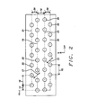
- Fig. 1 shows a top view of a standard integrated circuit board 10 having a number of ball/ pad regions 11.
- the pitch 12 is the same in the x and y directions and is determined by the number of required ball/pad regions and the target package size.
- manufacturing rules require a minimum pitch for a given manufacturing technology. As the density of circuits in integrated circuit chips increases and the size of the chips decreases more wiring channels are required. Smaller pitch is a serious limitation to the availability of sufficient wiring channels.
- ICs with a single outside row and/or column of balls/pads may be routed on a PCB (printed circuit board) using a single outer layer of metal.
- PCB printed circuit board
- the PCBs typically have to use multiple layers of metal.
- Inner rows/columns are then routed on the outside layer only towards a close placed via, which then allows a further signal routing inside a deeper PCB layer.
- Vias are drilled holes with a layer of copper at the circumference.
- Standard vias are mechanically drilled and have a typical minimum hole diameter of 200-300um. Because of mechanical tolerances the connected landing pads of standard vias are typically ⁇ 550um.
- a staggered ball/pad region pitch arrangement is used to achieve a reduced pitch in one direction while maintaining a minimum ball to ball (pad to pad) distance.
- a ball/pad region pitch of about 0.5 mm can be used in the x direction and a pitch of about 0.32 mm in the y direction with alternating rows locating balls/pads at the gaps of adjacent rows. This provides a spacing of about 0.4mm between nearest balls/pads in adjacent rows.
- a different ball/pad region pitch can be used in other regions of the integrated circuit package.
- the distance in the y direction between the centerline 21 of the ball/pad regions 22 in the top row and the centerline 19 of the ball/pad regions 22 in the next row and between the centerline 25 of the ball pad regions 22 bottom row and the centerline 23 of the ball/pad regions in the next to last row is a pitch of a second distance 20.
- the distance between the centerlines 19 and 23 of the ball/pad regions in the two middle rows is a pitch of a third distance 18.
- the distance between the ball/pad regions in the first row and the nearest neighbor ball/pad regions in the second row and between the ball/pad regions in the last row and the nearest neighbor ball/pad regions in the next to last row is a pitch of a fourth distance 17
- the first distance 16 is about 0.5mm
- the second distance 20 is about 0.32mm
- the third distance 18 is about 0.4mm.
- different values for the first, second, and third distances could be used which would result in a different fourth distance.
- the location of the left most ball/pad regions are on a reference line 15.
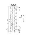
- Fig. 3 shows a top view of a printed circuit board of this invention showing four rows of an x-y grid for locating the ball/pad regions 22.
- the ball/pad regions 22 have a first pitch in the x direction of a first distance 24 for all four rows.
- the second row and bottom row have an off-set in the x direction of a second distance 33, which is one half of the first distance 24.
- the pitch of the centerlines of the ball/pad regions in the y direction have a second pitch of a second distance 30. This results in a separation between nearest neighbor ball/pad regions of a third distance 28.
- a first distance 24 of about 0.5 mm and a second distance 30 of about 0.32 mm results in a third distance 28 of about 0.41 mm.
- the location of the left most ball/pad regions are on a reference line 31.
- first distance 24 and second distance 30 can be used, which will provide a different third distance 28 for separation between nearest neighbor ball/pad regions.
- first distance 24 of 0.58 mm and a second distance 30 of 0.29 mm results in a third distance 28 of about 0.41 mm.
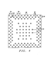
- Fig. 4 shows another embodiment of the ball/pad region layout of this invention.
- Fig. 4 shows a top view of a printed circuit board 37 having a ball/pad region layout as described in a previous paragraph and shown in Fig. 3 around the four edges of the printed circuit board.
- like reference numbers identify like features of the invention as described above and shown in Fig. 3 .
- Fig. 4 also shows ball/pad regions 35 on a more widely spaced grid at the center portion of the printed circuit board.
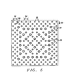
- Fig. 5 shows the printed circuit board of Fig. 4 also showing the placement of standard vias 35.
Landscapes
- Production Of Multi-Layered Print Wiring Board (AREA)
- Electric Connection Of Electric Components To Printed Circuits (AREA)
Priority Applications (2)
| Application Number | Priority Date | Filing Date | Title |
|---|---|---|---|
| EP11368010A EP2503594A1 (de) | 2011-03-21 | 2011-03-21 | Ball-/Padlayout einer integrierten Schaltungspackung mit optimiertem Signalrouting |
| US13/066,656 US20120241208A1 (en) | 2011-03-21 | 2011-04-20 | Signal routing Optimized IC package ball/pad layout |
Applications Claiming Priority (1)
| Application Number | Priority Date | Filing Date | Title |
|---|---|---|---|
| EP11368010A EP2503594A1 (de) | 2011-03-21 | 2011-03-21 | Ball-/Padlayout einer integrierten Schaltungspackung mit optimiertem Signalrouting |
Publications (1)
| Publication Number | Publication Date |
|---|---|
| EP2503594A1 true EP2503594A1 (de) | 2012-09-26 |
Family
ID=44118475
Family Applications (1)
| Application Number | Title | Priority Date | Filing Date |
|---|---|---|---|
| EP11368010A Withdrawn EP2503594A1 (de) | 2011-03-21 | 2011-03-21 | Ball-/Padlayout einer integrierten Schaltungspackung mit optimiertem Signalrouting |
Country Status (2)
| Country | Link |
|---|---|
| US (1) | US20120241208A1 (de) |
| EP (1) | EP2503594A1 (de) |
Families Citing this family (11)
| Publication number | Priority date | Publication date | Assignee | Title |
|---|---|---|---|---|
| US8988895B2 (en) * | 2011-08-23 | 2015-03-24 | Tessera, Inc. | Interconnection elements with encased interconnects |
| JP2015088539A (ja) * | 2013-10-29 | 2015-05-07 | 株式会社デンソー | 半導体パッケージ、および、これを実装する配線基板 |
| US10177107B2 (en) * | 2016-08-01 | 2019-01-08 | Xilinx, Inc. | Heterogeneous ball pattern package |
| US10937707B2 (en) * | 2017-02-22 | 2021-03-02 | Kyocera Corporation | Wiring substrate, electronic device, and electronic module |
| DE102017218273B4 (de) | 2017-10-12 | 2022-05-12 | Vitesco Technologies GmbH | Halbleiterbaugruppe |
| DE102017128568A1 (de) * | 2017-12-01 | 2019-06-06 | Infineon Technologies Ag | Halbleiterchip mit einer vielzahl von externen kontakten, chip-anordnung und verfahren zum überprüfen einer ausrichtung einer position eines halbleiterchips |
| WO2020043170A1 (en) * | 2018-08-31 | 2020-03-05 | Changxin Memory Technologies, Inc. | Arrangement of bond pads on an integrated circuit chip |
| CN109618489A (zh) * | 2018-12-29 | 2019-04-12 | 晶晨半导体(深圳)有限公司 | 印制电路板 |
| US11705378B2 (en) * | 2020-07-20 | 2023-07-18 | Taiwan Semiconductor Manufacturing Company, Ltd. | Semiconductor packages and methods of forming the same |
| KR20220057044A (ko) * | 2020-10-29 | 2022-05-09 | 에스케이하이닉스 주식회사 | 반도체 장치 |
| CN115767884B (zh) * | 2022-11-25 | 2026-02-06 | 维沃移动通信有限公司 | 电路板组件及电路板组件的制备方法 |
Citations (12)
| Publication number | Priority date | Publication date | Assignee | Title |
|---|---|---|---|---|
| US5567655A (en) | 1993-05-05 | 1996-10-22 | Lsi Logic Corporation | Method for forming interior bond pads having zig-zag linear arrangement |
| US5818114A (en) | 1995-05-26 | 1998-10-06 | Hewlett-Packard Company | Radially staggered bond pad arrangements for integrated circuit pad circuitry |
| US6057601A (en) | 1998-11-27 | 2000-05-02 | Express Packaging Systems, Inc. | Heat spreader with a placement recess and bottom saw-teeth for connection to ground planes on a thin two-sided single-core BGA substrate |
| US6168854B1 (en) | 1996-12-23 | 2001-01-02 | Nortel Networks Limited | Method of making a printed circuit board having a tin/lead coating |
| US6407462B1 (en) * | 2000-12-30 | 2002-06-18 | Lsi Logic Corporation | Irregular grid bond pad layout arrangement for a flip chip package |
| WO2003065451A1 (en) * | 2002-01-31 | 2003-08-07 | Thomson Licensing S.A. | Flip chip die bond pads, die bond pad placement and routing optimization |
| US6664483B2 (en) * | 2001-05-15 | 2003-12-16 | Intel Corporation | Electronic package with high density interconnect and associated methods |
| US6734545B1 (en) * | 1995-11-29 | 2004-05-11 | Hitachi, Ltd. | BGA type semiconductor device and electronic equipment using the same |
| US20050186769A1 (en) * | 2004-02-24 | 2005-08-25 | Young Dave W. | Hexagonal array structure for ball grid array packages |
| US7495296B2 (en) | 2004-06-01 | 2009-02-24 | Panasonic Corporation | Semiconductor integrated circuit device |
| US20090189158A1 (en) * | 2008-01-30 | 2009-07-30 | Kabushiki Kaisha Toshiba | Semiconductor device |
| US7652379B2 (en) | 2007-07-23 | 2010-01-26 | National Semiconductor Corporation | Bond pad stacks for ESD under pad and active under pad bonding |
Family Cites Families (10)
| Publication number | Priority date | Publication date | Assignee | Title |
|---|---|---|---|---|
| US6111756A (en) * | 1998-09-11 | 2000-08-29 | Fujitsu Limited | Universal multichip interconnect systems |
| US6815621B2 (en) * | 2000-10-02 | 2004-11-09 | Samsung Electronics Co., Ltd. | Chip scale package, printed circuit board, and method of designing a printed circuit board |
| US6556454B1 (en) * | 2000-10-31 | 2003-04-29 | Agilent Technologies, Inc. | High density contact arrangement |
| JP3785083B2 (ja) * | 2001-11-07 | 2006-06-14 | 株式会社東芝 | 半導体装置、電子カード及びパッド再配置基板 |
| US6768206B2 (en) * | 2002-05-07 | 2004-07-27 | Kabushiki Kaisha Toshiba | Organic substrate for flip chip bonding |
| US6919635B2 (en) * | 2003-11-04 | 2005-07-19 | International Business Machines Corporation | High density microvia substrate with high wireability |
| US7372169B2 (en) * | 2005-10-11 | 2008-05-13 | Via Technologies, Inc. | Arrangement of conductive pads on grid array package and on circuit board |
| JP5352146B2 (ja) * | 2008-07-23 | 2013-11-27 | ルネサスエレクトロニクス株式会社 | 半導体装置 |
| US9355951B2 (en) * | 2009-08-28 | 2016-05-31 | Marvell World Trade Ltd. | Interconnect layouts for electronic assemblies |
| JP5342422B2 (ja) * | 2009-12-10 | 2013-11-13 | ルネサスエレクトロニクス株式会社 | 半導体装置およびその製造方法 |
-
2011
- 2011-03-21 EP EP11368010A patent/EP2503594A1/de not_active Withdrawn
- 2011-04-20 US US13/066,656 patent/US20120241208A1/en not_active Abandoned
Patent Citations (12)
| Publication number | Priority date | Publication date | Assignee | Title |
|---|---|---|---|---|
| US5567655A (en) | 1993-05-05 | 1996-10-22 | Lsi Logic Corporation | Method for forming interior bond pads having zig-zag linear arrangement |
| US5818114A (en) | 1995-05-26 | 1998-10-06 | Hewlett-Packard Company | Radially staggered bond pad arrangements for integrated circuit pad circuitry |
| US6734545B1 (en) * | 1995-11-29 | 2004-05-11 | Hitachi, Ltd. | BGA type semiconductor device and electronic equipment using the same |
| US6168854B1 (en) | 1996-12-23 | 2001-01-02 | Nortel Networks Limited | Method of making a printed circuit board having a tin/lead coating |
| US6057601A (en) | 1998-11-27 | 2000-05-02 | Express Packaging Systems, Inc. | Heat spreader with a placement recess and bottom saw-teeth for connection to ground planes on a thin two-sided single-core BGA substrate |
| US6407462B1 (en) * | 2000-12-30 | 2002-06-18 | Lsi Logic Corporation | Irregular grid bond pad layout arrangement for a flip chip package |
| US6664483B2 (en) * | 2001-05-15 | 2003-12-16 | Intel Corporation | Electronic package with high density interconnect and associated methods |
| WO2003065451A1 (en) * | 2002-01-31 | 2003-08-07 | Thomson Licensing S.A. | Flip chip die bond pads, die bond pad placement and routing optimization |
| US20050186769A1 (en) * | 2004-02-24 | 2005-08-25 | Young Dave W. | Hexagonal array structure for ball grid array packages |
| US7495296B2 (en) | 2004-06-01 | 2009-02-24 | Panasonic Corporation | Semiconductor integrated circuit device |
| US7652379B2 (en) | 2007-07-23 | 2010-01-26 | National Semiconductor Corporation | Bond pad stacks for ESD under pad and active under pad bonding |
| US20090189158A1 (en) * | 2008-01-30 | 2009-07-30 | Kabushiki Kaisha Toshiba | Semiconductor device |
Also Published As
| Publication number | Publication date |
|---|---|
| US20120241208A1 (en) | 2012-09-27 |
Similar Documents
| Publication | Publication Date | Title |
|---|---|---|
| EP2503594A1 (de) | Ball-/Padlayout einer integrierten Schaltungspackung mit optimiertem Signalrouting | |
| KR101218011B1 (ko) | 플립 칩 인터커넥션 패드 레이아웃 반도체 패키지 및 그 생산 방법 | |
| EP1705967B1 (de) | Glättungskapazität ausserhalb des Rasters von BGA Bauelementen und Verfahren zu deren Herstellung | |
| JP2003007750A (ja) | 半導体装置 | |
| JP2003188508A (ja) | プリント配線板、面実装形回路部品および回路モジュール | |
| JPH10335532A (ja) | 多層回路基板 | |
| US11369020B2 (en) | Stacked transmission line | |
| US6664620B2 (en) | Integrated circuit die and/or package having a variable pitch contact array for maximization of number of signal lines per routing layer | |
| CN1203546C (zh) | 有机芯片载体的高密度设计 | |
| KR100967565B1 (ko) | 반도체 부품 | |
| JP3730625B2 (ja) | フリップチップボンディングのための有機基板 | |
| US7161812B1 (en) | System for arraying surface mount grid array contact pads to optimize trace escape routing for a printed circuit board | |
| US20090065935A1 (en) | Systems and methods for ball grid array (bga) escape routing | |
| JP2005166794A (ja) | 部品パッケージとプリント配線基板および電子機器 | |
| EP1714530B1 (de) | Verfahren zur vergrösserung einer routing-dichte für eine leiterplatte und eine solche leiterplatte | |
| US20090174072A1 (en) | Semiconductor system having bga package with radially ball-depopulated substrate zones and board with radial via zones | |
| JP3994312B2 (ja) | プリント配線板およびその製造方法およびインターポーザ基板 | |
| US8013253B2 (en) | Electrical connection board and assembly of such a board and a semiconductor component comprising an integrated circuit chip | |
| JP3008887U (ja) | Icピッチ変換基板 | |
| JP2009164294A (ja) | 多層回路基板および半導体装置 | |
| JPH11260955A (ja) | 多層回路基板 | |
| US20070114578A1 (en) | Layout structure of ball grid array | |
| JP2005228776A (ja) | 配線方法および配線基板 | |
| JP2005005601A (ja) | 印刷回路配線板の配線レイアウト構造 |
Legal Events
| Date | Code | Title | Description |
|---|---|---|---|
| PUAI | Public reference made under article 153(3) epc to a published international application that has entered the european phase |
Free format text: ORIGINAL CODE: 0009012 |
|
| AK | Designated contracting states |
Kind code of ref document: A1 Designated state(s): AL AT BE BG CH CY CZ DE DK EE ES FI FR GB GR HR HU IE IS IT LI LT LU LV MC MK MT NL NO PL PT RO RS SE SI SK SM TR |
|
| AX | Request for extension of the european patent |
Extension state: BA ME |
|
| 17P | Request for examination filed |
Effective date: 20130326 |
|
| 17Q | First examination report despatched |
Effective date: 20140214 |
|
| STAA | Information on the status of an ep patent application or granted ep patent |
Free format text: STATUS: THE APPLICATION IS DEEMED TO BE WITHDRAWN |
|
| 18D | Application deemed to be withdrawn |
Effective date: 20161001 |