EP2502289B1 - Method for making material useful in optoelectronic device, the material and the optoelectronic device - Google Patents
Method for making material useful in optoelectronic device, the material and the optoelectronic device Download PDFInfo
- Publication number
- EP2502289B1 EP2502289B1 EP10785248.5A EP10785248A EP2502289B1 EP 2502289 B1 EP2502289 B1 EP 2502289B1 EP 10785248 A EP10785248 A EP 10785248A EP 2502289 B1 EP2502289 B1 EP 2502289B1
- Authority
- EP
- European Patent Office
- Prior art keywords
- radical
- layer
- groups
- compound
- aromatic
- Prior art date
- Legal status (The legal status is an assumption and is not a legal conclusion. Google has not performed a legal analysis and makes no representation as to the accuracy of the status listed.)
- Active
Links
- 0 C*(C)c1ccc(C)cc1 Chemical compound C*(C)c1ccc(C)cc1 0.000 description 3
- IWDCLRJOBJJRNH-UHFFFAOYSA-N Cc(cc1)ccc1O Chemical compound Cc(cc1)ccc1O IWDCLRJOBJJRNH-UHFFFAOYSA-N 0.000 description 1
Images
Classifications
-
- H—ELECTRICITY
- H10—SEMICONDUCTOR DEVICES; ELECTRIC SOLID-STATE DEVICES NOT OTHERWISE PROVIDED FOR
- H10K—ORGANIC ELECTRIC SOLID-STATE DEVICES
- H10K85/00—Organic materials used in the body or electrodes of devices covered by this subclass
- H10K85/10—Organic polymers or oligomers
- H10K85/111—Organic polymers or oligomers comprising aromatic, heteroaromatic, or aryl chains, e.g. polyaniline, polyphenylene or polyphenylene vinylene
-
- C—CHEMISTRY; METALLURGY
- C08—ORGANIC MACROMOLECULAR COMPOUNDS; THEIR PREPARATION OR CHEMICAL WORKING-UP; COMPOSITIONS BASED THEREON
- C08G—MACROMOLECULAR COMPOUNDS OBTAINED OTHERWISE THAN BY REACTIONS ONLY INVOLVING UNSATURATED CARBON-TO-CARBON BONDS
- C08G73/00—Macromolecular compounds obtained by reactions forming a linkage containing nitrogen with or without oxygen or carbon in the main chain of the macromolecule, not provided for in groups C08G12/00 - C08G71/00
- C08G73/02—Polyamines
- C08G73/026—Wholly aromatic polyamines
-
- C—CHEMISTRY; METALLURGY
- C08—ORGANIC MACROMOLECULAR COMPOUNDS; THEIR PREPARATION OR CHEMICAL WORKING-UP; COMPOSITIONS BASED THEREON
- C08K—Use of inorganic or non-macromolecular organic substances as compounding ingredients
- C08K5/00—Use of organic ingredients
- C08K5/0008—Organic ingredients according to more than one of the "one dot" groups of C08K5/01 - C08K5/59
- C08K5/0025—Crosslinking or vulcanising agents; including accelerators
-
- H—ELECTRICITY
- H10—SEMICONDUCTOR DEVICES; ELECTRIC SOLID-STATE DEVICES NOT OTHERWISE PROVIDED FOR
- H10K—ORGANIC ELECTRIC SOLID-STATE DEVICES
- H10K50/00—Organic light-emitting devices
- H10K50/10—OLEDs or polymer light-emitting diodes [PLED]
- H10K50/14—Carrier transporting layers
- H10K50/15—Hole transporting layers
- H10K50/155—Hole transporting layers comprising dopants
Definitions
- the invention relates generally to methods for making materials useful, e.g., as hole-transport materials and/or electron-block materials of optoelectronic devices, the materials and the optoelectronic devices comprising the materials.
- Optoelectronic devices e.g. Organic Light Emitting Devices (OLEDs), which make use of thin film materials that emit light when subjected to a voltage bias, are expected to become an increasingly popular form of flat panel display technology.
- OLEDs have a wide variety of potential applications, including cell phones, personal digital assistants (PDAs), computer displays, informational displays in vehicles, television monitors, as well as light sources for general illumination. Due to their bright colors, wide viewing angle, compatibility with full motion video, broad temperature ranges, thin and conformable form factor, low power requirements and the potential for low cost manufacturing processes, OLEDs are seen as a future replacement technology for cathode ray tubes (CRTs) and liquid crystal displays (LCDs). Due to their high luminous efficiencies, OLEDs are seen as having the potential to replace incandescent, and perhaps even fluorescent, lamps for certain types of applications.
- CTRs cathode ray tubes
- LCDs liquid crystal displays
- OLEDs possess a sandwiched structure, which consists of one or more organic layers between two opposite electrodes.
- multi-layered devices usually comprise at least three layers: a hole injection/transport layer, an emissive layer and an electron transport layer (ETL).
- the hole injection/transport layer serves as an electron blocking layer and the ETL as a hole blocking layer.
- Single-layered OLEDs comprise only one layer of materials between two opposite electrodes.
- WO-A-98/06773 concerns poly(arylamines) and films thereof formed in electrophotographic and electroluminescent devices and in polymeric light emitting diodes. Relatively small amounts of the polymers may be used to form the films, which are relatively high molecular weight charge transport compounds.
- WO-A-2006/043681 WO-A-2006/043687 and EP-A-2 333 862 also disclose relevant compositions.
- the present invention provides a method for making a material as defined in appended claim 1.
- the invention relates to a method for making a material, comprising: providing a mixture of a polytriarylamine and a compound; forming a film of the mixture; and treating the film; wherein the compound comprises at least one functional group selected from arylamine and arylphosphine and at least two functional groups selected from vinyl, allyl, vinyl ether, epoxy, and acrylate.
- the invention relates to a material made by the above method.
- the invention relates to an optoelectronic device comprising the above material.
- the invention relates to a method for making an optoelectronic device, comprising: providing an electrode; providing a light emission layer; and providing between the electrode and the light emission layer a hole-transport layer comprising a material made by the above method.
- the mixture is a mixture solution of the polytriaylamine and the compound.
- the treating comprises treating the film under heat and/or photo radiation.
- the method further comprises rinsing the treated film.
- the polytriarylamine comprises structural unit of formula I wherein R 1 is, independently at each occurrence, a C 1 -C 20 aliphatic radical, a C 3 -C 20 aromatic radical, or a C 3 -C 20 cycloaliphatic radical; and a is, independently at each occurrence, an integer ranging from 0-4.
- the polytriarylamine comprises structural unit of formula II
- the compound is of formula: wherein
- the compound is selected from: and
- the polytriarylamine and the compound is 1:1 in weight ratio in the mixture solution.
- OLEDs organic light emitting devices
- An optoelectronic device typically includes in the simplest case, an anode layer and a corresponding cathode layer with an organic electroluminescent layer disposed between said anode and said cathode.
- an OLED typically includes in the simplest case, an anode layer and a corresponding cathode layer with an organic electroluminescent layer disposed between said anode and said cathode.
- a voltage bias is applied across the electrodes, electrons are injected by the cathode into the electroluminescent layer while electrons are removed from (or "holes" are “injected” into) the electroluminescent layer from the anode.
- Light emission occurs as holes combine with electrons within the electroluminescent layer to form singlet or triplet excitons, light emission occurring as singlet and/or triplet excitons decay to their ground states via radiative decay.
- Other components which may be present in an OLED in addition to the anode, cathode and light emitting material include a hole injection layer, an electron injection layer, and an electron transport layer.
- the electron transport layer need not be in direct contact with the cathode, and frequently the electron transport layer also serves as a hole blocking layer to prevent holes migrating toward the cathode.
- Additional components which may be present in an organic light-emitting device include hole transporting layers, hole transporting emission (emitting) layers and electron transporting emission (emitting) layers.
- the OLEDs comprising the materials of the invention may be a fluorescent OLED comprising a singlet emitter.
- the OLEDs comprising the materials of the invention may be a phosphorescent OLED comprising at least one triplet emitter.
- the OLEDs comprising the polymers of the invention comprise at least one singlet emitter and at least one triplet emitter.
- the OLEDs comprising the materials of the invention may contain one or more, any or a combination of blue, yellow, orange, red phosphorescent dyes, including complexes of transition metals such as Ir, Os and Pt.
- electrophosphorescent and electrofluorescent metal complexes such as those supplied by American Dye Source, Inc., Quebec, Canada may be used.
- the materials may be part of an emissive layer, or hole transporting layer or electron transporting layer, or electron injection layer of an OLED or any combination thereof.
- the organic electroluminescent layer i.e., the emissive layer or light emission layer, is a layer within an organic light emitting device which when in operation contains a significant concentration of both electrons and holes and provides sites for exciton formation and light emission.
- a hole injection layer is a layer in contact with the anode which promotes the injection of holes from the anode into the interior layers of the OLED: and an electron injection layer is a layer in contact with the cathode that promotes the injection of electrons from the cathode into the OLED; an electron transport layer is a layer which facilitates conduction of electrons from the cathode and/or the electron injection layer to a charge recombination site.
- a hole transporting layer is a layer which when the OLED is in operation facilitates conduction of holes from the anode and/or the hole injection layer to charge recombination sites and which need not be in direct contact with the anode.
- a hole transporting emission layer is a layer in which when the OLED is in operation facilitates the conduction of holes to charge recombination sites, and in which the majority of charge carriers are holes, and in which emission occurs not only through recombination with residual electrons, but also through the transfer of energy from a charge recombination zone elsewhere in the device.
- An electron transporting emission layer is a layer in which when the OLED is in operation facilitates the conduction of electrons to charge recombination sites, and in which the majority of charge carriers are electrons, and in which emission occurs not only through recombination with residual holes, but also through the transfer of energy from a charge recombination zone elsewhere in the device.
- Materials suitable for use as the anode includes materials having a bulk resistivity of preferred about 1000 ohms per square, as measured by a four-point probe technique.
- Indium tin oxide (ITO) is frequently used as the anode because it is substantially transparent to light transmission and thus facilitates the escape of light emitted from electro-active organic layer.
- Other materials, which may be utilized as the anode layer include tin oxide, indium oxide, zinc oxide, indium zinc oxide, zinc indium tin oxide, antimony oxide, and mixtures thereof.
- Materials suitable for use as the cathode include general electrical conductors including, but not limited to metals and metal oxides such as ITO etc which can inject negative charge carriers (electrons) into the inner layer(s) of the OLED.
- Various metals suitable for use as the cathode include K, Li, Na, Cs, Mg, Ca, Sr, Ba, Al, Ag, Au, In, Sn, Zn, Zr, Sc, Y, elements of the lanthanide series, alloys thereof, and mixtures thereof.
- Suitable alloy materials for use as the cathode layer include Ag-Mg, Al-Li, In-Mg, Al-Ca, and Al-Au alloys.
- Layered non-alloy structures may also be employed in the cathode, such as a thin layer of a metal such as calcium, or a metal fluoride, such as LiF, covered by a thicker layer of a metal, such as aluminum or silver.
- the cathode may be composed of a single metal, and especially of aluminum metal.
- Materials suitable for use in electron transport layers include poly(9,9-dioctyl fluorene), tris(8-hydroxyquinolato) aluminum (Alq3), 2,9-dimethyl-4,7-diphen-1,1-phenanthroline, 4,7-diphenyl-1,10-phenanthroline, 2-(4-biphenylyl)-5-(4-t-butylphenyl)-1,3,4-oxadiazole, 3-(4-biphenylyl)-4-phenyl-5-(4-t-butylphenyl)-1,2,4- triazole, 1,3,4-oxadiazole-containing polymers, 1,3,4-triazole-containing polymers, quinoxaline-containing polymers, and cyano-PPV.
- Materials made herein may be used in hole transporting layers in place of, or in addition to traditional materials such as 1,1-bis((di-4-tolylamino) phenyl)cyclohexane, N,N'- bis(4-methylphenyl)-N,N'-bis(4-ethylphenyl)-(1,1'-(3,3'-dimethyl)biphenyl)-4,4'-diamine, tetrakis-(3-methylphenyl)-N,N,N',N'-2,5-phenylenediamine, phenyl-4-N,N-diphenylaminostyrene, p-(diethylamino) benzaldehyde diphenylhydrazone, triphenylamine, 1-phenyl-3-(p-(diethylamino)styryl)-5-(p-(diethylamino)phenyl)pyrazoline, 1,2-trans-bis(9H-
- Materials suitable for use in the light emitting layer include electroluminescent polymers such as polyfluorenes, preferably poly(9,9-dioctyl fluorene) and copolymers thereof, such as poly(9,9'-dioctylfluorene-co-bis-N,N'-(4-bulylphenyl)diphenylamine) (F8-TFB); poly(vinylcarbazole) and polyphenylenevinylene and their derivatives.
- the light emitting layer may include a blue, yellow, orange, green or red phosphorescent dye or metal complex, or a combination thereof.
- Materials suitable for use as the phosphorescent dye include, but are not limited to, tris(1-phenylisoquinoline) iridium (III) (red dye), tris(2-phenylpyridine) iridium (green dye) and Iridium (III) bis(2-(4,6-difluorephenyl)pyridinato-N,C2) (blue dye).
- commercially available electrofluorescent and electrophosphorescent metal complexes from ADS may also be used.
- ADS green dyes include ADS060GE, ADS061GE, ADS063GE, and ADS066GE, ADS078GE, and ADS090GE.
- ADS blue dyes include ADS064BE, ADS065BE, and ADS070BE.
- ADS red dyes include ADS067RE, ADS068RE, ADS069RE, ADS075RE, ADS076RE, ADS067RE, and ADS077RE.
- Materials made herein may form part of the hole-transport layer or hole injection layer or light emissive layer of optoelectronic devices, e.g., OLEDs.
- the OLEDs may be phosphorescent containing one or more, any or a combination of, blue, yellow, orange, green, red phosphorescent dyes.
- aromatic radical refers to an array of atoms having a valence of at least one comprising at least one aromatic group.
- the array of atoms having a valence of at least one comprising at least one aromatic group may include heteroatoms such as nitrogen, sulfur, selenium, silicon and oxygen, or may be composed exclusively of carbon and hydrogen.
- aromatic radical includes but is not limited to phenyl, pyridyl, furanyl, thienyl, naphthyl, phenylene, and biphenyl radicals.
- the aromatic radical contains at least one aromatic group.
- the aromatic radical may also include nonaromatic components.
- a benzyl group is an aromatic radical which comprises a phenyl ring (the aromatic group) and a methylene group (the nonaromatic component).
- a tetrahydronaphthyl radical is an aromatic radical comprising an aromatic group (C 6 H 3 ) fused to a nonaromatic component -(CH 2 ) 4 -.
- aromatic radical is defined herein to encompass a wide range of functional groups such as alkyl groups, alkenyl groups, alkynyl groups, haloalkyl groups, haloaromatic groups, conjugated dienyl groups, alcohol groups, ether groups, aldehydes groups, ketone groups, carboxylic acid groups, acyl groups (for example carboxylic acid derivatives such as esters and amides), amine groups, nitro groups, and the like.
- the 4-methylphenyl radical is a C 7 aromatic radical comprising a methyl group, the methyl group being a functional group which is an alkyl group.
- the 2-nitrophenyl group is a C6 aromatic radical comprising a nitro group, the nitro group being a functional group.
- Aromatic radicals include halogenated aromatic radicals such as 4-trifluoromethylphenyl, hexafluoroisopropylidenebis(4-phen-1-yloxy) (i.e., -OPhC(CF 3 ) 2 PhO-), 4-chloromethylphen-1-yl, 3-trifluorovinyl-2-thienyl, 3-trichloromethylphen-1-yl (i.e., 3-CCl 3 Ph-), 4-(3-bromoprop-1-yl)phen-1-yl (i.e., 4-BrCH 2 CH 2 CH 2 Ph-), and the like.
- halogenated aromatic radicals such as 4-trifluoromethylphenyl, hexafluoroisopropylidenebis(4-phen-1-yloxy) (i.e., -OPhC(CF 3 ) 2 PhO-), 4-chloromethylphen-1-yl, 3-trifluorovinyl-2-thienyl, 3-trich
- aromatic radicals include 4-allyloxyphen-1-oxy, 4-aminophen-1-yl (i.e., 4-H 2 NPh-), 3-aminocarbonylphen-1-yl (i.e., NH 2 COPh-), 4-benzoylphen-1-yl, dicyanomethylidenebis(4-phen-1-yloxy) (i.e., -OPhC(CN) 2 PhO-), 3-methylphen-1-yl, methylenebis(4-phen-1-yloxy) (i.e.,-OPhCH 2 PhO-), 2-ethylphen-1-yl, phenylethenyl, 3-formyl-2-thienyl, 2-hexyl-5-furanyl, hexamethylene-1,6-bis(4-phen-1-yloxy) (i.e., -OPh(CH 2 ) 6 PhO-), 4-hydroxymethylphen-t-yl (i.e., 4-HOCH 2 Ph-), 4-mer
- a C 3 - C 20 aromatic radical includes aromatic radicals containing at least three but no more than 20 carbon atoms.
- the aromatic radical 1-imidazolyl (C 3 H 2 N 2 -) represents a C 3 aromatic radical.
- the benzyl radical (C 7 H 7 -) represents a C 7 aromatic radical.
- cycloaliphatic radical refers to a radical having a valence of at least one, and comprising an array of atoms which is cyclic but which is not aromatic. As defined herein a “cycloaliphatic radical” does not contain an aromatic group.
- a "cycloaliphatic radical” may comprise one or more noncyclic components.
- a cyclohexylmethyl group (C 6 H 11 CH 2 -) is an cycloaliphatic radical which comprises a cyclohexyl ring (the array of atoms which is cyclic but which is not aromatic) and a methylene group (the noncyclic component).
- the cycloaliphatic radical may include heteroatoms such as nitrogen, sulfur, selenium, silicon and oxygen, or may be composed exclusively of carbon and hydrogen.
- cycloaliphatic radical is defined herein to encompass a wide range of functional groups such as alkyl groups, alkenyl groups, alkynyl groups, haloalkyl groups, conjugated dienyl groups, alcohol groups, ether groups, aldehyde groups, ketone groups, carboxylic acid groups, acyl groups (for example carboxylic acid derivatives such as esters and amides), amine groups, nitro groups, and the like.
- the 4-methylcyclopent-1-yl radical is a C 6 cycloaliphatic radical comprising a methyl group, the methyl group being a functional group which is an alkyl group.
- the 2-nitrocyclobut-1-yl radical is a C 4 cycloaliphatic radical comprising a nitro group, the nitro group being a functional group.
- a cycloaliphatic radical may comprise one or more halogen atoms which may be the same or different. Halogen atoms include, for example; fluorine, chlorine, bromine, and iodine.
- Cycloaliphatic radicals comprising one or more halogen atoms include 2-trifluoromethylcyclohex-1-yl, 4-bromodifluoromethylcyclooct-1-yl, 2-chlorodifluoromethylcyclohex-1-yl, hexafluoroisopropylidene-2,2-bis (cyclohex-4-yl) (i.e., -C 6 H 10 C(CF 3 ) 2 C 6 H 10 -), 2-chloromethycyclohex-1-yl, 3-difluoromethylenecyclohex-1-yl, 4-trichloromethylcyclohex-1-yloxy, 4-bromodichloromethylcyclohex-1-ylthio, 2-bromoethylcyclopent-1-yl, 2-bromopropylcyclohex-1-yloxy (e.g.
- cycloaliphatic radicals include 4-allyloxycyclohex-1-yl, 4-aminocyclohex-1-yl (i.e., H 2 NC 6 H 10 -), 4-aminocarbonylcyclopent-1-yl (i.e., NH 2 COC 5 H 8 -), 4-acetyloxycyclohex-1-yl, 2,2-dicyanoisopropylidenebis(cyclohex-4-yloxy) (i.e., -OC 6 H 10 C(CN) 2 C 6 H 10 O-), 3-methylcyclohex-1-yl, methylenebis(cyclohex-4-yloxy) (i.e., -OC 6 H 10 OCH 2 C 6 H 10 O-), 1-ethylcyclobut-1-yl, cyclopropylethenyl, 3-formyl-2-terahydrofuranyl, 2-hexyl
- a C 3 - C 10 cycloaliphatic radical includes cycloaliphatic radicals containing at least three but no more than 10 carbon atoms.
- the cycloaliphatic radical 2-tetrahydrofuranyl (C 4 H 7 O-) represents a C 4 cycloaliphatic radical.
- the cyclohexylmethyl radical (C 6 H 11 CH 2 -) represents a C 7 cycloaliphatic radical.
- aliphatic radical refers to an organic radical having a valence of at least one consisting of a linear or branched array of atoms which is not cyclic. Aliphatic radicals are defined to comprise at least one carbon atom. The array of atoms comprising the aliphatic radical may include heteroatoms such as nitrogen, sulfur, silicon, selenium and oxygen or may be composed exclusively of carbon and hydrogen.
- aliphatic radical is defined herein to encompass, as part of the "linear or branched array of atoms which is not cyclic organic radicals substituted with a wide range of functional groups such as alkyl groups, alkenyl groups, alkynyl groups, haloalkyl groups, conjugated dienyl groups, alcohol groups, ether groups, aldehyde groups, ketone groups, carboxylic acid groups, acyl groups (for example carboxylic acid derivatives such as esters and amides), amine groups, nitro groups, and the like.
- functional groups such as alkyl groups, alkenyl groups, alkynyl groups, haloalkyl groups, conjugated dienyl groups, alcohol groups, ether groups, aldehyde groups, ketone groups, carboxylic acid groups, acyl groups (for example carboxylic acid derivatives such as esters and amides), amine groups, nitro groups, and the like.
- the 4-methylpent-1-yl radical is a C 6 aliphatic radical comprising a methyl group, the methyl group being a functional group which is an alkyl group.
- the 4-nitrobut-1-yl group is a C 4 aliphatic radical comprising a nitro group, the nitro group being a functional group.
- An aliphatic radical may be a haloalkyl group which comprises one or more halogen atoms which may be the same or different. Halogen atoms include, for example; fluorine, chlorine, bromine, and iodine.
- Aliphatic radicals comprising one or more halogen atoms include the alkyl halides trifluoromethyl, bromodifluoromethyl, chlorodifluoromethyl, hexafluoroisopropylidene, chloromethyl, difluorovinylidene, trichloromethyl, bromodichloromethyl, bromoethyl, 2-bromotrimethylene (e.g. - CH 2 CHBrCH 2 -), and the like.
- aliphatic radicals include allyl, aminocarbonyl (i.e., -CONH 2 ), carboxyl, 2,2-dicyanoisopropylidene (i.e., - CH 2 C(CN) 2 CH 2 -), methyl (i.e., -CH 3 ), methylene (i.e., -CH 2 -), ethyl, ethylene, formyl (i.e.-CHO), hexyl, hexamethylene, hydroxymethyl (i.e.
- -CH 2 OH mercaptomethyl
- -CH 2 SH mercaptomethyl
- methylthio i.e., -SCH 3
- methylthiomethyl i.e., -CH 2 SCH 3
- methoxy, methoxycarbonyl i.e., CH 3 OCO-
- nitromethyl i.e., -CH 2 NO 2
- thiocarbonyl trimethylsilyl (i.e., (CH 3 ) 3 Si-), t-butyldimethylsilyl, 3-trimethyoxysilypropyl (i.e., (CH 3 O) 3 SiCH 2 CH 2 CH 2 -), vinyl, vinylidene, and the like.
- a C 1 - C 20 aliphatic radical contains at least one but no more than 20 carbon atoms.
- a methyl group i.e., CH 3 -
- a decyl group i.e., CH 3 (CH 2 ) 9 -
- CH 3 (CH 2 ) 9 - is an example of a C 10 aliphatic radical.
- heteroaryl refers to aromatic or unsaturated rings in which one or more carbon atoms of the aromatic ring(s) are replaced by a heteroatom(s) such as nitrogen, oxygen, boron, selenium, phosphorus, silicon or sulfur.
- Heteroaryl refers to structures that may be a single aromatic ring, multiple aromatic ring(s), or one or more aromatic rings coupled to one or more non-aromatic ring(s). In structures having multiple rings, the rings can be fused together, linked covalently, or linked to a common group such as an ether, methylene or ethylene moiety.
- the common linking group may also be a carbonyl as in phenol pyridyl ketone.
- heteroaryl rings include thiophene, pyridine, isoxazole, pyrazole, pyrrole, furan, imidazole, indole, thiazole, benzimidazole, quinoline, isoquinoline, quinoxaline, pyrimidine, pyrazine, tetrarole, triazole, benzo-fused analogues of these groups, benzopyranone, phenylpyridine, tolylpyridine, benzothienylpyridine, phenylisoquinoline, dibenzoquinozaline, fluorenylpyridine, ketopyrrole, 2-phenylbenzoxazole, 2 phenylbenzothiazole, thienylpyridine, benzothienylpyridine, 3 methoxy-2-phenylpyridine, phenylimine, pyridylnaphthalene, pyridylpyrrole, pyridylimidazole, and
- aryl is used herein to refer to an aromatic substituent which may be single aromatic ring or multiple aromatic rings which are fused together, linked covalently, or linked to a common group such as an ether, methylene or ethylene moiety.
- the aromatic ring(s) may include phenyl, naphthyl, anthracenyl, and biphenyl, among others.
- aryls have between 1 and 200 carbon atoms, between 1 and 50 carbon atoms or between 1 and 20 carbon atoms.
- alkyl is used herein to refer to a branched or unbranched, saturated or unsaturated acyclic hydrocarbon radical. Suitable alkyl radicals include, for example, methyl, ethyl, n-propyl, i-propyl, 2-propenyl (or allyl), vinyl, n-butyl, t-butyl, i-butyl (or 2-methylpropyl), etc. In particular embodiments, alkyls have between I and 200 carbon atoms, between 1 and 50 carbon atoms or between 1 and 20 carbon atoms.
- cycloalkyl is used herein to refer to a saturated or unsaturated cyclic non-aromatic hydrocarbon radical having a single ring or multiple condensed rings.
- Suitable cycloalkyl radicals include, for example, cyclopentyl, cyclohexyl, cyclooctenyl, bicyclooctyl, etc.
- cycloalkyls have between 3 and 200 carbon atoms, between 3 and 50 carbon atoms or between 3 and 20 carbon atoms.
- any numerical values recited herein include all values from the lower value to the upper value in increments of one unit provided that there is a separation of at least 2 units between any lower value and any higher value.
- the amount of a component or a value of a process variable such as, for example, temperature, pressure, time and the like is, for example, from 1 to 90, preferably from 20 to 80, more preferably from 30 to 70, it is intended that values such as 15 to 85, 22 to 68, 43 to 51, 30 to 32 etc. are expressly enumerated in this specification.
- one unit is considered to be 0.0001, 0.001, 0.01 or 0.1 as appropriate.
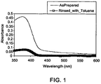
- ADS254 was purchased from American Dye Sources, Inc. and used as received. A 0.5 w/v% solution of ADS254 was prepared by dissolving 10 mg of ADS254 in 2.0 ml toluene. A thin film (30 nm in thickness) of ADS254 was then obtained by spin-casting the solution atop a pre-cleaned quartz substrate, and baked at 170°C to remove residual solvent. A UV-vis absorption spectrometer was then used to record the absorbance of the film. Then the sample was rinsed with toluene by spin-casting toluene atop the film. Another UV-vis spectrum was taken.
- absorbance intensity peaking at 380 nm decreased from 0.293 for the sample as prepared to 0.04 upon rinsing with toluene, indicating that nearly 85% of ADS254 got washed off by toluene.
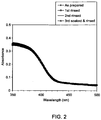
- Compound 1 was obtained from Konica Minolta Holdings, Inc., Tokyo, Japan. The experiment was conducted in a way similar to the comparative Example 1.
- a mixture solution of ADS254:compound 1 (50:50) was prepared by mixing 0.8 ml of 0.5 w/v% ADS254 in toluene and 0.8 ml of 0.5 w/v% compound 1 in toluene.
- a thin film (35 nm in thickness) of ADS254:compound 1 was then obtained by spin-casting, which was baked at 165°C for 10 seconds and cured under UV (365 nm & 20 mW/cm2) for 30 seconds, further baked at 130 °C for 20 minutes.
Landscapes
- Chemical & Material Sciences (AREA)
- Health & Medical Sciences (AREA)
- Chemical Kinetics & Catalysis (AREA)
- Medicinal Chemistry (AREA)
- Polymers & Plastics (AREA)
- Organic Chemistry (AREA)
- Engineering & Computer Science (AREA)
- Materials Engineering (AREA)
- Electroluminescent Light Sources (AREA)
- Polymerisation Methods In General (AREA)
- Graft Or Block Polymers (AREA)
Applications Claiming Priority (2)
| Application Number | Priority Date | Filing Date | Title |
|---|---|---|---|
| US12/619,740 US8455042B2 (en) | 2009-11-17 | 2009-11-17 | Method for making material useful in optoelectronic device, the material and the optoelectronic device |
| PCT/US2010/055948 WO2011062802A1 (en) | 2009-11-17 | 2010-11-09 | Method for making material useful in optoelectronic device, the material and the optoelectronic device |
Publications (2)
| Publication Number | Publication Date |
|---|---|
| EP2502289A1 EP2502289A1 (en) | 2012-09-26 |
| EP2502289B1 true EP2502289B1 (en) | 2016-04-06 |
Family
ID=43479481
Family Applications (1)
| Application Number | Title | Priority Date | Filing Date |
|---|---|---|---|
| EP10785248.5A Active EP2502289B1 (en) | 2009-11-17 | 2010-11-09 | Method for making material useful in optoelectronic device, the material and the optoelectronic device |
Country Status (7)
| Country | Link |
|---|---|
| US (1) | US8455042B2 (enExample) |
| EP (1) | EP2502289B1 (enExample) |
| JP (1) | JP5716035B2 (enExample) |
| KR (1) | KR101776972B1 (enExample) |
| CN (1) | CN102725875B (enExample) |
| TW (1) | TWI498353B (enExample) |
| WO (1) | WO2011062802A1 (enExample) |
Families Citing this family (11)
| Publication number | Priority date | Publication date | Assignee | Title |
|---|---|---|---|---|
| US20110077373A1 (en) * | 2009-09-29 | 2011-03-31 | General Electric Company | Polymer and optoelectronic device comprising the same |
| US20120049168A1 (en) * | 2010-08-31 | 2012-03-01 | Universal Display Corporation | Cross-Linked Charge Transport Layer Containing an Additive Compound |
| US9397294B2 (en) * | 2011-07-05 | 2016-07-19 | Solvay Usa, Inc. | Vertically phase-separating semiconducting organic material layers |
| WO2013080696A1 (ja) * | 2011-11-29 | 2013-06-06 | コニカミノルタ株式会社 | 有機el素子 |
| EP2838931A1 (de) | 2012-04-17 | 2015-02-25 | Merck Patent GmbH | Vernetzbare sowie vernetzte polymere, verfahren zu deren herstellung sowie deren verwendung |
| KR101382292B1 (ko) | 2012-09-21 | 2014-04-08 | 현대자동차(주) | 플라이휠의 댐핑장치 |
| WO2016026123A1 (en) | 2014-08-21 | 2016-02-25 | Dow Global Technologies Llc | Compositions comprising oxygen substituted benzocyclobutenes and dienophiles, and electronic devices containing same |
| TWI657123B (zh) * | 2016-01-27 | 2019-04-21 | 國立交通大學 | 鈣鈦礦型發光元件及其製造方法 |
| JP2019518845A (ja) * | 2016-06-28 | 2019-07-04 | ダウ グローバル テクノロジーズ エルエルシー | 有機電荷輸送膜を作製するためのプロセス |
| CN106449999A (zh) * | 2016-09-21 | 2017-02-22 | 广西南宁荣威德新能源科技有限公司 | 一种新型环保宽光谱太阳能电池材料 |
| CN109585698B (zh) * | 2018-11-12 | 2020-11-27 | 天津理工大学 | 一种溶液法制备p-i-n结构的低压驱动有机发光二极管的方法 |
Family Cites Families (20)
| Publication number | Priority date | Publication date | Assignee | Title |
|---|---|---|---|---|
| US5728801A (en) | 1996-08-13 | 1998-03-17 | The Dow Chemical Company | Poly (arylamines) and films thereof |
| JPH10338872A (ja) | 1997-06-09 | 1998-12-22 | Tdk Corp | 色変換材料およびこれを用いた有機elカラーディスプレイ |
| US6572985B2 (en) * | 2000-12-15 | 2003-06-03 | Shuang Xie Light Corporation | Electroluminescent compositions and devices |
| TW200300154A (en) * | 2001-11-09 | 2003-05-16 | Jsr Corp | Light emitting polymer composition, and organic electroluminescene device and production process thereof |
| US7138483B2 (en) * | 2003-02-12 | 2006-11-21 | E.I. Du Pont De Nemours And Company | Monomers, conjugated polymers and electronic devices using such polymers |
| DE102004009355A1 (de) * | 2004-02-26 | 2005-09-15 | Covion Organic Semiconductors Gmbh | Verfahren zur Vernetzung organischer Halbleiter |
| JP2005340042A (ja) | 2004-05-28 | 2005-12-08 | Bando Chem Ind Ltd | 有機エレクトロルミネッセンス素子とその製造方法 |
| JP4311336B2 (ja) | 2004-10-18 | 2009-08-12 | セイコーエプソン株式会社 | 導電性材料用組成物、導電性材料、導電層、電子デバイスおよび電子機器 |
| GB0423528D0 (en) | 2004-10-22 | 2004-11-24 | Cambridge Display Tech Ltd | Monomer for making a crosslinked polymer |
| JP4457946B2 (ja) | 2005-01-14 | 2010-04-28 | セイコーエプソン株式会社 | 導電性材料用組成物、導電性材料、導電層、電子デバイスおよび電子機器 |
| US7576356B2 (en) | 2005-08-08 | 2009-08-18 | Osram Opto Semiconductors Gmbh | Solution processed crosslinkable hole injection and hole transport polymers for OLEDs |
| JP4866041B2 (ja) | 2005-08-29 | 2012-02-01 | 株式会社リコー | アリールアミン重合体 |
| JP2008047428A (ja) | 2006-08-17 | 2008-02-28 | Konica Minolta Holdings Inc | 有機エレクトロルミネッセンス素子の製造方法、有機エレクトロルミネッセンス素子、照明装置及びディスプレイ装置 |
| US20080097076A1 (en) * | 2006-08-24 | 2008-04-24 | Radu Nora S | Hole transport polymers |
| JP2008077856A (ja) | 2006-09-19 | 2008-04-03 | Konica Minolta Holdings Inc | 転写材料、有機薄膜素子、有機薄膜素子の製造方法、該製造方法を用いて作製された有機エレクトロルミネッセンス素子、表示装置及び照明装置 |
| KR101434632B1 (ko) | 2006-12-08 | 2014-08-27 | 에이전시 포 사이언스, 테크놀로지 앤드 리서치 | 아릴아민 화합물 및 전자 장치 |
| JP5067060B2 (ja) | 2007-07-31 | 2012-11-07 | 凸版印刷株式会社 | キャップ式部分洗浄除去装置 |
| JP5056351B2 (ja) | 2007-10-30 | 2012-10-24 | トヨタ自動車株式会社 | 電動パワーステアリング装置 |
| JP2009158535A (ja) | 2007-12-25 | 2009-07-16 | Canon Inc | 有機発光素子及びその製造方法、並びに表示装置 |
| WO2009107497A1 (ja) | 2008-02-27 | 2009-09-03 | コニカミノルタホールディングス株式会社 | 有機エレクトロルミネッセンス素子材料、有機エレクトロルミネッセンス素子、有機エレクトロルミネッセンス素子の製造方法、照明装置及び表示装置 |
-
2009
- 2009-11-17 US US12/619,740 patent/US8455042B2/en active Active
-
2010
- 2010-11-09 WO PCT/US2010/055948 patent/WO2011062802A1/en not_active Ceased
- 2010-11-09 KR KR1020127015458A patent/KR101776972B1/ko active Active
- 2010-11-09 JP JP2012538880A patent/JP5716035B2/ja active Active
- 2010-11-09 EP EP10785248.5A patent/EP2502289B1/en active Active
- 2010-11-09 CN CN201080052057.6A patent/CN102725875B/zh active Active
- 2010-11-17 TW TW099139605A patent/TWI498353B/zh active
Also Published As
| Publication number | Publication date |
|---|---|
| EP2502289A1 (en) | 2012-09-26 |
| US8455042B2 (en) | 2013-06-04 |
| KR101776972B1 (ko) | 2017-09-19 |
| JP5716035B2 (ja) | 2015-05-13 |
| WO2011062802A1 (en) | 2011-05-26 |
| US20110114923A1 (en) | 2011-05-19 |
| CN102725875A (zh) | 2012-10-10 |
| CN102725875B (zh) | 2015-05-06 |
| JP2013510927A (ja) | 2013-03-28 |
| KR20120105472A (ko) | 2012-09-25 |
| TWI498353B (zh) | 2015-09-01 |
| TW201139518A (en) | 2011-11-16 |
Similar Documents
| Publication | Publication Date | Title |
|---|---|---|
| EP2502289B1 (en) | Method for making material useful in optoelectronic device, the material and the optoelectronic device | |
| EP2499181B1 (en) | Polymer for optoelectronic device | |
| US8691399B2 (en) | Electron-transporting materials and processes for making the same | |
| EP2331654B1 (en) | Electron-transporting materials | |
| EP2229414B1 (en) | Polymer comprising phenyl pyridine units | |
| EP2385941A1 (en) | Electron-transporting materials comprising and processes for making the same | |
| EP2324038B1 (en) | Compound comprising phenyl pyridine units | |
| EP2229413B1 (en) | Polymer comprising phenyl pyridine units | |
| EP2373700B1 (en) | Electron-transporting polymers | |
| EP2449053A1 (en) | Fluorene dimers and trimers and optoelectronic devices using the same | |
| US8865905B2 (en) | Organic compounds | |
| US20110077373A1 (en) | Polymer and optoelectronic device comprising the same |
Legal Events
| Date | Code | Title | Description |
|---|---|---|---|
| PUAI | Public reference made under article 153(3) epc to a published international application that has entered the european phase |
Free format text: ORIGINAL CODE: 0009012 |
|
| 17P | Request for examination filed |
Effective date: 20120618 |
|
| AK | Designated contracting states |
Kind code of ref document: A1 Designated state(s): AL AT BE BG CH CY CZ DE DK EE ES FI FR GB GR HR HU IE IS IT LI LT LU LV MC MK MT NL NO PL PT RO RS SE SI SK SM TR |
|
| DAX | Request for extension of the european patent (deleted) | ||
| 17Q | First examination report despatched |
Effective date: 20130417 |
|
| GRAP | Despatch of communication of intention to grant a patent |
Free format text: ORIGINAL CODE: EPIDOSNIGR1 |
|
| INTG | Intention to grant announced |
Effective date: 20150626 |
|
| RAP1 | Party data changed (applicant data changed or rights of an application transferred) |
Owner name: KONICA MINOLTA HOLDINGS, INC. Owner name: GENERAL ELECTRIC COMPANY |
|
| RIN1 | Information on inventor provided before grant (corrected) |
Inventor name: TAKA, HIDEO Inventor name: LIU, JIE Inventor name: JONES, CHERYL, LOUISE Inventor name: YE, QING |
|
| INTG | Intention to grant announced |
Effective date: 20151211 |
|
| GRAS | Grant fee paid |
Free format text: ORIGINAL CODE: EPIDOSNIGR3 |
|
| GRAA | (expected) grant |
Free format text: ORIGINAL CODE: 0009210 |
|
| AK | Designated contracting states |
Kind code of ref document: B1 Designated state(s): AL AT BE BG CH CY CZ DE DK EE ES FI FR GB GR HR HU IE IS IT LI LT LU LV MC MK MT NL NO PL PT RO RS SE SI SK SM TR |
|
| REG | Reference to a national code |
Ref country code: GB Ref legal event code: FG4D |
|
| REG | Reference to a national code |
Ref country code: AT Ref legal event code: REF Ref document number: 788626 Country of ref document: AT Kind code of ref document: T Effective date: 20160415 Ref country code: CH Ref legal event code: EP |
|
| REG | Reference to a national code |
Ref country code: IE Ref legal event code: FG4D |
|
| REG | Reference to a national code |
Ref country code: DE Ref legal event code: R096 Ref document number: 602010032087 Country of ref document: DE |
|
| RAP2 | Party data changed (patent owner data changed or rights of a patent transferred) |
Owner name: BOE TECHNOLOGY GROUP CO., LTD. Owner name: KONICA MINOLTA HOLDINGS, INC. |
|
| REG | Reference to a national code |
Ref country code: NL Ref legal event code: FP |
|
| REG | Reference to a national code |
Ref country code: LT Ref legal event code: MG4D |
|
| REG | Reference to a national code |
Ref country code: AT Ref legal event code: MK05 Ref document number: 788626 Country of ref document: AT Kind code of ref document: T Effective date: 20160406 |
|
| PG25 | Lapsed in a contracting state [announced via postgrant information from national office to epo] |
Ref country code: FI Free format text: LAPSE BECAUSE OF FAILURE TO SUBMIT A TRANSLATION OF THE DESCRIPTION OR TO PAY THE FEE WITHIN THE PRESCRIBED TIME-LIMIT Effective date: 20160406 Ref country code: NO Free format text: LAPSE BECAUSE OF FAILURE TO SUBMIT A TRANSLATION OF THE DESCRIPTION OR TO PAY THE FEE WITHIN THE PRESCRIBED TIME-LIMIT Effective date: 20160706 Ref country code: IS Free format text: LAPSE BECAUSE OF FAILURE TO SUBMIT A TRANSLATION OF THE DESCRIPTION OR TO PAY THE FEE WITHIN THE PRESCRIBED TIME-LIMIT Effective date: 20160806 Ref country code: PL Free format text: LAPSE BECAUSE OF FAILURE TO SUBMIT A TRANSLATION OF THE DESCRIPTION OR TO PAY THE FEE WITHIN THE PRESCRIBED TIME-LIMIT Effective date: 20160406 Ref country code: LT Free format text: LAPSE BECAUSE OF FAILURE TO SUBMIT A TRANSLATION OF THE DESCRIPTION OR TO PAY THE FEE WITHIN THE PRESCRIBED TIME-LIMIT Effective date: 20160406 |
|
| PG25 | Lapsed in a contracting state [announced via postgrant information from national office to epo] |
Ref country code: SE Free format text: LAPSE BECAUSE OF FAILURE TO SUBMIT A TRANSLATION OF THE DESCRIPTION OR TO PAY THE FEE WITHIN THE PRESCRIBED TIME-LIMIT Effective date: 20160406 Ref country code: GR Free format text: LAPSE BECAUSE OF FAILURE TO SUBMIT A TRANSLATION OF THE DESCRIPTION OR TO PAY THE FEE WITHIN THE PRESCRIBED TIME-LIMIT Effective date: 20160707 Ref country code: ES Free format text: LAPSE BECAUSE OF FAILURE TO SUBMIT A TRANSLATION OF THE DESCRIPTION OR TO PAY THE FEE WITHIN THE PRESCRIBED TIME-LIMIT Effective date: 20160406 Ref country code: RS Free format text: LAPSE BECAUSE OF FAILURE TO SUBMIT A TRANSLATION OF THE DESCRIPTION OR TO PAY THE FEE WITHIN THE PRESCRIBED TIME-LIMIT Effective date: 20160406 Ref country code: LV Free format text: LAPSE BECAUSE OF FAILURE TO SUBMIT A TRANSLATION OF THE DESCRIPTION OR TO PAY THE FEE WITHIN THE PRESCRIBED TIME-LIMIT Effective date: 20160406 Ref country code: PT Free format text: LAPSE BECAUSE OF FAILURE TO SUBMIT A TRANSLATION OF THE DESCRIPTION OR TO PAY THE FEE WITHIN THE PRESCRIBED TIME-LIMIT Effective date: 20160808 Ref country code: HR Free format text: LAPSE BECAUSE OF FAILURE TO SUBMIT A TRANSLATION OF THE DESCRIPTION OR TO PAY THE FEE WITHIN THE PRESCRIBED TIME-LIMIT Effective date: 20160406 Ref country code: AT Free format text: LAPSE BECAUSE OF FAILURE TO SUBMIT A TRANSLATION OF THE DESCRIPTION OR TO PAY THE FEE WITHIN THE PRESCRIBED TIME-LIMIT Effective date: 20160406 |
|
| PG25 | Lapsed in a contracting state [announced via postgrant information from national office to epo] |
Ref country code: IT Free format text: LAPSE BECAUSE OF FAILURE TO SUBMIT A TRANSLATION OF THE DESCRIPTION OR TO PAY THE FEE WITHIN THE PRESCRIBED TIME-LIMIT Effective date: 20160406 Ref country code: BE Free format text: LAPSE BECAUSE OF FAILURE TO SUBMIT A TRANSLATION OF THE DESCRIPTION OR TO PAY THE FEE WITHIN THE PRESCRIBED TIME-LIMIT Effective date: 20160406 |
|
| REG | Reference to a national code |
Ref country code: DE Ref legal event code: R097 Ref document number: 602010032087 Country of ref document: DE |
|
| PG25 | Lapsed in a contracting state [announced via postgrant information from national office to epo] |
Ref country code: EE Free format text: LAPSE BECAUSE OF FAILURE TO SUBMIT A TRANSLATION OF THE DESCRIPTION OR TO PAY THE FEE WITHIN THE PRESCRIBED TIME-LIMIT Effective date: 20160406 Ref country code: RO Free format text: LAPSE BECAUSE OF FAILURE TO SUBMIT A TRANSLATION OF THE DESCRIPTION OR TO PAY THE FEE WITHIN THE PRESCRIBED TIME-LIMIT Effective date: 20160406 Ref country code: DK Free format text: LAPSE BECAUSE OF FAILURE TO SUBMIT A TRANSLATION OF THE DESCRIPTION OR TO PAY THE FEE WITHIN THE PRESCRIBED TIME-LIMIT Effective date: 20160406 Ref country code: CZ Free format text: LAPSE BECAUSE OF FAILURE TO SUBMIT A TRANSLATION OF THE DESCRIPTION OR TO PAY THE FEE WITHIN THE PRESCRIBED TIME-LIMIT Effective date: 20160406 Ref country code: SK Free format text: LAPSE BECAUSE OF FAILURE TO SUBMIT A TRANSLATION OF THE DESCRIPTION OR TO PAY THE FEE WITHIN THE PRESCRIBED TIME-LIMIT Effective date: 20160406 |
|
| PLBE | No opposition filed within time limit |
Free format text: ORIGINAL CODE: 0009261 |
|
| STAA | Information on the status of an ep patent application or granted ep patent |
Free format text: STATUS: NO OPPOSITION FILED WITHIN TIME LIMIT |
|
| REG | Reference to a national code |
Ref country code: FR Ref legal event code: PLFP Year of fee payment: 7 |
|
| PG25 | Lapsed in a contracting state [announced via postgrant information from national office to epo] |
Ref country code: SM Free format text: LAPSE BECAUSE OF FAILURE TO SUBMIT A TRANSLATION OF THE DESCRIPTION OR TO PAY THE FEE WITHIN THE PRESCRIBED TIME-LIMIT Effective date: 20160406 |
|
| 26N | No opposition filed |
Effective date: 20170110 |
|
| PG25 | Lapsed in a contracting state [announced via postgrant information from national office to epo] |
Ref country code: SI Free format text: LAPSE BECAUSE OF FAILURE TO SUBMIT A TRANSLATION OF THE DESCRIPTION OR TO PAY THE FEE WITHIN THE PRESCRIBED TIME-LIMIT Effective date: 20160406 |
|
| REG | Reference to a national code |
Ref country code: CH Ref legal event code: PL |
|
| PG25 | Lapsed in a contracting state [announced via postgrant information from national office to epo] |
Ref country code: CH Free format text: LAPSE BECAUSE OF NON-PAYMENT OF DUE FEES Effective date: 20161130 Ref country code: LI Free format text: LAPSE BECAUSE OF NON-PAYMENT OF DUE FEES Effective date: 20161130 |
|
| REG | Reference to a national code |
Ref country code: DE Ref legal event code: R082 Ref document number: 602010032087 Country of ref document: DE Representative=s name: KLUNKER IP PATENTANWAELTE PARTG MBB, DE |
|
| REG | Reference to a national code |
Ref country code: IE Ref legal event code: MM4A |
|
| PG25 | Lapsed in a contracting state [announced via postgrant information from national office to epo] |
Ref country code: LU Free format text: LAPSE BECAUSE OF NON-PAYMENT OF DUE FEES Effective date: 20161130 |
|
| REG | Reference to a national code |
Ref country code: FR Ref legal event code: PLFP Year of fee payment: 8 |
|
| PG25 | Lapsed in a contracting state [announced via postgrant information from national office to epo] |
Ref country code: IE Free format text: LAPSE BECAUSE OF NON-PAYMENT OF DUE FEES Effective date: 20161109 |
|
| PG25 | Lapsed in a contracting state [announced via postgrant information from national office to epo] |
Ref country code: CY Free format text: LAPSE BECAUSE OF FAILURE TO SUBMIT A TRANSLATION OF THE DESCRIPTION OR TO PAY THE FEE WITHIN THE PRESCRIBED TIME-LIMIT Effective date: 20160406 Ref country code: HU Free format text: LAPSE BECAUSE OF FAILURE TO SUBMIT A TRANSLATION OF THE DESCRIPTION OR TO PAY THE FEE WITHIN THE PRESCRIBED TIME-LIMIT; INVALID AB INITIO Effective date: 20101109 |
|
| PG25 | Lapsed in a contracting state [announced via postgrant information from national office to epo] |
Ref country code: MC Free format text: LAPSE BECAUSE OF FAILURE TO SUBMIT A TRANSLATION OF THE DESCRIPTION OR TO PAY THE FEE WITHIN THE PRESCRIBED TIME-LIMIT Effective date: 20160406 Ref country code: TR Free format text: LAPSE BECAUSE OF FAILURE TO SUBMIT A TRANSLATION OF THE DESCRIPTION OR TO PAY THE FEE WITHIN THE PRESCRIBED TIME-LIMIT Effective date: 20160406 Ref country code: MK Free format text: LAPSE BECAUSE OF FAILURE TO SUBMIT A TRANSLATION OF THE DESCRIPTION OR TO PAY THE FEE WITHIN THE PRESCRIBED TIME-LIMIT Effective date: 20160406 |
|
| PG25 | Lapsed in a contracting state [announced via postgrant information from national office to epo] |
Ref country code: BG Free format text: LAPSE BECAUSE OF FAILURE TO SUBMIT A TRANSLATION OF THE DESCRIPTION OR TO PAY THE FEE WITHIN THE PRESCRIBED TIME-LIMIT Effective date: 20160406 |
|
| PG25 | Lapsed in a contracting state [announced via postgrant information from national office to epo] |
Ref country code: MT Free format text: LAPSE BECAUSE OF NON-PAYMENT OF DUE FEES Effective date: 20161109 |
|
| REG | Reference to a national code |
Ref country code: FR Ref legal event code: PLFP Year of fee payment: 9 |
|
| PG25 | Lapsed in a contracting state [announced via postgrant information from national office to epo] |
Ref country code: AL Free format text: LAPSE BECAUSE OF FAILURE TO SUBMIT A TRANSLATION OF THE DESCRIPTION OR TO PAY THE FEE WITHIN THE PRESCRIBED TIME-LIMIT Effective date: 20160406 |
|
| REG | Reference to a national code |
Ref country code: DE Ref legal event code: R079 Ref document number: 602010032087 Country of ref document: DE Free format text: PREVIOUS MAIN CLASS: H01L0051000000 Ipc: H10K0099000000 |
|
| REG | Reference to a national code |
Ref country code: NL Ref legal event code: PD Owner name: KONICA MINOLTA HOLDINGS, INC.; JP Free format text: DETAILS ASSIGNMENT: CHANGE OF OWNER(S), ASSIGNMENT; FORMER OWNER NAME: KONICA MINOLTA HOLDINGS, INC. Effective date: 20240802 |
|
| REG | Reference to a national code |
Ref country code: DE Ref legal event code: R081 Ref document number: 602010032087 Country of ref document: DE Owner name: KONICA MINOLTA HOLDINGS, INC., JP Free format text: FORMER OWNERS: GENERAL ELECTRIC COMPANY, SCHENECTADY, NY, US; KONICA MINOLTA HOLDINGS, INC., TOKIO/TOKYO, JP Ref country code: DE Ref legal event code: R081 Ref document number: 602010032087 Country of ref document: DE Owner name: BOE TECHNOLOGY GROUP CO., LTD., CN Free format text: FORMER OWNERS: GENERAL ELECTRIC COMPANY, SCHENECTADY, NY, US; KONICA MINOLTA HOLDINGS, INC., TOKIO/TOKYO, JP |
|
| PGFP | Annual fee paid to national office [announced via postgrant information from national office to epo] |
Ref country code: DE Payment date: 20241119 Year of fee payment: 15 |
|
| PGFP | Annual fee paid to national office [announced via postgrant information from national office to epo] |
Ref country code: NL Payment date: 20250912 Year of fee payment: 16 |
|
| PGFP | Annual fee paid to national office [announced via postgrant information from national office to epo] |
Ref country code: GB Payment date: 20250918 Year of fee payment: 16 |
|
| PGFP | Annual fee paid to national office [announced via postgrant information from national office to epo] |
Ref country code: FR Payment date: 20250908 Year of fee payment: 16 |