EP2494265B1 - Verfahren zum kontaktieren einer leuchtvorrichtung, werkzeug zum durchführen des verfahrens und anschlusselement zum aufsatz auf eine leuchtvorrichtung - Google Patents
Verfahren zum kontaktieren einer leuchtvorrichtung, werkzeug zum durchführen des verfahrens und anschlusselement zum aufsatz auf eine leuchtvorrichtung Download PDFInfo
- Publication number
- EP2494265B1 EP2494265B1 EP10787725.0A EP10787725A EP2494265B1 EP 2494265 B1 EP2494265 B1 EP 2494265B1 EP 10787725 A EP10787725 A EP 10787725A EP 2494265 B1 EP2494265 B1 EP 2494265B1
- Authority
- EP
- European Patent Office
- Prior art keywords
- sealing compound
- compound layer
- lighting device
- contact
- connection element
- Prior art date
- Legal status (The legal status is an assumption and is not a legal conclusion. Google has not performed a legal analysis and makes no representation as to the accuracy of the status listed.)
- Active
Links
Images


Classifications
-
- F—MECHANICAL ENGINEERING; LIGHTING; HEATING; WEAPONS; BLASTING
- F21—LIGHTING
- F21S—NON-PORTABLE LIGHTING DEVICES; SYSTEMS THEREOF; VEHICLE LIGHTING DEVICES SPECIALLY ADAPTED FOR VEHICLE EXTERIORS
- F21S6/00—Lighting devices intended to be free-standing
- F21S6/001—Lighting devices intended to be free-standing candle-shaped
-
- F—MECHANICAL ENGINEERING; LIGHTING; HEATING; WEAPONS; BLASTING
- F21—LIGHTING
- F21V—FUNCTIONAL FEATURES OR DETAILS OF LIGHTING DEVICES OR SYSTEMS THEREOF; STRUCTURAL COMBINATIONS OF LIGHTING DEVICES WITH OTHER ARTICLES, NOT OTHERWISE PROVIDED FOR
- F21V23/00—Arrangement of electric circuit elements in or on lighting devices
- F21V23/06—Arrangement of electric circuit elements in or on lighting devices the elements being coupling devices, e.g. connectors
-
- F—MECHANICAL ENGINEERING; LIGHTING; HEATING; WEAPONS; BLASTING
- F21—LIGHTING
- F21S—NON-PORTABLE LIGHTING DEVICES; SYSTEMS THEREOF; VEHICLE LIGHTING DEVICES SPECIALLY ADAPTED FOR VEHICLE EXTERIORS
- F21S4/00—Lighting devices or systems using a string or strip of light sources
- F21S4/10—Lighting devices or systems using a string or strip of light sources with light sources attached to loose electric cables, e.g. Christmas tree lights
-
- F—MECHANICAL ENGINEERING; LIGHTING; HEATING; WEAPONS; BLASTING
- F21—LIGHTING
- F21S—NON-PORTABLE LIGHTING DEVICES; SYSTEMS THEREOF; VEHICLE LIGHTING DEVICES SPECIALLY ADAPTED FOR VEHICLE EXTERIORS
- F21S4/00—Lighting devices or systems using a string or strip of light sources
- F21S4/20—Lighting devices or systems using a string or strip of light sources with light sources held by or within elongate supports
-
- H—ELECTRICITY
- H05—ELECTRIC TECHNIQUES NOT OTHERWISE PROVIDED FOR
- H05K—PRINTED CIRCUITS; CASINGS OR CONSTRUCTIONAL DETAILS OF ELECTRIC APPARATUS; MANUFACTURE OF ASSEMBLAGES OF ELECTRICAL COMPONENTS
- H05K3/00—Apparatus or processes for manufacturing printed circuits
- H05K3/30—Assembling printed circuits with electric components, e.g. with resistors
- H05K3/32—Assembling printed circuits with electric components, e.g. with resistors electrically connecting electric components or wires to printed circuits
- H05K3/325—Assembling printed circuits with electric components, e.g. with resistors electrically connecting electric components or wires to printed circuits by abutting or pinching; Mechanical auxiliary parts therefor
-
- F—MECHANICAL ENGINEERING; LIGHTING; HEATING; WEAPONS; BLASTING
- F21—LIGHTING
- F21V—FUNCTIONAL FEATURES OR DETAILS OF LIGHTING DEVICES OR SYSTEMS THEREOF; STRUCTURAL COMBINATIONS OF LIGHTING DEVICES WITH OTHER ARTICLES, NOT OTHERWISE PROVIDED FOR
- F21V23/00—Arrangement of electric circuit elements in or on lighting devices
- F21V23/04—Arrangement of electric circuit elements in or on lighting devices the elements being switches
-
- F—MECHANICAL ENGINEERING; LIGHTING; HEATING; WEAPONS; BLASTING
- F21—LIGHTING
- F21V—FUNCTIONAL FEATURES OR DETAILS OF LIGHTING DEVICES OR SYSTEMS THEREOF; STRUCTURAL COMBINATIONS OF LIGHTING DEVICES WITH OTHER ARTICLES, NOT OTHERWISE PROVIDED FOR
- F21V31/00—Gas-tight or water-tight arrangements
- F21V31/04—Provision of filling media
-
- F—MECHANICAL ENGINEERING; LIGHTING; HEATING; WEAPONS; BLASTING
- F21—LIGHTING
- F21Y—INDEXING SCHEME ASSOCIATED WITH SUBCLASSES F21K, F21L, F21S and F21V, RELATING TO THE FORM OR THE KIND OF THE LIGHT SOURCES OR OF THE COLOUR OF THE LIGHT EMITTED
- F21Y2115/00—Light-generating elements of semiconductor light sources
- F21Y2115/10—Light-emitting diodes [LED]
-
- H—ELECTRICITY
- H05—ELECTRIC TECHNIQUES NOT OTHERWISE PROVIDED FOR
- H05K—PRINTED CIRCUITS; CASINGS OR CONSTRUCTIONAL DETAILS OF ELECTRIC APPARATUS; MANUFACTURE OF ASSEMBLAGES OF ELECTRICAL COMPONENTS
- H05K1/00—Printed circuits
- H05K1/02—Details
- H05K1/11—Printed elements for providing electric connections to or between printed circuits
- H05K1/118—Printed elements for providing electric connections to or between printed circuits specially for flexible printed circuits, e.g. using folded portions
-
- H—ELECTRICITY
- H05—ELECTRIC TECHNIQUES NOT OTHERWISE PROVIDED FOR
- H05K—PRINTED CIRCUITS; CASINGS OR CONSTRUCTIONAL DETAILS OF ELECTRIC APPARATUS; MANUFACTURE OF ASSEMBLAGES OF ELECTRICAL COMPONENTS
- H05K2201/00—Indexing scheme relating to printed circuits covered by H05K1/00
- H05K2201/10—Details of components or other objects attached to or integrated in a printed circuit board
- H05K2201/10007—Types of components
- H05K2201/10106—Light emitting diode [LED]
-
- H—ELECTRICITY
- H05—ELECTRIC TECHNIQUES NOT OTHERWISE PROVIDED FOR
- H05K—PRINTED CIRCUITS; CASINGS OR CONSTRUCTIONAL DETAILS OF ELECTRIC APPARATUS; MANUFACTURE OF ASSEMBLAGES OF ELECTRICAL COMPONENTS
- H05K2201/00—Indexing scheme relating to printed circuits covered by H05K1/00
- H05K2201/10—Details of components or other objects attached to or integrated in a printed circuit board
- H05K2201/10007—Types of components
- H05K2201/10189—Non-printed connector
-
- H—ELECTRICITY
- H05—ELECTRIC TECHNIQUES NOT OTHERWISE PROVIDED FOR
- H05K—PRINTED CIRCUITS; CASINGS OR CONSTRUCTIONAL DETAILS OF ELECTRIC APPARATUS; MANUFACTURE OF ASSEMBLAGES OF ELECTRICAL COMPONENTS
- H05K2201/00—Indexing scheme relating to printed circuits covered by H05K1/00
- H05K2201/10—Details of components or other objects attached to or integrated in a printed circuit board
- H05K2201/10431—Details of mounted components
- H05K2201/10439—Position of a single component
- H05K2201/10446—Mounted on an edge
-
- H—ELECTRICITY
- H05—ELECTRIC TECHNIQUES NOT OTHERWISE PROVIDED FOR
- H05K—PRINTED CIRCUITS; CASINGS OR CONSTRUCTIONAL DETAILS OF ELECTRIC APPARATUS; MANUFACTURE OF ASSEMBLAGES OF ELECTRICAL COMPONENTS
- H05K2203/00—Indexing scheme relating to apparatus or processes for manufacturing printed circuits covered by H05K3/00
- H05K2203/01—Tools for processing; Objects used during processing
- H05K2203/0195—Tool for a process not provided for in H05K3/00, e.g. tool for handling objects using suction, for deforming objects, for applying local pressure
-
- H—ELECTRICITY
- H05—ELECTRIC TECHNIQUES NOT OTHERWISE PROVIDED FOR
- H05K—PRINTED CIRCUITS; CASINGS OR CONSTRUCTIONAL DETAILS OF ELECTRIC APPARATUS; MANUFACTURE OF ASSEMBLAGES OF ELECTRICAL COMPONENTS
- H05K2203/00—Indexing scheme relating to apparatus or processes for manufacturing printed circuits covered by H05K3/00
- H05K2203/13—Moulding and encapsulation; Deposition techniques; Protective layers
- H05K2203/1305—Moulding and encapsulation
- H05K2203/1322—Encapsulation comprising more than one layer
-
- H—ELECTRICITY
- H05—ELECTRIC TECHNIQUES NOT OTHERWISE PROVIDED FOR
- H05K—PRINTED CIRCUITS; CASINGS OR CONSTRUCTIONAL DETAILS OF ELECTRIC APPARATUS; MANUFACTURE OF ASSEMBLAGES OF ELECTRICAL COMPONENTS
- H05K3/00—Apparatus or processes for manufacturing printed circuits
- H05K3/0011—Working of insulating substrates or insulating layers
- H05K3/0044—Mechanical working of the substrate, e.g. drilling or punching
- H05K3/0052—Depaneling, i.e. dividing a panel into circuit boards; Working of the edges of circuit boards
-
- H—ELECTRICITY
- H05—ELECTRIC TECHNIQUES NOT OTHERWISE PROVIDED FOR
- H05K—PRINTED CIRCUITS; CASINGS OR CONSTRUCTIONAL DETAILS OF ELECTRIC APPARATUS; MANUFACTURE OF ASSEMBLAGES OF ELECTRICAL COMPONENTS
- H05K3/00—Apparatus or processes for manufacturing printed circuits
- H05K3/22—Secondary treatment of printed circuits
- H05K3/28—Applying non-metallic protective coatings
-
- Y—GENERAL TAGGING OF NEW TECHNOLOGICAL DEVELOPMENTS; GENERAL TAGGING OF CROSS-SECTIONAL TECHNOLOGIES SPANNING OVER SEVERAL SECTIONS OF THE IPC; TECHNICAL SUBJECTS COVERED BY FORMER USPC CROSS-REFERENCE ART COLLECTIONS [XRACs] AND DIGESTS
- Y10—TECHNICAL SUBJECTS COVERED BY FORMER USPC
- Y10T—TECHNICAL SUBJECTS COVERED BY FORMER US CLASSIFICATION
- Y10T29/00—Metal working
- Y10T29/49—Method of mechanical manufacture
- Y10T29/49002—Electrical device making
- Y10T29/49105—Switch making
-
- Y—GENERAL TAGGING OF NEW TECHNOLOGICAL DEVELOPMENTS; GENERAL TAGGING OF CROSS-SECTIONAL TECHNOLOGIES SPANNING OVER SEVERAL SECTIONS OF THE IPC; TECHNICAL SUBJECTS COVERED BY FORMER USPC CROSS-REFERENCE ART COLLECTIONS [XRACs] AND DIGESTS
- Y10—TECHNICAL SUBJECTS COVERED BY FORMER USPC
- Y10T—TECHNICAL SUBJECTS COVERED BY FORMER US CLASSIFICATION
- Y10T29/00—Metal working
- Y10T29/49—Method of mechanical manufacture
- Y10T29/49002—Electrical device making
- Y10T29/49117—Conductor or circuit manufacturing
- Y10T29/49124—On flat or curved insulated base, e.g., printed circuit, etc.
-
- Y—GENERAL TAGGING OF NEW TECHNOLOGICAL DEVELOPMENTS; GENERAL TAGGING OF CROSS-SECTIONAL TECHNOLOGIES SPANNING OVER SEVERAL SECTIONS OF THE IPC; TECHNICAL SUBJECTS COVERED BY FORMER USPC CROSS-REFERENCE ART COLLECTIONS [XRACs] AND DIGESTS
- Y10—TECHNICAL SUBJECTS COVERED BY FORMER USPC
- Y10T—TECHNICAL SUBJECTS COVERED BY FORMER US CLASSIFICATION
- Y10T29/00—Metal working
- Y10T29/49—Method of mechanical manufacture
- Y10T29/49002—Electrical device making
- Y10T29/49117—Conductor or circuit manufacturing
- Y10T29/49124—On flat or curved insulated base, e.g., printed circuit, etc.
- Y10T29/49128—Assembling formed circuit to base
-
- Y—GENERAL TAGGING OF NEW TECHNOLOGICAL DEVELOPMENTS; GENERAL TAGGING OF CROSS-SECTIONAL TECHNOLOGIES SPANNING OVER SEVERAL SECTIONS OF THE IPC; TECHNICAL SUBJECTS COVERED BY FORMER USPC CROSS-REFERENCE ART COLLECTIONS [XRACs] AND DIGESTS
- Y10—TECHNICAL SUBJECTS COVERED BY FORMER USPC
- Y10T—TECHNICAL SUBJECTS COVERED BY FORMER US CLASSIFICATION
- Y10T29/00—Metal working
- Y10T29/49—Method of mechanical manufacture
- Y10T29/49002—Electrical device making
- Y10T29/49117—Conductor or circuit manufacturing
- Y10T29/49124—On flat or curved insulated base, e.g., printed circuit, etc.
- Y10T29/49155—Manufacturing circuit on or in base
-
- Y—GENERAL TAGGING OF NEW TECHNOLOGICAL DEVELOPMENTS; GENERAL TAGGING OF CROSS-SECTIONAL TECHNOLOGIES SPANNING OVER SEVERAL SECTIONS OF THE IPC; TECHNICAL SUBJECTS COVERED BY FORMER USPC CROSS-REFERENCE ART COLLECTIONS [XRACs] AND DIGESTS
- Y10—TECHNICAL SUBJECTS COVERED BY FORMER USPC
- Y10T—TECHNICAL SUBJECTS COVERED BY FORMER US CLASSIFICATION
- Y10T29/00—Metal working
- Y10T29/49—Method of mechanical manufacture
- Y10T29/49002—Electrical device making
- Y10T29/49117—Conductor or circuit manufacturing
- Y10T29/49169—Assembling electrical component directly to terminal or elongated conductor
-
- Y—GENERAL TAGGING OF NEW TECHNOLOGICAL DEVELOPMENTS; GENERAL TAGGING OF CROSS-SECTIONAL TECHNOLOGIES SPANNING OVER SEVERAL SECTIONS OF THE IPC; TECHNICAL SUBJECTS COVERED BY FORMER USPC CROSS-REFERENCE ART COLLECTIONS [XRACs] AND DIGESTS
- Y10—TECHNICAL SUBJECTS COVERED BY FORMER USPC
- Y10T—TECHNICAL SUBJECTS COVERED BY FORMER US CLASSIFICATION
- Y10T29/00—Metal working
- Y10T29/49—Method of mechanical manufacture
- Y10T29/49789—Obtaining plural product pieces from unitary workpiece
- Y10T29/49798—Dividing sequentially from leading end, e.g., by cutting or breaking
Definitions
- the invention relates to a method for contacting a lighting device, wherein the lighting device comprises a printed circuit board, which is at least partially covered by a potting layer; wherein the lighting device is separable at a separation point in two lighting device sections and each of the lighting device sections adjacent to the separation point in each case has at least one electrical contact.
- the invention also relates to a tool for carrying out the method.
- Multi-section separable flexible LED strips are known, e.g. The LINEARLight series from the company Osram, which are inserted in a band-shaped U-profile made of silicone and are molded in the profile with a silicone potting compound.
- the front-side contacts are exposed and contacted for contacting the separated LED strip sections.
- a sealing of the LED strip or LED strip section can be so far away that a protective function or protection class is impaired.
- EP0911573 discloses a flexible LED strip which can be separated into several sections. The sections can be separated at suitable separation points. At the points of separation, contact pins can be inserted into an end face of the cut-off section.
- DE20315756U discloses a wire stripper for flat cables.
- the contacts are easily accessible due to the thin (re) n remaining potting and contacted by piercing without further effort.
- the rest of the potting layer also acts against the contacting element as a seal, so that can be dispensed with an additional sealing step (eg by casting).
- connection element is used for the electrical connection of the printed circuit board for energy transmission and / or data transmission.
- any location of the wiring suitable for external contacting may be used, e.g. a sufficiently wide trace or a specially designed for contacting contact area such as a bump or a contact pad ("contact pad”), etc.
- the casting layer is cut by means of two substantially vertical cuts in the region on both sides of the separation point beyond the contacts (in particular up to the circuit board) and at least between the vertical sections additionally by means of at least one horizontal section at a height above the contacts is cut laterally.
- the lighting device can be prepared with simple means.
- the circuit board and the potting layer are received in a profile and at least part of the profile is removed on both sides of the separation point together with the potting layer, preferably in the context of the same separation steps.
- the profile can also be removed only above the contacts, which is particularly easy and fast to carry out.
- the profile can be completely removed, for example, in the region delimited by the vertical cuts in order to allow a compact shape of the connection element.
- the connection element can be placed on the underside directly to the circuit board.
- connection element is placed at least on a part of the remaining potting layer and for an electrical connection to the contact, the remaining potting layer located above the contact pierces by means of an electrical contacting element.
- connection element can be placed on the entire remaining potting layer and optionally additionally on the non-thinned potting layer in order to further increase a degree of tightness.
- the contacting element has a cutting edge for cutting or piercing separation of the remaining potting layer. This facilitates contacting.
- connection element may in particular be a plug connector.
- the contacting element is partially in a connector receptacle and at least during a first insertion of a plug pin in the connector receptacle, the contacting element is pressed by means of the plug pin through the remaining potting layer on the contact. This allows a high contact pressure and consequently a secure contact can be achieved.
- the contacting element is pressed at an attachment movement of the connection element through the remaining potting layer on the contact.
- connection movement of the connection element comprises a sliding movement.
- at least one electrical contact can be contacted, for example, when the connection element is pushed onto the lighting device.
- the attachment movement of the connection element comprises a vertical attachment movement.
- the at least one electrical contact can be contacted, for example, when the connection element is pressed onto the lighting device.
- the connecting element may be designed in two parts, wherein the two parts are attached to the lighting device and then latched under pressure. The latching process provides the vertical attachment movement ready.
- the electrical contact can be contacted and / or fastened by clips, clamps, screwing, etc.
- the circuit board is a band-shaped circuit board, in particular band-shaped flexible circuit board. This can be contacted particularly easily by means of the mentioned method, in particular in a region of longitudinal ends.
- the potting material identifies an elastic base material, in particular silicone.
- an elastic base material in particular silicone.
- the object is also achieved by a tool for carrying out the method, wherein the tool is a cutting tongs with a vertical double cutting edge and a horizontally movable cutting edge.
- the step of removing at least the potting layer can be carried out simply and within a single process step.
- connection element for attachment to a lighting device, wherein the connector has at least one contacting element for severing or piercing a remaining potting layer.
- the contacting element has a cutting edge. This facilitates a transection or penetration of the remaining potting layer.
- the lighting device may in particular have a printed circuit board covered with a potting layer, wherein the lighting device has at least one area with a thinner remaining potting layer, wherein at least one electrical contact is covered by the remaining potting layer.
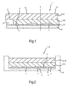
- Fig.1 shows a sectional view in side view of a section of a light strip according to the invention.
- Fig.2 shows the light strip 1 as a sectional view in front view.
- Fig.1 and Fig.2 has the present in the form of a light strip 1 lighting device on a band-shaped, flexible circuit board 2, the top or front 3 is equipped with arranged in series light emitting diodes 4.
- a back 5 of the circuit board 2 is on a bottom of an elongated, in cross-section U-shaped profile 6 (see Fig.2 ) attached.
- the profile 6 may include silicone as its base material in order to at least partially maintain a flexibility of the light strip 1.
- the profile 6 may in particular consist of an opaque material.
- the LEDs 4 radiate upward from the open side of the profile 6 addition, wherein the profile 6, the printed circuit board 2, 4 projects beyond.
- the electrical contacts 7 may, for example, be located on both sides of a separation point T, at which the light strip 1 or the molded printed circuit board 2, 4, 8 in two light strip sections 1a, 1b separable and thus can be assembled.
- the assembled circuit board 2, 4 is encapsulated with a potting layer 8 within the profile 6, which consists of two superposed potting layers 9, 10.
- the upper side 11 is not covered by the first potting layer 9 and has the light exit region of the light-emitting diode 4.
- the profile 6 and the first potting layer 9 protect the printed circuit board 2,4 up to the height of the upper side (s) 11 of the light emitting diode (s) 4, e.g. to fulfill an IP class.
- the first potting layer 9 is opaque and designed for a uniform color appearance in the same color as the profile 6. This may e.g. be achieved by a color additive (colored filler particles, etc.) to an otherwise non-colored base material.
- the assembled printed circuit board 2.4 remains up to the respective top side 11 of the light-emitting diode (s) 4 a view from the outside deprived.
- the first potting layer 9 may include silicone as the base material to provide good processability with high protection, good aging resistance and flexibility. Also occurs against the material of the profile 6 no mismatch, and it is achieved a very good connection with it.
- a second, now transparent or highly translucent potting compound 10 applied with a high transmissivity, for example made of silicone without added color.
- the second potting layer 10 advantageously has the same base material as the first potting layer 9.
- Figure 3 shows the light strip 1, in which the potting layer 8 has been removed on both sides of the separation point T on the adjacent contacts 7 of the light strip sections 1a, 1b also so that the contacts 7 are still covered by a thinner, remaining potting layer 12.
- the potting layer 8 can be removed, for example, by first providing the light strip 1 on both sides of the contacts 7 with respective vertical sections S1 and S2, as indicated by the arrows pointing downwards. These vertical sections S1 and S2 separate the potting layer 8 and the profile 6 to a maximum of the printed circuit board 2. Within the area bounded by the two vertical sections S1 and S2 are the contacts 7 adjacent to the separation point T. The vertical or vertical sections S1 and S2 are preferably set symmetrically to the separation point.
- the light band 1 (ie, its potting layer 8 and profile 6) is severed at least in the area bounded by the two vertical sections S1 and S2 by a horizontal section S3 at a height which is higher than a height of the electrical contacts. 7 This leaves the thinner residual potting layer 12 on the contacts 7.
- the potting layer 8 and the profile 6 can be temporarily frozen or embrittled before introduction of the sections S1 to S3, eg by applying a cold spray, liquid nitrogen, etc.
- Figure 4 shows a side view of a possible tool for removing the potting layer 8 and the profile.
- the tool is designed as a cutting pliers Z, which has an effective range with a double cutting edge D with two parallel, vertically aligned individual cutting edges, which are provided to introduce the vertical cuts S1 and S2 in the light strip 1.
- the double cutting edge D opposite leg of the pliers head has a receptacle A for the light strip 1 on.
- the cutting pliers Z on a horizontally movable blade H, which is provided for introducing the horizontal section S3.
- the horizontally movable cutting edge H can be articulated via a push rod G to the handles F of the cutting tong Z.
- the double cutting D moves to the light strip 1, cuts into this and thus generates the vertical cuts S1 and S2.
- the horizontally movable blade H is pushed forward, cuts laterally and horizontally into the light strip 1 and thus generates the horizontal section S3. In this case, a tilting of the light strip 1 is prevented by the double cutting edge D.
- the light strip 1 may have one or more corresponding markings (o.Fig.).
- the cut-out material can be removed, and the interfaces formed by the cuts S1 to S3 can be cleaned and / or deburred.
- Figure 5 shows a section of the light strip section 1a in a region of its longitudinal end 13, which passes through a severing or severing of the luminous band 1 has been formed along the separation point T following the removal of the potting layer 8 and the profile 6.
- an open copper cutting edge is present, which is formed due to severed conductor tracks.
- FIG 6 shows the section of the light strip section 1a Figure 5 , wherein now a connection element in the form of a connector 15 according to a first embodiment has been applied to the remaining potting layer 12.
- the connector 15 is constructed or assembled in two parts from an upper connector part 15a and a lower connector part 15b.
- the lower connector part 15b is thus applied from below in the region of the end 13 to a rear side 16 of the light strip section 1a, so that the lower connector part 15b covers there as well as the back 16 and a lower part of the cut edge 14.
- the lower connector part 15b and the connector 15 can not be deducted from the end 13, the lower connector part 15b is provided at its contact surface 17 with the back 16 with a structuring, here: a corrugation or cutting lips 18, which in the Rear 16, which is formed by the profile 6 made of silicone, can press.
- a sealing of the connector 15 on the light strip section 1a can be achieved, which can further improve a protection classification.
- the cutting lips 18 cut or press into the material of the profile 6 and form a seal by a warping of the potting material (for example silicone).
- the upper connector part 15a is placed over the entire surface of the rest of the casting layer 12, wherein the upper Connector part 15 a, the cutting edge 14 surrounds to cover the upper part, which is not covered by the lower connector part 15 b, cover.
- the upper connector part 15a contacts the not-removed casting layer 8 and also has a notch or cutting lip 18 at this contact surface in order to also loosen the upper connector part 15a or the connector 15 of FIG to prevent the light strip section 1a.
- the upper connector part 15a and the lower connector part 15b are compressed and latched, e.g. by means of locking hooks.
- the connector 15 is formed here in the form of a female socket and has for receiving a connector pin 20 a frontally open connector receptacle 19.
- a connection pin or contact pin 21 which can project through an opening 22, for example a slot in the connector receptacle 19 and a housing 23 of the upper connector part 15 a down or in the direction of the remaining potting 12.
- the contact pin 21 may already protrude through the opening 22 before a first use (insertion of the connector pin 20) or not yet protrude through the opening 22. With insertion of the connector pin 20 (as indicated by the arrow) this hits an upper side 24 of the contact pin 21 and pushes it down through the opening 22 and on through the remaining potting layer 12 except for the associated contact 7.
- the contact pin 21 so pierces it the remaining potting layer 12.
- the plug pin 20 can thus contact the contact 7 via the contact pin 21.
- Figure 6 shows the contact pin 21, as he contacted the contact 7, not plugged in for the sake of clarity with the pin 20.
- the contact pin 21 can easily pierce the remaining potting layer 12 and penetrate into the contact 7 have on its lower side a cutting edge and thus be formed as a cutting contact.
- the contact pin 21 is resiliently supported or elastically deformable to prevent breakage or damage due to plastic deformation.
- the remaining potting layer 12 serves as a sealing material for the connector 15, in particular as a seal for the contact pin 21st
- FIG. 7 shows the section of the light strip section 1a Figure 5 , wherein now on the remaining potting layer 12, a female connector 25 has been applied according to a second embodiment.
- An upper connector part 25a of the connector 25 now has a connector receptacle 26, in which no contact pin is arranged. Rather, the contact pin 27 connects to a rear side of the connector receptacle 26 and protrudes downwards beyond a housing 28 of the upper connector part 25a.
- the contact pin 27 is housed in a downwardly open housing space 29, in which he can move.
- the housing 28 is now not at its rear contact edge 30 with a cutting lip o. upgraded, but has for sealing a sealing element 31 which is inserted in a corresponding groove 32.
- a lower connector part 25b of the connector 25 is similar to the lower connector part 15b, except that also here instead of a cutting lip, a sealing element 31 is used for sealing.
- the upper connector part 25a and the lower connector part 25b attached to the first light strip portion 1a and then be pressed together, for example, locked and / or glued.
- the contact pin 27 has a lower cutting edge, so that he at the assembly cuts into the remaining potting layer 12 and contacts the contact 7.
- the connector 25 may also be listed in one piece and e.g. be pushed onto the first light strip section 1a.
- the matching male connector 33 mounted on the second light-band portion 1b is constructed similarly to the connector 25, except that instead of the connector receptacle 26, a connector pin 34 will be provided. Both connectors 25 and 33 have frontally a circumferential annular groove 35 for receiving an O-ring 36.
- Figure 8 shows a first light strip portion 1a with a female connector 37 mounted thereon according to a third embodiment.
- the female connector 37 (and, for example, the male counterpart, o.Abb.) Differs from the connector 25 only in that instead of a separate sealing element 31 a fixed to the housing 28 sealing lip 38 is used.
- the profile in the region of the longitudinal end of a light strip or light strip section, the profile can be completely removed so that the plug-in connectors contact the printed circuit board from below.
Landscapes
- Engineering & Computer Science (AREA)
- General Engineering & Computer Science (AREA)
- Metallurgy (AREA)
- Manufacturing & Machinery (AREA)
- Microelectronics & Electronic Packaging (AREA)
- Fastening Of Light Sources Or Lamp Holders (AREA)
- Led Device Packages (AREA)
Description
- Die Erfindung betrifft ein Verfahren zum Kontaktieren einer Leuchtvorrichtung, wobei die Leuchtvorrichtung eine Leiterplatte aufweist, welche zumindest teilweise von einer Vergussschicht bedeckt ist; wobei die Leuchtvorrichtung an einer Trennstelle in zwei Leuchtvorrichtungsabschnitte auftrennbar ist und jeder der Leuchtvorrichtungsabschnitte benachbart zu der Trennstelle jeweils mindestens einen elektrischen Kontakt aufweist. Die Erfindung betrifft auch ein Werkzeug zum Durchführen des Verfahrens.
- Es sind in mehrere Abschnitte trennbare flexible LED-Bänder bekannt, z.B. der LINEARLight-Serie der Fa. Osram, welche in einem bandförmigen U-Profil aus Silikon eingelegt sind und in dem Profil mit einer Vergussmasse aus Silikon vergossen sind. Hierbei werden zur Kontaktierung der aufgetrennten LED-Bandabschnitte deren stirnseitige Kontakte freigelegt und kontaktiert. Bei der Kontaktierung mit einem Kontaktierungselement kann eine Abdichtung des LED-Bands oder LED-Bandabschnitts so weit entfernt sein, dass eine Schutzfunktion oder Schutzklasse beeinträchtigt wird. Um die Schutzfunktion oder Schutzklasse aufrecht zu erhalten, ist es bekannt, das Kontaktierungselement nachträglich mit Silikon zu vergießen, was aufwändig ist.
-
EP0911573 offenbart ein in mehrere Abschnitte trennbares flexibles LED-Band. Die Abschnitte können an geeigneten Trennstellen abgetrennt werden. An den Trennstellen können Kontaktstifte in eine Stirnseite des abgetrenriten Abschnittes eirigesteckt werden.DE20315756U offenbart eine Abisolierzange für Flachkabel. - Alternativ sind vergossene LED-Bänder mit mitvergossenen Steckverbindern bekannt. Dabei tritt der Nachteil auf, dass dies eine Flexibilität bei einer Längenkonfektionierung herabsetzt und vergleichsweise teuer ist.
- Es ist die Aufgabe der vorliegenden Erfindung, die Nachteile des Standes der Technik zumindest teilweise zu beseitigen und insbesondere eine Möglichkeit für eine einfache Kontaktierung vergossener Leuchtbänder bereitzustellen, welche eine Schutzfunktion aufrechterhalten kann.
- Diese Aufgabe wird gemäß den Merkmalen der unabhängigen Ansprüche gelöst. Bevorzugte Ausführungsformen sind insbesondere den abhängigen Ansprüchen entnehmbar.
- Die Aufgabe wird gelöst durch ein Verfahren zum Kontaktieren einer Leuchtvorrichtung, wobei die Leuchtvorrichtung eine Leiterplatte aufweist, welche zumindest teilweise von einer Vergussschicht bedeckt ist; wobei die Leuchtvorrichtung an einer Trennstelle in zwei Leuchtvorrichtungsabschnitte auftrennbar ist und jeder der Leuchtvorrichtungsabschnitte benachbart zu der Trennstelle jeweils mindestens einen elektrischen Kontakt aufweist; wobei das Verfahren mindestens die folgenden Schritte aufweist:
- Entfernen zumindest der Vergussschicht beidseitig der Trennstelle über die benachbarten Kontakte der Leuchtvorrichtungsabschnitte hinaus so, dass die Kontakte von einer dünneren, restlichen Vergussschicht bedeckt bleiben;
- Auftrennen der Leuchtvorrichtung an der Trennstelle;
- Befestigen eines Anschlusselements zumindest auf der restlichen Vergussschicht zumindest eines der Leuchtvorrichtungsabschnitte,
- wobei das Anschlusselement mindestens ein Kontaktierungselement aufweist, welches einen jeweiligen mit der restlichen Vergussschicht bedeckten Kontakt nach einem Durchtrennen oder Durchstoßen der restlichen Vergussschicht kontaktiert.
- Durch dieses Verfahren sind die Kontakte aufgrund der dünne(re)n restlichen Vergussschicht leicht erreichbar und mittels des Durchstoßens ohne weiteren Aufwand kontaktierbar. Die restliche Vergussschicht wirkt zudem gegenüber dem Kontaktierungselement als eine Abdichtung, so dass auf einen zusätzlichen Abdichtungsschritt (z.B. durch ein Vergießen) verzichtet werden kann.
- Das Anschlusselement dient dem elektrischen Anschluss der Leiterplatte zur Energieübertragung und/oder Datenübertragung.
- Unter einem elektrischen Kontakt der Leiterplatte kann jegliche für eine externe Kontaktierung geeignete Stelle der Verdrahtung verwendet werden, z.B. eine ausreichend breite Leiterbahn oder ein speziell zur Kontaktierung vorgesehener Kontaktbereich wie ein Kontakthöcker oder ein Kontaktfeld ("Kontaktpad") usw.
- Es ist eine Ausgestaltung, dass zumindest die Vergussschicht mittels zweier im Wesentlichen senkrechter Schnitte in dem Bereich beidseitig der Trennstelle über die Kontakte hinaus eingeschnitten wird (insbesondere bis zu der Leiterplatte) und zumindest zwischen den vertikalen Schnitten zusätzlich mittels mindestens eines horizontalen Schnitts auf einer Höhe oberhalb der Kontakte seitlich durchtrennt wird. So kann die Leuchtvorrichtung mit einfachen Mitteln präpariert werden.
- Es ist noch eine Ausgestaltung, dass die Leiterplatte und die Vergussschicht in einem Profil aufgenommen sind und zumindest ein Teil des Profils beidseitig der Trennstelle zusammen mit der Vergussschicht entfernt wird, vorzugsweise im Rahmen der gleichen Trennschritte. Das Profil kann dabei ebenfalls nur oberhalb der Kontakte entfernt werden, was besonders einfach und schnell durchführbar ist. Alternativ kann das Profil beispielsweise in dem durch die senkrechten Schnitte begrenzten Bereich vollständig entfernt werden, um eine kompakte Form des Anschlusselements zu ermöglichen. Auch kann das Anschlusselement so unterseitig direkt an die Leiterplatte aufgesetzt werden.
- Es ist zudem eine Ausgestaltung, dass das Anschlusselement zumindest auf einen Teil der restlichen Vergussschicht aufgesetzt wird und für eine elektrische Verbindung zu dem Kontakt die über dem Kontakt befindliche restliche Vergussschicht mittels eines elektrischen Kontaktierungselements durchstößt. Insbesondere kann das Anschlusselement auf die gesamte restliche Vergussschicht und optional zusätzlich auf die nicht heruntergedünnte Vergussschicht aufgesetzt werden, um einen Grad an Dichtigkeit weiter zu erhöhen.
- Es ist ferner eines Ausgestaltung, dass das Kontaktierungselement eine Schneidkante zum schneidenden oder durchstoßenden Trennen der restlichen Vergussschicht aufweist. Dadurch wird eine Kontaktierung erleichtert.
- Das Anschlusselement kann insbesondere ein Steckverbinder sein.
- Es ist noch eine Ausgestaltung, dass das Kontaktierungselement sich teilweise in einer Steckeraufnahme befindet und zumindest bei einem ersten Einstecken eines Steckstifts in die Steckeraufnahme das Kontaktierungselement mittels des Steckstifts durch die restliche Vergussschicht hindurch auf den Kontakt gedrückt wird. Dadurch kann ein hoher Kontaktdruck und folglich eine sichere Kontaktierung erreicht werden.
- Es ist noch eine weitere Ausgestaltung, dass das Kontaktierungselement bei einer Aufsatzbewegung des Anschlusselements durch die restliche Vergussschicht hindurch auf den Kontakt gedrückt wird.
- Es ist eine Weiterbildung, dass die Aufsatzbewegung des Anschlusselements eine Gleitbewegung umfasst. Dadurch kann der mindestens eine elektrische Kontakt beispielsweise bei einem Aufschieben des Anschlusselements auf die Leuchtvorrichtung kontaktiert werden.
- Es ist noch eine Weiterbildung, dass die Aufsatzbewegung des Anschlusselements eine senkrechte Aufsatzbewegung umfasst. Dadurch kann der mindestens eine elektrische Kontakt beispielsweise bei einem Aufdrücken des Anschlusselements auf die Leuchtvorrichtung kontaktiert werden. So kann hierbei beispielsweise das Verbindungselement zweiteilig ausgeführt sein, wobei die beiden Teile an der Leuchtvorrichtung angesetzt und danach unter einem Druck verrastet werden. Der Rastvorgang stellt dabei die senkrechte Aufsatzbewegung bereit. Alternativ oder zusätzlich kann der elektrische Kontakt durch Clipsen, Klemmen, Verschrauben usw. kontaktiert und/oder befestigt werden.
- Es ist noch eine weitere Ausgestaltung, dass die Leiterplatte eine bandförmige Leiterplatte, insbesondere bandförmige flexible Leiterplatte, ist. Diese lässt sich besonders einfach mittels des genannten Verfahrens kontaktieren, insbesondere in einem Bereich längsseitiger Enden.
- Es ist noch eine weitere Ausgestaltung, dass das Vergussmaterial ein elastisches Grundmaterial ausweist, insbesondere Silikon. Dadurch kann eine mechanische Flexibilität der Leuchtvorrichtung, insbesondere Leuchtbands, zumindest eingeschränkt aufrechterhalten werden.
- Die Aufgabe wird auch gelöst durch ein Werkzeug zum Durchführen des Verfahrens, wobei das Werkzeug eine Schneidzange mit einer senkrecht stehenden Doppelschneide und einer horizontal beweglichen Schneide ist. So kann der Schritt des Entfernens zumindest der Vergussschicht einfach und innerhalb eines einzigen Ablaufschritts durchgeführt werden.
- Die Aufgabe wird ferner gelöst durch ein Anschlusselement zum Aufsatz auf eine Leuchtvorrichtung, wobei der Steckverbinder mindestens ein Kontaktierungselement zum Durchtrennen oder Durchstoßen einer restlichen Vergussschicht aufweist.
- Es ist eine Weiterbildung, dass das Kontaktierungselement eine Schneidkante aufweist. Dies erleichtert eine Durchtrennung oder Durchstoßung der restlichen Vergussschicht.
- Die Leuchtvorrichtung kann dazu insbesondere eine mit einer Vergussschicht bedeckte Leiterplatte aufweisen, wobei die Leuchtvorrichtung mindestens einen Bereich mit einer dünneren restlichen Vergussschicht aufweist, wobei mindestens ein elektrischer Kontakt von der restlichen Vergussschicht bedeckt ist.
- Durch die Erfindung wird insbesondere erreicht, dass:
- eine Trennung von vergossenen Leiterplatten, insbesondere flexiblen Leuchtbändern, kundenseitig möglich ist, evtl. mit Spezialwerkzeug;
- eine einfache, dichte Montage eines Anschlusselements, insbesondere Steckverbinders, durch einen Kunden ohne Verlust der IP-Klassifizierung möglich ist,
- eine kundenseitige Längenkonfektionierung leicht erfolgen kann
- kein nennenswerter Verlust der Biegbarkeit flexibler Leiterplatten auftritt,
- das die Anschlusselemente mit anderen Systemen kombinierbar sind,
- die Fertigung (insbesondere ein Vergussschritt) vereinfacht wird, da nicht in diskreten Längen gefertigt werden muss, sondern quasi endlos gefertigt werden kann.
- In den folgenden Figuren wird die Erfindung anhand von Ausführungsbeispielen schematisch genauer beschrieben. Dabei können zur Übersichtlichkeit gleiche oder gleichwirkende Elemente mit gleichen Bezugszeichen versehen sein.
- Fig.1
- zeigt als Schnittdarstellung in Seitenansicht einen Ausschnitt aus einem trennbaren Leuchtband;
- Fig.2
- zeigt das trennbare Leuchtband als Schnittdarstellung in Vorderansicht;
- Fig.3
- zeigt als Schnittdarstellung in Seitenansicht das Leuchtband mit einer beidseitig einer Trennstelle entfernten Vergussschicht;
- Fig.4
- zeigt in Seitenansicht ein mögliches Werkzeug zum Entfernen der Vergussschicht;
- Fig.5
- zeigt als Schnittdarstellung in Seitenansicht einen Leuchtbandabschitt im Bereich eines abgetrennten Endes;
- Fig.6
- zeigt einen Leuchtbandabschnitt mit einem daran endseitig montierten Steckverbinder gemäß einer ersten Ausführungsform;
- Fig.7
- zeigt einen Leuchtbandabschnitt mit einem daran endseitig montierten Steckverbinder gemäß einer zweiten Ausführungsform; und
- Fig.8
- zeigt einen Leuchtbandabschnitt mit einem daran endseitig montierten Steckverbinder gemäß einer dritten Ausführungsform.
-
Fig.1 zeigt als Schnittdarstellung in Seitenansicht einen Ausschnitt aus einem erfindungsgemäßen Leuchtband 1.Fig.2 zeigt das Leuchtband 1 als Schnittdarstellung in Vorderansicht. - Bezug nehmend auf
Fig.1 und Fig.2 weist die in Form eines Leuchtbands 1 vorliegende Leuchtvorrichtung eine bandförmige, flexible Leiterplatte 2 auf, deren Oberseite oder Vorderseite 3 mit in Reihe angeordneten Leuchtdioden 4 bestückt ist. Eine Rückseite 5 der Leiterplatte 2 ist auf einem Boden eines länglichen, im Querschnitt U-förmigen Profils 6 (sieheFig.2 ) befestigt. Das Profil 6 kann Silikon als sein Grundmaterial aufweisen, um eine Biegsamkeit des Leuchtbands 1 zumindest teilweise beibehalten zu können. Das Profil 6 kann insbesondere aus einem blickdichten Material bestehen. Die Leuchtdioden 4 strahlen nach oben aus der offenen Seite des Profils 6 hinaus, wobei das Profil 6 die bestückte Leiterplatte 2, 4 nach oben überragt. - An der Vorderseite 3 der Leiterplatte 2 befindet sich eine Verdrahtung für daran befestigte Elemente (Leuchtdioden 4 und ggf. weitere elektronische Bauelemente wie Treiberbausteine, Kondensatoren und/oder Widerstände), wobei von der Verdrahtung nur elektrische Kontakte 7 gezeigt sind. Die elektrischen Kontakte 7 können sich beispielsweise beidseitig einer Trennstelle T befinden, an welcher das Leuchtband 1 bzw. die vergossene Leiterplatte 2, 4, 8 in zwei Leuchtbandabschnitte 1a, 1b trennbar und somit konfektionierbar ist.
- Die bestückte Leiterplatte 2, 4 ist mit einer Vergussschicht 8 innerhalb des Profils 6 vergossen, welche aus zwei übereinanderliegenden Vergusslagen 9, 10 besteht. Eine untere erste Vergusslage 9, welche zuerst aufgebracht worden ist, bedeckt die Leiterplatte 2 bis zu einer Oberseite 11 der Leuchtdioden 4. Die Oberseite 11 ist nicht durch die erste Vergusslage 9 bedeckt und weist den Lichtaustrittsbereich der Leuchtdiode 4 auf. Das Profil 6 und die erste Vergusslage 9 schützen die bestückte Leiterplatte 2,4 bis auf die Höhe der Oberseite(n) 11 der Leuchtdiode(n) 4, z.B. zur Erfüllung einer IP-Klasse.
- Die erste Vergusslage 9 ist lichtundurchlässig und für eine farblich einheitliche Anmutung in der gleichen Farbe ausgebildet wie das Profil 6. Dies kann z.B. durch einen Farbzusatz (farbige Füllpartikel usw.) zu einem ansonsten nichtfarbigen Grundmaterial erreicht werden. So bleibt die bestückte Leiterplatte 2,4 bis auf die jeweilige Oberseite 11 der Leuchtdiode(n) 4 einem Blick von Außen entzogen. Die erste Vergusslage 9 kann Silikon als Grundmaterial aufweisen, um eine gute Verarbeitbarkeit mit hohem Schutz, guter Alterungsbeständigkeit und einer Biegsamkeit bereitzustellen. Auch tritt gegenüber dem Material des Profils 6 keine Fehlanpassung auf, und es wird eine sehr gute Verbindung damit erreicht.
- Zum Schutz auch der Oberseite 11 der Leuchtdiode(n) 4 ist auf der ersten Vergusslage 9 eine zweite, nun transparente oder hochgradig lichtdurchlässige Vergusslage 10 mit einer hohen Transmissivität aufgebracht, z.B. aus Silikon ohne Farbzusatz. Durch die zweite Vergusslage 10 wird die bestückte Leiterplatte 2, 4 vollständig vergossen und somit geschützt. Die zweite Vergusslage 10 weist vorteilhafterweise das gleiche Grundmaterial auf wie die erste Vergusslage 9.
-
Fig.3 zeigt das Leuchtband 1, bei dem die Vergussschicht 8 beidseitig der Trennstelle T über die benachbarten Kontakte 7 der Leuchtbandabschnitte 1a, 1b hinaus so entfernt worden ist, dass die Kontakte 7 immer noch von einer dünneren, restlichen Vergussschicht 12 bedeckt sind. - Die Vergussschicht 8 kann beispielsweise entfernt werden, indem zunächst das Leuchtband 1 beidseitig der Kontakte 7 mit jeweiligen senkrechten Schnitten S1 und S2 versehen wird, wie durch die nach unten zeigenden Pfeile angedeutet. Diese senkrechten Schnitte S1 und S2 trennen die Vergussschicht 8 und das Profil 6 maximal bis zu der Leiterplatte 2 auf. Innerhalb des durch die beiden senkrechten Schnitte S1 und S2 begrenzten Bereichs befinden sich die der Trennstelle T benachbarten Kontakte 7. Die senkrechten bzw. vertikalen Schnitte S1 und S2 werden vorzugsweise symmetrisch zu der Trennstelle gesetzt.
- Gleichzeitig oder folgend wird das Leuchtband 1 (d.h., dessen Vergussschicht 8 und Profil 6) zumindest in dem durch die beiden senkrechten Schnitte S1 und S2 begrenzten Bereich durch einen horizontalen Schnitt S3 auf einer Höhe durchtrennt, welche höher ist als eine Höhe der elektrischen Kontakte 7. Dadurch verbleibt die dünnere restliche Vergussschicht 12 auf den Kontakten 7.
- Zur mechanisch einfachen und präzisen Trennung können die Vergussschicht 8 und das Profil 6 vor einem Einbringen der Schnitte S1 bis S3 zeitweilig erstarrt oder versprödet werden, z.B. durch ein Aufbringen eines Kältesprühmittels, flüssigen Stickstoffs usw.
-
Fig.4 zeigt in Seitenansicht ein mögliches Werkzeug zum Entfernen der Vergussschicht 8 und des Profils. Das Werkzeug ist als eine Schneidzange Z ausgebildet, welche einen Wirkbereich mit einer Doppelschneide D mit zwei parallelen, senkrecht ausgerichteten Einzelschneiden aufweist, welche dazu vorgesehen sind, die senkrechten Schnitte S1 und S2 in das Leuchtband 1 einzubringen. Für eine entsprechende Positionierung des Leuchtbands 1 weist der der Doppelschneide D entgegengesetzte Schenkel des Zangenkopfs eine Aufnahme A für das Leuchtband 1 auf. Zusätzlich weist die Schneidzange Z eine horizontal bewegliche Schneide H auf, welche zur Einbringung des horizontalen Schnitts S3 vorgesehen ist. Die horizontal bewegliche Schneide H kann über ein Schubgestänge G an den Griffen F der Schneidzange Z angelenkt sein. - Bei einer Betätigung der Schneidzange Z durch ein Zusammendrücken der Griffe F bewegt sich die Doppelschneide D auf das Leuchtband 1 zu, schneidet in dieses ein und erzeugt so die senkrechten Schnitte S1 und S2. Gleichzeitig wird die horizontal bewegliche Schneide H nach vorne geschoben, schneidet seitlich und horizontal in das Leuchtband 1 ein und erzeugt so den horizontalen Schnitt S3. Dabei wird eine Verkippung des Leuchtbands 1 durch die Doppelschneide D verhindert.
- Zur korrekten Positionierung der Schneidzange Z bezüglich der Trennstelle T des Leuchtbands 1 kann das Leuchtband 1 eine oder mehrere entsprechende Markierungen (o.Abb.) aufweisen.
- Im Folgenden kann das ausgeschnittene Material entfernt werden, und es können die durch die Schnitte S1 bis S3 entstandenen Schnittstellen gesäubert und/oder entgratet werden.
-
Fig.5 zeigt einen Ausschnitt aus dem Leuchtbandabschnitt 1a in einem Bereich seines längsseitigen Endes 13, welches durch ein Auftrennen oder Durchtrennen des Leuchtbands 1 entlang der Trennstelle T folgend auf das Entfernen der Vergussschicht 8 und des Profils 6 gebildet worden ist. An dem Ende 13 bzw. in einer geringen Entfernung von einer zugehörigen Schnittkante 14 befinden sich die Kontakte 7, die von der restlichen Vergussschicht 12 bedeckt sind. An der Schnittkante 14 ist eine offene Kupferschnittkante vorhanden, welche aufgrund durchtrennter Leiterbahnen gebildet wird. -
Fig.6 zeigt den Ausschnitt aus dem Leuchtbandabschnitt 1a ausFig.5 , wobei nun auf der restlichen Vergussschicht 12 ein Anschlusselement in Form eines Steckverbinders 15 gemäß einer ersten Ausführungsform aufgebracht worden ist. Der Steckverbinder 15 ist zweiteilig aus einem oberen Steckverbinderteil 15a und einem unteren Steckverbinderteil 15b aufgebaut oder zusammengesetzt. - Das untere Steckverbinderteil 15b wird so von unten im Bereich des Endes 13 an eine Rückseite 16 des Leuchtbandabschnitts 1a angelegt, so dass das untere Steckverbinderteil 15b dort außer der Rückseite 16 auch einen unteren Teil der Schnittkante 14 abdeckt. Damit das untere Steckverbinderteil 15b und der Steckverbinder 15 nicht von dem Ende 13 abgezogen werden können, ist das untere Steckverbinderteil 15b an seiner Kontaktfläche 17 mit der Rückseite 16 mit einer Strukturierung, hier: einer Riffelung bzw. Schneidlippen 18, versehen, welche sich in die Rückseite 16, die durch das Profil 6 aus dem Silikon gebildet wird, eindrücken können. Durch diese Schneidlippen 18 kann eine Abdichtung des Steckverbinders 15 an dem Leuchtbandabschnitt 1a erreicht werden, was eine Schutzklassifikation weiter verbessern kann. Dazu schneiden bzw. drücken die Schneidlippen 18 in das Material des Profils 6 ein und bilden eine Dichtung durch eine Verwölbung des Vergussmaterials (z.B. Silikon).
- Von oben wird das obere Steckverbinderteil 15a vollflächig auf die restliche Vergussschicht 12 aufgesetzt, wobei das obere Steckverbinderteil 15a die Schnittkante 14 umgreift, um deren oberen Teil, welcher nicht durch das untere Steckverbinderteil 15b abgedeckt ist, abzudecken. An einem von dem Ende 13 bzw. der Schnittkante 14 wegzeigenden Rand kontaktiert das obere Steckverbinderteil 15a die nicht entfernte Vergussschicht 8 und weist an dieser Kontaktfläche ebenfalls eine Kerbe oder Schneidlippe 18 auf, um ein Lösen auch des oberen Steckverbinderteils 15a bzw. des Steckverbinders 15 von dem Leuchtbandabschnitt 1a zu verhindern.
- Zur Montage des Steckverbinders 15 werden das obere Steckverbinderteil 15a und das untere Steckverbinderteil 15b zusammengedrückt und dabei verrastet, z.B. mittels Rasthaken.
- Der Steckverbinder 15 ist hier in Form einer weiblichen Buchse ausgebildet und weist zur Aufnahme eines Steckerstifts 20 eine stirnseitig offene Steckeraufnahme 19 auf. In der Steckeraufnahme 19 befindet sich ein Anschlussstift oder Kontaktstift 21, welcher durch eine Öffnung 22, z.B. einen Schlitz, in der Steckeraufnahme 19 und einem Gehäuse 23 des oberen Steckverbinderteils 15a nach unten bzw. in Richtung der restlichen Vergussschicht 12 ragen kann. Der Kontaktstift 21 kann vor einem ersten Gebrauch (Einführen des Steckerstifts 20) bereits ansatzweise durch die Öffnung 22 ragen oder noch nicht durch die Öffnung 22 ragen. Mit Einführen des Steckerstifts 20 (wie durch den Pfeil angedeutet) trifft dieser auf eine Oberseite 24 des Kontaktstifts 21 und drückt diesen nach unten durch die Öffnung 22 und weiter durch die restliche Vergussschicht 12 bis auf den zugehörigen Kontakt 7. Der Kontaktstift 21 durchstößt also dabei die restliche Vergussschicht 12. Der Steckerstift 20 kann somit den Kontakt 7 über den Kontaktstift 21 kontaktieren.
Fig.6 zeigt den Kontaktstift 21, wie er den Kontakt 7 kontaktiert, nur zur besseren Übersichtlichkeit mit dem Steckerstift 20 nicht eingesteckt. Der Kontaktstift 21 kann zum einfachen Durchstoßen der restlichen Vergussschicht 12 und Eindringen in den Kontakt 7 an seiner unteren Seite eine Schneidkante aufweisen und also als ein Schneidkontakt ausgebildet sein. - Der Kontaktstift 21 ist federnd gelagert oder elastisch verformbar, um ein Brechen oder eine Beschädigung durch eine plastische Verformung zu vermeiden.
- Die restliche Vergussschicht 12 dient als Dichtmaterial für den Steckverbinder 15, insbesondere als eine Dichtung für den Kontaktstift 21.
-
Fig.7 zeigt den Ausschnitt aus dem Leuchtbandabschnitt 1a ausFig.5 , wobei nun auf der restlichen Vergussschicht 12 ein weiblicher Steckverbinder 25 gemäß einer zweiten Ausführungsform aufgebracht worden ist. Ein oberes Steckverbinderteil 25a des Steckverbinders 25 weist nun eine Steckeraufnahme 26 auf, in welcher kein Kontaktstift angeordnet ist. Vielmehr schließt sich der Kontaktstift 27 an einer Rückseite der Steckeraufnahme 26 an und ragt nach unten über ein Gehäuse 28 des oberen Steckverbinderteils 25a hinaus. Dazu ist der Kontaktstift 27 in einem nach unten offenen Gehäuseraum 29 untergebracht, in dem er sich bewegen kann. Das Gehäuse 28 ist an seinem rückwärtigen Kontaktrand 30 nun nicht mit einer Schneidlippe o.ä. aufgerüstet, sondern weist für eine Abdichtung ein Dichtelement 31 auf, das in einer entsprechenden Nut 32 eingesetzt ist. Ein unteres Steckverbinderteil 25b des Steckverbinders 25 gleicht dem unteren Steckverbinderteil 15b, außer dass auch hier statt einer Schneidlippe ein Dichtelement 31 zur Abdichtung verwendet wird. - Zur Montage des Steckverbinders 25 können wie bei der ersten Ausführungsform das obere Steckverbinderteil 25a und das untere Steckverbinderteil 25b an dem ersten Leuchtbandabschnitt 1a angesetzt und dann verbindend zusammengepresst werden, z.B. verrastet und/oder verklebt werden. Auch hier weist der Kontaktstift 27 eine untere Schneidkante auf, so dass er bei der Montage in die restliche Vergussschicht 12 einschneidet und den Kontakt 7 kontaktiert.
- Der Steckverbinder 25 kann auch einstückig aufgeführt sein und z.B. auf den ersten Leuchtbandabschnitt 1a aufgeschoben werden.
- Der passende, an dem zweiten Leuchtbandabschnitt 1b montierte männliche Steckverbinder 33 ist gleichartig zu dem Steckverbinder 25 aufgebaut, außer dass statt der Steckeraufnahme 26 ein Steckerstift 34 vorhanden sein wird. Beide Steckverbinder 25 und 33 weisen stirnseitig eine umlaufende Ringnut 35 zur Aufnahme eines O-Rings 36 auf.
-
Fig.8 zeigt einen ersten Leuchtbandabschnitt 1a mit einem daran endseitig montierten weiblichen Steckverbinder 37 gemäß einer dritten Ausführungsform. Der weibliche Steckverbinder 37 (und z.B. auch das männliche Gegenstück, o.Abb.) unterscheidet sich von dem Steckverbinder 25 lediglich dadurch, dass anstelle eines separaten Dichtelements 31 eine an dem Gehäuse 28 befestigte Dichtlippe 38 verwendet wird. - Selbstverständlich ist die vorliegende Erfindung nicht auf die gezeigten Ausführungsbeispiele beschränkt.
- So kann im Bereich des längsseitigen Endes eines Leuchtbands oder Leuchtbandabschnitts das Profil vollständig entfernt werden, so dass die Steckverbinder von unten die Leiterplatte kontaktieren.
-
- 1
- Leuchtband
- 1a
- Leuchtbandabschnitt
- 1b
- Leuchtbandabschnitt
- 2
- Leiterplatte
- 3
- Vorderseite
- 4
- Leuchtdiode
- 5
- Rückseite
- 6
- Profil
- 7
- elektrischer Kontakt
- 8
- Vergussschicht
- 9
- erste Vergusslage
- 10
- zweite Vergusslage
- 11
- Oberseite der Leuchtdiode
- 12
- restliche Vergussschicht
- 13
- längsseitiges Ende
- 14
- Schnittkante
- 15
- Steckverbinder
- 15a
- oberes Steckverbinderteil
- 15b
- unteres Steckverbinderteil
- 16
- Rückseite
- 17
- Kontaktfläche
- 18
- Schneidlippe
- 19
- Steckeraufnahme
- 20
- Steckerstift
- 21
- Kontaktstift
- 22
- Öffnung
- 23
- Gehäuse des oberen Steckverbinderteils
- 24
- Oberseite des Kontaktstifts
- 25
- Steckverbinder
- 25a
- oberes Steckverbinderteil
- 25b
- unteres Steckverbinderteil
- 26
- Steckeraufnahme
- 27
- Kontaktstift
- 28
- Gehäuse
- 29
- Gehäuseraum
- 30
- Kontaktrand
- 31
- Dichtelement
- 32
- Nut für das Dichtelement
- 33
- Steckverbinder
- 34
- Steckerstift
- 35
- Ringnut
- 36
- O-Ring
- 37
- Steckverbinder
- 38
- Dichtlippe
- A
- Aufnahme
- D
- Doppelschneide
- F
- Griff
- G
- Schubgestänge
- H
- horizontal bewegliche Schneide
- S1
- senkrechter Schnitt
- S2
- senkrechter Schnitt
- S3
- horizontaler Schnitt
- T
- Trennstelle
- Z
- Schneidzange
Claims (13)
- Verfahren zum Kontaktieren einer Leuchtvorrichtung (1, 1a, 1b), wobei- die Leuchtvorrichtung (1) eine Leiterplatte (2) aufweist, welche zumindest teilweise von einer Vergussschicht (8) bedeckt ist; wobei- die Leuchtvorrichtung (1) an einer Trennstelle (T) in zwei Leuchtvorrichtungsabschnitte (1a, 1b) auftrennbar ist und- jeder der Leuchtvorrichtungsabschnitte (1a, 1b) benachbart zu der Trennstelle (T) jeweils mindestens einen elektrischen Kontakt (7) aufweist;wobei das Verfahren mindestens die folgenden Schritte aufweist:- Entfernen zumindest der Vergussschicht (8) beidseitig der Trennstelle (T) über die benachbarten Kontakte (7) der Leuchtvorrichtungsabschnitte (1a, 1b) hinaus so, dass die Kontakte (7) von einer dünneren, restlichen Vergussschicht (12) bedeckt bleiben;- Auftrennen der Leuchtvorrichtung (1) an der Trennstelle (T);- Befestigen eines Anschlusselements (15; 25; 33; 37) zumindest auf der restlichen Vergussschicht (12) zumindest eines der Leuchtvorrichtungsabschnitte (1a, 1b),- wobei das Anschlusselement (15; 25; 33; 37) mindestens ein Kontaktierungselement (21; 27) aufweist, welches einen jeweiligen mit der restlichen Vergussschicht (12) bedeckten Kontakt (7) nach einem Durchtrennen oder Durchstoßen der restlichen Vergussschicht (12) kontaktiert.
- Verfahren nach Anspruch 1, wobei zumindest die Vergussschicht (8) mittels zweier im Wesentlichen senkrechter Schnitte (S1, S2) beidseitig der Trennstelle (T) über die Kontakte (7) hinaus eingeschnitten wird und zumindest zwischen den vertikalen Schnitten (S1, S2) zusätzlich mittels mindestens eines horizontalen Schnitts (S3) auf einer Höhe oberhalb der Kontakte (7) durchtrennt wird.
- Verfahren nach einem der vorhergehenden Ansprüche, wobei die Leiterplatte (2) und die Vergussschicht (8) in einem Profil (6) aufgenommen sind und zumindest ein Teil des Profils (6) beidseitig der Trennstelle (T) zusammen mit der Vergussschicht (8) entfernt wird.
- Verfahren nach einem der vorhergehenden Ansprüche, wobei das Anschlusselement zumindest auf einen Teil der restlichen Vergussschicht (12) aufgesetzt wird und für eine elektrische Verbindung zu dem Kontakt (7) die über dem Kontakt (7) befindliche restliche Vergussschicht (12) mittels eines Kontaktierungselements durchtrennt oder durchstößt.
- Verfahren nach Anspruch 4, wobei das Kontaktierungselement eine Schneidkante zum Durchtrennen oder Durchstoßen der restlichen Vergussschicht (12) aufweist.
- Verfahren nach einem der Ansprüche 4 bis 5, wobei das Anschlusselement ein Steckverbinder (15; 25; 33; 37) ist.
- Verfahren nach Anspruch 6, wobei das Kontaktierungselement sich teilweise in einer Steckeraufnahme (19; 26) befindet und zumindest bei einem ersten Einstecken eines Steckstifts (20; 34) in die Steckeraufnahme (19; 26) das Kontaktierungselement (21) mittels des Steckerstifts (20; 34) durch die restliche Vergussschicht (12) hindurch auf den Kontakt (7) gedrückt wird.
- Verfahren nach einem der vorhergehenden Ansprüche, wobei das Kontaktierungselement (27) bei einer Aufsatzbewegung des Anschlusselements (15; 25; 33; 37) durch die restliche Vergussschicht (12) hindurch auf den Kontakt (7) gedrückt wird.
- Verfahren nach Anspruch 8, wobei die Aufsatzbewegung des Anschlusselements (25; 33; 37) eine Gleitbewegung umfasst.
- Verfahren nach einem der Ansprüche 8 oder 9, wobei die Aufsatzbewegung des Anschlusselements (15) eine senkrechte Aufsatzbewegung umfasst.
- Verfahren nach einem der vorhergehenden Ansprüche, bei dem die Leiterplatte (2) eine bandförmige Leiterplatte (2), insbesondere bandförmige flexible Leiterplatte (2), ist.
- Verfahren nach einem der vorhergehenden Ansprüche, bei dem das Vergussmaterial (8) ein elastisches Grundmaterial ausweist, insbesondere Silikon.
- Werkzeug zum Durchführen eines Verfahrens nach einem der vorhergehenden Ansprüche, wobei das Werkzeug eine Schneidzange (Z) mit einer senkrecht stehenden Doppelschneide (D) und einer horizontal beweglichen Schneide (H) ist.
Applications Claiming Priority (2)
| Application Number | Priority Date | Filing Date | Title |
|---|---|---|---|
| DE102009054511A DE102009054511A1 (de) | 2009-12-10 | 2009-12-10 | Verfahren zum Kontaktieren einer Leuchtvorrichtung, Werkzeug zum Durchführen des Verfahrens und Anschlusselement zum Aufsatz auf eine Leuchtvorrichtung |
| PCT/EP2010/068315 WO2011069844A2 (de) | 2009-12-10 | 2010-11-26 | Verfahren zum kontaktieren einer leuchtvorrichtung, werkzeug zum durchführen des verfahrens und anschlusselement zum aufsatz auf eine leuchtvorrichtung |
Publications (2)
| Publication Number | Publication Date |
|---|---|
| EP2494265A2 EP2494265A2 (de) | 2012-09-05 |
| EP2494265B1 true EP2494265B1 (de) | 2014-07-02 |
Family
ID=43987407
Family Applications (1)
| Application Number | Title | Priority Date | Filing Date |
|---|---|---|---|
| EP10787725.0A Active EP2494265B1 (de) | 2009-12-10 | 2010-11-26 | Verfahren zum kontaktieren einer leuchtvorrichtung, werkzeug zum durchführen des verfahrens und anschlusselement zum aufsatz auf eine leuchtvorrichtung |
Country Status (5)
| Country | Link |
|---|---|
| US (1) | US8935846B2 (de) |
| EP (1) | EP2494265B1 (de) |
| CN (1) | CN102652241B (de) |
| DE (1) | DE102009054511A1 (de) |
| WO (1) | WO2011069844A2 (de) |
Cited By (1)
| Publication number | Priority date | Publication date | Assignee | Title |
|---|---|---|---|---|
| DE102017203870B4 (de) | 2017-03-09 | 2024-04-11 | Ifm Electronic Gmbh | Elektronisches Gerät der Automatisierungstechnik mit einer zweifach kunststoffumspritzten Elektronikplatine |
Families Citing this family (11)
| Publication number | Priority date | Publication date | Assignee | Title |
|---|---|---|---|---|
| EP2562470B1 (de) | 2011-08-24 | 2018-04-11 | OSRAM GmbH | Verfahren zur Herstellung einer Beleuchtungsvorrichtung und entsprechende Beleuchtungsvorrichtung |
| DE102011056570A1 (de) * | 2011-12-16 | 2013-06-20 | Osram Opto Semiconductors Gmbh | Lichtemittierende Bauelement-Anordnung |
| DE102012214264A1 (de) * | 2012-08-10 | 2014-02-13 | Robert Bosch Gmbh | Leiterplatte mit einem elektrischen Kontakt |
| US9022602B2 (en) * | 2012-08-28 | 2015-05-05 | Osram Sylvania Inc. | Modular multichannel connector system and method |
| DE102013201219A1 (de) | 2013-01-25 | 2014-07-31 | Osram Opto Semiconductors Gmbh | Leuchtmittel |
| US9151454B1 (en) * | 2013-09-09 | 2015-10-06 | Automated Assembly Corporation | Modular LED lighting apparatus |
| US9812831B2 (en) * | 2015-06-11 | 2017-11-07 | Osram Gmbh | Connector for lighting devices and corresponding method |
| WO2018013889A1 (en) * | 2016-07-15 | 2018-01-18 | Aculon, Inc | Coated articles that demonstrate push-through electrical connectivity |
| US10655823B1 (en) | 2019-02-04 | 2020-05-19 | Automated Assembly Corporation | SSL lighting apparatus |
| US10995931B1 (en) | 2020-08-06 | 2021-05-04 | Automated Assembly Corporation | SSL lighting apparatus |
| CN119554590A (zh) * | 2023-09-04 | 2025-03-04 | 法雷奥照明公司 | 灯带组件以及机动车辆 |
Family Cites Families (16)
| Publication number | Priority date | Publication date | Assignee | Title |
|---|---|---|---|---|
| US3960430A (en) * | 1974-10-29 | 1976-06-01 | Amp Incorporated | Flat wiring system and crimped connection |
| US4173035A (en) * | 1977-12-01 | 1979-10-30 | Media Masters, Inc. | Tape strip for effecting moving light display |
| US5559681A (en) * | 1994-05-13 | 1996-09-24 | Cnc Automation, Inc. | Flexible, self-adhesive, modular lighting system |
| US5927845A (en) * | 1995-08-28 | 1999-07-27 | Stantech | Integrally formed linear light strip with light emitting diodes |
| US6113248A (en) * | 1997-10-20 | 2000-09-05 | The Standard Products Company | Automated system for manufacturing an LED light strip having an integrally formed connector |
| US6017241A (en) * | 1998-01-26 | 2000-01-25 | Tivoli Industries, Inc. | Aisle lighting lampholder |
| EP1124297B1 (de) * | 2000-02-11 | 2006-05-24 | Komax Holding Ag | Verfahren und Einrichtung zur Abisolierung eines Flachkabels |
| DE20107824U1 (de) * | 2001-05-09 | 2001-08-09 | Leopold Kostal GmbH & Co KG, 58507 Lüdenscheid | Einrichtung zur elektrisch leitenden Verbindung von flexiblen elektrischen Leitergebilden mit Komponenten |
| DE10319525B4 (de) * | 2003-04-30 | 2006-08-31 | Alcan Technology & Management Ltd. | Bandförmige Anordnung mit einer Leiterbahnstruktur und mit damit elektrisch verbundenen elektronischen Bauteilen, insbesondere Lichtband mit Leuchtelementen |
| DE20315756U1 (de) * | 2003-10-09 | 2004-02-26 | Krampe, Franz | Automatische Abisolierzange |
| WO2006105644A1 (en) * | 2005-04-05 | 2006-10-12 | Tir Systems Ltd. | Mounting assembly for optoelectronic devices |
| DE102006020224A1 (de) * | 2006-05-02 | 2007-11-08 | Patent-Treuhand-Gesellschaft für elektrische Glühlampen mbH | Reflektorvorrichtung für eine Beleuchtungsvorrichtung |
| EP2248123B1 (de) * | 2008-02-04 | 2016-04-13 | Koninklijke Philips N.V. | Beleuchtungssystem, beleuchtungselement und anzeigevorrichtung |
| JP5089489B2 (ja) * | 2008-05-23 | 2012-12-05 | トヨタ紡織株式会社 | 接続構造 |
| US9425172B2 (en) * | 2008-10-24 | 2016-08-23 | Cree, Inc. | Light emitter array |
| EP2209165B1 (de) * | 2009-01-19 | 2012-06-20 | Erea NV | Anordnung zur betriebssicheren mechanischen und elektrischen Konnektivität zwischen Leitern |
-
2009
- 2009-12-10 DE DE102009054511A patent/DE102009054511A1/de not_active Withdrawn
-
2010
- 2010-11-26 EP EP10787725.0A patent/EP2494265B1/de active Active
- 2010-11-26 US US13/514,642 patent/US8935846B2/en active Active
- 2010-11-26 CN CN201080056272.3A patent/CN102652241B/zh not_active Expired - Fee Related
- 2010-11-26 WO PCT/EP2010/068315 patent/WO2011069844A2/de not_active Ceased
Cited By (1)
| Publication number | Priority date | Publication date | Assignee | Title |
|---|---|---|---|---|
| DE102017203870B4 (de) | 2017-03-09 | 2024-04-11 | Ifm Electronic Gmbh | Elektronisches Gerät der Automatisierungstechnik mit einer zweifach kunststoffumspritzten Elektronikplatine |
Also Published As
| Publication number | Publication date |
|---|---|
| WO2011069844A3 (de) | 2011-12-08 |
| CN102652241B (zh) | 2015-04-29 |
| CN102652241A (zh) | 2012-08-29 |
| WO2011069844A2 (de) | 2011-06-16 |
| DE102009054511A1 (de) | 2011-06-16 |
| US20120311857A1 (en) | 2012-12-13 |
| EP2494265A2 (de) | 2012-09-05 |
| US8935846B2 (en) | 2015-01-20 |
Similar Documents
| Publication | Publication Date | Title |
|---|---|---|
| DE102009054511A1 (de) | Verfahren zum Kontaktieren einer Leuchtvorrichtung, Werkzeug zum Durchführen des Verfahrens und Anschlusselement zum Aufsatz auf eine Leuchtvorrichtung | |
| EP2784373B1 (de) | Biegbarer LED-Streifen | |
| DE102009035369B4 (de) | Leuchtmodul, Leuchtband mit mehreren zusammenhängenden Leuchtmodulen und Verfahren zum Konfektionieren eines Leuchtbands | |
| DE102010031588A1 (de) | Draht/Platte-Verbinder | |
| DE7733553U1 (de) | AnschluBvorrichtung für ein vieladriges Flachkabel | |
| EP0959529B1 (de) | Elektrische Anschlussbaueinheit | |
| WO1994024725A1 (de) | Modul zum anschluss von aktoren und/oder sensoren | |
| EP2509171B1 (de) | Leiteranschlussstecker, Steckverbinder und Set aus Leiteranschlussstecker und Steckverbinder | |
| EP2422132B1 (de) | Gehäustes led-modul mit integrierter elektronik | |
| DE102018210233B4 (de) | Direktstecker und Direktsteckverbindung | |
| EP1291976A1 (de) | Reihenklemme mit Schneidkontakten und Anschlussvorrichtung | |
| AT14206U1 (de) | Vorrichtung zum Kontaktieren von elektrischen Leitern, sowie Leuchtsystem und Leiterplatte | |
| DE69019187T2 (de) | Elektrischer Mehrleiterkabelverbinder. | |
| EP0092667B1 (de) | Mehrpolige Kontaktleiste | |
| DE4218740C2 (de) | Elektrische Anschlußklemmeinrichtung | |
| DE102009047438A1 (de) | Leuchtvorrichtung und Verfahren zum Kontaktieren einer Leuchtvorrichtung | |
| WO2012072809A1 (de) | Elektrisches schaltelement des smd-typs | |
| DE202008007474U1 (de) | Leuchtband mit einem biegeelastischen streifenförmigen Träger | |
| DE602006000694T2 (de) | Verbinder und Montageverfahren | |
| DE19514842A1 (de) | Prozeßstecker | |
| DE102013017229A1 (de) | LED-Streifen sowie Steckerelement | |
| DE10134562A1 (de) | System und Verfahren zur elektrischen Kontaktierung und mechanischen Befestigung von Leiterplatten | |
| EP2942838B1 (de) | Verbinder und damit gebildete leiterplattenanordnung | |
| DE102004014353B4 (de) | Kontaktträger für einen Multifunktionskontakt und Steckverbinder hierzu | |
| DE19514768C2 (de) | Prozeßstecker |
Legal Events
| Date | Code | Title | Description |
|---|---|---|---|
| PUAI | Public reference made under article 153(3) epc to a published international application that has entered the european phase |
Free format text: ORIGINAL CODE: 0009012 |
|
| 17P | Request for examination filed |
Effective date: 20120523 |
|
| AK | Designated contracting states |
Kind code of ref document: A2 Designated state(s): AL AT BE BG CH CY CZ DE DK EE ES FI FR GB GR HR HU IE IS IT LI LT LU LV MC MK MT NL NO PL PT RO RS SE SI SK SM TR |
|
| RIN1 | Information on inventor provided before grant (corrected) |
Inventor name: STRAUSS, STEFFEN Inventor name: KAMPFRATH, ANDREAS |
|
| RAP1 | Party data changed (applicant data changed or rights of an application transferred) |
Owner name: OSRAM GMBH |
|
| DAX | Request for extension of the european patent (deleted) | ||
| RAP1 | Party data changed (applicant data changed or rights of an application transferred) |
Owner name: OSRAM GMBH |
|
| GRAP | Despatch of communication of intention to grant a patent |
Free format text: ORIGINAL CODE: EPIDOSNIGR1 |
|
| RIC1 | Information provided on ipc code assigned before grant |
Ipc: F21Y 101/02 20060101ALI20140131BHEP Ipc: F21S 4/00 20060101AFI20140131BHEP Ipc: F21V 23/06 20060101ALI20140131BHEP Ipc: H02G 1/12 20060101ALI20140131BHEP |
|
| INTG | Intention to grant announced |
Effective date: 20140303 |
|
| GRAS | Grant fee paid |
Free format text: ORIGINAL CODE: EPIDOSNIGR3 |
|
| GRAA | (expected) grant |
Free format text: ORIGINAL CODE: 0009210 |
|
| AK | Designated contracting states |
Kind code of ref document: B1 Designated state(s): AL AT BE BG CH CY CZ DE DK EE ES FI FR GB GR HR HU IE IS IT LI LT LU LV MC MK MT NL NO PL PT RO RS SE SI SK SM TR |
|
| REG | Reference to a national code |
Ref country code: GB Ref legal event code: FG4D Free format text: NOT ENGLISH |
|
| REG | Reference to a national code |
Ref country code: AT Ref legal event code: REF Ref document number: 676130 Country of ref document: AT Kind code of ref document: T Effective date: 20140715 Ref country code: CH Ref legal event code: EP |
|
| REG | Reference to a national code |
Ref country code: IE Ref legal event code: FG4D Free format text: LANGUAGE OF EP DOCUMENT: GERMAN |
|
| REG | Reference to a national code |
Ref country code: DE Ref legal event code: R096 Ref document number: 502010007401 Country of ref document: DE Effective date: 20140814 |
|
| REG | Reference to a national code |
Ref country code: NL Ref legal event code: VDEP Effective date: 20140702 |
|
| REG | Reference to a national code |
Ref country code: LT Ref legal event code: MG4D |
|
| PG25 | Lapsed in a contracting state [announced via postgrant information from national office to epo] |
Ref country code: ES Free format text: LAPSE BECAUSE OF FAILURE TO SUBMIT A TRANSLATION OF THE DESCRIPTION OR TO PAY THE FEE WITHIN THE PRESCRIBED TIME-LIMIT Effective date: 20140702 Ref country code: BG Free format text: LAPSE BECAUSE OF FAILURE TO SUBMIT A TRANSLATION OF THE DESCRIPTION OR TO PAY THE FEE WITHIN THE PRESCRIBED TIME-LIMIT Effective date: 20141002 Ref country code: LT Free format text: LAPSE BECAUSE OF FAILURE TO SUBMIT A TRANSLATION OF THE DESCRIPTION OR TO PAY THE FEE WITHIN THE PRESCRIBED TIME-LIMIT Effective date: 20140702 Ref country code: CZ Free format text: LAPSE BECAUSE OF FAILURE TO SUBMIT A TRANSLATION OF THE DESCRIPTION OR TO PAY THE FEE WITHIN THE PRESCRIBED TIME-LIMIT Effective date: 20140702 Ref country code: PT Free format text: LAPSE BECAUSE OF FAILURE TO SUBMIT A TRANSLATION OF THE DESCRIPTION OR TO PAY THE FEE WITHIN THE PRESCRIBED TIME-LIMIT Effective date: 20141103 Ref country code: FI Free format text: LAPSE BECAUSE OF FAILURE TO SUBMIT A TRANSLATION OF THE DESCRIPTION OR TO PAY THE FEE WITHIN THE PRESCRIBED TIME-LIMIT Effective date: 20140702 Ref country code: NO Free format text: LAPSE BECAUSE OF FAILURE TO SUBMIT A TRANSLATION OF THE DESCRIPTION OR TO PAY THE FEE WITHIN THE PRESCRIBED TIME-LIMIT Effective date: 20141002 Ref country code: GR Free format text: LAPSE BECAUSE OF FAILURE TO SUBMIT A TRANSLATION OF THE DESCRIPTION OR TO PAY THE FEE WITHIN THE PRESCRIBED TIME-LIMIT Effective date: 20141003 Ref country code: SE Free format text: LAPSE BECAUSE OF FAILURE TO SUBMIT A TRANSLATION OF THE DESCRIPTION OR TO PAY THE FEE WITHIN THE PRESCRIBED TIME-LIMIT Effective date: 20140702 |
|
| PGFP | Annual fee paid to national office [announced via postgrant information from national office to epo] |
Ref country code: FR Payment date: 20141119 Year of fee payment: 5 Ref country code: GB Payment date: 20141119 Year of fee payment: 5 |
|
| PG25 | Lapsed in a contracting state [announced via postgrant information from national office to epo] |
Ref country code: HR Free format text: LAPSE BECAUSE OF FAILURE TO SUBMIT A TRANSLATION OF THE DESCRIPTION OR TO PAY THE FEE WITHIN THE PRESCRIBED TIME-LIMIT Effective date: 20140702 Ref country code: IS Free format text: LAPSE BECAUSE OF FAILURE TO SUBMIT A TRANSLATION OF THE DESCRIPTION OR TO PAY THE FEE WITHIN THE PRESCRIBED TIME-LIMIT Effective date: 20141102 Ref country code: PL Free format text: LAPSE BECAUSE OF FAILURE TO SUBMIT A TRANSLATION OF THE DESCRIPTION OR TO PAY THE FEE WITHIN THE PRESCRIBED TIME-LIMIT Effective date: 20140702 Ref country code: RS Free format text: LAPSE BECAUSE OF FAILURE TO SUBMIT A TRANSLATION OF THE DESCRIPTION OR TO PAY THE FEE WITHIN THE PRESCRIBED TIME-LIMIT Effective date: 20140702 Ref country code: LV Free format text: LAPSE BECAUSE OF FAILURE TO SUBMIT A TRANSLATION OF THE DESCRIPTION OR TO PAY THE FEE WITHIN THE PRESCRIBED TIME-LIMIT Effective date: 20140702 Ref country code: NL Free format text: LAPSE BECAUSE OF FAILURE TO SUBMIT A TRANSLATION OF THE DESCRIPTION OR TO PAY THE FEE WITHIN THE PRESCRIBED TIME-LIMIT Effective date: 20140702 Ref country code: CY Free format text: LAPSE BECAUSE OF FAILURE TO SUBMIT A TRANSLATION OF THE DESCRIPTION OR TO PAY THE FEE WITHIN THE PRESCRIBED TIME-LIMIT Effective date: 20140702 |
|
| REG | Reference to a national code |
Ref country code: DE Ref legal event code: R097 Ref document number: 502010007401 Country of ref document: DE |
|
| PG25 | Lapsed in a contracting state [announced via postgrant information from national office to epo] |
Ref country code: DK Free format text: LAPSE BECAUSE OF FAILURE TO SUBMIT A TRANSLATION OF THE DESCRIPTION OR TO PAY THE FEE WITHIN THE PRESCRIBED TIME-LIMIT Effective date: 20140702 Ref country code: RO Free format text: LAPSE BECAUSE OF FAILURE TO SUBMIT A TRANSLATION OF THE DESCRIPTION OR TO PAY THE FEE WITHIN THE PRESCRIBED TIME-LIMIT Effective date: 20140702 Ref country code: SK Free format text: LAPSE BECAUSE OF FAILURE TO SUBMIT A TRANSLATION OF THE DESCRIPTION OR TO PAY THE FEE WITHIN THE PRESCRIBED TIME-LIMIT Effective date: 20140702 Ref country code: EE Free format text: LAPSE BECAUSE OF FAILURE TO SUBMIT A TRANSLATION OF THE DESCRIPTION OR TO PAY THE FEE WITHIN THE PRESCRIBED TIME-LIMIT Effective date: 20140702 |
|
| PLBE | No opposition filed within time limit |
Free format text: ORIGINAL CODE: 0009261 |
|
| STAA | Information on the status of an ep patent application or granted ep patent |
Free format text: STATUS: NO OPPOSITION FILED WITHIN TIME LIMIT |
|
| 26N | No opposition filed |
Effective date: 20150407 |
|
| PG25 | Lapsed in a contracting state [announced via postgrant information from national office to epo] |
Ref country code: MC Free format text: LAPSE BECAUSE OF FAILURE TO SUBMIT A TRANSLATION OF THE DESCRIPTION OR TO PAY THE FEE WITHIN THE PRESCRIBED TIME-LIMIT Effective date: 20140702 Ref country code: BE Free format text: LAPSE BECAUSE OF NON-PAYMENT OF DUE FEES Effective date: 20141130 Ref country code: LU Free format text: LAPSE BECAUSE OF FAILURE TO SUBMIT A TRANSLATION OF THE DESCRIPTION OR TO PAY THE FEE WITHIN THE PRESCRIBED TIME-LIMIT Effective date: 20141126 |
|
| REG | Reference to a national code |
Ref country code: CH Ref legal event code: PL |
|
| PG25 | Lapsed in a contracting state [announced via postgrant information from national office to epo] |
Ref country code: CH Free format text: LAPSE BECAUSE OF NON-PAYMENT OF DUE FEES Effective date: 20141130 Ref country code: LI Free format text: LAPSE BECAUSE OF NON-PAYMENT OF DUE FEES Effective date: 20141130 |
|
| REG | Reference to a national code |
Ref country code: IE Ref legal event code: MM4A |
|
| PG25 | Lapsed in a contracting state [announced via postgrant information from national office to epo] |
Ref country code: IE Free format text: LAPSE BECAUSE OF NON-PAYMENT OF DUE FEES Effective date: 20141126 |
|
| PG25 | Lapsed in a contracting state [announced via postgrant information from national office to epo] |
Ref country code: SI Free format text: LAPSE BECAUSE OF FAILURE TO SUBMIT A TRANSLATION OF THE DESCRIPTION OR TO PAY THE FEE WITHIN THE PRESCRIBED TIME-LIMIT Effective date: 20140702 |
|
| PG25 | Lapsed in a contracting state [announced via postgrant information from national office to epo] |
Ref country code: SM Free format text: LAPSE BECAUSE OF FAILURE TO SUBMIT A TRANSLATION OF THE DESCRIPTION OR TO PAY THE FEE WITHIN THE PRESCRIBED TIME-LIMIT Effective date: 20140702 |
|
| GBPC | Gb: european patent ceased through non-payment of renewal fee |
Effective date: 20151126 |
|
| PG25 | Lapsed in a contracting state [announced via postgrant information from national office to epo] |
Ref country code: HU Free format text: LAPSE BECAUSE OF FAILURE TO SUBMIT A TRANSLATION OF THE DESCRIPTION OR TO PAY THE FEE WITHIN THE PRESCRIBED TIME-LIMIT; INVALID AB INITIO Effective date: 20101126 Ref country code: TR Free format text: LAPSE BECAUSE OF FAILURE TO SUBMIT A TRANSLATION OF THE DESCRIPTION OR TO PAY THE FEE WITHIN THE PRESCRIBED TIME-LIMIT Effective date: 20140702 Ref country code: MT Free format text: LAPSE BECAUSE OF FAILURE TO SUBMIT A TRANSLATION OF THE DESCRIPTION OR TO PAY THE FEE WITHIN THE PRESCRIBED TIME-LIMIT Effective date: 20140702 |
|
| REG | Reference to a national code |
Ref country code: FR Ref legal event code: ST Effective date: 20160729 |
|
| PG25 | Lapsed in a contracting state [announced via postgrant information from national office to epo] |
Ref country code: GB Free format text: LAPSE BECAUSE OF NON-PAYMENT OF DUE FEES Effective date: 20151126 |
|
| PG25 | Lapsed in a contracting state [announced via postgrant information from national office to epo] |
Ref country code: FR Free format text: LAPSE BECAUSE OF NON-PAYMENT OF DUE FEES Effective date: 20151130 |
|
| REG | Reference to a national code |
Ref country code: AT Ref legal event code: MM01 Ref document number: 676130 Country of ref document: AT Kind code of ref document: T Effective date: 20151126 |
|
| PG25 | Lapsed in a contracting state [announced via postgrant information from national office to epo] |
Ref country code: AT Free format text: LAPSE BECAUSE OF NON-PAYMENT OF DUE FEES Effective date: 20151126 |
|
| PG25 | Lapsed in a contracting state [announced via postgrant information from national office to epo] |
Ref country code: MK Free format text: LAPSE BECAUSE OF FAILURE TO SUBMIT A TRANSLATION OF THE DESCRIPTION OR TO PAY THE FEE WITHIN THE PRESCRIBED TIME-LIMIT Effective date: 20140702 |
|
| PG25 | Lapsed in a contracting state [announced via postgrant information from national office to epo] |
Ref country code: AL Free format text: LAPSE BECAUSE OF FAILURE TO SUBMIT A TRANSLATION OF THE DESCRIPTION OR TO PAY THE FEE WITHIN THE PRESCRIBED TIME-LIMIT Effective date: 20140702 |
|
| RIC2 | Information provided on ipc code assigned after grant |
Ipc: F21S 4/00 20160101AFI20140131BHEP Ipc: F21V 23/06 20060101ALI20140131BHEP Ipc: H02G 1/12 20060101ALI20140131BHEP Ipc: F21Y 101/02 20000101ALI20140131BHEP |
|
| PGFP | Annual fee paid to national office [announced via postgrant information from national office to epo] |
Ref country code: IT Payment date: 20181126 Year of fee payment: 9 |
|
| PG25 | Lapsed in a contracting state [announced via postgrant information from national office to epo] |
Ref country code: IT Free format text: LAPSE BECAUSE OF NON-PAYMENT OF DUE FEES Effective date: 20191126 |
|
| REG | Reference to a national code |
Ref country code: DE Ref legal event code: R081 Ref document number: 502010007401 Country of ref document: DE Owner name: INVENTRONICS GMBH, DE Free format text: FORMER OWNER: OSRAM GMBH, 80807 MUENCHEN, DE Ref country code: DE Ref legal event code: R081 Ref document number: 502010007401 Country of ref document: DE Owner name: OPTOTRONIC GMBH, DE Free format text: FORMER OWNER: OSRAM GMBH, 80807 MUENCHEN, DE |
|
| REG | Reference to a national code |
Ref country code: DE Ref legal event code: R081 Ref document number: 502010007401 Country of ref document: DE Owner name: INVENTRONICS GMBH, DE Free format text: FORMER OWNER: OPTOTRONIC GMBH, 85748 GARCHING, DE |
|
| PGFP | Annual fee paid to national office [announced via postgrant information from national office to epo] |
Ref country code: DE Payment date: 20251118 Year of fee payment: 16 |