EP2485286A2 - Lichtemittierende Vorrichtung - Google Patents
Lichtemittierende Vorrichtung Download PDFInfo
- Publication number
- EP2485286A2 EP2485286A2 EP12153247A EP12153247A EP2485286A2 EP 2485286 A2 EP2485286 A2 EP 2485286A2 EP 12153247 A EP12153247 A EP 12153247A EP 12153247 A EP12153247 A EP 12153247A EP 2485286 A2 EP2485286 A2 EP 2485286A2
- Authority
- EP
- European Patent Office
- Prior art keywords
- light emitting
- electrically conductive
- exposed
- conductive member
- outer side
- Prior art date
- Legal status (The legal status is an assumption and is not a legal conclusion. Google has not performed a legal analysis and makes no representation as to the accuracy of the status listed.)
- Granted
Links
Images



Classifications
-
- F—MECHANICAL ENGINEERING; LIGHTING; HEATING; WEAPONS; BLASTING
- F21—LIGHTING
- F21V—FUNCTIONAL FEATURES OR DETAILS OF LIGHTING DEVICES OR SYSTEMS THEREOF; STRUCTURAL COMBINATIONS OF LIGHTING DEVICES WITH OTHER ARTICLES, NOT OTHERWISE PROVIDED FOR
- F21V23/00—Arrangement of electric circuit elements in or on lighting devices
- F21V23/001—Arrangement of electric circuit elements in or on lighting devices the elements being electrical wires or cables
-
- H—ELECTRICITY
- H10—SEMICONDUCTOR DEVICES; ELECTRIC SOLID-STATE DEVICES NOT OTHERWISE PROVIDED FOR
- H10H—INORGANIC LIGHT-EMITTING SEMICONDUCTOR DEVICES HAVING POTENTIAL BARRIERS
- H10H20/00—Individual inorganic light-emitting semiconductor devices having potential barriers, e.g. light-emitting diodes [LED]
- H10H20/80—Constructional details
- H10H20/85—Packages
- H10H20/857—Interconnections, e.g. lead-frames, bond wires or solder balls
-
- H—ELECTRICITY
- H10—SEMICONDUCTOR DEVICES; ELECTRIC SOLID-STATE DEVICES NOT OTHERWISE PROVIDED FOR
- H10H—INORGANIC LIGHT-EMITTING SEMICONDUCTOR DEVICES HAVING POTENTIAL BARRIERS
- H10H20/00—Individual inorganic light-emitting semiconductor devices having potential barriers, e.g. light-emitting diodes [LED]
- H10H20/80—Constructional details
- H10H20/85—Packages
- H10H20/8506—Containers
-
- H—ELECTRICITY
- H10—SEMICONDUCTOR DEVICES; ELECTRIC SOLID-STATE DEVICES NOT OTHERWISE PROVIDED FOR
- H10W—GENERIC PACKAGES, INTERCONNECTIONS, CONNECTORS OR OTHER CONSTRUCTIONAL DETAILS OF DEVICES COVERED BY CLASS H10
- H10W72/00—Interconnections or connectors in packages
- H10W72/50—Bond wires
- H10W72/541—Dispositions of bond wires
- H10W72/547—Dispositions of multiple bond wires
- H10W72/5473—Dispositions of multiple bond wires multiple bond wires connected to a common bond pad
-
- H—ELECTRICITY
- H10—SEMICONDUCTOR DEVICES; ELECTRIC SOLID-STATE DEVICES NOT OTHERWISE PROVIDED FOR
- H10W—GENERIC PACKAGES, INTERCONNECTIONS, CONNECTORS OR OTHER CONSTRUCTIONAL DETAILS OF DEVICES COVERED BY CLASS H10
- H10W90/00—Package configurations
- H10W90/701—Package configurations characterised by the relative positions of pads or connectors relative to package parts
- H10W90/751—Package configurations characterised by the relative positions of pads or connectors relative to package parts of bond wires
- H10W90/753—Package configurations characterised by the relative positions of pads or connectors relative to package parts of bond wires between laterally-adjacent chips
-
- H—ELECTRICITY
- H10—SEMICONDUCTOR DEVICES; ELECTRIC SOLID-STATE DEVICES NOT OTHERWISE PROVIDED FOR
- H10W—GENERIC PACKAGES, INTERCONNECTIONS, CONNECTORS OR OTHER CONSTRUCTIONAL DETAILS OF DEVICES COVERED BY CLASS H10
- H10W90/00—Package configurations
- H10W90/701—Package configurations characterised by the relative positions of pads or connectors relative to package parts
- H10W90/751—Package configurations characterised by the relative positions of pads or connectors relative to package parts of bond wires
- H10W90/756—Package configurations characterised by the relative positions of pads or connectors relative to package parts of bond wires between a chip and a stacked lead frame, conducting package substrate or heat sink
Definitions
- the present invention relates to a light emitting device applicable to purposes such as lighting apparatus, and more particularly to a light emitting device with excellent light extraction efficiency, and a method of manufacturing the light emitting device.
- a light emitting device employing a semiconductor light emitting element (LED: light emitting diode) has been in practical use.
- LED light emitting diode
- the light emitting element has a longer life and is capable of emitting light in an energy-saving manner, and is attracting attention as the next generation light source for lighting applications.
- an LED device which has a housing which includes a first cavity and a second cavity which is arranged at a higher position than the first cavity, a step surface formed at a boundary surface between the first cavity and the second cavity, a lead frame exposed at the step surface, and a wire connected to the exposed lead frame (for example, in Patent Reference 1).
- Patent Reference 1 JP 2006-86408A
- Patent Reference 2 JP 2008-227485A
- Patent Reference 2 With a shape as in Patent Reference 2, the light extracting efficiency can be improved.
- a lead frame in a top view, a lead frame is bent on the center line of the recess, so that the distance between the electrodes of the positive electrode side and the negative electrode side is inevitably increased according to the amount of the bending.
- a housing of a large size is needed.
- the lead frames are bent in the resin molded portion and then protruded outside, so that the size of the LED device increases corresponding to the amount of the bending of the lead frames.
- a light emitting device includes a resin molded body having a recess, a first electrically conductive member and a second electrically conductive member each having terminal portions respectively exposed from a first outer side surface and second outer side surface which are opposite outer side surfaces among the outer side surfaces of the resin molded body, and a light emitting element mounted on the first electrically conductive member exposed at a bottom surface of the recess.
- the recess has a first bottom surface on which the light emitting element is mounted and a second bottom surface arranged at a higher position of the outer periphery of the first bottom surface.
- the first electrically conductive member has a first bend portion which is at a position spaced apart from a center line connecting the center of the first outer side surface and the center of the second outer side surface and which extends upward away from the first bottom surface.
- the first electrically conductive member also has a first exposed portion which is continuous to the first bend portion and is exposed at the second bottom surface.
- FIG. 1A is a top view of a light emitting device 10 according to the present embodiment
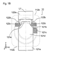
- FIG. 1B is a top view illustrating an inner structure through the resin molded body 11 shown in FIG.1A
- FIG. 3C(a) is a cross-sectional view taken along line A-A of FIG. 1A
- FIG. 3C(b) is a cross-sectional view taken along line B-B of FIG. 1A
- FIG. 3C(c) is a cross-sectional view taken along line C-C of FIG. 1A .
- a first electrically conductive member 121 and a second electrically conductive member 122 which are a pair of positive and negative electrodes are held together by the resin molded body 11 as a whole.
- the resin molded body 11 is arranged with a recess 111, and a plurality of light emitting elements 13 are mounted on the first electrically conductive member 121 which is exposed at the bottom surface in the recess 111.
- Outer surfaces of the resin molded body 11 includes a first outer side surface 112a and a second outer side surface 112b which are at the opposite sides.
- the first electrically conductive member 121 protrudes from the first outer side surface 112a and the second electrically conductive member 122 protrudes from the second outer side surface 112b.
- the recess 111 has a first bottom surface 111a on which the light emitting elements 13 are mounted and a second bottom surface 111b which are arranged at a higher side of the outer periphery defining the first bottom surface 111a.
- the first electrically conductive member 121 has a first bend portion 121b at a position spaced apart from the center line L1.
- the first bend portion 121b is bent upward from the bottom surface side of the recess and a part of the portion further continuous from the first bend portion 121b forms a first exposed portion 121c which is exposed at the second bottom surface 111b.
- arranging the first bend portion at such a position enables efficient extraction of light which is emitted from the light emitting elements, without a necessity of excessive increase in the size of the light emitting device (particularly the size of the light emitting device in the central axis L1 direction).
- each constructional member will be described in detail below.
- the direction perpendicular to the bottom surface of the recess is z-axis direction and in a plane (in xy plane) perpendicular to the z-axis direction, the direction of the center line L1 is y-axis direction and a direction perpendicular to the y-axis direction is x-axis direction.
- the resin molded body arranged with a recess defined by a bottom surface and side surfaces is a member for protecting electronic components, such as a light emitting element and a wire, which are disposed in the recess.
- the resin molded body 11 has an outer shape approximately rectangular in top view and has a recess 111 at approximately the center thereof.
- Examples of the outer shape of the resin molded body 11 include a polygonal shape, a circular shape, an elliptical shape or a shape which is a combination of those, along with such a rectangular shape.
- an electrically conductive member is respectively exposed from a first outer side surface 112a and a second outer side surface 112b which are at the opposite sides.
- opposite sides refers to the surfaces at the opposite sides across the center point of the resin molded body 11 in top view, and include the cases in which, as in a quadrilateral, the first outer side surface and the second outer side surface are two surfaces which are distinguishable from each other with respect to a position, for example, of another interposing outer side surface, and the case in which, as in a circular outer shape, the first side surface and the second side surface are continuous curved surfaces and are indistinguishable as two individual surfaces.
- a recess having an upward opening is arranged.
- a recess 111 having a circular opening is arranged.
- the recess 111 has two bottom surfaces with different heights, a first bottom surface 111a and a second bottom surface 111b which is at a higher position than the first bottom surface 111a.
- the first bottom surface 111a is sufficient to have an area capable of having the light emitting elements 13 mounted thereon, and the second bottom surface 111b is sufficient to have an electrically conductive member exposed with an area capable of having electrically conductive wires connected thereto.
- a single first bottom surface 111a is arranged in a single opening, but it is not limited thereto, two or more first bottom surfaces may be arranged in a single opening, or two or more recesses with different openings may be arranged.
- the shape of the opening in top view may be a circular shape or an elliptical shape, a polygonal shape, or further, a shape of a combination of those shapes.
- the shape of the first bottom surface 111a may be a circular shape as shown in FIG.
- the second bottom surface is sufficiently arranged at a higher side and also at an outer periphery (outer side) of the first bottom surface, and in FIG. 1A , the second bottom surface is arranged at a whole periphery whose inner periphery is the top end of the inner side surface (first inner side surface) 111c of the first bottom surface 111a so as to be in a single plane in parallel to the first bottom surface 111a.
- the angle of the second bottom surface 111b may be different from that of the first bottom surface 111a, and further, a step or unevenness may be formed therein.
- the second bottom surface 111b may be arranged not at the entire periphery of a higher position than the first inner surface 111c, but at a part thereof.
- one or a plurality of two or more second bottom surfaces 111b may be arranged.
- the first exposed portion of electrically conductive member which to be described later is formed at a position spaced apart from the center line L1.
- each of the second bottom surfaces may have the same height, shape, and angle, or may have a height, shape, and angle, of which one of them is different, or all of them are different.
- the second bottom surface 111b is, in FIG. 1A , formed with the resin molded body 11 and the exposed electrically conductive member (first exposed portion 121 c), but it is not limited thereto; the second bottom surface 111b may be formed only with an electrically conductive member.
- the inner side surface (first inner side surface 111 c) of the first bottom surface 111a and the side surface (second inner side surface 111d) arranged at the periphery of the second bottom surface 111b may be formed with the same angle or with different angles, so that the light distribution characteristics of the light from the light emitting elements 13 can be further adjusted. Also, in the case where the second bottom surface 111b is partially formed, the first inner side surface 111c and the second inner side surface 111d may be formed as a surface with no boundary, or may be formed as a continuous surface (a continuous surface without interposing the second bottom surface) with different angles at the same height as the second bottom surface.
- the height of the first inner side surface 111c and the height of the second inner side surface 111d are, in FIG. 1C , arranged so that the height of the first inner side surface 111c is smaller than the height of the second inner side surface 111d, that is, the second bottom surface 111b is closer to the lower side (first bottom surface 111a side) than to the upper side of the recess 111.
- This arrangement allows for a reduction in the length of the electrically conductive wire 14 from the light emitting elements 13, so that adverse effects due to breakage of a wire and such can be reduced.
- the invention is not limited to this embodiment; the first inner side surface 111c and the second inner side surface 111d may have the same height; that is, the second bottom surface 111b may be at a middle between the first bottom surface 111a and the opening (upper surface of the resin molded body), or may be at a position closer to the upper surface side of the recess.
- thermoplastic resin such as aromatic polyamide such as PA6T and PA9T and aromatic polyester resin such as LCP
- thermosetting resin such as epoxy resin composition, silicone resin composition, modified epoxy resin composition such as silicone-modified epoxy resin, modified silicone resin composition such as epoxy-modified silicone resin, polyimide resin composition, and modified polyimide resin composition.
- such a material as described above is mixed with a filler such as fine particles of TiO 2 , SiO 2 , Al 2 O 3 , MgO, MgCO 3 , CaCO 3 , Mg(OH) 2 , Ca(OH) 2 or the like, to adjust its reflectance of light in order to reflect about 60% or more, more preferably about 80% or more, of light from the light emitting elements.
- a filler such as fine particles of TiO 2 , SiO 2 , Al 2 O 3 , MgO, MgCO 3 , CaCO 3 , Mg(OH) 2 , Ca(OH) 2 or the like
- the electrically conductive member is employed to function as a pair of positive and negative electrodes for supplying electric power to a light emitting element, and is prepared by processing a plate-like metal into a desired size and shape and is held together as a whole by a resin molded body.
- the side where the light emitting elements are mounted is indicated as the first electrically conductive member and the side where no light emitting element is mounted is indicated as the second electrically conductive member.
- another electrically conductive member may further be arranged.
- the first electrically conductive member 121 has a bottom surface portion 121d which is at the first bottom surface 111a of the recess 111 and has a light emitting elements 13 mounted thereon, a first bend portion 121b b which is at the inner side of the resin molded body 11 which is a side wall defining the recess 111, and is extended in the x-axis direction from the bottom surface portion 121d and is bent upward (in the z-axis direction) of the recess 111, a first exposed portion 121c which is continuous to the first bend portion 121b and is exposed at the second bottom surface 111b of the recess 111 so that an electrically conductive wire 14 is connected thereto, and a first terminal portion 121a exposed at an outer side of the resin molded body 11 so as to serve as a current supply terminal for electrically connecting to an external current supply member.
- an edge closest to the second outer side surface is indicated as the end portion 121e
- an edge locating on the center line L1 is indicated as the end portion 121 e.
- a first bend portion which extends upward away from the first bottom surface is arranged, and a first exposed portion is arranged continuous from the first bend portion and exposed at the second bottom surface.
- the bottom surface portion 121d of the electrically conductive member which is exposed at the first bottom surface 111a of the recess 111 has an approximately flat surface with an area capable of having the light emitting elements 13 mounted thereon.
- the bottom surface portion 121d is not needed to be entirely one flat surface and may have a step difference (unevenness) and/or a cut-off portion at a position other than the mounting region for the light emitting elements 13.
- a polygonal shape, an elliptical shape, or a shape which is a combination of these shapes may be employed. In the present embodiment, as shown in FIG.
- the bottom surface portion 121d is arranged as approximately the entire surface of the first bottom surface 111a, the region being formed as a single flat surface.
- the light emitting elements 13 are fixed through a bonding member (not shown), and an electrically conductive wire 14 for supplying the current is not connected to the bottom surface portion 121d.
- the first bend portion 121b is for exposing the first electrically conductive member 121, which is a continuous piece, both at the first bottom surface 111a and the second bottom surface 111b which have different heights.
- the first bend portion 121b is arranged so that a part of the first electrically conductive member which is continuous from the bottom surface portion 121d extends upward away from the first bottom surface of the recess 111.
- the position where the first bend portion is extended out may be any position which is spaced apart from the center line L1 which connects the center of the first outer side surface and the center of the second outer side surface.
- the first bend portion 121b is extended from a region, which is in the bottom surface 121d and which is spaced apart from the center line L1, toward a direction different from the direction of the center line L1, more specifically, toward a direction (x-axis direction) perpendicular to the center line L1.
- arranging the first bend portion 121b b extending in a direction different from a direction of the center line L1 makes it possible to avoid a need of unnecessary length to the second electrically conductive member 122, in other words, makes it possible to avoid a need for an excessive size of the resin molded body 11 along the y-axis direction, when arranging a pair of positive and negative electrically conductive members.
- the angle, the length, and the like of the bend of the first bend portion 121b can be adjusted according to the height of the second bottom surface.
- the first bend portion 121b may be formed with a single slope, as shown in FIG. 1C , which does not include a step-like difference, or may be formed with a plurality of slopes each of which having different angles, or may be formed with a step difference.
- the width thereof may be such that, as shown in FIG. 1B , the first bend portion may have a same width from the bottom surface to the first exposed portion, or may have different widths, for example, the width from the bottom surface side toward the first exposed portion may be gradually decreased, or increased, or a step-like difference may be formed.
- first bend portions may be formed with respect to a single first exposed portion.
- first bend portion 121b may be arranged, as shown in FIG. 1B , in the vicinity of the bottom surface portion 221d, or may be arranged at a side close to the first terminal portion 121a. Also, a plurality of two or more first bend portions may be arranged. Further, the first bend portion 121b is preferably embedded in the resin molded body 11. In this case, only a part thereof may be embedded or the entire part thereof may be embedded.
- Embedding in the resin molded body allows an improvement in adhesion between the resin molded body and the electrically conductive member and at the same time enables formation of the first side surface around the light emitting elements only with the resin molded body, which facilitates an adjustment of the light distribution characteristics.
- the first exposed portion 121c is exposed at the second bottom surface 111b and is a portion for connecting an electrically conductive wire thereto, so that it is arranged to expose a sufficient area for connecting the electrically conductive wire.
- the protective element may be arranged at the first bottom surface 111a at which the light emitting elements have also be arranged, but the protective element is preferably mounted on the first exposed portion which is exposed at the second bottom surface 111b.
- the protective element may be arranged on the second exposed portion 122c of the second electrically conductive member, or may be arranged on the first exposed portion 121c of the first electrically conductive member. This arrangement allows reduction in the absorption of light from the light emitting elements 13 by the protective element.
- one pentagonal first exposed portion 121c (shaded area) is arranged and a part thereof is embedded in the second inner side surface 111d. Embedding a part of the first exposed portion 121c makes it possible to prevent separation of the first exposed portion 121c from the resin molded body 11.
- the shape of the first exposed portion is not limited to a pentagonal shape; a polygonal shape, a circular shape, an elliptical shape, or a shape which is a combination of these shapes may be employed.
- the first exposed portion preferably has a flat or recessed shape. Forming a recessed shape enables to provide a resin coating to protect the plating and the wires.
- the size of the first exposed portion can also be selected according to the number of the electrically conductive wires and the like. But the first exposed portion is preferably exposed spaced apart from the first inner side surface 111c, so that bonding can be performed. The same can be applied to the second electrically conductive member.
- the position of the first exposed portion 121c is preferably closer to the first outer side surface 112a than to the end portion 121e of the first electrically conductive member. This arrangement allows the second exposed portion 122c of the second electrically conductive portion to extend close to the light emitting elements, so that the length of the electrically conductive wires 14 can be reduced, which makes it possible to avoid occurrence of breakage of a wire and the like.
- the resin molded body 11 under the first exposed portion 121e is arranged with a recess in lower surface 113 so as to expose a part of the lower surface of the first exposed portion 121c.
- This arrangement is for forming a protruded portion in a mold to press the electrically conductive member at the time of molding, and this arrangement, makes it possible to prevent formation of burrs caused by entering of molten resin at the upper side surface side of the first exposed portion 121c.
- Such a recess in the lower surface is also arranged under the first exposed portion of the second electrically conductive member.
- the first terminal portion 121a is arranged exposed at the outer side surface of the resin molded body 11 and is electrically connected to an external circuit and the like through a solder and the like.
- a part of the first terminal portion 121a exposed at the first outer side surface 112a which is one of the side surfaces of the approximately square resin molded body, is arranged protruding outward beyond the first outer side surface with its height being the same as the bottom surface portion arranged at the bottom surface portion of the recess; that is, the planar metal is extended as it is without being bent.
- the shape of the first terminal portion 121a in top view can be appropriately selected from a circular shape, an elliptic shape, a polygonal shape, or a shape which is a combination of these shapes, as well as an approximately quadrangular shape as shown in FIG. 1A , according to the aim and application.
- the first terminal portion 121a may be arranged not to be protruded from the first outer side surface, that is, it is exposed at the same plane as the first outer side surface.
- the second electrically conductive member which is paired with the first electrically conductive member 121 to form a pair of positive and negative electrodes, is exposed from the second outer side surface 112b.
- the second electrically conductive member has a second bend portion 122b which extends upward away from the first bottom surface at a position spaced apart from the center line L1 which connects the center of the first outer side surface 112a and the center of the second outer side surface 112b, and a second exposed portion 122c which is continuous from the second bend portion 122b and is exposed at the second bottom surface 111b.
- the second electrically conductive member has a second terminal portion 122a, a second bend portion 122b, and a second exposed portion 122c. Since it is not for mounting the light emitting elements, a bottom surface portion which is exposed at the bottom surface 111a of the recess 111 is not provided.
- the second bend portion 122b is, in a region spaced apart from the center line L1, extended in a direction (y-axis direction) parallel to the center line L1. and in this embodiment, two second bend portions 122b are arranged so that the second exposed portion 122c is exposed at two positions interposing the recess 111. In this embodiment, the second bend portions 122b are arranged at positions symmetrical to the center line L1 with the same shape, angle, and size. The number thereof may be one or a plural number of three or more, and in the case of a plural number, different shapes, angles, and/or sizes may be employed. Also, as in the first electrically conductive member, the second bend portion 122b is preferably embedded in the resin molded member 11.
- the second exposed portion 122c is a portion which is exposed at the second bottom surface 111b.
- the second exposed portions 122c are arranged at positions so as to be symmetrical to the center line L1, and the shapes thereof are pentagons mirror-symmetrical with each other.
- the position of the second exposed portion 122c is preferably closer to the first outer side surface 112a than to the end portion 121 e of the first electrically conductive member. This arrangement allows the second exposed portion 122c of the second electrically conductive portion extends close to the light emitting elements, so that the length of the electrically conductive wires 14 can be reduced and which enables to avoid occurrence of disconnection.
- one protective element 16 is mounted, so that the first exposed portion 121c of the first electrically conductive member is arranged exposed at the second bottom surface 111b which is located in the vicinity of the protective element.
- first exposed portion 121c of the first electrically conductive member and the second exposed portion 122c of the second electrically conductive member at positions close to the protective element allows a reduction in the length of the electrically conductive wire 14 connected to the protective element 16.
- the material for the first electrically conductive member and the second electrically conductive member examples include a metal such as copper, aluminum, gold, silver, tungsten, iron, nickel, and cobalt, or iron-nickel alloy, phosphor bronze, copper-iron alloy, molybdenum; these can be used alone or in the form of an alloy.
- the outermost surface (uppermost surface) of the conductive member is preferably provided with a material capable of reflecting light from the light emitting elements; preferred examples thereof include gold, silver, copper, Pt, Pd, Al, W, Mo, Ru, and Rh.
- the reflectivity in a visible range is preferably 70% or more; in such case, Ag, Ru, Rh, Pt, Pd, etc. are preferably used.
- the gloss value is preferably 0.5 or greater, more preferably 1.0 or greater.
- the gloss value shown in the specification is a value measured using a micro surface color difference meter VSR 300A manufactured by NIPPON DENSHOKU INDUSTRIES CO., LTD., under a condition of an illumination angle of 45° and vertical light receiving.
- the outermost surfaces of the bottom surface portion and the first and second exposed portions may be made of respectively different metals such that the outermost surface of the bottom surface portion of the first electrically conductive member is made of Ag or anAg-containing metal, and the outermost surface of the first exposed portion of the first electrically conductive member and the second exposed portion of the second electrically conductive portion are made of a metal which is less susceptible to sulfuration than Ag, for example, Au, an Au alloy, Pd, or a Pd alloy.
- Ag is prone to react under an environment containing, in particular, hydrogen sulfide (H 2 S), among other sulfur-containing gases.
- H 2 S hydrogen sulfide
- Fe and Cu which are used as the base material of the electrically conductive members, are prone to react under an environment containing sulfur oxides (SO x ), particularly one containing sulfur dioxide (SO 2 ).
- SO x sulfur oxides
- SO 2 sulfur dioxide
- the first and second exposed portions, to which the electrically conductive wires are connected are loaded with a mechanical power at the time of connecting the electrically conductive wires, so that the surface quality is different than that of the bottom surface portion. More specifically, the exposed portions and the bottom surface portion have different levels of resistance to sulfur-containing gas (corrosive gas); the first and second exposed portions tend to have lower resistance than that of the bottom surface portion.
- sulfur-containing gas corrosive gas
- the outermost surface of the bottom surface portion of the first electrically conductive member is made of Ag or an Ag-containing metal having high reflectance to the light from the light emitting element
- the outermost surfaces of the first exposed portion of the first electrically conductive portion and the second exposed portion of the second electrically conductive portion are made of a metal which is less susceptible to sulfuration than is Ag, and also has excellent adhesion with the electrically conductive wire, for example, Au, an Au alloy, Pd, or a Pd alloy, in particular Au among those; thus a light emitting element capable of providing high output power and excellent reliability can be obtained.
- first and second exposed portions exposed at the second bottom surface are not directly irradiated with light from the light emitting elements, so that even using a metal having lower reflectance than that of Ag at such positions does not absorb much light and thus the light extracting efficiency is not much reduced.
- a covering layer covering the Ag may be formed.
- an optically transmissive material is preferably used so as not to reduce the reflectance of Ag; examples of such materials include silicon oxide and aluminum oxide.
- a method such as a sputtering method, a CVD method, or an ALD method can be employed, and the thickness of the layer is preferably 1 nm to 200 nm, and more preferably is 5 nm to 100 nm.
- the covering layer may be disposed only at the bottom surface portion or disposed on both the first and second exposed portions of the bottom surface portion. Further, the covering layer may be disposed on the first inner side surface and/or the second inner side surface, and in the case where the light emitting elements and/or the electrically conductive wires are disposed before disposing the covering layer, the covering layer may be disposed on those components.
- the electrically conductive wires that directly or indirectly connect to the electrodes of the light emitting element and the respective electrically conductive members may be made of a metal such as gold, copper, platinum, aluminum or the like, or an alloy of those metals. It is particularly preferable to use gold that has excellent thermal resistance etc.
- a metal such as gold, copper, platinum, aluminum or the like, or an alloy of those metals. It is particularly preferable to use gold that has excellent thermal resistance etc.
- FIG. 1A in the case where the light emitting device 10 has a plurality of light emitting elements 13, joining the electrically conductive wires 14 among the light emitting elements 13 allows the reduction of the joining portions between the electrically conductive members and the electrically conductive wires; in other words, this allows the reduction of the area of the first and second exposed portions.
- FIG. 1A in the case where the light emitting device 10 has a plurality of light emitting elements 13, joining the electrically conductive wires 14 among the light emitting elements 13 allows the reduction of the joining portions between the electrically
- the electrically conductive wires 14 for supplying current to the light emitting elements 13 are arranged to connect the seven light emitting elements, and one of the electrically conductive wires is connected to the first electrically conductive member side and another one of the electrically conductive wires is connected to the second electrically conductive member side. With this arrangement, the area of the first and second exposed portions can be reduced and an unnecessary increase in the size of the resin molded body can be avoided.
- the bonding member used in the present embodiment is for fixing a light emitting element on an electrically conductive member.
- an electrically conductive bonding member examples include a conductive paste of silver, gold, palladium, a solder material such as an Au-Sn eutectic solder, a brazing material such as a low melting temperature metal, or the like.
- An insulating bonding member can be formed using an epoxy resin composite, a silicone resin composite, a polyimide resin composite, a modified resin or a hybrid resin of those, or the like.
- a metal layer with high reflectivity such as Al coating or Ag coating, or a dielectric reflective coating can be disposed on the back surface of the light emitting element.
- the sealing member is a member for covering the light emitting element and/or the electrically conductive members to protect them from dust and moisture and further, from external force.
- the material of the sealing member preferably has optical transmissivity which allows the light from the light emitting element to transmit therethrough, and also has resistance against deterioration by such light.
- Examples of the material thereof include an insulating resin composition having optical transmissivity which allows the light from the light emitting element to transmit therethrough, such as a silicone resin composition, a modified silicone resin composition, an epoxy resin composition, a modified epoxy resin composition, and an acrylic resin composition.
- a silicone resin, an epoxy resin, a urea resin, a fluororesin and a hybrid resin containing at feast one of these resins may be used.
- a coloring agent, a light diffusing agent, a light reflecting material, various fillers, a wavelength converting material (a fluorescent material) or the like may also be contained as required.
- the shape of the outer surface of the sealing member can be selected variously according to the light distribution characteristics or the like. For example, by forming the upper surface in a shape such as a convex lens, a concave lens, or a Fresnel lens, the light distribution characteristics can be adjusted.
- a semiconductor light emitting element of any appropriate wavelength can be employed.
- a light emitting element capable of emitting blue or green light ZnSe, a nitride-based semiconductor (In X Al Y Ga 1-X-Y N, 0 ⁇ X, 0 ⁇ Y, X+Y ⁇ I), or GaP may be employed.
- a light emitting element capable of emitting red light GaAlAs, AllnGaP, or the like may be employed.
- a semiconductor light emitting element made of a material other than the above may also be employed. The composition, color of emitted light, size and number of the light emitting elements to be used can be selected appropriately according to the purpose.
- a nitride semiconductor which is capable of emitting light of a shorter wavelength which is capable of efficiently exciting the fluorescent material is suitably exemplified.
- the emission wavelength can be variously selected by the materials and the content ratio of the mixed crystal of the semiconductor layer.
- a light emitting element capable of emitting ultraviolet light or infrared light can also be employed as well as a light emitting element capable of emitting visible light.
- a light receiving element or the like can be mounted with the light emitting element.
- the light emitting devices according to the devices of the present invention can be utilized in applications such as various indicators, lighting apparatus, displays, backlight light sources for liquid crystal displays, and further, digital video cameras, facsimiles, copiers, image reading systems in scanners or the like, and projector devices.
Landscapes
- Engineering & Computer Science (AREA)
- General Engineering & Computer Science (AREA)
- Led Device Packages (AREA)
Applications Claiming Priority (1)
| Application Number | Priority Date | Filing Date | Title |
|---|---|---|---|
| JP2011020283A JP5941249B2 (ja) | 2011-02-02 | 2011-02-02 | 発光装置 |
Publications (3)
| Publication Number | Publication Date |
|---|---|
| EP2485286A2 true EP2485286A2 (de) | 2012-08-08 |
| EP2485286A3 EP2485286A3 (de) | 2014-08-27 |
| EP2485286B1 EP2485286B1 (de) | 2018-03-21 |
Family
ID=45655324
Family Applications (1)
| Application Number | Title | Priority Date | Filing Date |
|---|---|---|---|
| EP12153247.7A Active EP2485286B1 (de) | 2011-02-02 | 2012-01-31 | Lichtemittierende Vorrichtung |
Country Status (3)
| Country | Link |
|---|---|
| US (2) | US8455915B2 (de) |
| EP (1) | EP2485286B1 (de) |
| JP (1) | JP5941249B2 (de) |
Families Citing this family (4)
| Publication number | Priority date | Publication date | Assignee | Title |
|---|---|---|---|---|
| JP5258666B2 (ja) * | 2009-04-22 | 2013-08-07 | 株式会社半導体エネルギー研究所 | 発光装置の作製方法および成膜用基板 |
| DE102013202904A1 (de) * | 2013-02-22 | 2014-08-28 | Osram Opto Semiconductors Gmbh | Optoelektronisches Halbleiterbauteil und Verfahren zu seiner Herstellung |
| JP6476567B2 (ja) | 2013-03-29 | 2019-03-06 | 日亜化学工業株式会社 | 発光装置 |
| JP6579138B2 (ja) | 2017-03-17 | 2019-09-25 | 日亜化学工業株式会社 | 発光装置 |
Citations (2)
| Publication number | Priority date | Publication date | Assignee | Title |
|---|---|---|---|---|
| JP2006086408A (ja) | 2004-09-17 | 2006-03-30 | Stanley Electric Co Ltd | Led装置 |
| JP2008227485A (ja) | 2007-03-14 | 2008-09-25 | Samsung Electro-Mechanics Co Ltd | Ledパッケージ |
Family Cites Families (11)
| Publication number | Priority date | Publication date | Assignee | Title |
|---|---|---|---|---|
| JP2005085408A (ja) | 2003-09-10 | 2005-03-31 | Kenwood Corp | チェンジャ装置及び記録媒体制御システム |
| KR100593945B1 (ko) * | 2005-05-30 | 2006-06-30 | 삼성전기주식회사 | 고출력 led 패키지 및 그 제조방법 |
| JP5038623B2 (ja) * | 2005-12-27 | 2012-10-03 | 株式会社東芝 | 光半導体装置およびその製造方法 |
| JP2006222454A (ja) * | 2006-05-01 | 2006-08-24 | Toshiba Electronic Engineering Corp | 半導体発光装置および表面実装型パッケージ |
| JP4830768B2 (ja) * | 2006-05-10 | 2011-12-07 | 日亜化学工業株式会社 | 半導体発光装置及び半導体発光装置の製造方法 |
| JP5023781B2 (ja) * | 2006-11-13 | 2012-09-12 | 日亜化学工業株式会社 | 発光装置 |
| JP4795293B2 (ja) * | 2007-03-30 | 2011-10-19 | ローム株式会社 | 半導体発光装置 |
| US8030839B2 (en) * | 2007-11-30 | 2011-10-04 | Nichia Corporation | Phosphor activated with europium, light emitting device using the same and method of manufacturing the phosphor |
| JP5464825B2 (ja) * | 2008-07-23 | 2014-04-09 | ローム株式会社 | Ledモジュール |
| JP2010153666A (ja) * | 2008-12-25 | 2010-07-08 | Showa Denko Kk | 発光装置、発光モジュール、発光装置の製造方法 |
| JP5206598B2 (ja) * | 2009-06-22 | 2013-06-12 | 豊田合成株式会社 | Ledパッケージ |
-
2011
- 2011-02-02 JP JP2011020283A patent/JP5941249B2/ja active Active
-
2012
- 2012-01-31 US US13/362,762 patent/US8455915B2/en active Active
- 2012-01-31 EP EP12153247.7A patent/EP2485286B1/de active Active
-
2013
- 2013-04-25 US US13/870,587 patent/US9091419B2/en active Active
Patent Citations (2)
| Publication number | Priority date | Publication date | Assignee | Title |
|---|---|---|---|---|
| JP2006086408A (ja) | 2004-09-17 | 2006-03-30 | Stanley Electric Co Ltd | Led装置 |
| JP2008227485A (ja) | 2007-03-14 | 2008-09-25 | Samsung Electro-Mechanics Co Ltd | Ledパッケージ |
Also Published As
| Publication number | Publication date |
|---|---|
| US8455915B2 (en) | 2013-06-04 |
| JP2012160625A (ja) | 2012-08-23 |
| US9091419B2 (en) | 2015-07-28 |
| EP2485286B1 (de) | 2018-03-21 |
| EP2485286A3 (de) | 2014-08-27 |
| JP5941249B2 (ja) | 2016-06-29 |
| US20120228662A1 (en) | 2012-09-13 |
| US20130235599A1 (en) | 2013-09-12 |
Similar Documents
| Publication | Publication Date | Title |
|---|---|---|
| TWI462343B (zh) | 發光裝置 | |
| US10636945B2 (en) | Method of manufacturing light emitting device including metal patterns and cut-out section | |
| US7964892B2 (en) | Light emitting device | |
| EP1998380A2 (de) | Lichtemittierendes Halbleiterbauelement | |
| JPWO2012157644A1 (ja) | 発光装置及びその製造方法 | |
| JP2014197674A (ja) | リードフレーム及び半導体装置 | |
| JP5365252B2 (ja) | 光半導体装置及びその製造方法 | |
| US20140117403A1 (en) | Light emitting device package and light emitting device | |
| US9425373B2 (en) | Light emitting module | |
| US9246074B2 (en) | Light emitting device | |
| CN103545431B (zh) | 发光装置 | |
| US9091419B2 (en) | Light emitting device | |
| JP5849694B2 (ja) | 発光装置及びその製造方法 | |
| US20230095815A1 (en) | Light-emitting device and method of manufacturing the same | |
| JP5071069B2 (ja) | 発光装置 | |
| JP5682341B2 (ja) | 発光装置及びその製造方法 | |
| JP2016119464A (ja) | 発光装置 | |
| US11506361B2 (en) | Light emitting device and light source device | |
| CN103227264B (zh) | 发光装置 | |
| JP7436828B2 (ja) | 発光装置 | |
| JP7057513B2 (ja) | 発光装置 | |
| JP6809522B2 (ja) | 発光装置 | |
| JP2015195416A (ja) | 発光装置 |
Legal Events
| Date | Code | Title | Description |
|---|---|---|---|
| PUAI | Public reference made under article 153(3) epc to a published international application that has entered the european phase |
Free format text: ORIGINAL CODE: 0009012 |
|
| AK | Designated contracting states |
Kind code of ref document: A2 Designated state(s): AL AT BE BG CH CY CZ DE DK EE ES FI FR GB GR HR HU IE IS IT LI LT LU LV MC MK MT NL NO PL PT RO RS SE SI SK SM TR |
|
| AX | Request for extension of the european patent |
Extension state: BA ME |
|
| PUAL | Search report despatched |
Free format text: ORIGINAL CODE: 0009013 |
|
| AK | Designated contracting states |
Kind code of ref document: A3 Designated state(s): AL AT BE BG CH CY CZ DE DK EE ES FI FR GB GR HR HU IE IS IT LI LT LU LV MC MK MT NL NO PL PT RO RS SE SI SK SM TR |
|
| AX | Request for extension of the european patent |
Extension state: BA ME |
|
| RIC1 | Information provided on ipc code assigned before grant |
Ipc: H01L 33/62 20100101AFI20140723BHEP |
|
| 17P | Request for examination filed |
Effective date: 20150227 |
|
| RBV | Designated contracting states (corrected) |
Designated state(s): AL AT BE BG CH CY CZ DE DK EE ES FI FR GB GR HR HU IE IS IT LI LT LU LV MC MK MT NL NO PL PT RO RS SE SI SK SM TR |
|
| STAA | Information on the status of an ep patent application or granted ep patent |
Free format text: STATUS: EXAMINATION IS IN PROGRESS |
|
| 17Q | First examination report despatched |
Effective date: 20161222 |
|
| GRAP | Despatch of communication of intention to grant a patent |
Free format text: ORIGINAL CODE: EPIDOSNIGR1 |
|
| STAA | Information on the status of an ep patent application or granted ep patent |
Free format text: STATUS: GRANT OF PATENT IS INTENDED |
|
| RIC1 | Information provided on ipc code assigned before grant |
Ipc: H01L 33/62 20100101AFI20170919BHEP Ipc: H01L 33/48 20100101ALN20170919BHEP |
|
| INTG | Intention to grant announced |
Effective date: 20171005 |
|
| GRAS | Grant fee paid |
Free format text: ORIGINAL CODE: EPIDOSNIGR3 |
|
| GRAA | (expected) grant |
Free format text: ORIGINAL CODE: 0009210 |
|
| STAA | Information on the status of an ep patent application or granted ep patent |
Free format text: STATUS: THE PATENT HAS BEEN GRANTED |
|
| AK | Designated contracting states |
Kind code of ref document: B1 Designated state(s): AL AT BE BG CH CY CZ DE DK EE ES FI FR GB GR HR HU IE IS IT LI LT LU LV MC MK MT NL NO PL PT RO RS SE SI SK SM TR |
|
| REG | Reference to a national code |
Ref country code: GB Ref legal event code: FG4D |
|
| REG | Reference to a national code |
Ref country code: CH Ref legal event code: EP |
|
| REG | Reference to a national code |
Ref country code: AT Ref legal event code: REF Ref document number: 981967 Country of ref document: AT Kind code of ref document: T Effective date: 20180415 |
|
| REG | Reference to a national code |
Ref country code: IE Ref legal event code: FG4D |
|
| REG | Reference to a national code |
Ref country code: DE Ref legal event code: R096 Ref document number: 602012044107 Country of ref document: DE |
|
| REG | Reference to a national code |
Ref country code: NL Ref legal event code: MP Effective date: 20180321 |
|
| PG25 | Lapsed in a contracting state [announced via postgrant information from national office to epo] |
Ref country code: NO Free format text: LAPSE BECAUSE OF FAILURE TO SUBMIT A TRANSLATION OF THE DESCRIPTION OR TO PAY THE FEE WITHIN THE PRESCRIBED TIME-LIMIT Effective date: 20180621 Ref country code: FI Free format text: LAPSE BECAUSE OF FAILURE TO SUBMIT A TRANSLATION OF THE DESCRIPTION OR TO PAY THE FEE WITHIN THE PRESCRIBED TIME-LIMIT Effective date: 20180321 Ref country code: CY Free format text: LAPSE BECAUSE OF FAILURE TO SUBMIT A TRANSLATION OF THE DESCRIPTION OR TO PAY THE FEE WITHIN THE PRESCRIBED TIME-LIMIT Effective date: 20180321 Ref country code: HR Free format text: LAPSE BECAUSE OF FAILURE TO SUBMIT A TRANSLATION OF THE DESCRIPTION OR TO PAY THE FEE WITHIN THE PRESCRIBED TIME-LIMIT Effective date: 20180321 Ref country code: LT Free format text: LAPSE BECAUSE OF FAILURE TO SUBMIT A TRANSLATION OF THE DESCRIPTION OR TO PAY THE FEE WITHIN THE PRESCRIBED TIME-LIMIT Effective date: 20180321 |
|
| REG | Reference to a national code |
Ref country code: LT Ref legal event code: MG4D |
|
| REG | Reference to a national code |
Ref country code: AT Ref legal event code: MK05 Ref document number: 981967 Country of ref document: AT Kind code of ref document: T Effective date: 20180321 |
|
| PG25 | Lapsed in a contracting state [announced via postgrant information from national office to epo] |
Ref country code: BG Free format text: LAPSE BECAUSE OF FAILURE TO SUBMIT A TRANSLATION OF THE DESCRIPTION OR TO PAY THE FEE WITHIN THE PRESCRIBED TIME-LIMIT Effective date: 20180621 Ref country code: RS Free format text: LAPSE BECAUSE OF FAILURE TO SUBMIT A TRANSLATION OF THE DESCRIPTION OR TO PAY THE FEE WITHIN THE PRESCRIBED TIME-LIMIT Effective date: 20180321 Ref country code: SE Free format text: LAPSE BECAUSE OF FAILURE TO SUBMIT A TRANSLATION OF THE DESCRIPTION OR TO PAY THE FEE WITHIN THE PRESCRIBED TIME-LIMIT Effective date: 20180321 Ref country code: LV Free format text: LAPSE BECAUSE OF FAILURE TO SUBMIT A TRANSLATION OF THE DESCRIPTION OR TO PAY THE FEE WITHIN THE PRESCRIBED TIME-LIMIT Effective date: 20180321 Ref country code: GR Free format text: LAPSE BECAUSE OF FAILURE TO SUBMIT A TRANSLATION OF THE DESCRIPTION OR TO PAY THE FEE WITHIN THE PRESCRIBED TIME-LIMIT Effective date: 20180622 |
|
| PG25 | Lapsed in a contracting state [announced via postgrant information from national office to epo] |
Ref country code: EE Free format text: LAPSE BECAUSE OF FAILURE TO SUBMIT A TRANSLATION OF THE DESCRIPTION OR TO PAY THE FEE WITHIN THE PRESCRIBED TIME-LIMIT Effective date: 20180321 Ref country code: PL Free format text: LAPSE BECAUSE OF FAILURE TO SUBMIT A TRANSLATION OF THE DESCRIPTION OR TO PAY THE FEE WITHIN THE PRESCRIBED TIME-LIMIT Effective date: 20180321 Ref country code: ES Free format text: LAPSE BECAUSE OF FAILURE TO SUBMIT A TRANSLATION OF THE DESCRIPTION OR TO PAY THE FEE WITHIN THE PRESCRIBED TIME-LIMIT Effective date: 20180321 Ref country code: NL Free format text: LAPSE BECAUSE OF FAILURE TO SUBMIT A TRANSLATION OF THE DESCRIPTION OR TO PAY THE FEE WITHIN THE PRESCRIBED TIME-LIMIT Effective date: 20180321 Ref country code: RO Free format text: LAPSE BECAUSE OF FAILURE TO SUBMIT A TRANSLATION OF THE DESCRIPTION OR TO PAY THE FEE WITHIN THE PRESCRIBED TIME-LIMIT Effective date: 20180321 Ref country code: AL Free format text: LAPSE BECAUSE OF FAILURE TO SUBMIT A TRANSLATION OF THE DESCRIPTION OR TO PAY THE FEE WITHIN THE PRESCRIBED TIME-LIMIT Effective date: 20180321 |
|
| PG25 | Lapsed in a contracting state [announced via postgrant information from national office to epo] |
Ref country code: SK Free format text: LAPSE BECAUSE OF FAILURE TO SUBMIT A TRANSLATION OF THE DESCRIPTION OR TO PAY THE FEE WITHIN THE PRESCRIBED TIME-LIMIT Effective date: 20180321 Ref country code: SM Free format text: LAPSE BECAUSE OF FAILURE TO SUBMIT A TRANSLATION OF THE DESCRIPTION OR TO PAY THE FEE WITHIN THE PRESCRIBED TIME-LIMIT Effective date: 20180321 Ref country code: AT Free format text: LAPSE BECAUSE OF FAILURE TO SUBMIT A TRANSLATION OF THE DESCRIPTION OR TO PAY THE FEE WITHIN THE PRESCRIBED TIME-LIMIT Effective date: 20180321 Ref country code: CZ Free format text: LAPSE BECAUSE OF FAILURE TO SUBMIT A TRANSLATION OF THE DESCRIPTION OR TO PAY THE FEE WITHIN THE PRESCRIBED TIME-LIMIT Effective date: 20180321 |
|
| PG25 | Lapsed in a contracting state [announced via postgrant information from national office to epo] |
Ref country code: PT Free format text: LAPSE BECAUSE OF FAILURE TO SUBMIT A TRANSLATION OF THE DESCRIPTION OR TO PAY THE FEE WITHIN THE PRESCRIBED TIME-LIMIT Effective date: 20180723 |
|
| REG | Reference to a national code |
Ref country code: DE Ref legal event code: R097 Ref document number: 602012044107 Country of ref document: DE |
|
| PLBE | No opposition filed within time limit |
Free format text: ORIGINAL CODE: 0009261 |
|
| STAA | Information on the status of an ep patent application or granted ep patent |
Free format text: STATUS: NO OPPOSITION FILED WITHIN TIME LIMIT |
|
| PG25 | Lapsed in a contracting state [announced via postgrant information from national office to epo] |
Ref country code: DK Free format text: LAPSE BECAUSE OF FAILURE TO SUBMIT A TRANSLATION OF THE DESCRIPTION OR TO PAY THE FEE WITHIN THE PRESCRIBED TIME-LIMIT Effective date: 20180321 |
|
| 26N | No opposition filed |
Effective date: 20190102 |
|
| PG25 | Lapsed in a contracting state [announced via postgrant information from national office to epo] |
Ref country code: IT Free format text: LAPSE BECAUSE OF FAILURE TO SUBMIT A TRANSLATION OF THE DESCRIPTION OR TO PAY THE FEE WITHIN THE PRESCRIBED TIME-LIMIT Effective date: 20180321 |
|
| PG25 | Lapsed in a contracting state [announced via postgrant information from national office to epo] |
Ref country code: SI Free format text: LAPSE BECAUSE OF FAILURE TO SUBMIT A TRANSLATION OF THE DESCRIPTION OR TO PAY THE FEE WITHIN THE PRESCRIBED TIME-LIMIT Effective date: 20180321 |
|
| PG25 | Lapsed in a contracting state [announced via postgrant information from national office to epo] |
Ref country code: MC Free format text: LAPSE BECAUSE OF FAILURE TO SUBMIT A TRANSLATION OF THE DESCRIPTION OR TO PAY THE FEE WITHIN THE PRESCRIBED TIME-LIMIT Effective date: 20180321 |
|
| REG | Reference to a national code |
Ref country code: CH Ref legal event code: PL |
|
| PG25 | Lapsed in a contracting state [announced via postgrant information from national office to epo] |
Ref country code: LU Free format text: LAPSE BECAUSE OF NON-PAYMENT OF DUE FEES Effective date: 20190131 |
|
| REG | Reference to a national code |
Ref country code: BE Ref legal event code: MM Effective date: 20190131 |
|
| REG | Reference to a national code |
Ref country code: IE Ref legal event code: MM4A |
|
| PG25 | Lapsed in a contracting state [announced via postgrant information from national office to epo] |
Ref country code: BE Free format text: LAPSE BECAUSE OF NON-PAYMENT OF DUE FEES Effective date: 20190131 |
|
| PG25 | Lapsed in a contracting state [announced via postgrant information from national office to epo] |
Ref country code: CH Free format text: LAPSE BECAUSE OF NON-PAYMENT OF DUE FEES Effective date: 20190131 Ref country code: LI Free format text: LAPSE BECAUSE OF NON-PAYMENT OF DUE FEES Effective date: 20190131 |
|
| PG25 | Lapsed in a contracting state [announced via postgrant information from national office to epo] |
Ref country code: IE Free format text: LAPSE BECAUSE OF NON-PAYMENT OF DUE FEES Effective date: 20190131 |
|
| PG25 | Lapsed in a contracting state [announced via postgrant information from national office to epo] |
Ref country code: TR Free format text: LAPSE BECAUSE OF FAILURE TO SUBMIT A TRANSLATION OF THE DESCRIPTION OR TO PAY THE FEE WITHIN THE PRESCRIBED TIME-LIMIT Effective date: 20180321 |
|
| PG25 | Lapsed in a contracting state [announced via postgrant information from national office to epo] |
Ref country code: MT Free format text: LAPSE BECAUSE OF NON-PAYMENT OF DUE FEES Effective date: 20190131 |
|
| PG25 | Lapsed in a contracting state [announced via postgrant information from national office to epo] |
Ref country code: IS Free format text: LAPSE BECAUSE OF FAILURE TO SUBMIT A TRANSLATION OF THE DESCRIPTION OR TO PAY THE FEE WITHIN THE PRESCRIBED TIME-LIMIT Effective date: 20180721 |
|
| PG25 | Lapsed in a contracting state [announced via postgrant information from national office to epo] |
Ref country code: HU Free format text: LAPSE BECAUSE OF FAILURE TO SUBMIT A TRANSLATION OF THE DESCRIPTION OR TO PAY THE FEE WITHIN THE PRESCRIBED TIME-LIMIT; INVALID AB INITIO Effective date: 20120131 |
|
| PG25 | Lapsed in a contracting state [announced via postgrant information from national office to epo] |
Ref country code: MK Free format text: LAPSE BECAUSE OF FAILURE TO SUBMIT A TRANSLATION OF THE DESCRIPTION OR TO PAY THE FEE WITHIN THE PRESCRIBED TIME-LIMIT Effective date: 20180321 |
|
| P01 | Opt-out of the competence of the unified patent court (upc) registered |
Effective date: 20230522 |
|
| REG | Reference to a national code |
Ref country code: DE Ref legal event code: R079 Ref document number: 602012044107 Country of ref document: DE Free format text: PREVIOUS MAIN CLASS: H01L0033620000 Ipc: H10H0020857000 |
|
| PGFP | Annual fee paid to national office [announced via postgrant information from national office to epo] |
Ref country code: GB Payment date: 20251211 Year of fee payment: 15 |
|
| PGFP | Annual fee paid to national office [announced via postgrant information from national office to epo] |
Ref country code: FR Payment date: 20251128 Year of fee payment: 15 |
|
| PGFP | Annual fee paid to national office [announced via postgrant information from national office to epo] |
Ref country code: DE Payment date: 20251210 Year of fee payment: 15 |