EP2463401B1 - Vorrichtung zur Herstellung einer gerichteten Schicht mittels Kathodenzerstäubung und Verwendung derselben - Google Patents
Vorrichtung zur Herstellung einer gerichteten Schicht mittels Kathodenzerstäubung und Verwendung derselben Download PDFInfo
- Publication number
- EP2463401B1 EP2463401B1 EP12001531.8A EP12001531A EP2463401B1 EP 2463401 B1 EP2463401 B1 EP 2463401B1 EP 12001531 A EP12001531 A EP 12001531A EP 2463401 B1 EP2463401 B1 EP 2463401B1
- Authority
- EP
- European Patent Office
- Prior art keywords
- plates
- collimator
- substrate surface
- target
- substrate
- Prior art date
- Legal status (The legal status is an assumption and is not a legal conclusion. Google has not performed a legal analysis and makes no representation as to the accuracy of the status listed.)
- Not-in-force
Links
Images
Classifications
-
- C—CHEMISTRY; METALLURGY
- C23—COATING METALLIC MATERIAL; COATING MATERIAL WITH METALLIC MATERIAL; CHEMICAL SURFACE TREATMENT; DIFFUSION TREATMENT OF METALLIC MATERIAL; COATING BY VACUUM EVAPORATION, BY SPUTTERING, BY ION IMPLANTATION OR BY CHEMICAL VAPOUR DEPOSITION, IN GENERAL; INHIBITING CORROSION OF METALLIC MATERIAL OR INCRUSTATION IN GENERAL
- C23C—COATING METALLIC MATERIAL; COATING MATERIAL WITH METALLIC MATERIAL; SURFACE TREATMENT OF METALLIC MATERIAL BY DIFFUSION INTO THE SURFACE, BY CHEMICAL CONVERSION OR SUBSTITUTION; COATING BY VACUUM EVAPORATION, BY SPUTTERING, BY ION IMPLANTATION OR BY CHEMICAL VAPOUR DEPOSITION, IN GENERAL
- C23C14/00—Coating by vacuum evaporation, by sputtering or by ion implantation of the coating forming material
- C23C14/22—Coating by vacuum evaporation, by sputtering or by ion implantation of the coating forming material characterised by the process of coating
- C23C14/34—Sputtering
-
- G—PHYSICS
- G11—INFORMATION STORAGE
- G11B—INFORMATION STORAGE BASED ON RELATIVE MOVEMENT BETWEEN RECORD CARRIER AND TRANSDUCER
- G11B5/00—Recording by magnetisation or demagnetisation of a record carrier; Reproducing by magnetic means; Record carriers therefor
- G11B5/84—Processes or apparatus specially adapted for manufacturing record carriers
- G11B5/851—Coating a support with a magnetic layer by sputtering
-
- H—ELECTRICITY
- H01—ELECTRIC ELEMENTS
- H01J—ELECTRIC DISCHARGE TUBES OR DISCHARGE LAMPS
- H01J37/00—Discharge tubes with provision for introducing objects or material to be exposed to the discharge, e.g. for the purpose of examination or processing thereof
- H01J37/32—Gas-filled discharge tubes
- H01J37/34—Gas-filled discharge tubes operating with cathodic sputtering
- H01J37/3411—Constructional aspects of the reactor
- H01J37/3447—Collimators, shutters, apertures
-
- H—ELECTRICITY
- H10—SEMICONDUCTOR DEVICES; ELECTRIC SOLID-STATE DEVICES NOT OTHERWISE PROVIDED FOR
- H10P—GENERIC PROCESSES OR APPARATUS FOR THE MANUFACTURE OR TREATMENT OF DEVICES COVERED BY CLASS H10
- H10P14/00—Formation of materials, e.g. in the shape of layers or pillars
- H10P14/20—Formation of materials, e.g. in the shape of layers or pillars of semiconductor materials
- H10P14/22—Formation of materials, e.g. in the shape of layers or pillars of semiconductor materials using physical deposition, e.g. vacuum deposition or sputtering
-
- H—ELECTRICITY
- H10—SEMICONDUCTOR DEVICES; ELECTRIC SOLID-STATE DEVICES NOT OTHERWISE PROVIDED FOR
- H10P—GENERIC PROCESSES OR APPARATUS FOR THE MANUFACTURE OR TREATMENT OF DEVICES COVERED BY CLASS H10
- H10P72/00—Handling or holding of wafers, substrates or devices during manufacture or treatment thereof
- H10P72/04—Apparatus for manufacture or treatment
- H10P72/0451—Apparatus for manufacturing or treating in a plurality of work-stations
- H10P72/0468—Apparatus for manufacturing or treating in a plurality of work-stations comprising a chamber adapted to a particular process
Definitions
- the invention relates to a device for producing a directional layer on a flat substrate surface with a respectively lying in the same excellent direction by means of sputtering.
- Such layers are often magnetic layers or carrier layers for magnetic layers having a preferred direction of magnetization. They are mainly used in storage devices for data processing equipment, e.g. in read / write heads for hard disks and MRAMs.
- the invention also relates to a corresponding use of the device.
- a directional magnetic layer is produced on a planar substrate surface which is easier to magnetize in a specific, substantially constant, direction (so-called easy axis) than in other directions, in particular normal to the excellent direction.
- electromagnets are arranged below the substrate, which generate a magnetic field, on whose field lines the particles impinging on the substrate surface align magnetically, such that the excellent direction is parallel to the field lines.
- a similar device, in which permanent magnets are used, is in US 2003/0140 084 A1 described.
- a grounded collimator disposed between the target and the substrate is used to limit the angle of incidence of particles on the substrate surface by trapping particles with angles more deviating from the surface normal and also serves to keep the plasma away from the substrate.
- WO 96/08 817 A1 Another similar device just described is off WO 96/08 817 A1 known. Again, a collimator is used whose aspect ratio is used to control parameters of the magnetic layer so that the orientation of the crystals occurs either in the plane of the substrate surface or normal to it. In the former case, however, no excellent direction is sought within said plane.
- US 5 584 973 A a similar device known in which in order to ensure a sufficient coating in deep, deep contact holes of Surface of the angle of incidence is limited by a arranged between a target and a substrate collimator, which comprises two closely superposed flocks of parallel, normal to the substrate surface facing plates that cross each other at right angles.
- the plates can be rotated, for example, about central longitudinal axes. Turning the plates through 180 ° between two sputtering operations with different materials will reduce contamination.
- a collimator is provided, which preferably forms cells of hexagonal cross-section.
- the cells may have different lengths and diameters, eg, the top of the collimator may be stepped such that the length of the cells decreases toward outer edges.
- US 2003/062 260 A1 serves to apply a directional support layer for producing a magnetic layer for a storage medium on a surface of a substrate, using three targets and a radial plate collimator arranged between them and the substrate, which rotates about a central axis to avoid shadows. If the plates are parallel to the axis, a magnetic layer with an excellent direction is produced, which is for example directed radially, depending on the type of carrier layer. The plates can also be inclined in the same direction with respect to the axis. The device is not suitable for the production of a directional layer with a constant excellent direction.
- the invention is based on the object to provide a generic device with which a layer with constant excellent direction can be applied, in which the latter is adhered to the entire substrate surface with high accuracy and differences in the thickness of the layer are relatively small.
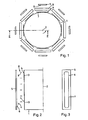
- the device according to Fig. 1-3 is arranged in a vacuum chamber (not shown). It has a cylindrical basket 1 which is rotatable about an axis 2 and carries on its outer side brackets on which substrates 3 are attached with outwardly facing flat substrate surfaces 4.
- the substrates 3 may be about 200 mm diameter discs, which are zersägt after their completion, for example, for the production of components for read / write heads.
- the basket 1 is surrounded at some distance by targets 5, which are formed as elongated vertical plates which face the axis 2 a target surface 6.
- the targets 5 are formed in a known manner as magnetron targets, ie behind the target surface 6 magnets are arranged, which in the region of the target surface 6 about a closed curve 7 (FIG. Fig. 3 ) generate concentrated magnetic field, so that the target 5 is removed above all in this area and form corresponding erosion ditches in the target surface 6.
- each of the targets 5 and the basket 1 arranged as a collimator collimator 8, which as a comb collimator with a plurality of spaced congruent superimposed parallel rectangular plates 9, which consist for example of aluminum , is trained.
- the distance between the target surface 6 and the substrate surface 4 may be, for example 75mm, the distance between the collimator 8 and substrate surface 4 30mm, the length of the plates 9 10mm and their distance 50mm.
- the substrates 3 are vapor-coated with target material in a manner known per se during a coating time by means of cathode sputtering, while the basket 1 is slowly and uniformly, e.g. is rotated with 0.1U / s.
- the basket 1 is slowly and uniformly, e.g. is rotated with 0.1U / s.
- the final desired result may be, for example, a soft magnetic layer on the substrate surface which has a preferred direction of magnetization, ie a direction in which the layer is already magnetizable by a relatively small magnetic field (so-called easy axis) while in the direction normal to it much higher magnetic field is required (so-called hard axis).
- targets 5 which consist essentially of the soft-magnetic material such as nickel-iron, eg NiFe21 or cobalt-iron and thus a layer of the soft-magnetic material is sputtered directly onto a base layer forming the substrate surface 4 which has a preferred direction of magnetization.
- Another way to apply a magnetic layer with a preferred direction of magnetization on the substrate surface 4 is to first form a directed carrier layer, e.g. of chromium, vanadium or tungsten and then on this support layer, to apply a layer of magnetic material whose preferred direction of magnetization is then determined by the excellent direction of the support layer, usually by adjusting depending on the materials used in parallel or normal to the same , In this case, when applying the magnetic layer, which usually also takes place by sputtering, no special measures for producing an excellent direction are required, although they can be additionally taken.
- a directed carrier layer e.g. of chromium, vanadium or tungsten
- the formation of the preferred direction of magnetization can be assisted in a manner known per se by applying to the vapor deposition of the magnetic layer a magnetic field which is effective in the area of the substrate surface 4, e.g. its projection on the substrate surface in each target point thereof coincides with the preferred magnetization direction.
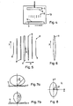
- FIG. 4 Another inventive device is in Fig. 4 shown.
- the substrate 3 is stationarily arranged at the bottom of a vacuum chamber 10 in such a way that the planar substrate surface 4 faces upwards.
- a target 5 is attached with a pointing down against the substrate 3 target surface 6.
- the substrate 3 and the target 5 are disk-shaped.
- the turn behind the target surface 6 arranged magnets are rotatable.
- a shielding device is again arranged, which in turn is designed as a collimator 8.
- the collimator 8 is again designed as a comb collimator, which ( Fig. 5 ) composed of parallel, flat plates 9, which may again consist of aluminum and are directed normal to the substrate surface 4, that is vertical in the present case. Parallel to the substrate surface 4, they are aligned in a y-direction. The distances at which adjacent plates 9 follow each other in a normal to the y-direction, also parallel to the substrate plane x-direction, preferably increase slowly from the center to the outer edges.
- the plates 9 can have different lengths or average lengths and / or thicknesses or average thicknesses, preferably such that the length and / or the thickness generally decrease in the x-direction from a center to both outer edges. In the case of over the surface, in particular in the y-direction, ie parallel to the substrate surface 4 changing thickness of the single plate 9, this also preferably decreases from the center to both outer edges, as in Fig. 6 is shown.
- the collimator 8 is rotatable relative to the substrate 3 about a central axis 11, whereby it is usually easier to rotatably support the substrate 3 while the collimator 8 is fixedly mounted.
- the plates 9 are arranged so that each of the plates 9, with the exception of one edge plate, is brought to a position approximately mid-way through a rotation through 180 °, by which the collimator 8 is changed from a first to a second position
- cathode sputtering is again used in a manner known per se, target material in this case being removed on the target surface 6 along a heart-shaped curve.
- curved substrate surfaces can be coated and the excellent direction can be a - preferably continuous - function of the place, ie depend on the target point.
- the incidence of particles on the substrate surface is controlled so that the temporal average in sum dominate those directions of incidence whose projection on the tangential surface of the substrate surface - which in the case of a planar substrate surface coincides with this - at the respective target point the excellent direction.
- the excellent direction is defined unsigned, so it comes It does not matter whether the invasion is by one side or the other.
- the substrate may perform a movement relative to the target or targets such that certain directions of incidence whose projection onto the tangential surface is close to the pointed direction are preferred.
- the movement can also be non-uniform and / or intermittent and it can additionally the performance of the device, ie the density of the outgoing from the target particle flow with the position of the substrate to the target are selectively changed, such that they are parallel with predominantly flat particle incidence is particularly high to the excellent direction.
- Both approaches can, as in the first embodiment according to Fig. 1-3 can also be used in combination, such as by slowing down or stopping the rotation of the basket 1 when the substrates 3 are approximately midway between two adjacent targets 5. In addition, then the power can be increased.
- the shielding means should then be designed and arranged such that the paths of the particles which follow substantially straight lines connecting a point of the target surface to the target point on the substrate surface collide with the shielding means, ie the particles Otherwise, if they arrive at the target point from a direction whose projection is on the tangential surface outside the preferred angle range, they will be intercepted. At a minimum, this should be predominantly the case over coating time and weighted average of the steepness of the incidence, ie the angle ⁇ . In this case, it may also be necessary to take into account that the target surface has different active regions, that is to say that the particles originate predominantly from a relatively small part thereof, for example in the first exemplary embodiment from the surroundings of the curve 7.
- a magnetic field may also be applied in the region of the substrate, but in most cases this is not necessary.
Landscapes
- Chemical & Material Sciences (AREA)
- Engineering & Computer Science (AREA)
- Physics & Mathematics (AREA)
- Plasma & Fusion (AREA)
- Analytical Chemistry (AREA)
- Chemical Kinetics & Catalysis (AREA)
- Materials Engineering (AREA)
- Mechanical Engineering (AREA)
- Metallurgy (AREA)
- Organic Chemistry (AREA)
- Physical Vapour Deposition (AREA)
- Manufacturing Of Magnetic Record Carriers (AREA)
Applications Claiming Priority (2)
| Application Number | Priority Date | Filing Date | Title |
|---|---|---|---|
| US88308607P | 2007-01-02 | 2007-01-02 | |
| EP07845644A EP2106457A1 (de) | 2007-01-02 | 2007-12-24 | Verfahren zur herstellung einer gerichteten schicht mittels kathodenzerstäubung und vorrichtung zur durchführung des verfahrens |
Related Parent Applications (1)
| Application Number | Title | Priority Date | Filing Date |
|---|---|---|---|
| EP07845644.9 Division | 2007-12-24 |
Publications (2)
| Publication Number | Publication Date |
|---|---|
| EP2463401A1 EP2463401A1 (de) | 2012-06-13 |
| EP2463401B1 true EP2463401B1 (de) | 2013-07-24 |
Family
ID=39144429
Family Applications (2)
| Application Number | Title | Priority Date | Filing Date |
|---|---|---|---|
| EP12001531.8A Not-in-force EP2463401B1 (de) | 2007-01-02 | 2007-12-24 | Vorrichtung zur Herstellung einer gerichteten Schicht mittels Kathodenzerstäubung und Verwendung derselben |
| EP07845644A Withdrawn EP2106457A1 (de) | 2007-01-02 | 2007-12-24 | Verfahren zur herstellung einer gerichteten schicht mittels kathodenzerstäubung und vorrichtung zur durchführung des verfahrens |
Family Applications After (1)
| Application Number | Title | Priority Date | Filing Date |
|---|---|---|---|
| EP07845644A Withdrawn EP2106457A1 (de) | 2007-01-02 | 2007-12-24 | Verfahren zur herstellung einer gerichteten schicht mittels kathodenzerstäubung und vorrichtung zur durchführung des verfahrens |
Country Status (7)
| Country | Link |
|---|---|
| US (1) | US9587306B2 (enExample) |
| EP (2) | EP2463401B1 (enExample) |
| JP (1) | JP5185285B2 (enExample) |
| KR (1) | KR101761401B1 (enExample) |
| CN (2) | CN101627146A (enExample) |
| TW (1) | TWI457453B (enExample) |
| WO (1) | WO2008080244A1 (enExample) |
Families Citing this family (20)
| Publication number | Priority date | Publication date | Assignee | Title |
|---|---|---|---|---|
| TW201209205A (en) * | 2010-07-09 | 2012-03-01 | Oc Oerlikon Balzers Ag | Magnetron sputtering apparatus |
| CN103147055A (zh) * | 2013-03-04 | 2013-06-12 | 电子科技大学 | 一种直列多靶磁控溅射镀膜装置 |
| DE102014108348A1 (de) | 2014-06-13 | 2015-12-17 | Osram Opto Semiconductors Gmbh | Verfahren zur Herstellung einer Beschichtung sowie optoelektronisches Halbleiterbauteil mit einer Beschichtung |
| US9887073B2 (en) * | 2015-02-13 | 2018-02-06 | Taiwan Semiconductor Manufacturing Co., Ltd. | Physical vapor deposition system and physical vapor depositing method using the same |
| US10063210B2 (en) | 2015-10-14 | 2018-08-28 | Qorvo Us, Inc. | Methods for producing piezoelectric bulk and crystalline seed layers of different C-axis orientation distributions |
| US10866216B2 (en) | 2015-12-15 | 2020-12-15 | Qorvo Biotechnologies, Llc | Temperature compensation and operational configuration for bulk acoustic wave resonator devices |
| JP2020517832A (ja) * | 2017-04-27 | 2020-06-18 | エヴァテック・アーゲー | 軟磁性多層堆積装置、製造の方法、および磁性多層体 |
| US11476099B2 (en) | 2018-02-13 | 2022-10-18 | Evatec Ag | Methods of and apparatus for magnetron sputtering |
| US11824511B2 (en) | 2018-03-21 | 2023-11-21 | Qorvo Us, Inc. | Method for manufacturing piezoelectric bulk layers with tilted c-axis orientation |
| US11381212B2 (en) | 2018-03-21 | 2022-07-05 | Qorvo Us, Inc. | Piezoelectric bulk layers with tilted c-axis orientation and methods for making the same |
| US10998209B2 (en) | 2019-05-31 | 2021-05-04 | Applied Materials, Inc. | Substrate processing platforms including multiple processing chambers |
| US11401601B2 (en) | 2019-09-13 | 2022-08-02 | Qorvo Us, Inc. | Piezoelectric bulk layers with tilted c-axis orientation and methods for making the same |
| US12080571B2 (en) | 2020-07-08 | 2024-09-03 | Applied Materials, Inc. | Substrate processing module and method of moving a workpiece |
| US11817331B2 (en) | 2020-07-27 | 2023-11-14 | Applied Materials, Inc. | Substrate holder replacement with protective disk during pasting process |
| US11749542B2 (en) | 2020-07-27 | 2023-09-05 | Applied Materials, Inc. | Apparatus, system, and method for non-contact temperature monitoring of substrate supports |
| US11600507B2 (en) | 2020-09-09 | 2023-03-07 | Applied Materials, Inc. | Pedestal assembly for a substrate processing chamber |
| US11610799B2 (en) | 2020-09-18 | 2023-03-21 | Applied Materials, Inc. | Electrostatic chuck having a heating and chucking capabilities |
| US12195314B2 (en) | 2021-02-02 | 2025-01-14 | Applied Materials, Inc. | Cathode exchange mechanism to improve preventative maintenance time for cluster system |
| US11674227B2 (en) | 2021-02-03 | 2023-06-13 | Applied Materials, Inc. | Symmetric pump down mini-volume with laminar flow cavity gas injection for high and low pressure |
| US12002668B2 (en) | 2021-06-25 | 2024-06-04 | Applied Materials, Inc. | Thermal management hardware for uniform temperature control for enhanced bake-out for cluster tool |
Family Cites Families (18)
| Publication number | Priority date | Publication date | Assignee | Title |
|---|---|---|---|---|
| US5415753A (en) * | 1993-07-22 | 1995-05-16 | Materials Research Corporation | Stationary aperture plate for reactive sputter deposition |
| KR970003828B1 (ko) * | 1993-12-15 | 1997-03-22 | 현대전자산업 주식회사 | 콜리메이터 |
| US5958193A (en) * | 1994-02-01 | 1999-09-28 | Vlsi Technology, Inc. | Sputter deposition with mobile collimator |
| JPH07335553A (ja) | 1994-06-08 | 1995-12-22 | Tel Varian Ltd | 処理装置および処理方法 |
| JP3545050B2 (ja) * | 1994-06-28 | 2004-07-21 | 株式会社アルバック | スパッタリング装置、及びスパッタリング薄膜生産方法 |
| US5616218A (en) * | 1994-09-12 | 1997-04-01 | Matereials Research Corporation | Modification and selection of the magnetic properties of magnetic recording media through selective control of the crystal texture of the recording layer |
| US5885425A (en) * | 1995-06-06 | 1999-03-23 | International Business Machines Corporation | Method for selective material deposition on one side of raised or recessed features |
| US5650052A (en) | 1995-10-04 | 1997-07-22 | Edelstein; Sergio | Variable cell size collimator |
| JPH11200029A (ja) * | 1998-01-13 | 1999-07-27 | Victor Co Of Japan Ltd | スパッタリング装置 |
| US6482301B1 (en) | 1998-06-04 | 2002-11-19 | Seagate Technology, Inc. | Target shields for improved magnetic properties of a recording medium |
| US7294242B1 (en) * | 1998-08-24 | 2007-11-13 | Applied Materials, Inc. | Collimated and long throw magnetron sputtering of nickel/iron films for magnetic recording head applications |
| EP1297542B1 (de) | 2000-07-06 | 2013-02-20 | OC Oerlikon Balzers AG | Anordnung zur ausrichtung der magnetisierungsrichtung magnetischer schichten |
| SG126681A1 (en) * | 2001-07-25 | 2006-11-29 | Inst Data Storage | Oblique deposition apparatus |
| JP2003073825A (ja) | 2001-08-30 | 2003-03-12 | Anelva Corp | 薄膜作成装置 |
| US6743340B2 (en) | 2002-02-05 | 2004-06-01 | Applied Materials, Inc. | Sputtering of aligned magnetic materials and magnetic dipole ring used therefor |
| JP2007273490A (ja) * | 2004-03-30 | 2007-10-18 | Renesas Technology Corp | 半導体集積回路装置の製造方法 |
| DE102006003847B4 (de) | 2006-01-26 | 2011-08-18 | Siemens AG, 80333 | Verfahren und Vorrichtung zum Herstellen eines polykristallinen Keramikfilms auf einem Substrat |
| JP4673779B2 (ja) * | 2006-03-24 | 2011-04-20 | ダブリュディ・メディア・シンガポール・プライベートリミテッド | 磁気記録媒体の製造方法及び成膜装置 |
-
2007
- 2007-12-24 CN CN200780049142A patent/CN101627146A/zh active Pending
- 2007-12-24 EP EP12001531.8A patent/EP2463401B1/de not_active Not-in-force
- 2007-12-24 JP JP2009544347A patent/JP5185285B2/ja not_active Expired - Fee Related
- 2007-12-24 WO PCT/CH2007/000647 patent/WO2008080244A1/de not_active Ceased
- 2007-12-24 EP EP07845644A patent/EP2106457A1/de not_active Withdrawn
- 2007-12-24 CN CN201210088822.0A patent/CN102747330B/zh not_active Expired - Fee Related
- 2007-12-24 KR KR1020097013819A patent/KR101761401B1/ko not_active Expired - Fee Related
- 2007-12-31 TW TW096151382A patent/TWI457453B/zh not_active IP Right Cessation
-
2008
- 2008-01-02 US US11/968,300 patent/US9587306B2/en not_active Expired - Fee Related
Also Published As
| Publication number | Publication date |
|---|---|
| CN102747330A (zh) | 2012-10-24 |
| JP5185285B2 (ja) | 2013-04-17 |
| CN101627146A (zh) | 2010-01-13 |
| US9587306B2 (en) | 2017-03-07 |
| WO2008080244A1 (de) | 2008-07-10 |
| CN102747330B (zh) | 2015-01-28 |
| US20090134011A1 (en) | 2009-05-28 |
| KR101761401B1 (ko) | 2017-07-25 |
| EP2463401A1 (de) | 2012-06-13 |
| KR20090096617A (ko) | 2009-09-11 |
| JP2010514940A (ja) | 2010-05-06 |
| EP2106457A1 (de) | 2009-10-07 |
| TWI457453B (zh) | 2014-10-21 |
| TW200848533A (en) | 2008-12-16 |
Similar Documents
| Publication | Publication Date | Title |
|---|---|---|
| EP2463401B1 (de) | Vorrichtung zur Herstellung einer gerichteten Schicht mittels Kathodenzerstäubung und Verwendung derselben | |
| DE69613352T2 (de) | Aus mehreren lagen bestehende kollimatoranordnung für verbesserte höhenunterschiedbeschichtung und gleichmässigkeit | |
| DE69209319T2 (de) | Kollimator mit langer lebensdauer | |
| DE69902422T2 (de) | Verbessertes Ionenstrahl-Sputtering-System | |
| EP1399945B1 (de) | Magnetronzerstäubungsquelle | |
| EP1476891B1 (de) | Vorrichtung und verfahren zum beschichten eines substrates mit magnetischen oder magnetisierbaren werkstoffen | |
| DE69401210T2 (de) | Kollimator mit integrierter Reaktivgasverteilung für Kathodenzerstäubungsanlage | |
| DE112009000123T5 (de) | Substratauflage, mit dieser versehene Zerstäubungsvorrichtung, und Dünnschichtbildungsverfahren | |
| DE102010046780A1 (de) | Beschichten von Substraten mit einer Legierung mittels Kathodenzerstäubung | |
| EP0636703B1 (de) | Verfahren zur Abscheidung einer Schicht auf einer Substratscheibe durch Sputtern durch Verwendung eines Kollimators | |
| EP1722005B1 (de) | Verfahren zum Betreiben einer Sputterkathode mit einem Target | |
| DE112006000209T5 (de) | Bedampfungsvorrichtung und Filmausbildungsverfahren | |
| DE10196150T5 (de) | Magnetron-Sputtern | |
| DE102013208771B4 (de) | Verfahren zur Beeinflussung der Schichtdickenverteilung auf Substraten und Verwendung einer Vorrichtung zur Durchführung des Verfahrens | |
| DE10213043B4 (de) | Rohrmagnetron und seine Verwendung | |
| DE102018219881A1 (de) | Verfahren und Beschichtungsanlage zum Herstellen beschichteter optischer Komponenten | |
| DE69105941T2 (de) | Zerstäubungsvorrichtung. | |
| WO2005038077A2 (de) | Modulare vorrichtung zur beschichtung von oberflächen | |
| DE3424530A1 (de) | Verfahren zur herstellung einer orientierungsschicht auf einer ebenen oberflaeche einer platte und vorrichtung zur durchfuehrung des verfahrens | |
| EP0955667B1 (de) | Target für eine Kathodenzerstäubungsvorrichtung zur Herstellung dünner Schichten | |
| WO2006136545A2 (de) | Blende für eine bildgebende einrichtung | |
| DE102011085888A1 (de) | Beschichtungsverfahren zum Sputtern von Mischschichten und Vorrichtung zum Ausführen des Verfahrens | |
| EP4131332A1 (de) | Mehrfach-sputtertarget | |
| DE102007019982B4 (de) | Anordnung zur Ausbildung von Beschichtungen auf Substraten im Vakuum | |
| EP1763885B1 (de) | Strahlungsoptisches bauelement |
Legal Events
| Date | Code | Title | Description |
|---|---|---|---|
| PUAI | Public reference made under article 153(3) epc to a published international application that has entered the european phase |
Free format text: ORIGINAL CODE: 0009012 |
|
| AC | Divisional application: reference to earlier application |
Ref document number: 2106457 Country of ref document: EP Kind code of ref document: P |
|
| AK | Designated contracting states |
Kind code of ref document: A1 Designated state(s): AT BE BG CH CY CZ DE DK EE ES FI FR GB GR HU IE IS IT LI LT LU LV MC MT NL PL PT RO SE SI SK TR |
|
| 17P | Request for examination filed |
Effective date: 20121103 |
|
| GRAP | Despatch of communication of intention to grant a patent |
Free format text: ORIGINAL CODE: EPIDOSNIGR1 |
|
| RIC1 | Information provided on ipc code assigned before grant |
Ipc: C23C 14/34 20060101AFI20130205BHEP Ipc: G11B 5/851 20060101ALN20130205BHEP Ipc: H01J 37/34 20060101ALI20130205BHEP |
|
| RIN1 | Information on inventor provided before grant (corrected) |
Inventor name: WEICHART, JUERGEN Inventor name: DUBS, MARTIN Inventor name: ROHRMANN, HARTMUT Inventor name: KADLEC, STANISLAV Inventor name: FRIEDLI, HANSPETER |
|
| GRAS | Grant fee paid |
Free format text: ORIGINAL CODE: EPIDOSNIGR3 |
|
| GRAA | (expected) grant |
Free format text: ORIGINAL CODE: 0009210 |
|
| AC | Divisional application: reference to earlier application |
Ref document number: 2106457 Country of ref document: EP Kind code of ref document: P |
|
| AK | Designated contracting states |
Kind code of ref document: B1 Designated state(s): AT BE BG CH CY CZ DE DK EE ES FI FR GB GR HU IE IS IT LI LT LU LV MC MT NL PL PT RO SE SI SK TR |
|
| REG | Reference to a national code |
Ref country code: GB Ref legal event code: FG4D Free format text: NOT ENGLISH |
|
| REG | Reference to a national code |
Ref country code: CH Ref legal event code: EP |
|
| REG | Reference to a national code |
Ref country code: AT Ref legal event code: REF Ref document number: 623534 Country of ref document: AT Kind code of ref document: T Effective date: 20130815 |
|
| REG | Reference to a national code |
Ref country code: IE Ref legal event code: FG4D Free format text: LANGUAGE OF EP DOCUMENT: GERMAN |
|
| REG | Reference to a national code |
Ref country code: DE Ref legal event code: R096 Ref document number: 502007012086 Country of ref document: DE Effective date: 20131002 |
|
| REG | Reference to a national code |
Ref country code: NL Ref legal event code: VDEP Effective date: 20130724 |
|
| REG | Reference to a national code |
Ref country code: LT Ref legal event code: MG4D |
|
| PG25 | Lapsed in a contracting state [announced via postgrant information from national office to epo] |
Ref country code: CY Free format text: LAPSE BECAUSE OF FAILURE TO SUBMIT A TRANSLATION OF THE DESCRIPTION OR TO PAY THE FEE WITHIN THE PRESCRIBED TIME-LIMIT Effective date: 20130828 Ref country code: LT Free format text: LAPSE BECAUSE OF FAILURE TO SUBMIT A TRANSLATION OF THE DESCRIPTION OR TO PAY THE FEE WITHIN THE PRESCRIBED TIME-LIMIT Effective date: 20130724 Ref country code: IS Free format text: LAPSE BECAUSE OF FAILURE TO SUBMIT A TRANSLATION OF THE DESCRIPTION OR TO PAY THE FEE WITHIN THE PRESCRIBED TIME-LIMIT Effective date: 20131124 Ref country code: PT Free format text: LAPSE BECAUSE OF FAILURE TO SUBMIT A TRANSLATION OF THE DESCRIPTION OR TO PAY THE FEE WITHIN THE PRESCRIBED TIME-LIMIT Effective date: 20131125 Ref country code: SE Free format text: LAPSE BECAUSE OF FAILURE TO SUBMIT A TRANSLATION OF THE DESCRIPTION OR TO PAY THE FEE WITHIN THE PRESCRIBED TIME-LIMIT Effective date: 20130724 |
|
| PG25 | Lapsed in a contracting state [announced via postgrant information from national office to epo] |
Ref country code: FI Free format text: LAPSE BECAUSE OF FAILURE TO SUBMIT A TRANSLATION OF THE DESCRIPTION OR TO PAY THE FEE WITHIN THE PRESCRIBED TIME-LIMIT Effective date: 20130724 Ref country code: SI Free format text: LAPSE BECAUSE OF FAILURE TO SUBMIT A TRANSLATION OF THE DESCRIPTION OR TO PAY THE FEE WITHIN THE PRESCRIBED TIME-LIMIT Effective date: 20130724 Ref country code: GR Free format text: LAPSE BECAUSE OF FAILURE TO SUBMIT A TRANSLATION OF THE DESCRIPTION OR TO PAY THE FEE WITHIN THE PRESCRIBED TIME-LIMIT Effective date: 20131025 Ref country code: LV Free format text: LAPSE BECAUSE OF FAILURE TO SUBMIT A TRANSLATION OF THE DESCRIPTION OR TO PAY THE FEE WITHIN THE PRESCRIBED TIME-LIMIT Effective date: 20130724 Ref country code: PL Free format text: LAPSE BECAUSE OF FAILURE TO SUBMIT A TRANSLATION OF THE DESCRIPTION OR TO PAY THE FEE WITHIN THE PRESCRIBED TIME-LIMIT Effective date: 20130724 Ref country code: NL Free format text: LAPSE BECAUSE OF FAILURE TO SUBMIT A TRANSLATION OF THE DESCRIPTION OR TO PAY THE FEE WITHIN THE PRESCRIBED TIME-LIMIT Effective date: 20130724 |
|
| REG | Reference to a national code |
Ref country code: CH Ref legal event code: PFA Owner name: OERLIKON ADVANCED TECHNOLOGIES AG, LI Free format text: FORMER OWNER: OC OERLIKON BALZERS AG, LI |
|
| PG25 | Lapsed in a contracting state [announced via postgrant information from national office to epo] |
Ref country code: CY Free format text: LAPSE BECAUSE OF FAILURE TO SUBMIT A TRANSLATION OF THE DESCRIPTION OR TO PAY THE FEE WITHIN THE PRESCRIBED TIME-LIMIT Effective date: 20130724 |
|
| PG25 | Lapsed in a contracting state [announced via postgrant information from national office to epo] |
Ref country code: EE Free format text: LAPSE BECAUSE OF FAILURE TO SUBMIT A TRANSLATION OF THE DESCRIPTION OR TO PAY THE FEE WITHIN THE PRESCRIBED TIME-LIMIT Effective date: 20130724 Ref country code: SK Free format text: LAPSE BECAUSE OF FAILURE TO SUBMIT A TRANSLATION OF THE DESCRIPTION OR TO PAY THE FEE WITHIN THE PRESCRIBED TIME-LIMIT Effective date: 20130724 Ref country code: RO Free format text: LAPSE BECAUSE OF FAILURE TO SUBMIT A TRANSLATION OF THE DESCRIPTION OR TO PAY THE FEE WITHIN THE PRESCRIBED TIME-LIMIT Effective date: 20130724 Ref country code: DK Free format text: LAPSE BECAUSE OF FAILURE TO SUBMIT A TRANSLATION OF THE DESCRIPTION OR TO PAY THE FEE WITHIN THE PRESCRIBED TIME-LIMIT Effective date: 20130724 Ref country code: CZ Free format text: LAPSE BECAUSE OF FAILURE TO SUBMIT A TRANSLATION OF THE DESCRIPTION OR TO PAY THE FEE WITHIN THE PRESCRIBED TIME-LIMIT Effective date: 20130724 |
|
| PG25 | Lapsed in a contracting state [announced via postgrant information from national office to epo] |
Ref country code: ES Free format text: LAPSE BECAUSE OF FAILURE TO SUBMIT A TRANSLATION OF THE DESCRIPTION OR TO PAY THE FEE WITHIN THE PRESCRIBED TIME-LIMIT Effective date: 20130724 |
|
| PLBE | No opposition filed within time limit |
Free format text: ORIGINAL CODE: 0009261 |
|
| STAA | Information on the status of an ep patent application or granted ep patent |
Free format text: STATUS: NO OPPOSITION FILED WITHIN TIME LIMIT |
|
| BERE | Be: lapsed |
Owner name: OC OERLIKON BALZERS AG Effective date: 20131231 |
|
| 26N | No opposition filed |
Effective date: 20140425 |
|
| REG | Reference to a national code |
Ref country code: FR Ref legal event code: TP Owner name: OERLIKON ADVANCED TECHNOLOGIES AG, LI Effective date: 20140627 |
|
| REG | Reference to a national code |
Ref country code: DE Ref legal event code: R097 Ref document number: 502007012086 Country of ref document: DE Effective date: 20140425 |
|
| REG | Reference to a national code |
Ref country code: GB Ref legal event code: 732E Free format text: REGISTERED BETWEEN 20140717 AND 20140723 |
|
| PG25 | Lapsed in a contracting state [announced via postgrant information from national office to epo] |
Ref country code: LU Free format text: LAPSE BECAUSE OF FAILURE TO SUBMIT A TRANSLATION OF THE DESCRIPTION OR TO PAY THE FEE WITHIN THE PRESCRIBED TIME-LIMIT Effective date: 20131224 |
|
| PG25 | Lapsed in a contracting state [announced via postgrant information from national office to epo] |
Ref country code: BE Free format text: LAPSE BECAUSE OF NON-PAYMENT OF DUE FEES Effective date: 20131231 |
|
| REG | Reference to a national code |
Ref country code: DE Ref legal event code: R081 Ref document number: 502007012086 Country of ref document: DE Owner name: OERLIKON ADVANCED TECHNOLOGIES AG, LI Free format text: FORMER OWNER: OC OERLIKON BALZERS AG, BALZERS, LI Effective date: 20141216 |
|
| REG | Reference to a national code |
Ref country code: AT Ref legal event code: MM01 Ref document number: 623534 Country of ref document: AT Kind code of ref document: T Effective date: 20131224 |
|
| PGFP | Annual fee paid to national office [announced via postgrant information from national office to epo] |
Ref country code: FR Payment date: 20141208 Year of fee payment: 8 |
|
| PGFP | Annual fee paid to national office [announced via postgrant information from national office to epo] |
Ref country code: IT Payment date: 20141128 Year of fee payment: 8 |
|
| PG25 | Lapsed in a contracting state [announced via postgrant information from national office to epo] |
Ref country code: MC Free format text: LAPSE BECAUSE OF FAILURE TO SUBMIT A TRANSLATION OF THE DESCRIPTION OR TO PAY THE FEE WITHIN THE PRESCRIBED TIME-LIMIT Effective date: 20130724 |
|
| PG25 | Lapsed in a contracting state [announced via postgrant information from national office to epo] |
Ref country code: AT Free format text: LAPSE BECAUSE OF NON-PAYMENT OF DUE FEES Effective date: 20131224 |
|
| PG25 | Lapsed in a contracting state [announced via postgrant information from national office to epo] |
Ref country code: TR Free format text: LAPSE BECAUSE OF FAILURE TO SUBMIT A TRANSLATION OF THE DESCRIPTION OR TO PAY THE FEE WITHIN THE PRESCRIBED TIME-LIMIT Effective date: 20130724 |
|
| PG25 | Lapsed in a contracting state [announced via postgrant information from national office to epo] |
Ref country code: HU Free format text: LAPSE BECAUSE OF FAILURE TO SUBMIT A TRANSLATION OF THE DESCRIPTION OR TO PAY THE FEE WITHIN THE PRESCRIBED TIME-LIMIT; INVALID AB INITIO Effective date: 20071224 Ref country code: BG Free format text: LAPSE BECAUSE OF FAILURE TO SUBMIT A TRANSLATION OF THE DESCRIPTION OR TO PAY THE FEE WITHIN THE PRESCRIBED TIME-LIMIT Effective date: 20130724 |
|
| PG25 | Lapsed in a contracting state [announced via postgrant information from national office to epo] |
Ref country code: MT Free format text: LAPSE BECAUSE OF FAILURE TO SUBMIT A TRANSLATION OF THE DESCRIPTION OR TO PAY THE FEE WITHIN THE PRESCRIBED TIME-LIMIT Effective date: 20130724 |
|
| REG | Reference to a national code |
Ref country code: FR Ref legal event code: ST Effective date: 20160831 |
|
| PG25 | Lapsed in a contracting state [announced via postgrant information from national office to epo] |
Ref country code: FR Free format text: LAPSE BECAUSE OF NON-PAYMENT OF DUE FEES Effective date: 20151231 |
|
| PG25 | Lapsed in a contracting state [announced via postgrant information from national office to epo] |
Ref country code: IT Free format text: LAPSE BECAUSE OF NON-PAYMENT OF DUE FEES Effective date: 20151224 |
|
| REG | Reference to a national code |
Ref country code: CH Ref legal event code: PUE Owner name: EVATEC AG, CH Free format text: FORMER OWNER: OERLIKON ADVANCED TECHNOLOGIES AG, LI |
|
| REG | Reference to a national code |
Ref country code: DE Ref legal event code: R081 Ref document number: 502007012086 Country of ref document: DE Owner name: EVATEC AG, CH Free format text: FORMER OWNER: OERLIKON ADVANCED TECHNOLOGIES AG, BALZERS, LI |
|
| REG | Reference to a national code |
Ref country code: DE Ref legal event code: R081 Ref document number: 502007012086 Country of ref document: DE Owner name: EVATEC AG, CH Free format text: FORMER OWNER: EVATEC ADVANCED TECHNOLOGIES AG, BALZERS, LI |
|
| REG | Reference to a national code |
Ref country code: GB Ref legal event code: 732E Free format text: REGISTERED BETWEEN 20190321 AND 20190327 |
|
| PGFP | Annual fee paid to national office [announced via postgrant information from national office to epo] |
Ref country code: CH Payment date: 20201110 Year of fee payment: 14 Ref country code: GB Payment date: 20201217 Year of fee payment: 14 Ref country code: IE Payment date: 20201209 Year of fee payment: 14 |
|
| REG | Reference to a national code |
Ref country code: CH Ref legal event code: PL |
|
| GBPC | Gb: european patent ceased through non-payment of renewal fee |
Effective date: 20211224 |
|
| PG25 | Lapsed in a contracting state [announced via postgrant information from national office to epo] |
Ref country code: IE Free format text: LAPSE BECAUSE OF NON-PAYMENT OF DUE FEES Effective date: 20211224 Ref country code: GB Free format text: LAPSE BECAUSE OF NON-PAYMENT OF DUE FEES Effective date: 20211224 |
|
| PG25 | Lapsed in a contracting state [announced via postgrant information from national office to epo] |
Ref country code: LI Free format text: LAPSE BECAUSE OF NON-PAYMENT OF DUE FEES Effective date: 20211231 Ref country code: CH Free format text: LAPSE BECAUSE OF NON-PAYMENT OF DUE FEES Effective date: 20211231 |
|
| P01 | Opt-out of the competence of the unified patent court (upc) registered |
Effective date: 20230526 |
|
| PGFP | Annual fee paid to national office [announced via postgrant information from national office to epo] |
Ref country code: DE Payment date: 20231031 Year of fee payment: 17 |
|
| REG | Reference to a national code |
Ref country code: DE Ref legal event code: R119 Ref document number: 502007012086 Country of ref document: DE |
|
| PG25 | Lapsed in a contracting state [announced via postgrant information from national office to epo] |
Ref country code: DE Free format text: LAPSE BECAUSE OF NON-PAYMENT OF DUE FEES Effective date: 20250701 |