EP2458731B1 - Annulation décalée pour circuits en temps continu - Google Patents
Annulation décalée pour circuits en temps continu Download PDFInfo
- Publication number
- EP2458731B1 EP2458731B1 EP11190439.7A EP11190439A EP2458731B1 EP 2458731 B1 EP2458731 B1 EP 2458731B1 EP 11190439 A EP11190439 A EP 11190439A EP 2458731 B1 EP2458731 B1 EP 2458731B1
- Authority
- EP
- European Patent Office
- Prior art keywords
- offset
- mofcp
- mofcn
- source
- input
- Prior art date
- Legal status (The legal status is an assumption and is not a legal conclusion. Google has not performed a legal analysis and makes no representation as to the accuracy of the status listed.)
- Active
Links
- 230000003071 parasitic effect Effects 0.000 claims description 21
- 238000012937 correction Methods 0.000 claims description 19
- 238000000034 method Methods 0.000 claims description 10
- 230000004044 response Effects 0.000 claims description 9
- 239000003990 capacitor Substances 0.000 claims description 4
- 238000012545 processing Methods 0.000 description 10
- 230000007704 transition Effects 0.000 description 7
- 238000010586 diagram Methods 0.000 description 6
- 230000006870 function Effects 0.000 description 4
- 230000010363 phase shift Effects 0.000 description 4
- 230000003321 amplification Effects 0.000 description 3
- 230000007423 decrease Effects 0.000 description 3
- 238000003199 nucleic acid amplification method Methods 0.000 description 3
- 238000004458 analytical method Methods 0.000 description 2
- 238000003491 array Methods 0.000 description 2
- 230000008901 benefit Effects 0.000 description 2
- 239000000872 buffer Substances 0.000 description 2
- 230000015556 catabolic process Effects 0.000 description 2
- 238000007796 conventional method Methods 0.000 description 2
- 238000006731 degradation reaction Methods 0.000 description 2
- 230000001627 detrimental effect Effects 0.000 description 2
- 238000004088 simulation Methods 0.000 description 2
- 230000001052 transient effect Effects 0.000 description 2
- 238000013459 approach Methods 0.000 description 1
- 230000005540 biological transmission Effects 0.000 description 1
- 230000008859 change Effects 0.000 description 1
- 239000004020 conductor Substances 0.000 description 1
- 230000007850 degeneration Effects 0.000 description 1
- 230000001419 dependent effect Effects 0.000 description 1
- 230000003292 diminished effect Effects 0.000 description 1
- 230000006872 improvement Effects 0.000 description 1
- 230000006855 networking Effects 0.000 description 1
- 230000008569 process Effects 0.000 description 1
- 238000004513 sizing Methods 0.000 description 1
- 230000006641 stabilisation Effects 0.000 description 1
- 238000011105 stabilization Methods 0.000 description 1
- HODRFAVLXIFVTR-RKDXNWHRSA-N tevenel Chemical compound NS(=O)(=O)C1=CC=C([C@@H](O)[C@@H](CO)NC(=O)C(Cl)Cl)C=C1 HODRFAVLXIFVTR-RKDXNWHRSA-N 0.000 description 1
Images


Classifications
-
- H—ELECTRICITY
- H03—ELECTRONIC CIRCUITRY
- H03F—AMPLIFIERS
- H03F1/00—Details of amplifiers with only discharge tubes, only semiconductor devices or only unspecified devices as amplifying elements
- H03F1/30—Modifications of amplifiers to reduce influence of variations of temperature or supply voltage or other physical parameters
-
- H—ELECTRICITY
- H03—ELECTRONIC CIRCUITRY
- H03F—AMPLIFIERS
- H03F3/00—Amplifiers with only discharge tubes or only semiconductor devices as amplifying elements
- H03F3/45—Differential amplifiers
- H03F3/45071—Differential amplifiers with semiconductor devices only
- H03F3/45076—Differential amplifiers with semiconductor devices only characterised by the way of implementation of the active amplifying circuit in the differential amplifier
- H03F3/45179—Differential amplifiers with semiconductor devices only characterised by the way of implementation of the active amplifying circuit in the differential amplifier using MOSFET transistors as the active amplifying circuit
- H03F3/45197—Pl types
-
- H—ELECTRICITY
- H03—ELECTRONIC CIRCUITRY
- H03F—AMPLIFIERS
- H03F3/00—Amplifiers with only discharge tubes or only semiconductor devices as amplifying elements
- H03F3/45—Differential amplifiers
- H03F3/45071—Differential amplifiers with semiconductor devices only
- H03F3/45479—Differential amplifiers with semiconductor devices only characterised by the way of common mode signal rejection
- H03F3/45928—Differential amplifiers with semiconductor devices only characterised by the way of common mode signal rejection using IC blocks as the active amplifying circuit
- H03F3/45968—Differential amplifiers with semiconductor devices only characterised by the way of common mode signal rejection using IC blocks as the active amplifying circuit by offset reduction
- H03F3/45973—Differential amplifiers with semiconductor devices only characterised by the way of common mode signal rejection using IC blocks as the active amplifying circuit by offset reduction by using a feedback circuit
-
- H—ELECTRICITY
- H03—ELECTRONIC CIRCUITRY
- H03F—AMPLIFIERS
- H03F2200/00—Indexing scheme relating to amplifiers
- H03F2200/375—Circuitry to compensate the offset being present in an amplifier
-
- H—ELECTRICITY
- H03—ELECTRONIC CIRCUITRY
- H03F—AMPLIFIERS
- H03F2200/00—Indexing scheme relating to amplifiers
- H03F2200/405—Indexing scheme relating to amplifiers the output amplifying stage of an amplifier comprising more than three power stages
-
- H—ELECTRICITY
- H03—ELECTRONIC CIRCUITRY
- H03F—AMPLIFIERS
- H03F2203/00—Indexing scheme relating to amplifiers with only discharge tubes or only semiconductor devices as amplifying elements covered by H03F3/00
- H03F2203/45—Indexing scheme relating to differential amplifiers
- H03F2203/45354—Indexing scheme relating to differential amplifiers the AAC comprising offset means
-
- H—ELECTRICITY
- H03—ELECTRONIC CIRCUITRY
- H03F—AMPLIFIERS
- H03F2203/00—Indexing scheme relating to amplifiers with only discharge tubes or only semiconductor devices as amplifying elements covered by H03F3/00
- H03F2203/45—Indexing scheme relating to differential amplifiers
- H03F2203/45374—Indexing scheme relating to differential amplifiers the AAC comprising one or more discrete resistors
Definitions
- the present invention relates generally to electrical circuits. More particularly, the present invention relates to offset cancellation for continuous-time circuits.
- a high speed serial interface may be used to communicate between devices in a system.
- HSSI high speed serial interface
- the transmitter in such a system it is the intention for the transmitter in such a system to transmit a digital (binary) signal having two distinctive levels, and well-defined (i.e., very steep) transitions from either of these levels to the other level.
- Such steep transitions are essential to transmitting data at high speed.
- the medium that conveys the signal from the transmitter to the receiver usually imposes losses on the signal being transmitted. These losses generally include diminished signal amplitude and reduced transition steepness.
- Equalization circuitry is typically among the first circuitry that the incoming signal sees when it reaches the receiver. Equalization circuitry may be designed to amplify higher frequencies so as to respond strongly and rapidly to transitions detected in the received signal. This strong and rapid response is intended to restore the original steepness to these transitions, thereby making it possible for further circuitry of the receiver to correctly interpret the signal, even at the very high data rate of that signal.
- US 6,914,479 B1 discloses an improved differential amplifier having a feedback loop that generates an amplified output signal from an input signal supplied by a preceding stage. It comprises an input matching circuit connected to said preceding stage, a buffer and an amplification section connected in series in the direct amplification line, a first amplifier, a RC network and a second amplifier connected in series in a parallel loop between the outputs and the inputs of the amplification section that generate the feedback signal.
- the continuous-time circuit includes a multi-stage amplifier chain, including a first amplifier stage and a last amplifier stage, and an offset cancellation loop.
- the offset cancellation loop is configured to receive an output of the last amplifier stage and to provide an offset correction voltage signal to the first amplifier stage.
- the first amplifier stage includes an input transistor and an offset compensation transistor.
- the input transistor has a gate, source and drain, wherein the gate of the input transistor is configured to receive an input signal.
- the offset compensation transistor has a gate, source, and drain. The drain of the offset compensation transistor is electrically connected to the source of the input transistor, and a voltage on the gate of the offset compensation transistor is determined by the offset correction voltage signal.
- An impedance is electrically coupled to the source of the offset compensation transistor.
- Aa tail current source is electrically coupled to the source of the offset compensation transistor.
- the offset correction voltage signal may be generated using a single transconductance amplifier.
- the offset compensation loop may create one dominant pole and a single consequential parasitic pole so as to have greater stability and may advantageously achieve a second-order roll-off in response magnitude at higher frequencies.
- the multi-stage amplifier chain may comprise a multi-stage equalizer chain.
- Another embodiment of the invention relates to a method of offset cancellation for a continuous-time circuit.
- a continuous-time input signal is received and amplified by a series of amplifier stages so as to generate a continuous-time output signal.
- the continuous-time output signal is input into an offset cancellation loop, and the offset cancellation loop generates an offset correction voltage signal.
- the offset correction voltage signal is applied to a gate of an offset compensation transistor in an amplifier stage.
- An input current is provided from a tail current source to a source of the offset compensation transistor, wherein the source of the offset compensation transistor is electrically coupled to the tail current source and an impedance.
- Another embodiment relates to an integrated circuit that includes a continuous-time circuit according to an embodiment of the invention.
- the first equalizer stage (Eq1) has an input load (R L ) and receives an input current which is equal to an offset input current (I OFF_IN ) minus a correction current (I CORR ).
- Eq1 may be configured to amplify higher frequencies so as to increase the steepness of transitions in the input current.
- Eq1 is connected to the input of the second equalizer stage (Eq2).
- Eq2 is connected to the input of the third equalizer stage (Eq3).
- Eq3 is connected to the input of the fourth equalizer stage (Eq4).
- Each of these further stages (Eq2, Eq3, and Eq4) may be configured to further increase steepness to the detected transition or otherwise shape the signal.
- a first transconductance amplifier (gm1) drives a feedback load, represented by capacitor C F and resistor R F , which realizes the dominant pole (Dominant pole) of this feedback loop.
- Other components in the loop contribute parasitic poles which affect the phase margin of this entire loop.
- a first parasitic pole is due to the low-pass filter, represented by resistor R IN and capacitor C IN , at the input of gm1 (i.e. at the input of the offset compensation loop).
- a second parasitic pole is due to a second transconductance amplifier (gm2) which has an input signal (V CORR ) driven by gm1 and which provides the correction current (I CORR ) as its output.
- the third parasitic pole is due to the effective current summation ( ⁇ ) which occurs as the offset cancellation loop signal (I CORR ) is applied to the input of the first equalizer stage (Eq1).
- the first equalizer stage may include a pair of differential transistors (M1 and M2), impedances (Z1 and Z2), with a virtual ground in between the impedances), and tail current sources (I1 and I2).
- the differential output (OUTP and OUTN) of this first stage is provided as the differential input of the next stage (Eq2).
- the conventional technique for offset cancellation in continuous-time circuits injects current into the compensated stage using a feedback filtered voltage.
- stabilization of the conventional circuit can be problematic, especially for high gain loops.
- the instability of the conventional circuit is due, at least in part, to the presence of the multiple parasitic poles.
- the offset cancellation circuit 300 provides the following benefits and advantages.
- the offset cancellation signal may be kept in the voltage domain throughout, rather than needing to change it to the current domain.
- the second transconductance amplifier (gm2) may be advantageously eliminated.
- the number of non-trivial parasitic poles in the feedback path is reduced from three to two, and the reduced number of poles increases the stability of the circuit.
- a smaller overall loop gain may be used to compensate a same amount of offset. In other words, the range of offset may be larger than in the conventional approach. This is because the compensating switch resistance is varied, not the current in the tail current source.
- the offset current is not wasted, as in the case of a pseudo differential stage.
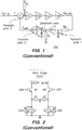
- FIG. 3 shows a circuit 300 for offset cancellation of a continuous-time circuit in accordance with an embodiment of the invention.
- four equalizer stages (Eq1, Eq2, Eq3, and Eq4) are cascaded in a serial chain.
- Other embodiments may have a different number of stages and/or may have cascaded amplifier (rather than equalizer) stages.
- the first equalizer stage (Eq1) receives an input current which is equal to an offset input current (I OFF_IN ).
- I OFF_IN an offset input current
- the correction voltage (V CORR ) output by gm1 in combination with the feedback load represented by C F and R F ) is sent directly to the first stage (without the need for gm2).
- the first parasitic pole (Parasitic pole 1) is due to the low-pass filter, represented by resistor R IN and capacitor C IN , at the input of gm1.
- the second parasitic pole (Parasitic pole A) is due to the first equalizer stage (Eq1) and, as discussed below, may be neglected for phase margin analysis.
- Eq1 the first equalizer stage
- FIG. 4 depicts a circuit implementation of a first equalizer stage (Eq 1 in FIG. 3 ) showing the application of the offset cancellation loop voltage in accordance with an embodiment of the invention. As described below, this control voltage may be used to cancel the offset of the cascaded equalizer chain.
- the first equalizer stage may include a pair of differential transistors (M1 and M2), a pair of offset input transistors (MIsp and MIsn), a pair of offset compensation transistors (Mofcp and Mofcn).
- the stage also includes impedances (Z1 and Z2), with a virtual ground therebetween), resistors (Rfxp and Rfxn), and current sources (I1, I2, Isp and Isn).
- M1 and M2 may be NMOS transistors with gate width/length of Win/Lin
- Mlsp and MIsn may be PMOS transistors with gate width/length W1/L1
- Mofcp and Mofcn may be NMOS transistors with gate width/length W2/L2.
- the differential offset voltage inputs (VOFP and VOFN) are buffered by source follower circuits (comprising current source Isp and transistor MIsp, and current source Isn and transistor Mlsn, respectively).
- the buffered differential voltage inputs (vsfp and vsfn) are applied to the gates of the offset compensation transistors (Mofcp and Mofcn, respectively) which are operating in the "linear" region.
- a differential voltage is developed by the feedback loop as VOFP rises and VOFN falls (and vice-versa) in response to a DC (direct current) offset in the chain.
- the bleed resistors (Rfxp and Rfxn) allow some of the current to bypass Mofcp and Mofcn.
- the amplitude of the correctable offset voltage is determined, in part, by the ratio of resistance between Rfxp and Mofcp (and between Rfxn and Mofcn).
- the amplitude of the correctable offset voltage increases if more of the current is modulated by Mofcp and Mofcn.
- Mofcp and Mofcn also act as additional source degeneration resistors that degrade the effective gain of the input pair (M1 and M2) and so reduces the bandwidth and gain of the stage, i.e. decreases the AC (alternating current) performance of the stage.
- Rfxp and Rfxn are removed (i.e. set to infinity or open circuit), then all the current flows through, and is modulated by, Mofcp and Mofcn. In that case, the maximum achievable correctable offset voltage is reached, but the AC performance of the equalization stage is at a minimum.
- the maximum achievable correctable offset voltage is determined, at least in part, by the product of the tail current (i.e. I 1 and I 2 ) and the range of the variable channel resistance of offset compensation transistor (i.e. the channel resistance of Mofcp and Mofcn).
- Rfxp and Rfxn are set to zero (i.e.
- the differential offset voltages VOFP and VOFN effectively modulate the offset compensation voltages vocn and vocp, where vocn is the voltage at the source of M1, and vocp is the voltage at the source of M2.
- These offset compensation voltages vocn and vocp cause corresponding voltage changes in the differential voltage outputs (OUTP and OUTN), and these differential voltage outputs are provided as the differential voltage inputs of the next stage (Eq2).
- Non-dominant pole A is created by the source follower circuits. (This is the same Non-dominant pole A as in FIG. 3 .)
- Non-dominant pole A is at a frequency of approximately 5 to 6 GHz with minimal power consumption (about 100 microamperes).
- the frequency of Non-dominant pole A is substantially higher (by orders of magnitude) than the frequencies of the parasitic poles shown in FIG. 1 . As such, Non-dominant pole A may be neglected for phase margin analysis.
- the NMOS transistors Mofcp and Mofcn may be maintained in the linear region by sizing them appropriately and by using the PMOS level shifters (Mlsp and Mlsn configured as source followers).
- the source follower circuits also serve as fail safes.
- the source follower circuits may be configured to ensure that, if the threshold voltages of MIsp and MIsn are high, the gate voltages (vsfp and vsfn) applied to Mofcp and Mofcn will still be sufficient to keep them in the linear region.
- the offset compensation loop has one secondary pole (at the input of the offset compensation loop) of consequence and one dominant pole.
- the overall loop gain of the circuit 300 in FIG. 3 may be about 10 dB less than the overall loop gain of the circuit 100 in FIG. 1
- the circuit 300 of FIG. 3 has greater offset cancellation ability since it uses the whole tail current, which can be large.
- the reduced loop gain of the circuit 300 in FIG. 3 makes it easier to stabilize the loop.
- variations in process, voltage and temperature (PVT) have less detrimental effects on stability.
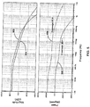
- FIG. 5 is a Bode plot providing a comparison between the conventional offset cancellation loop 100 of FIG. 1 and the offset cancellation loop 300 of FIG. 3 in accordance with an embodiment of the invention.
- the Bode plot shows magnitude (in dB) and phase (in degrees) versus frequency (in Hz) for the conventional and new loops.
- the offset cancellation loop 300 of FIG. 3 was implemented with a similar loop filter size as the conventional offset cancellation loop 100 of FIG. 1 .
- a first Bode magnitude plot 502 shows the loop gain for the conventional offset cancellation loop 100 of FIG. 1
- a second Bode magnitude plot 504 shows the loop gain for the offset cancellation loop 300 of FIG. 3
- a first Bode phase plot 506 shows the frequency-response phase shift of the conventional offset cancellation loop 100 of FIG. 1
- a second Bode phase plot 508 shows the frequency-response phase shift of the conventional offset cancellation loop 300 of FIG. 1 .
- the 0 dB frequency is higher for the conventional offset cancellation loop 100 than for the offset cancellation loop 300 of FIG. 3 .
- the conventional offset cancellation loop 100 of FIG. 1 has a 4 th -order roll-off beyond 100 MHz, while the offset cancellation loop 300 of FIG. 3 has a less-steep 2 nd -order roll-off beyond 300 MHz.
- the phase shift plot begins to bend at much lower frequencies for the conventional offset cancellation loop 100 of FIG. 1 (which begins to bend at around 5 MHz) than for the offset cancellation loop 300 of FIG. 3 (which begins to bend at around 20 MHz).
- the phase margin improvement is about 27 degrees (the difference between the phase margin of about 60 degrees for the loop of FIG. 1 and the phase margin of about 87 degrees for the loop of FIG. 3 ).
- the offset cancellation loop 300 of FIG. 3 is substantially more stable than the conventional offset cancellation loop 100 of FIG. 1 .
- the offset cancellation loop 300 of FIG. 3 can tolerate a substantially greater open loop phase shift (or time delay) before becoming unstable.
- the parasitic poles in the loop 100 of FIG. 1 may make that loop unstable.
- the fewer poles in the loop 300 FIG. 3 also makes loop stability easier to manage for a given filter size.
- the Bode plot of FIG. 5 shows that a phase margin of greater than 80 degrees is achievable with a similar area for the loop filter of FIG. 3 (as compared with the area for the loop filter of FIG. 1 ). However, if a lower phase margin may be tolerated (for example, 60 degrees), then the area for the loop filter of FIG. 3 may be reduced (as compared with the area for the loop filter of FIG. 1 ) while maintaining the same stability.
- FIG. 6 shows the transient response of the offset compensation loop 300 in accordance with an embodiment of the invention.
- the bottom graph shows the output signal 604 which is responsive to the DC offset voltages of the input signal 602.
- the input signal 602 corresponds to the voltage of input signal I OFF_IN
- the output signal 604 corresponds to the voltage signal V OFF_OUT .
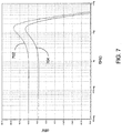
- FIG. 7 shows the forward gain 702 of the conventional offset cancellation loop 100 of FIG. 1 and the forward gain 704 of the offset cancellation loop 300 of FIG. 3 in accordance with an embodiment of the invention.
- the forward gain curve is lower overall for the offset cancellation loop 300 of FIG. 3 .
- a slight degradation in effective gm also causes a lowering in peaking frequency and overall bandwidth.
- the DC gain may need to be increased.
- FIG. 8 shows a circuit 800 for offset cancellation of a continuous-time circuit comprising a circuit of cascaded amplifiers in accordance with an embodiment of the invention.
- This circuit 800 is similar to the circuit 300 in FIG. 3 . The difference is that the chain of equalizer stages (Eq1, Eq2, Eq3, and Eq4) is replaced by a more general chain of amplifier stages (Amp1, Amp2, Amp3, and Amp4).
- the first amplifier stage (Amp1) may be implemented as shown in FIG. 4 .
- FIG. 9 is a simplified partial block diagram of a field programmable gate array (FPGA) 900 that can include aspects of the present invention. It should be understood that embodiments of the present invention can be used in numerous types of integrated circuits such as field programmable gate arrays (FPGAs), programmable logic devices (PLDs), complex programmable logic devices (CPLDs), programmable logic arrays (PLAs), digital signal processors (DSPs) and application specific integrated circuits (ASICs).
- FPGAs field programmable gate arrays
- PLDs programmable logic devices
- CPLDs complex programmable logic devices
- PLAs programmable logic arrays
- DSPs digital signal processors
- ASICs application specific integrated circuits
- FPGA 900 includes within its "core" a two-dimensional array of programmable logic array blocks (or LABs) 902 that are interconnected by a network of column and row interconnect conductors of varying length and speed.
- LABs 902 include multiple (e.g., 10) logic elements (or LEs).
- An LE is a programmable logic block that provides for efficient implementation of user defined logic functions.
- An FPGA has numerous logic elements that can be configured to implement various combinatorial and sequential functions.
- the logic elements have access to a programmable interconnect structure.
- the programmable interconnect structure can be programmed to interconnect the logic elements in almost any desired configuration.
- FPGA 900 may also include a distributed memory structure including random access memory (RAM) blocks of varying sizes provided throughout the array.
- RAM random access memory
- the RAM blocks include, for example, blocks 904, blocks 906, and block 908. These memory blocks can also include shift registers and FIFO buffers.
- FPGA 900 may further include digital signal processing (DSP) blocks 910 that can implement, for example, multipliers with add or subtract features.
- DSP digital signal processing
- IOEs Input/output elements
- Each IOE 912 is coupled to an external terminal (i.e., a pin) of FPGA 900.
- a transceiver (TX/RX) channel array may be arranged as shown, for example, with each TX/RX channel circuit 920 being coupled to several LABs.
- a TX/RX channel circuit 920 may include, among other circuitry, the offset cancellation circuitry described herein.
- FPGA 900 is described herein for illustrative purposes only and that the present invention can be implemented in many different types of PLDs, FPGAs, and ASICs.
- FIG. 10 shows a block diagram of an exemplary digital system 1000 that can embody techniques of the present invention.
- System 1000 may be a programmed digital computer system, digital signal processing system, specialized digital switching network, or other processing system. Moreover, such systems can be designed for a wide variety of applications such as telecommunications systems, automotive systems, control systems, consumer electronics, personal computers, Internet communications and networking, and others. Further, system 1000 may be provided on a single board, on multiple boards, or within multiple enclosures.
- System 1000 includes a processing unit 1002, a memory unit 1004, and an input/output (I/O) unit 1006 interconnected together by one or more buses.
- FPGA 1008 is embedded in processing unit 1002.
- FPGA 1008 can serve many different purposes within the system 1000.
- FPGA 1008 can, for example, be a logical building block of processing unit 1002, supporting its internal and external operations.
- FPGA 1008 is programmed to implement the logical functions necessary to carry on its particular role in system operation.
- FPGA 1008 can be specially coupled to memory 1004 through connection 1010 and to I/O unit 1006 through connection 1012.
- Processing unit 1002 may direct data to an appropriate system component for processing or storage, execute a program stored in memory 1004, receive and transmit data via I/O unit 1006, or other similar function.
- Processing unit 1002 may be a central processing unit (CPU), microprocessor, floating point coprocessor, graphics coprocessor, hardware controller, microcontroller, field programmable gate array programmed for use as a controller, network controller, or any type of processor or controller. Furthermore, in many embodiments, there is often no need for a CPU.
- FPGA 1008 may control the logical operations of the system.
- FPGA 1008 acts as a reconfigurable processor that may be reprogrammed as needed to handle a particular computing task.
- FPGA 1008 may itself include an embedded microprocessor.
- Memory unit 1004 may be a random access memory (RAM), read only memory (ROM), fixed or flexible disk media, flash memory, tape, or any other storage means, or any combination of these storage means.
Claims (13)
- Circuit (300) comprenant :une chaîne d'amplificateur multi-étage (Eq1, Eq2, Eq3, Eq4), comportant un premier étage d'amplificateur (Eq1) et un dernier étage d'amplificateur (Eq4) dans la chaîne ;une boucle d'annulation de décalage configurée pour recevoir une sortie (VOFF_OUT) du dernier étage d'amplificateur (Eq4) et pour fournir un signal de tension de correction de décalage (VCORR, VOFP, VOFN) au premier étage d'amplificateur (Eq1) ;un transistor d'entrée (M1, M2) dans le premier étage d'amplificateur (Eq1), le transistor d'entrée (M1, M2) ayant une grille, une source et un drain, la grille du transistor d'entrée (M1, M2) étant configurée pour recevoir un signal d'entrée (INN, INP) ; etun transistor de compensation de décalage (Mofcp, Mofcn) dans le premier étage d'amplificateur(Eq1), le transistor de compensation de décalage (Mofcp, Mofcn) ayant une grille, une source et un drain, le drain du transistor de compensation de décalage (Mofcp, Mofcn) étant relié électriquement à la source du transistor d'entrée (M1, M2) et une tension sur la grille du transistor de compensation de décalage (Mofcp, Mofcn) étant déterminée par le signal de tension de correction de décalage (VCORR ; VOFN, VOFN) ;caractérise parune impédance (Z1, Z2) qui est reliée électriquement à la source du transistor de compensation de décalage (Mofcp, Mofcn) ; etune source de courant de queue (I1, I2), qui est reliée électriquement à la source du transistor de compensation de décalage (Mofcp, Mofcn) ; etune résistance (Rfxp, Rfxn) configurée en parallèle avec un canal du transistor de compensation de décalage (Mofcp, Mofcn), une extrémité de la résistance étant couplée électriquement à la source du transistor de compensation de décalage (Mofcp, Mofcn), et une autre extrémité de la résistance étant couplée électriquement au drain du transistor de compensation de décalage (Mofcp, Mofcn).
- Circuit (300) de la revendication 1 comprenant en outre :
un circuit suiveur de source (MIsp, Isp ; MIsn, Isn) dans le premier étage d'amplificateur (Eq1), le circuit suiveur de source étant configuré pour recevoir le signal de tension de correction de décalage (VCORR ; VOFN, VOFN) et générer une tension tamponnée qui est appliquée comme la tension (vsfp, vsfn) sur la grille du transistor de compensation de décalage. - Circuit (300) de la revendication 2, dans lequel le circuit suiveur de source comprend une source de courant (Isp, Isn) et un transistor d'entrée du circuit suiveur de source (MIsp, MIsn), dans lequel le signal de tension de correction de décalage (VODFN, VOFN) est appliqué à la grille dudit transistor d'entrée du circuit suiveur de source (MIsp, MIsn), et dans lequel la tension tamponnée est générée à un noeud entre la source de courant et la source d'un transistor d'entrée du circuit suiveur de source (MIsp, MIsn).
- Circuit (300) selon une des revendications 1 à 3, dans lequel la boucle d'annulation de décalage comprend :un seul amplificateur à transconductance (gm1) adapté pour délivrer le signal de tension de correction de décalage (VCORR ; VOFN, VOFN) ;un filtre passe-bas (RIN, CIN) configuré pour recevoir la sortie (VOFF_OUT) du dernier étage d'amplificateur (Eq4) et pour fournir une sortie filtrée à une entrée de l'amplificateur à transconductance (gm1) ; etune charge de rétroaction (RF, CF) couplée à une sortie de l'amplificateur à transconductance (gm1).
- Circuit (300) de la revendication 4, dans lequel la charge de rétroaction comprend une résistance de rétroaction (RF) et un condensateur de rétroaction (CF) qui ont tous deux une extrémité reliée électriquement à la sortie de l'amplificateur à transconductance (gm1) et une autre extrémité reliée électriquement à la terre.
- Circuit (300) selon une des revendications 1 à 5, dans lequel
le signal d'entrée (VOFP, VOFN) est un signal d'entrée différentiel,
le transistor d'entrée (MIsp, MIsn) est un transistor d'une paire de transistors d'entrée configurés pour recevoir le signal d'entrée différentiel (VOFP, VOFN),
le signal de tension de correction de décalage (VCORR ; VOFP, VOFN) est un signal de tension de correction de décalage différentiel, et
le transistor de compensation de décalage (Mofcp, Mofcn) est un transistor d'une paire de transistors de compensation de décalage. - Circuit (300) selon une des revendications 1 à 6, dans lequel la chaîne d'amplificateur multi-étage (Eq1, Eq2, Eq3, Eq4) comprend une chaîne d'égaliseur multi-étage, et les premier et dernier étages d'amplificateur comprennent des premier et dernier étages d'égaliseur, respectivement.
- Circuit (300) selon une des revendications 1 à 7, dans lequel la boucle de compensation de décalage crée un pôle dominant et un seul pôle parasite consécutif, et dans lequel la boucle de compensation de décalage a un affaiblissement du deuxième ordre en amplitude de réponse à des fréquences supérieures.
- Procédé comprenant :la réception d'un signal d'entrée en temps continu (IOFF_IN) par une série d'étages d'amplificateur (Eq1, Eq2, Eq3, Eq4) ;l'amplification du signal d'entrée en temps continu par la série d'étages d'amplificateur (Eq1, Eq2, Eq3, Eq4) de manière à générer un signal de sortie en temps continu (VOFF_OUT) ;l'entrée du signal de sortie en temps continu (VOFF_OUT) dans une boucle d'annulation de décalage ;la génération d'un signal de tension de correction de décalage (VCORR, VOFP, VOFN) par la boucle d'annulation de décalage ; etl'application du signal de tension de correction de décalage (VCORR, VOFP, VOFN) à une grille d'un transistor de compensation de décalage (Mofcp, Mofcn) dans un étage d'amplificateur (Eq1) ;caractérisé parla fourniture d'un courant d'entrée depuis une source de courant de queue (I1, I2), à une source du transistor de compensation de décalage (Mofcp, Mofcn), la source du transistor de compensation de décalage (Mofcp, Mofcn) étant reliée électriquement à la source de courant de queue (I1, I2), une impédance (Z1, Z2) et une résistance (Rfxp, Rfxn) en parallèle avec le canal du transistor de compensation de décalage.
- Procédé de la revendication 9, dans lequel le signal de tension de correction de décalage (Eq1, Eq2, Eq3, Eq4) est généré au moyen d'un seul amplificateur à transconductance (gm1).
- Procédé selon la revendication 9 ou 10, dans lequel la série d'étages d'amplificateur (Eq1, Eq2, Eq3, Eq4) comprend une série d'étages d'égaliseur.
- Procédé selon une des revendications 9 à 11, dans lequel la boucle d'annulation de décalage crée un pôle dominant et un seul pôle secondaire consécutif.
- Procédé selon une des revendications 9 à 12, dans lequel la boucle d'annulation de décalage a un affaiblissement du deuxième ordre en amplitude de réponse à des fréquences supérieures.
Applications Claiming Priority (1)
| Application Number | Priority Date | Filing Date | Title |
|---|---|---|---|
| US12/954,090 US8183921B1 (en) | 2010-11-24 | 2010-11-24 | Offset cancellation for continuous-time circuits |
Publications (3)
| Publication Number | Publication Date |
|---|---|
| EP2458731A2 EP2458731A2 (fr) | 2012-05-30 |
| EP2458731A3 EP2458731A3 (fr) | 2017-04-19 |
| EP2458731B1 true EP2458731B1 (fr) | 2018-08-15 |
Family
ID=45002809
Family Applications (1)
| Application Number | Title | Priority Date | Filing Date |
|---|---|---|---|
| EP11190439.7A Active EP2458731B1 (fr) | 2010-11-24 | 2011-11-24 | Annulation décalée pour circuits en temps continu |
Country Status (3)
| Country | Link |
|---|---|
| US (1) | US8183921B1 (fr) |
| EP (1) | EP2458731B1 (fr) |
| JP (1) | JP6106358B2 (fr) |
Families Citing this family (5)
| Publication number | Priority date | Publication date | Assignee | Title |
|---|---|---|---|---|
| US8456215B2 (en) * | 2011-09-25 | 2013-06-04 | Realtek Semiconductor Corp. | Limiting amplifier and method thereof |
| EP2779438B1 (fr) | 2013-03-15 | 2016-10-26 | Dialog Semiconductor B.V. | Bloqueur CC pour un circuit amplificateur à gain élevé |
| US9917707B2 (en) | 2014-09-11 | 2018-03-13 | The Hong Kong University Of Science And Technology | Adaptive cascaded equalization circuits with configurable roll-up frequency response for spectrum compensation |
| US11444580B2 (en) | 2020-04-01 | 2022-09-13 | Stmicroelectronics International N.V. | Devices and methods for offset cancellation |
| JP2022049988A (ja) | 2020-09-17 | 2022-03-30 | キオクシア株式会社 | 半導体集積回路、受信装置、およびdcオフセットキャンセル方法 |
Family Cites Families (23)
| Publication number | Priority date | Publication date | Assignee | Title |
|---|---|---|---|---|
| US3733558A (en) * | 1971-05-20 | 1973-05-15 | Motorola Inc | Stable low current amplifier |
| US4973919A (en) | 1989-03-23 | 1990-11-27 | Doble Engineering Company | Amplifying with directly coupled, cascaded amplifiers |
| JPH03293806A (ja) * | 1990-04-11 | 1991-12-25 | Fujitsu Ltd | 出力オフセット補償回路 |
| JPH08223228A (ja) * | 1994-03-17 | 1996-08-30 | Fujitsu Ltd | 等化増幅器及びこれを用いた受信機並びにプリアンプ |
| JP2834000B2 (ja) * | 1994-06-29 | 1998-12-09 | 日本電気株式会社 | 中間周波増幅回路 |
| JPH08279718A (ja) * | 1995-04-07 | 1996-10-22 | Nec Corp | オフセット除去増幅回路 |
| JP2809150B2 (ja) * | 1995-08-14 | 1998-10-08 | 日本電気株式会社 | 高利得増幅回路 |
| JP2001223546A (ja) * | 2000-02-08 | 2001-08-17 | Mitsubishi Electric Corp | 多段信号増幅回路 |
| JP2003283266A (ja) * | 2002-03-26 | 2003-10-03 | Toshiba Corp | オフセットキャンセラー回路 |
| US7132882B2 (en) * | 2002-07-19 | 2006-11-07 | Avago Technologies Fiber Ip (Singapore) Pte. Ltd. | Amplifier having multiple offset-compensation paths and related systems and methods |
| US6914479B1 (en) * | 2002-07-26 | 2005-07-05 | International Business Machines Corporation | Differential amplifier with DC offset cancellation |
| US6831510B2 (en) * | 2003-02-06 | 2004-12-14 | Fujitsu Limited | Continuous low-frequency error cancellation in a high-speed differential amplifier |
| US7154335B2 (en) * | 2004-09-29 | 2006-12-26 | Intel Corporation | Variable gain amplifier with direct current offset correction |
| TWI290422B (en) * | 2005-06-09 | 2007-11-21 | Via Tech Inc | Circuit for DC offset cancellation |
| US7321259B1 (en) | 2005-10-06 | 2008-01-22 | Altera Corporation | Programmable logic enabled dynamic offset cancellation |
| US7541857B1 (en) | 2005-12-29 | 2009-06-02 | Altera Corporation | Comparator offset cancellation assisted by PLD resources |
| US7368968B1 (en) | 2005-12-29 | 2008-05-06 | Altera Corporation | Signal offset cancellation |
| US7804892B1 (en) | 2006-02-03 | 2010-09-28 | Altera Corporation | Circuitry for providing programmable decision feedback equalization |
| US7586983B1 (en) | 2006-06-22 | 2009-09-08 | Altera Corporation | Systems and methods for offset cancellation in integrated transceivers |
| US7636003B2 (en) * | 2006-07-21 | 2009-12-22 | Mediatek Inc. | Limiting amplifiers |
| JP4412507B2 (ja) * | 2007-10-03 | 2010-02-10 | Necエレクトロニクス株式会社 | 半導体回路 |
| FI121447B (fi) | 2007-12-28 | 2010-11-15 | Esa Tiiliharju | Kaskadiin kytkettyjen vahvistimien takaisinkytkentäverkko |
| US8654898B2 (en) | 2008-05-08 | 2014-02-18 | Altera Corporation | Digital equalizer for high-speed serial communications |
-
2010
- 2010-11-24 US US12/954,090 patent/US8183921B1/en active Active
-
2011
- 2011-11-22 JP JP2011255026A patent/JP6106358B2/ja not_active Expired - Fee Related
- 2011-11-24 EP EP11190439.7A patent/EP2458731B1/fr active Active
Non-Patent Citations (1)
| Title |
|---|
| None * |
Also Published As
| Publication number | Publication date |
|---|---|
| CN102480271A (zh) | 2012-05-30 |
| JP6106358B2 (ja) | 2017-03-29 |
| US20120126896A1 (en) | 2012-05-24 |
| EP2458731A2 (fr) | 2012-05-30 |
| US8183921B1 (en) | 2012-05-22 |
| JP2012114914A (ja) | 2012-06-14 |
| EP2458731A3 (fr) | 2017-04-19 |
Similar Documents
| Publication | Publication Date | Title |
|---|---|---|
| EP2878079B1 (fr) | Récepteur à large plage d'entrée de mode commun | |
| EP1760885B1 (fr) | Cellule à retard intégrée complètement différentielle en CMOS (C3MOS) contrôlée en courant avec un retard variable | |
| US10033412B2 (en) | Impedance and swing control for voltage-mode driver | |
| US9654310B1 (en) | Analog delay cell and tapped delay line comprising the analog delay cell | |
| US9094244B2 (en) | Receiver circuit with de-emphasis function | |
| US7777526B2 (en) | Increased sensitivity and reduced offset variation in high data rate HSSI receiver | |
| US7009452B2 (en) | Method and apparatus for increasing the linearity and bandwidth of an amplifier | |
| US8810319B1 (en) | Dual-stage continuous-time linear equalizer | |
| EP2458731B1 (fr) | Annulation décalée pour circuits en temps continu | |
| US20170099163A1 (en) | On-Chip AC Coupled Receiver with Real-Time Linear Baseline-Wander Compensation | |
| US9059874B2 (en) | Switched continuous time linear equalizer with integrated sampler | |
| US6570931B1 (en) | Switched voltage adaptive slew rate control and spectrum shaping transmitter for high speed digital transmission | |
| Joo et al. | A data-pattern-tolerant adaptive equalizer using the spectrum balancing method | |
| US10797802B2 (en) | Optical receiver | |
| EP3913800A1 (fr) | Circuit d'égalisation linéaire à temps continu et à large bande passante | |
| WO2021035173A1 (fr) | Commande en mode commun pour récepteurs couplés en courant alternatif | |
| US7302461B2 (en) | Analog delay elements | |
| EP2733897B1 (fr) | Appareil et procédés d'égalisation de retard de récepteur adaptatif | |
| CN114762300A (zh) | 用于串行有线接收器的无源线性均衡器 | |
| US20060088086A1 (en) | Reverse scaling for improved bandwidth in equalizers | |
| KR20230127932A (ko) | 아날로그 전단 회로 및 시스템 | |
| CN110781114B (zh) | 一种高速串行接口接收端的宽带无源线性均衡器电路 | |
| CN110995187A (zh) | 一种应用于高速串行接口的低压宽带线性均衡器电路 | |
| Lu et al. | An adaptive 3.125 Gbps coaxial cable equalizer | |
| Ng et al. | Two-tap travelling-wave infinite impulse response filter with 12 dB peaking at 24 GHz |
Legal Events
| Date | Code | Title | Description |
|---|---|---|---|
| PUAI | Public reference made under article 153(3) epc to a published international application that has entered the european phase |
Free format text: ORIGINAL CODE: 0009012 |
|
| AK | Designated contracting states |
Kind code of ref document: A2 Designated state(s): AL AT BE BG CH CY CZ DE DK EE ES FI FR GB GR HR HU IE IS IT LI LT LU LV MC MK MT NL NO PL PT RO RS SE SI SK SM TR |
|
| AX | Request for extension of the european patent |
Extension state: BA ME |
|
| RIC1 | Information provided on ipc code assigned before grant |
Ipc: H03F 3/45 20060101ALI20161202BHEP Ipc: H03F 1/30 20060101AFI20161202BHEP |
|
| PUAL | Search report despatched |
Free format text: ORIGINAL CODE: 0009013 |
|
| AK | Designated contracting states |
Kind code of ref document: A3 Designated state(s): AL AT BE BG CH CY CZ DE DK EE ES FI FR GB GR HR HU IE IS IT LI LT LU LV MC MK MT NL NO PL PT RO RS SE SI SK SM TR |
|
| AX | Request for extension of the european patent |
Extension state: BA ME |
|
| RIC1 | Information provided on ipc code assigned before grant |
Ipc: H03F 1/30 20060101AFI20170316BHEP Ipc: H03F 3/45 20060101ALI20170316BHEP |
|
| 17P | Request for examination filed |
Effective date: 20171018 |
|
| RBV | Designated contracting states (corrected) |
Designated state(s): AL AT BE BG CH CY CZ DE DK EE ES FI FR GB GR HR HU IE IS IT LI LT LU LV MC MK MT NL NO PL PT RO RS SE SI SK SM TR |
|
| GRAP | Despatch of communication of intention to grant a patent |
Free format text: ORIGINAL CODE: EPIDOSNIGR1 |
|
| INTG | Intention to grant announced |
Effective date: 20180326 |
|
| GRAS | Grant fee paid |
Free format text: ORIGINAL CODE: EPIDOSNIGR3 |
|
| GRAA | (expected) grant |
Free format text: ORIGINAL CODE: 0009210 |
|
| AK | Designated contracting states |
Kind code of ref document: B1 Designated state(s): AL AT BE BG CH CY CZ DE DK EE ES FI FR GB GR HR HU IE IS IT LI LT LU LV MC MK MT NL NO PL PT RO RS SE SI SK SM TR |
|
| REG | Reference to a national code |
Ref country code: CH Ref legal event code: EP Ref country code: GB Ref legal event code: FG4D Ref country code: AT Ref legal event code: REF Ref document number: 1030932 Country of ref document: AT Kind code of ref document: T Effective date: 20180815 |
|
| REG | Reference to a national code |
Ref country code: IE Ref legal event code: FG4D |
|
| REG | Reference to a national code |
Ref country code: DE Ref legal event code: R096 Ref document number: 602011051014 Country of ref document: DE |
|
| REG | Reference to a national code |
Ref country code: FR Ref legal event code: PLFP Year of fee payment: 8 |
|
| REG | Reference to a national code |
Ref country code: NL Ref legal event code: MP Effective date: 20180815 |
|
| REG | Reference to a national code |
Ref country code: LT Ref legal event code: MG4D |
|
| REG | Reference to a national code |
Ref country code: AT Ref legal event code: MK05 Ref document number: 1030932 Country of ref document: AT Kind code of ref document: T Effective date: 20180815 |
|
| PG25 | Lapsed in a contracting state [announced via postgrant information from national office to epo] |
Ref country code: SE Free format text: LAPSE BECAUSE OF FAILURE TO SUBMIT A TRANSLATION OF THE DESCRIPTION OR TO PAY THE FEE WITHIN THE PRESCRIBED TIME-LIMIT Effective date: 20180815 Ref country code: LT Free format text: LAPSE BECAUSE OF FAILURE TO SUBMIT A TRANSLATION OF THE DESCRIPTION OR TO PAY THE FEE WITHIN THE PRESCRIBED TIME-LIMIT Effective date: 20180815 Ref country code: RS Free format text: LAPSE BECAUSE OF FAILURE TO SUBMIT A TRANSLATION OF THE DESCRIPTION OR TO PAY THE FEE WITHIN THE PRESCRIBED TIME-LIMIT Effective date: 20180815 Ref country code: NL Free format text: LAPSE BECAUSE OF FAILURE TO SUBMIT A TRANSLATION OF THE DESCRIPTION OR TO PAY THE FEE WITHIN THE PRESCRIBED TIME-LIMIT Effective date: 20180815 Ref country code: FI Free format text: LAPSE BECAUSE OF FAILURE TO SUBMIT A TRANSLATION OF THE DESCRIPTION OR TO PAY THE FEE WITHIN THE PRESCRIBED TIME-LIMIT Effective date: 20180815 Ref country code: NO Free format text: LAPSE BECAUSE OF FAILURE TO SUBMIT A TRANSLATION OF THE DESCRIPTION OR TO PAY THE FEE WITHIN THE PRESCRIBED TIME-LIMIT Effective date: 20181115 Ref country code: GR Free format text: LAPSE BECAUSE OF FAILURE TO SUBMIT A TRANSLATION OF THE DESCRIPTION OR TO PAY THE FEE WITHIN THE PRESCRIBED TIME-LIMIT Effective date: 20181116 Ref country code: BG Free format text: LAPSE BECAUSE OF FAILURE TO SUBMIT A TRANSLATION OF THE DESCRIPTION OR TO PAY THE FEE WITHIN THE PRESCRIBED TIME-LIMIT Effective date: 20181115 Ref country code: IS Free format text: LAPSE BECAUSE OF FAILURE TO SUBMIT A TRANSLATION OF THE DESCRIPTION OR TO PAY THE FEE WITHIN THE PRESCRIBED TIME-LIMIT Effective date: 20181215 Ref country code: AT Free format text: LAPSE BECAUSE OF FAILURE TO SUBMIT A TRANSLATION OF THE DESCRIPTION OR TO PAY THE FEE WITHIN THE PRESCRIBED TIME-LIMIT Effective date: 20180815 |
|
| PG25 | Lapsed in a contracting state [announced via postgrant information from national office to epo] |
Ref country code: AL Free format text: LAPSE BECAUSE OF FAILURE TO SUBMIT A TRANSLATION OF THE DESCRIPTION OR TO PAY THE FEE WITHIN THE PRESCRIBED TIME-LIMIT Effective date: 20180815 Ref country code: HR Free format text: LAPSE BECAUSE OF FAILURE TO SUBMIT A TRANSLATION OF THE DESCRIPTION OR TO PAY THE FEE WITHIN THE PRESCRIBED TIME-LIMIT Effective date: 20180815 Ref country code: LV Free format text: LAPSE BECAUSE OF FAILURE TO SUBMIT A TRANSLATION OF THE DESCRIPTION OR TO PAY THE FEE WITHIN THE PRESCRIBED TIME-LIMIT Effective date: 20180815 |
|
| PG25 | Lapsed in a contracting state [announced via postgrant information from national office to epo] |
Ref country code: PL Free format text: LAPSE BECAUSE OF FAILURE TO SUBMIT A TRANSLATION OF THE DESCRIPTION OR TO PAY THE FEE WITHIN THE PRESCRIBED TIME-LIMIT Effective date: 20180815 Ref country code: ES Free format text: LAPSE BECAUSE OF FAILURE TO SUBMIT A TRANSLATION OF THE DESCRIPTION OR TO PAY THE FEE WITHIN THE PRESCRIBED TIME-LIMIT Effective date: 20180815 Ref country code: EE Free format text: LAPSE BECAUSE OF FAILURE TO SUBMIT A TRANSLATION OF THE DESCRIPTION OR TO PAY THE FEE WITHIN THE PRESCRIBED TIME-LIMIT Effective date: 20180815 Ref country code: CZ Free format text: LAPSE BECAUSE OF FAILURE TO SUBMIT A TRANSLATION OF THE DESCRIPTION OR TO PAY THE FEE WITHIN THE PRESCRIBED TIME-LIMIT Effective date: 20180815 Ref country code: IT Free format text: LAPSE BECAUSE OF FAILURE TO SUBMIT A TRANSLATION OF THE DESCRIPTION OR TO PAY THE FEE WITHIN THE PRESCRIBED TIME-LIMIT Effective date: 20180815 Ref country code: RO Free format text: LAPSE BECAUSE OF FAILURE TO SUBMIT A TRANSLATION OF THE DESCRIPTION OR TO PAY THE FEE WITHIN THE PRESCRIBED TIME-LIMIT Effective date: 20180815 |
|
| REG | Reference to a national code |
Ref country code: DE Ref legal event code: R097 Ref document number: 602011051014 Country of ref document: DE |
|
| PG25 | Lapsed in a contracting state [announced via postgrant information from national office to epo] |
Ref country code: SM Free format text: LAPSE BECAUSE OF FAILURE TO SUBMIT A TRANSLATION OF THE DESCRIPTION OR TO PAY THE FEE WITHIN THE PRESCRIBED TIME-LIMIT Effective date: 20180815 Ref country code: SK Free format text: LAPSE BECAUSE OF FAILURE TO SUBMIT A TRANSLATION OF THE DESCRIPTION OR TO PAY THE FEE WITHIN THE PRESCRIBED TIME-LIMIT Effective date: 20180815 Ref country code: DK Free format text: LAPSE BECAUSE OF FAILURE TO SUBMIT A TRANSLATION OF THE DESCRIPTION OR TO PAY THE FEE WITHIN THE PRESCRIBED TIME-LIMIT Effective date: 20180815 |
|
| PLBE | No opposition filed within time limit |
Free format text: ORIGINAL CODE: 0009261 |
|
| STAA | Information on the status of an ep patent application or granted ep patent |
Free format text: STATUS: NO OPPOSITION FILED WITHIN TIME LIMIT |
|
| REG | Reference to a national code |
Ref country code: CH Ref legal event code: PL |
|
| 26N | No opposition filed |
Effective date: 20190516 |
|
| PG25 | Lapsed in a contracting state [announced via postgrant information from national office to epo] |
Ref country code: LU Free format text: LAPSE BECAUSE OF NON-PAYMENT OF DUE FEES Effective date: 20181124 Ref country code: MC Free format text: LAPSE BECAUSE OF FAILURE TO SUBMIT A TRANSLATION OF THE DESCRIPTION OR TO PAY THE FEE WITHIN THE PRESCRIBED TIME-LIMIT Effective date: 20180815 |
|
| REG | Reference to a national code |
Ref country code: BE Ref legal event code: MM Effective date: 20181130 |
|
| REG | Reference to a national code |
Ref country code: IE Ref legal event code: MM4A |
|
| PG25 | Lapsed in a contracting state [announced via postgrant information from national office to epo] |
Ref country code: SI Free format text: LAPSE BECAUSE OF FAILURE TO SUBMIT A TRANSLATION OF THE DESCRIPTION OR TO PAY THE FEE WITHIN THE PRESCRIBED TIME-LIMIT Effective date: 20180815 Ref country code: LI Free format text: LAPSE BECAUSE OF NON-PAYMENT OF DUE FEES Effective date: 20181130 Ref country code: CH Free format text: LAPSE BECAUSE OF NON-PAYMENT OF DUE FEES Effective date: 20181130 |
|
| PG25 | Lapsed in a contracting state [announced via postgrant information from national office to epo] |
Ref country code: IE Free format text: LAPSE BECAUSE OF NON-PAYMENT OF DUE FEES Effective date: 20181124 |
|
| PG25 | Lapsed in a contracting state [announced via postgrant information from national office to epo] |
Ref country code: BE Free format text: LAPSE BECAUSE OF NON-PAYMENT OF DUE FEES Effective date: 20181130 |
|
| PG25 | Lapsed in a contracting state [announced via postgrant information from national office to epo] |
Ref country code: MT Free format text: LAPSE BECAUSE OF NON-PAYMENT OF DUE FEES Effective date: 20181124 |
|
| PG25 | Lapsed in a contracting state [announced via postgrant information from national office to epo] |
Ref country code: TR Free format text: LAPSE BECAUSE OF FAILURE TO SUBMIT A TRANSLATION OF THE DESCRIPTION OR TO PAY THE FEE WITHIN THE PRESCRIBED TIME-LIMIT Effective date: 20180815 |
|
| PG25 | Lapsed in a contracting state [announced via postgrant information from national office to epo] |
Ref country code: PT Free format text: LAPSE BECAUSE OF FAILURE TO SUBMIT A TRANSLATION OF THE DESCRIPTION OR TO PAY THE FEE WITHIN THE PRESCRIBED TIME-LIMIT Effective date: 20180815 |
|
| PG25 | Lapsed in a contracting state [announced via postgrant information from national office to epo] |
Ref country code: HU Free format text: LAPSE BECAUSE OF FAILURE TO SUBMIT A TRANSLATION OF THE DESCRIPTION OR TO PAY THE FEE WITHIN THE PRESCRIBED TIME-LIMIT; INVALID AB INITIO Effective date: 20111124 Ref country code: MK Free format text: LAPSE BECAUSE OF NON-PAYMENT OF DUE FEES Effective date: 20180815 Ref country code: CY Free format text: LAPSE BECAUSE OF FAILURE TO SUBMIT A TRANSLATION OF THE DESCRIPTION OR TO PAY THE FEE WITHIN THE PRESCRIBED TIME-LIMIT Effective date: 20180815 |
|
| P01 | Opt-out of the competence of the unified patent court (upc) registered |
Effective date: 20230531 |
|
| PGFP | Annual fee paid to national office [announced via postgrant information from national office to epo] |
Ref country code: GB Payment date: 20230914 Year of fee payment: 13 |
|
| PGFP | Annual fee paid to national office [announced via postgrant information from national office to epo] |
Ref country code: FR Payment date: 20230921 Year of fee payment: 13 |
|
| PGFP | Annual fee paid to national office [announced via postgrant information from national office to epo] |
Ref country code: DE Payment date: 20230919 Year of fee payment: 13 |