EP2453476A1 - Procédé d'emballage de dispositif semi-conducteur et emballage de dispositif semi-conducteur - Google Patents
Procédé d'emballage de dispositif semi-conducteur et emballage de dispositif semi-conducteur Download PDFInfo
- Publication number
- EP2453476A1 EP2453476A1 EP10191081A EP10191081A EP2453476A1 EP 2453476 A1 EP2453476 A1 EP 2453476A1 EP 10191081 A EP10191081 A EP 10191081A EP 10191081 A EP10191081 A EP 10191081A EP 2453476 A1 EP2453476 A1 EP 2453476A1
- Authority
- EP
- European Patent Office
- Prior art keywords
- semiconductor device
- discrete semiconductor
- contact area
- recess
- leadframe
- Prior art date
- Legal status (The legal status is an assumption and is not a legal conclusion. Google has not performed a legal analysis and makes no representation as to the accuracy of the status listed.)
- Withdrawn
Links
- 239000004065 semiconductor Substances 0.000 title claims abstract description 104
- 238000000034 method Methods 0.000 title claims description 25
- 238000004806 packaging method and process Methods 0.000 title description 4
- 239000010410 layer Substances 0.000 claims abstract description 30
- 238000007747 plating Methods 0.000 claims abstract description 24
- 238000004519 manufacturing process Methods 0.000 claims abstract description 7
- 239000011241 protective layer Substances 0.000 claims abstract description 7
- 238000000465 moulding Methods 0.000 claims description 13
- 230000001681 protective effect Effects 0.000 claims description 11
- 238000005530 etching Methods 0.000 claims description 8
- 239000003795 chemical substances by application Substances 0.000 claims description 7
- 239000011888 foil Substances 0.000 claims description 7
- 239000011248 coating agent Substances 0.000 claims description 5
- 238000000576 coating method Methods 0.000 claims description 5
- 239000000853 adhesive Substances 0.000 claims description 4
- 230000001070 adhesive effect Effects 0.000 claims description 4
- 239000012778 molding material Substances 0.000 claims description 3
- 229910000679 solder Inorganic materials 0.000 claims description 3
- 229920005989 resin Polymers 0.000 description 4
- 239000011347 resin Substances 0.000 description 4
- 239000000463 material Substances 0.000 description 3
- 238000013459 approach Methods 0.000 description 2
- 238000005476 soldering Methods 0.000 description 2
- HRANPRDGABOKNQ-ORGXEYTDSA-N (1r,3r,3as,3br,7ar,8as,8bs,8cs,10as)-1-acetyl-5-chloro-3-hydroxy-8b,10a-dimethyl-7-oxo-1,2,3,3a,3b,7,7a,8,8a,8b,8c,9,10,10a-tetradecahydrocyclopenta[a]cyclopropa[g]phenanthren-1-yl acetate Chemical compound C1=C(Cl)C2=CC(=O)[C@@H]3C[C@@H]3[C@]2(C)[C@@H]2[C@@H]1[C@@H]1[C@H](O)C[C@@](C(C)=O)(OC(=O)C)[C@@]1(C)CC2 HRANPRDGABOKNQ-ORGXEYTDSA-N 0.000 description 1
- 229910000577 Silicon-germanium Inorganic materials 0.000 description 1
- ATJFFYVFTNAWJD-UHFFFAOYSA-N Tin Chemical compound [Sn] ATJFFYVFTNAWJD-UHFFFAOYSA-N 0.000 description 1
- 239000012790 adhesive layer Substances 0.000 description 1
- 230000015572 biosynthetic process Effects 0.000 description 1
- 239000003990 capacitor Substances 0.000 description 1
- 150000001875 compounds Chemical class 0.000 description 1
- 238000011109 contamination Methods 0.000 description 1
- 238000005520 cutting process Methods 0.000 description 1
- 230000001419 dependent effect Effects 0.000 description 1
- 238000007772 electroless plating Methods 0.000 description 1
- 229920006336 epoxy molding compound Polymers 0.000 description 1
- 239000004922 lacquer Substances 0.000 description 1
- 238000003698 laser cutting Methods 0.000 description 1
- 239000002184 metal Substances 0.000 description 1
- 229910052751 metal Inorganic materials 0.000 description 1
- 229910001092 metal group alloy Inorganic materials 0.000 description 1
- 150000003071 polychlorinated biphenyls Chemical class 0.000 description 1
- 238000000926 separation method Methods 0.000 description 1
- 229910052710 silicon Inorganic materials 0.000 description 1
- 239000010703 silicon Substances 0.000 description 1
- 229910052709 silver Inorganic materials 0.000 description 1
- 239000004332 silver Substances 0.000 description 1
- -1 tape Substances 0.000 description 1
- 239000010409 thin film Substances 0.000 description 1
- 239000011135 tin Substances 0.000 description 1
- 229910052718 tin Inorganic materials 0.000 description 1
Images


Classifications
-
- H—ELECTRICITY
- H01—ELECTRIC ELEMENTS
- H01L—SEMICONDUCTOR DEVICES NOT COVERED BY CLASS H10
- H01L23/00—Details of semiconductor or other solid state devices
- H01L23/48—Arrangements for conducting electric current to or from the solid state body in operation, e.g. leads, terminal arrangements ; Selection of materials therefor
- H01L23/488—Arrangements for conducting electric current to or from the solid state body in operation, e.g. leads, terminal arrangements ; Selection of materials therefor consisting of soldered or bonded constructions
- H01L23/495—Lead-frames or other flat leads
- H01L23/49541—Geometry of the lead-frame
- H01L23/49562—Geometry of the lead-frame for devices being provided for in H01L29/00
-
- H—ELECTRICITY
- H01—ELECTRIC ELEMENTS
- H01L—SEMICONDUCTOR DEVICES NOT COVERED BY CLASS H10
- H01L23/00—Details of semiconductor or other solid state devices
- H01L23/48—Arrangements for conducting electric current to or from the solid state body in operation, e.g. leads, terminal arrangements ; Selection of materials therefor
- H01L23/488—Arrangements for conducting electric current to or from the solid state body in operation, e.g. leads, terminal arrangements ; Selection of materials therefor consisting of soldered or bonded constructions
- H01L23/495—Lead-frames or other flat leads
- H01L23/49541—Geometry of the lead-frame
- H01L23/49548—Cross section geometry
-
- H—ELECTRICITY
- H01—ELECTRIC ELEMENTS
- H01L—SEMICONDUCTOR DEVICES NOT COVERED BY CLASS H10
- H01L24/00—Arrangements for connecting or disconnecting semiconductor or solid-state bodies; Methods or apparatus related thereto
- H01L24/93—Batch processes
- H01L24/95—Batch processes at chip-level, i.e. with connecting carried out on a plurality of singulated devices, i.e. on diced chips
- H01L24/97—Batch processes at chip-level, i.e. with connecting carried out on a plurality of singulated devices, i.e. on diced chips the devices being connected to a common substrate, e.g. interposer, said common substrate being separable into individual assemblies after connecting
-
- H—ELECTRICITY
- H01—ELECTRIC ELEMENTS
- H01L—SEMICONDUCTOR DEVICES NOT COVERED BY CLASS H10
- H01L2224/00—Indexing scheme for arrangements for connecting or disconnecting semiconductor or solid-state bodies and methods related thereto as covered by H01L24/00
- H01L2224/01—Means for bonding being attached to, or being formed on, the surface to be connected, e.g. chip-to-package, die-attach, "first-level" interconnects; Manufacturing methods related thereto
- H01L2224/26—Layer connectors, e.g. plate connectors, solder or adhesive layers; Manufacturing methods related thereto
- H01L2224/28—Structure, shape, material or disposition of the layer connectors prior to the connecting process
- H01L2224/29—Structure, shape, material or disposition of the layer connectors prior to the connecting process of an individual layer connector
- H01L2224/29001—Core members of the layer connector
- H01L2224/29099—Material
- H01L2224/29198—Material with a principal constituent of the material being a combination of two or more materials in the form of a matrix with a filler, i.e. being a hybrid material, e.g. segmented structures, foams
- H01L2224/29199—Material of the matrix
- H01L2224/2929—Material of the matrix with a principal constituent of the material being a polymer, e.g. polyester, phenolic based polymer, epoxy
-
- H—ELECTRICITY
- H01—ELECTRIC ELEMENTS
- H01L—SEMICONDUCTOR DEVICES NOT COVERED BY CLASS H10
- H01L2224/00—Indexing scheme for arrangements for connecting or disconnecting semiconductor or solid-state bodies and methods related thereto as covered by H01L24/00
- H01L2224/01—Means for bonding being attached to, or being formed on, the surface to be connected, e.g. chip-to-package, die-attach, "first-level" interconnects; Manufacturing methods related thereto
- H01L2224/26—Layer connectors, e.g. plate connectors, solder or adhesive layers; Manufacturing methods related thereto
- H01L2224/28—Structure, shape, material or disposition of the layer connectors prior to the connecting process
- H01L2224/29—Structure, shape, material or disposition of the layer connectors prior to the connecting process of an individual layer connector
- H01L2224/29001—Core members of the layer connector
- H01L2224/29099—Material
- H01L2224/29198—Material with a principal constituent of the material being a combination of two or more materials in the form of a matrix with a filler, i.e. being a hybrid material, e.g. segmented structures, foams
- H01L2224/29298—Fillers
- H01L2224/29299—Base material
- H01L2224/293—Base material with a principal constituent of the material being a metal or a metalloid, e.g. boron [B], silicon [Si], germanium [Ge], arsenic [As], antimony [Sb], tellurium [Te] and polonium [Po], and alloys thereof
-
- H—ELECTRICITY
- H01—ELECTRIC ELEMENTS
- H01L—SEMICONDUCTOR DEVICES NOT COVERED BY CLASS H10
- H01L2224/00—Indexing scheme for arrangements for connecting or disconnecting semiconductor or solid-state bodies and methods related thereto as covered by H01L24/00
- H01L2224/01—Means for bonding being attached to, or being formed on, the surface to be connected, e.g. chip-to-package, die-attach, "first-level" interconnects; Manufacturing methods related thereto
- H01L2224/26—Layer connectors, e.g. plate connectors, solder or adhesive layers; Manufacturing methods related thereto
- H01L2224/31—Structure, shape, material or disposition of the layer connectors after the connecting process
- H01L2224/32—Structure, shape, material or disposition of the layer connectors after the connecting process of an individual layer connector
- H01L2224/321—Disposition
- H01L2224/32151—Disposition the layer connector connecting between a semiconductor or solid-state body and an item not being a semiconductor or solid-state body, e.g. chip-to-substrate, chip-to-passive
- H01L2224/32221—Disposition the layer connector connecting between a semiconductor or solid-state body and an item not being a semiconductor or solid-state body, e.g. chip-to-substrate, chip-to-passive the body and the item being stacked
- H01L2224/32245—Disposition the layer connector connecting between a semiconductor or solid-state body and an item not being a semiconductor or solid-state body, e.g. chip-to-substrate, chip-to-passive the body and the item being stacked the item being metallic
-
- H—ELECTRICITY
- H01—ELECTRIC ELEMENTS
- H01L—SEMICONDUCTOR DEVICES NOT COVERED BY CLASS H10
- H01L2224/00—Indexing scheme for arrangements for connecting or disconnecting semiconductor or solid-state bodies and methods related thereto as covered by H01L24/00
- H01L2224/80—Methods for connecting semiconductor or other solid state bodies using means for bonding being attached to, or being formed on, the surface to be connected
- H01L2224/83—Methods for connecting semiconductor or other solid state bodies using means for bonding being attached to, or being formed on, the surface to be connected using a layer connector
- H01L2224/83001—Methods for connecting semiconductor or other solid state bodies using means for bonding being attached to, or being formed on, the surface to be connected using a layer connector involving a temporary auxiliary member not forming part of the bonding apparatus
- H01L2224/83005—Methods for connecting semiconductor or other solid state bodies using means for bonding being attached to, or being formed on, the surface to be connected using a layer connector involving a temporary auxiliary member not forming part of the bonding apparatus being a temporary or sacrificial substrate
-
- H—ELECTRICITY
- H01—ELECTRIC ELEMENTS
- H01L—SEMICONDUCTOR DEVICES NOT COVERED BY CLASS H10
- H01L2224/00—Indexing scheme for arrangements for connecting or disconnecting semiconductor or solid-state bodies and methods related thereto as covered by H01L24/00
- H01L2224/93—Batch processes
- H01L2224/95—Batch processes at chip-level, i.e. with connecting carried out on a plurality of singulated devices, i.e. on diced chips
- H01L2224/97—Batch processes at chip-level, i.e. with connecting carried out on a plurality of singulated devices, i.e. on diced chips the devices being connected to a common substrate, e.g. interposer, said common substrate being separable into individual assemblies after connecting
-
- H—ELECTRICITY
- H01—ELECTRIC ELEMENTS
- H01L—SEMICONDUCTOR DEVICES NOT COVERED BY CLASS H10
- H01L2924/00—Indexing scheme for arrangements or methods for connecting or disconnecting semiconductor or solid-state bodies as covered by H01L24/00
- H01L2924/0001—Technical content checked by a classifier
- H01L2924/00011—Not relevant to the scope of the group, the symbol of which is combined with the symbol of this group
-
- H—ELECTRICITY
- H01—ELECTRIC ELEMENTS
- H01L—SEMICONDUCTOR DEVICES NOT COVERED BY CLASS H10
- H01L2924/00—Indexing scheme for arrangements or methods for connecting or disconnecting semiconductor or solid-state bodies as covered by H01L24/00
- H01L2924/10—Details of semiconductor or other solid state devices to be connected
- H01L2924/11—Device type
- H01L2924/12—Passive devices, e.g. 2 terminal devices
- H01L2924/1204—Optical Diode
- H01L2924/12042—LASER
-
- H—ELECTRICITY
- H01—ELECTRIC ELEMENTS
- H01L—SEMICONDUCTOR DEVICES NOT COVERED BY CLASS H10
- H01L2924/00—Indexing scheme for arrangements or methods for connecting or disconnecting semiconductor or solid-state bodies as covered by H01L24/00
- H01L2924/15—Details of package parts other than the semiconductor or other solid state devices to be connected
- H01L2924/181—Encapsulation
Definitions
- the present invention relates to a method of packaging a discrete semiconductor device such as a diode.
- the present invention further relates to a discrete semiconductor device obtained by such a method.
- Discrete semiconductor devices such as diodes are typically provided in a package when marketed.
- the package protects the discrete semiconductor device from accidental damage and provides the contacts for integrating the discrete semiconductor device in a larger electronic device, e.g. by mounting the discrete semiconductor device on a printer circuit board (PCB).
- PCB printer circuit board
- the package contacts are typically fan-outs of the contacts of the discrete semiconductor device, i.e. have a larger area, as manufacturing approaches to reproduce the small dimensions of a discrete semiconductor device at the package level in a straightforward and cost-effective manner are currently unavailable.
- the present invention seeks to provide a method of manufacturing a discrete semiconductor device package that facilitates the manufacture of packages smaller than 0603 packages.
- the present invention further seeks to provide a discrete semiconductor device package obtained by such a method.
- a method of manufacturing a discrete semiconductor device package comprising providing a leadframe; forming a recess in said leadframe, said recess having a depth substantially equal to the thickness of the discrete semiconductor device, wherein a raised portion of the leadframe adjacent to said recess defines a first contact area; placing the discrete semiconductor device with its active side face down in said recess, wherein the exposed surface of the discrete semiconductor device defines a second contact area; molding the resultant product in a protective layer, leaving the surface including the first contact area and the second contact area exposed; and covering the exposed first contact area and the second contact area with respective plating layers.
- a very compact package can be manufactured having reduced dimensions. This is further facilitated by the partial molding of the package and the provision of a solderable plating layer on the exposed contact areas, such that these contact areas can be used to attach the package to a suitable carrier without requiring fan-out of the contact areas, thus further reducing the form factor of the package.
- the recess may be formed by stamping or etching, if necessary combined with a flattening step to ensure that the recess has the appropriate depth.
- the discrete semiconductor device has its active side placed face down, i.e. facing the recess surface. This facilitates extending a contact between the second contact area and a carrier over the side of the discrete semiconductor package, which would not be possible in case the active side would be facing upwards, as such an arrangement would likely result in an electrical short in case of the contact extending over the side of the package.
- the step of placing the discrete semiconductor device in said recess comprises interconnecting the placing the discrete semiconductor device to the leadframe using a conductive fixating agent.
- the conductive fixating agent may for instance be a conductive adhesive paste or conductive wafer back coating.
- Such a fixation technique can be realized using a very thin layer of the fixating agent, thus further aiding in limiting the overall dimensions of the package.
- said placing step comprises placing the discrete semiconductor device in said recess with its active side down.
- the step of etching said recess comprises etching a plurality of recesses in said leadframe, wherein raised portions of the leadframe adjacent to each of said recesses define respective first contact areas; and the step of placing the discrete semiconductor device in said recess comprises placing a discrete semiconductor device in each of said recesses, the exposed surfaces of the discrete semiconductor devices defining respective second contact areas; the method further comprising separating the leadframe into individualized discrete semiconductor device packages.
- a plurality of packages may be formed from a single leadframe.
- the difference between the thickness of the discrete semiconductor device and the depth of the recess is less than 0.1 mm. This ensures that the first and second contact areas can be effectively mounted onto a flat surface.
- the molding step may be used to negate any difference between the depth of the recess and the thickness of the discrete semiconductor device.
- the step of molding the resultant product in a protective layer comprises covering the first contact area and the second contact area with a protective foil. This ensures that the contact areas do not become contaminated with molding material.
- the backside of the leadframe i.e. the side that received the active side of the discrete semiconductor device is protected from being covered by the molding material, for instance by a standard lead frame tape.
- a discrete semiconductor device package comprising a leadframe portion comprising a recess having a depth substantially equal to the thickness of the discrete semiconductor device, wherein a raised portion of the leadframe adjacent to said recess defines a first contact area; a discrete semiconductor device in said recess, wherein the exposed surface of the discrete semiconductor device defines a second contact area; a protective layer covering the leadframe portion and the discrete semiconductor device but not the first contact area and the second contact area; and respective plating layers covering the first contact area and the second contact area.
- Such a package can be manufactured to smaller dimensions than what is currently possible, thus aiding the further miniaturization of such packages.
- the surface opposite the surface including the first contact and the second contact is covered with a protective, electrically insulating layer.
- the electrically insulating layer may be formed using a lacquer, tape, foil, and so on.
- the respective plating layers each cap a respective end surface of the package. This has the advantage that a solder interconnecting the contact areas to respective carrier contacts may extend vertically onto these plating caps, thereby improving the quality of the contact between the discrete semiconductor device package and the carrier.
- a carrier comprising a first carrier contact and a second carrier contact, said carrier further comprising the discrete semiconductor device package according to an embodiment of the present invention, wherein the first carrier contact is conductively connected to the first contact area and the second carrier contact is conductively connected to the second contact area by respective solder portions.
- a carrier may for instance be an electronic device, a printed circuit board, a multi-chip module, and so on.
- a suitable leadframe 10 e.g. a leadless carrier such as a QFN (quad flat no leads) or a MCD leadframe
- a recess 14 is provided e.g. by stamping or etching with any suitable etch recipe to provide a leadframe 10 in which a first contact portion 12 is defined adjacent to the recess 14.
- the recess 14 has a depth that is equal or close to the thickness of the discrete semiconductor device to be placed in the recess 14.
- the desired depth of the recess may for instance be achieved by combination of an etching or stamping step with a subsequent flattening step.
- the difference between the thickness of the discrete semiconductor device and the depth of the recess 14 is less than 0.1 mm.
- the thickness of the discrete semiconductor device is identical to the depth of the recess to the extent that the exposed surface of the discrete semiconductor device lies in the same plane as the surface area of the first contact portion 12.
- FIG. 1 depicts a leadframe 10 comprising a single recess 14 and a single contact portion 12 for the sake of clarity. It should however be understood that in a preferred embodiment the leadframe 10 comprises an array of recesses 14 and adjacent contact portions 12 such that a plurality of packages may be formed from a single leadframe 10.
- the discrete semiconductor device 20 is placed in the recess 14. This is shown in FIG. 2 .
- the discrete semiconductor device 20 has a contact surface 22 defining a second contact area.
- the contact surface 22 preferably lies in the same plane as the surface of the first contact portion 12.
- the discrete semiconductor device 20 may be conductively interconnected to the leadframe 10 in any suitable manner.
- the conductive interconnection may be formed using conductive adhesive paste or wafer back coating. If the discrete semiconductor device 20 is placed onto the leadframe 10 with its active side down, this implies that the wafer back coating is applied to the top side of the wafer of the discrete semiconductor device 20.
- the discrete semiconductor device 20 may be any suitable semiconductor device.
- the discrete semiconductor device 20 may be a discrete diode, although other discrete devices, e.g. transistors, are equally feasible.
- the wafer material from which the discrete semiconductor device 20 is formed may be any suitable semiconductor material, such as silicon, SiGe and so on.
- the active area of the discrete semiconductor device 20 including seal ring is kept smaller than 0.2 mm, such that the total package width can be limited to 0.2 mm.
- the resultant structure is molded with a protective resin, which envelopes the leadframe 10 and the discrete semiconductor device 20 placed thereon.
- a protective resin which envelopes the leadframe 10 and the discrete semiconductor device 20 placed thereon.
- the first contact surface 12 and the second contact surface 22 are left exposed. This may be achieved in any suitable manner, for instance by covering these contact surfaces with a foil to protect them from being covered by the protective resin.
- the foil may simply be removed to expose the first contact surface 12 and the second contact surface 22.
- Any suitable protective resin such as an epoxy molding compound may be used.
- a protective, electrically insulating layer 32 is applied to the back side of the leadframe, as shown in FIG. 3 .
- the first contact surface 12 and the discrete semiconductor device 20 are connected via the leadframe 10, the first contact surface 12 and the second contact surface 22 are only connected by the function in the IC, e.g. a diode function and the remainder of the IC needs to be insulated from the first contact surface 12, which is the purpose of the electrically insulating layer 32.
- the leadframe 10 may be separated into the individualized discrete semiconductor packages in any suitable manner, e.g. by dicing, cutting or sawing. This is not explicitly shown.
- the contact surfaces 12 and 22 of the separate discrete semiconductor packages are provided with a solderable plating 40 as shown in FIG. 4 to yield the finalized separate discrete semiconductor device package 100.
- the plating 40 may be applied in any suitable manner, e.g. barrel plating, or alternatively electroless plating may be used.
- the second contact surface 22 of the discrete semiconductor device 20 is only partially covered by the plating layer 40 by way of non-limiting example only. It should be understood that it is equally feasible to cover the whole contact surface 22 with the plating layer 40. This will be typically determined by the size of the discrete semiconductor device 20.
- FIG. 5 shows the placement of the dies 20 onto a leadframe 10 having raised contact portions 12 as previously explained.
- the leadframe 10 may comprise a leadframe tape 31 to electrically insulate the bottom of the leadframe.
- the resultant structure may be molded with a protective resin 30, such that the first contact surfaces 12 and the second contact surfaces 22 remain exposed.
- the molding step is a foil-assisted molding step in which the first contact surfaces 12 and the second contact surfaces 22 are protected by a foil (not shown) during molding to avoid contamination of these contact surfaces.
- the lead frame tape 31 may be removed and replaced with an electrically insulating layer 32 as shown in FIG. 3 such as a tape marketed by the Lintec Corporation, Japan to electrically insulate the bottom of the leadframe.
- the leadframe 10 may be separated in strips 34 as shown in FIG. 7 . This may be done in any suitable manner, e.g. dicing, sawing, laser cutting and so on.
- the strips 34 are subsequently stacked as schematically shown in FIG. 8 (it should be understood that the strips 34 are shown separated from each other for clarity purposes; in reality they are stacked in physical contact with each other) , after which a seed layer 36 is sputtered onto the surfaces to be plated as shown in FIG. 9 .
- Any suitable metal may be used for such a seed layer.
- the surfaces to receive the seed layer may be treated with e.g. a plasma etch to increase the adhesion of the seed layer to the surfaces.
- the process proceeds as shown in FIG. 10 with a contact plating step to form side contacts 40, after which the strips are separated into individual discrete semiconductor device packages 100 as shown in FIG. 11 .
- the contact plating step may also cover the first contact area 12 and the second contact area 22, as for instance is shown in FIG. 10 .
- the process may continue from FIG. 6 as shown in FIG. 12 , in which the leadframe 10 and mounted dies 20 are separated into individual components 50 that are subsequently placed in a frame 60, as shown in FIG. 13 .
- the frame 60 may be supported by a support tape 70 to improve the fixation of the individual components 50.
- a conductive paste is applied to the surfaces of the individual components 50 to be plated followed by a contact plating step to finalize the discrete semiconductor device packages 100. Both sides of the components 50 may be plated in this manner.
- plating processes are for instance well-known from the production of passive components such as multi-layer chip capacitors and thin film resistors.
- Suitable plating materials include tin, silver, metal alloys and layer stacks such as a niAu finish, NiPdAu and so on.
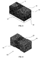
- FIG. 4 depicts a preferred embodiment of the discrete semiconductor device package 100, in which the plating layers 40 cap the end portions of the package. This will be explained in more detail with the aid of FIG. 14 . However, it should be understood that it is not essential for the plating layers 40 to completely cover the end portions of the package 100. Alternative embodiments, such as an embodiment in which the plating layers 40 only cover the respective surfaces 12 and 22 are equally feasible.
- discrete semiconductor device packages are mounted on a carrier such as a PCB in a top/bottom contact orientation, with the bottom contact directly bonded to the carrier, and with the top contact being a wire bonding contact for wire bonding the top contact to the carrier.
- the provision of the wire bonding contact requires a minimum area which has prohibited the reduction of the package size beyond certain dimensions.
- the replacement of a wire bonding contact with the conductive adhesive layer between the discrete semiconductor device 20 and the leadframe 10 facilitates the sideways mounting of such packages on a carrier 200 such as a PCB as shown in FIG. 14 , with the solderable plating layers 40 providing the contacts from the package 100 to the outside world.
- Carrier 200 has a first contact 210 and a second contact 220, to which the discrete semiconductor device package 100 is soldered using soldering 150.
- the provision of the plating layers 40 as caps on the end portions of the discrete semiconductor device package 100 enables the soldering 150 to extend vertically from the respective contacts 210 and 220.
- the sideways mounting of the discrete semiconductor device package 100 allows the package to be used with PCBs that have been designed to receive larger form factor components, e.g. 0603 diode packages.
Landscapes
- Engineering & Computer Science (AREA)
- Computer Hardware Design (AREA)
- Microelectronics & Electronic Packaging (AREA)
- Power Engineering (AREA)
- Physics & Mathematics (AREA)
- Condensed Matter Physics & Semiconductors (AREA)
- General Physics & Mathematics (AREA)
- Geometry (AREA)
- Lead Frames For Integrated Circuits (AREA)
Priority Applications (3)
| Application Number | Priority Date | Filing Date | Title |
|---|---|---|---|
| EP10191081A EP2453476A1 (fr) | 2010-11-12 | 2010-11-12 | Procédé d'emballage de dispositif semi-conducteur et emballage de dispositif semi-conducteur |
| US13/294,126 US20120286410A1 (en) | 2010-11-12 | 2011-11-10 | Semiconductor device packaging method and semiconductor device package |
| CN2011103584133A CN102468194A (zh) | 2010-11-12 | 2011-11-11 | 半导体器件封装方法及半导体器件封装 |
Applications Claiming Priority (1)
| Application Number | Priority Date | Filing Date | Title |
|---|---|---|---|
| EP10191081A EP2453476A1 (fr) | 2010-11-12 | 2010-11-12 | Procédé d'emballage de dispositif semi-conducteur et emballage de dispositif semi-conducteur |
Publications (1)
| Publication Number | Publication Date |
|---|---|
| EP2453476A1 true EP2453476A1 (fr) | 2012-05-16 |
Family
ID=43902909
Family Applications (1)
| Application Number | Title | Priority Date | Filing Date |
|---|---|---|---|
| EP10191081A Withdrawn EP2453476A1 (fr) | 2010-11-12 | 2010-11-12 | Procédé d'emballage de dispositif semi-conducteur et emballage de dispositif semi-conducteur |
Country Status (3)
| Country | Link |
|---|---|
| US (1) | US20120286410A1 (fr) |
| EP (1) | EP2453476A1 (fr) |
| CN (1) | CN102468194A (fr) |
Cited By (1)
| Publication number | Priority date | Publication date | Assignee | Title |
|---|---|---|---|---|
| US8981566B2 (en) | 2012-06-01 | 2015-03-17 | Nxp B.V. | Discrete semiconductor device package and manufacturing method |
Families Citing this family (5)
| Publication number | Priority date | Publication date | Assignee | Title |
|---|---|---|---|---|
| TWI501363B (zh) * | 2014-01-10 | 2015-09-21 | Sfi Electronics Technology Inc | 一種小型化表面黏著型二極體封裝元件及其製法 |
| TWI651830B (zh) * | 2015-02-17 | 2019-02-21 | 立昌先進科技股份有限公司 | 多功能小型化表面黏著型電子元件及其製法 |
| CN104637914B (zh) * | 2015-02-28 | 2018-02-13 | 立昌先进科技股份有限公司 | 多功能表面黏着型电子组件及其制法 |
| EP3065172A1 (fr) | 2015-03-06 | 2016-09-07 | Nxp B.V. | Dispositif semi-conducteur |
| US10256168B2 (en) | 2016-06-12 | 2019-04-09 | Nexperia B.V. | Semiconductor device and lead frame therefor |
Citations (5)
| Publication number | Priority date | Publication date | Assignee | Title |
|---|---|---|---|---|
| JP2001203301A (ja) * | 2000-01-21 | 2001-07-27 | Shindengen Electric Mfg Co Ltd | 樹脂封止型半導体装置及びその製造方法 |
| US20040266037A1 (en) * | 2003-06-26 | 2004-12-30 | Semiconductor Components Industries, Llc. | Direct chip attach structure and method |
| DE102005004160A1 (de) * | 2005-01-28 | 2006-08-10 | Infineon Technologies Ag | Halbleiterbaustein und Verfahren zum Herstellen desselben |
| US7166496B1 (en) * | 2005-08-17 | 2007-01-23 | Ciclon Semiconductor Device Corp. | Method of making a packaged semiconductor device |
| US20100127365A1 (en) * | 2008-11-24 | 2010-05-27 | Manolito Galera | Leadframe-based chip scale semiconductor packages |
Family Cites Families (9)
| Publication number | Priority date | Publication date | Assignee | Title |
|---|---|---|---|---|
| US5814884C1 (en) * | 1996-10-24 | 2002-01-29 | Int Rectifier Corp | Commonly housed diverse semiconductor die |
| US6133634A (en) * | 1998-08-05 | 2000-10-17 | Fairchild Semiconductor Corporation | High performance flip chip package |
| US6262489B1 (en) * | 1999-11-08 | 2001-07-17 | Delphi Technologies, Inc. | Flip chip with backside electrical contact and assembly and method therefor |
| JP3943395B2 (ja) * | 2000-03-22 | 2007-07-11 | インターナショナル・レクチファイヤー・コーポレーション | ゲートドライバマルチチップモジュール |
| US6624522B2 (en) * | 2000-04-04 | 2003-09-23 | International Rectifier Corporation | Chip scale surface mounted device and process of manufacture |
| US20050029666A1 (en) * | 2001-08-31 | 2005-02-10 | Yasutoshi Kurihara | Semiconductor device structural body and electronic device |
| US6891256B2 (en) * | 2001-10-22 | 2005-05-10 | Fairchild Semiconductor Corporation | Thin, thermally enhanced flip chip in a leaded molded package |
| US6946740B2 (en) * | 2002-07-15 | 2005-09-20 | International Rectifier Corporation | High power MCM package |
| EP2669936B1 (fr) * | 2012-06-01 | 2018-02-14 | Nexperia B.V. | Ensemble de dispositif semi-conducteur discret et procédé de fabrication |
-
2010
- 2010-11-12 EP EP10191081A patent/EP2453476A1/fr not_active Withdrawn
-
2011
- 2011-11-10 US US13/294,126 patent/US20120286410A1/en not_active Abandoned
- 2011-11-11 CN CN2011103584133A patent/CN102468194A/zh active Pending
Patent Citations (5)
| Publication number | Priority date | Publication date | Assignee | Title |
|---|---|---|---|---|
| JP2001203301A (ja) * | 2000-01-21 | 2001-07-27 | Shindengen Electric Mfg Co Ltd | 樹脂封止型半導体装置及びその製造方法 |
| US20040266037A1 (en) * | 2003-06-26 | 2004-12-30 | Semiconductor Components Industries, Llc. | Direct chip attach structure and method |
| DE102005004160A1 (de) * | 2005-01-28 | 2006-08-10 | Infineon Technologies Ag | Halbleiterbaustein und Verfahren zum Herstellen desselben |
| US7166496B1 (en) * | 2005-08-17 | 2007-01-23 | Ciclon Semiconductor Device Corp. | Method of making a packaged semiconductor device |
| US20100127365A1 (en) * | 2008-11-24 | 2010-05-27 | Manolito Galera | Leadframe-based chip scale semiconductor packages |
Cited By (2)
| Publication number | Priority date | Publication date | Assignee | Title |
|---|---|---|---|---|
| US8981566B2 (en) | 2012-06-01 | 2015-03-17 | Nxp B.V. | Discrete semiconductor device package and manufacturing method |
| US9263335B2 (en) | 2012-06-01 | 2016-02-16 | Nxp B.V. | Discrete semiconductor device package and manufacturing method |
Also Published As
| Publication number | Publication date |
|---|---|
| CN102468194A (zh) | 2012-05-23 |
| US20120286410A1 (en) | 2012-11-15 |
Similar Documents
| Publication | Publication Date | Title |
|---|---|---|
| US11842948B2 (en) | SMDs integration on QFN by 3D stacked solution | |
| CN103681607A (zh) | 半导体器件及其制作方法 | |
| KR20020012901A (ko) | 이식성 도전패턴을 포함하는 반도체 패키지 및 그 제조방법 | |
| US20090026594A1 (en) | Thin Plastic Leadless Package with Exposed Metal Die Paddle | |
| US7944031B2 (en) | Leadframe-based chip scale semiconductor packages | |
| US20120286410A1 (en) | Semiconductor device packaging method and semiconductor device package | |
| US20210035891A1 (en) | Semiconductor packages and methods of packaging semiconductor devices | |
| US9263335B2 (en) | Discrete semiconductor device package and manufacturing method | |
| JP2005294443A (ja) | 半導体装置及びその製造方法 | |
| US10529680B2 (en) | Encapsulated electronic device mounted on a redistribution layer | |
| US6339253B1 (en) | Semiconductor package | |
| CN108074901B (zh) | 具有可湿拐角引线的半导体器件及半导体器件组装方法 | |
| US20120025357A1 (en) | Leadframe for ic package and method of manufacture | |
| US7960211B2 (en) | Semiconductor system-in-package and method for making the same | |
| KR100817030B1 (ko) | 반도체 패키지 및 이의 제조방법 | |
| CN116097400A (zh) | 具有堆叠无源部件的多层半导体封装件 | |
| US9947632B2 (en) | Semiconductor device and method of making a semiconductor device | |
| US20220320033A1 (en) | Semiconductor Device and Method of Disposing Electrical Components Above and Below Substrate | |
| US10361146B2 (en) | Semiconductor package with multiple stacked leadframes and a method of manufacturing the same | |
| US20170018487A1 (en) | Thermal enhancement for quad flat no lead (qfn) packages | |
| US9142496B1 (en) | Semiconductor package having etched foil capacitor integrated into leadframe | |
| JP2021100053A (ja) | 半導体装置及びその製造方法 | |
| KR20050038502A (ko) | 적층 칩 패키지 제조 방법 | |
| JP2010283158A (ja) | 半導体装置およびその製造方法 |
Legal Events
| Date | Code | Title | Description |
|---|---|---|---|
| PUAI | Public reference made under article 153(3) epc to a published international application that has entered the european phase |
Free format text: ORIGINAL CODE: 0009012 |
|
| AK | Designated contracting states |
Kind code of ref document: A1 Designated state(s): AL AT BE BG CH CY CZ DE DK EE ES FI FR GB GR HR HU IE IS IT LI LT LU LV MC MK MT NL NO PL PT RO RS SE SI SK SM TR |
|
| AX | Request for extension of the european patent |
Extension state: BA ME |
|
| 17P | Request for examination filed |
Effective date: 20121116 |
|
| 17Q | First examination report despatched |
Effective date: 20130411 |
|
| STAA | Information on the status of an ep patent application or granted ep patent |
Free format text: STATUS: THE APPLICATION IS DEEMED TO BE WITHDRAWN |
|
| 18D | Application deemed to be withdrawn |
Effective date: 20130824 |