EP2434557B1 - Photoelectric conversion element, solid-state imaging element, imaging apparatus, and method for manufacturing photoelectric conversion element - Google Patents
Photoelectric conversion element, solid-state imaging element, imaging apparatus, and method for manufacturing photoelectric conversion element Download PDFInfo
- Publication number
- EP2434557B1 EP2434557B1 EP11182753.1A EP11182753A EP2434557B1 EP 2434557 B1 EP2434557 B1 EP 2434557B1 EP 11182753 A EP11182753 A EP 11182753A EP 2434557 B1 EP2434557 B1 EP 2434557B1
- Authority
- EP
- European Patent Office
- Prior art keywords
- electrode
- group
- amount
- light receiving
- photoelectric conversion
- Prior art date
- Legal status (The legal status is an assumption and is not a legal conclusion. Google has not performed a legal analysis and makes no representation as to the accuracy of the status listed.)
- Active
Links
Images

Classifications
-
- H—ELECTRICITY
- H10—SEMICONDUCTOR DEVICES; ELECTRIC SOLID-STATE DEVICES NOT OTHERWISE PROVIDED FOR
- H10F—INORGANIC SEMICONDUCTOR DEVICES SENSITIVE TO INFRARED RADIATION, LIGHT, ELECTROMAGNETIC RADIATION OF SHORTER WAVELENGTH OR CORPUSCULAR RADIATION
- H10F30/00—Individual radiation-sensitive semiconductor devices in which radiation controls the flow of current through the devices, e.g. photodetectors
- H10F30/20—Individual radiation-sensitive semiconductor devices in which radiation controls the flow of current through the devices, e.g. photodetectors the devices having potential barriers, e.g. phototransistors
-
- H—ELECTRICITY
- H01—ELECTRIC ELEMENTS
- H01L—SEMICONDUCTOR DEVICES NOT COVERED BY CLASS H10
- H01L21/00—Processes or apparatus adapted for the manufacture or treatment of semiconductor or solid state devices or of parts thereof
- H01L21/02—Manufacture or treatment of semiconductor devices or of parts thereof
- H01L21/02104—Forming layers
- H01L21/02365—Forming inorganic semiconducting materials on a substrate
- H01L21/02518—Deposited layers
- H01L21/02521—Materials
- H01L21/02565—Oxide semiconducting materials not being Group 12/16 materials, e.g. ternary compounds
-
- C—CHEMISTRY; METALLURGY
- C23—COATING METALLIC MATERIAL; COATING MATERIAL WITH METALLIC MATERIAL; CHEMICAL SURFACE TREATMENT; DIFFUSION TREATMENT OF METALLIC MATERIAL; COATING BY VACUUM EVAPORATION, BY SPUTTERING, BY ION IMPLANTATION OR BY CHEMICAL VAPOUR DEPOSITION, IN GENERAL; INHIBITING CORROSION OF METALLIC MATERIAL OR INCRUSTATION IN GENERAL
- C23C—COATING METALLIC MATERIAL; COATING MATERIAL WITH METALLIC MATERIAL; SURFACE TREATMENT OF METALLIC MATERIAL BY DIFFUSION INTO THE SURFACE, BY CHEMICAL CONVERSION OR SUBSTITUTION; COATING BY VACUUM EVAPORATION, BY SPUTTERING, BY ION IMPLANTATION OR BY CHEMICAL VAPOUR DEPOSITION, IN GENERAL
- C23C14/00—Coating by vacuum evaporation, by sputtering or by ion implantation of the coating forming material
- C23C14/06—Coating by vacuum evaporation, by sputtering or by ion implantation of the coating forming material characterised by the coating material
- C23C14/0676—Oxynitrides
-
- C—CHEMISTRY; METALLURGY
- C23—COATING METALLIC MATERIAL; COATING MATERIAL WITH METALLIC MATERIAL; CHEMICAL SURFACE TREATMENT; DIFFUSION TREATMENT OF METALLIC MATERIAL; COATING BY VACUUM EVAPORATION, BY SPUTTERING, BY ION IMPLANTATION OR BY CHEMICAL VAPOUR DEPOSITION, IN GENERAL; INHIBITING CORROSION OF METALLIC MATERIAL OR INCRUSTATION IN GENERAL
- C23C—COATING METALLIC MATERIAL; COATING MATERIAL WITH METALLIC MATERIAL; SURFACE TREATMENT OF METALLIC MATERIAL BY DIFFUSION INTO THE SURFACE, BY CHEMICAL CONVERSION OR SUBSTITUTION; COATING BY VACUUM EVAPORATION, BY SPUTTERING, BY ION IMPLANTATION OR BY CHEMICAL VAPOUR DEPOSITION, IN GENERAL
- C23C16/00—Chemical coating by decomposition of gaseous compounds, without leaving reaction products of surface material in the coating, i.e. chemical vapour deposition [CVD] processes
- C23C16/22—Chemical coating by decomposition of gaseous compounds, without leaving reaction products of surface material in the coating, i.e. chemical vapour deposition [CVD] processes characterised by the deposition of inorganic material, other than metallic material
- C23C16/30—Deposition of compounds, mixtures or solid solutions, e.g. borides, carbides, nitrides
- C23C16/308—Oxynitrides
-
- H—ELECTRICITY
- H10—SEMICONDUCTOR DEVICES; ELECTRIC SOLID-STATE DEVICES NOT OTHERWISE PROVIDED FOR
- H10F—INORGANIC SEMICONDUCTOR DEVICES SENSITIVE TO INFRARED RADIATION, LIGHT, ELECTROMAGNETIC RADIATION OF SHORTER WAVELENGTH OR CORPUSCULAR RADIATION
- H10F39/00—Integrated devices, or assemblies of multiple devices, comprising at least one element covered by group H10F30/00, e.g. radiation detectors comprising photodiode arrays
- H10F39/10—Integrated devices
- H10F39/12—Image sensors
-
- H—ELECTRICITY
- H10—SEMICONDUCTOR DEVICES; ELECTRIC SOLID-STATE DEVICES NOT OTHERWISE PROVIDED FOR
- H10K—ORGANIC ELECTRIC SOLID-STATE DEVICES
- H10K30/00—Organic devices sensitive to infrared radiation, light, electromagnetic radiation of shorter wavelength or corpuscular radiation
- H10K30/80—Constructional details
- H10K30/81—Electrodes
- H10K30/82—Transparent electrodes, e.g. indium tin oxide [ITO] electrodes
-
- H—ELECTRICITY
- H10—SEMICONDUCTOR DEVICES; ELECTRIC SOLID-STATE DEVICES NOT OTHERWISE PROVIDED FOR
- H10K—ORGANIC ELECTRIC SOLID-STATE DEVICES
- H10K39/00—Integrated devices, or assemblies of multiple devices, comprising at least one organic radiation-sensitive element covered by group H10K30/00
- H10K39/10—Organic photovoltaic [PV] modules; Arrays of single organic PV cells
-
- H—ELECTRICITY
- H10—SEMICONDUCTOR DEVICES; ELECTRIC SOLID-STATE DEVICES NOT OTHERWISE PROVIDED FOR
- H10K—ORGANIC ELECTRIC SOLID-STATE DEVICES
- H10K39/00—Integrated devices, or assemblies of multiple devices, comprising at least one organic radiation-sensitive element covered by group H10K30/00
- H10K39/30—Devices controlled by radiation
- H10K39/32—Organic image sensors
-
- H—ELECTRICITY
- H10—SEMICONDUCTOR DEVICES; ELECTRIC SOLID-STATE DEVICES NOT OTHERWISE PROVIDED FOR
- H10K—ORGANIC ELECTRIC SOLID-STATE DEVICES
- H10K30/00—Organic devices sensitive to infrared radiation, light, electromagnetic radiation of shorter wavelength or corpuscular radiation
- H10K30/10—Organic devices sensitive to infrared radiation, light, electromagnetic radiation of shorter wavelength or corpuscular radiation comprising heterojunctions between organic semiconductors and inorganic semiconductors
- H10K30/15—Sensitised wide-bandgap semiconductor devices, e.g. dye-sensitised TiO2
- H10K30/151—Sensitised wide-bandgap semiconductor devices, e.g. dye-sensitised TiO2 the wide bandgap semiconductor comprising titanium oxide, e.g. TiO2
-
- Y—GENERAL TAGGING OF NEW TECHNOLOGICAL DEVELOPMENTS; GENERAL TAGGING OF CROSS-SECTIONAL TECHNOLOGIES SPANNING OVER SEVERAL SECTIONS OF THE IPC; TECHNICAL SUBJECTS COVERED BY FORMER USPC CROSS-REFERENCE ART COLLECTIONS [XRACs] AND DIGESTS
- Y02—TECHNOLOGIES OR APPLICATIONS FOR MITIGATION OR ADAPTATION AGAINST CLIMATE CHANGE
- Y02E—REDUCTION OF GREENHOUSE GAS [GHG] EMISSIONS, RELATED TO ENERGY GENERATION, TRANSMISSION OR DISTRIBUTION
- Y02E10/00—Energy generation through renewable energy sources
- Y02E10/50—Photovoltaic [PV] energy
- Y02E10/549—Organic PV cells
-
- Y—GENERAL TAGGING OF NEW TECHNOLOGICAL DEVELOPMENTS; GENERAL TAGGING OF CROSS-SECTIONAL TECHNOLOGIES SPANNING OVER SEVERAL SECTIONS OF THE IPC; TECHNICAL SUBJECTS COVERED BY FORMER USPC CROSS-REFERENCE ART COLLECTIONS [XRACs] AND DIGESTS
- Y02—TECHNOLOGIES OR APPLICATIONS FOR MITIGATION OR ADAPTATION AGAINST CLIMATE CHANGE
- Y02P—CLIMATE CHANGE MITIGATION TECHNOLOGIES IN THE PRODUCTION OR PROCESSING OF GOODS
- Y02P70/00—Climate change mitigation technologies in the production process for final industrial or consumer products
- Y02P70/50—Manufacturing or production processes characterised by the final manufactured product
Definitions
- the present invention relates to an electrode structure for a photoelectric conversion element, an imaging apparatus, and a method for manufacturing a photoelectric conversion element.
- JP-A-2001-007367 describes a manufacturing method in which pixel electrodes are formed and then heated at 230 °C or higher.
- this patent document does not describe a specific configuration for enhancing the heat resistance.
- the invention has been made, and an object thereof is to provide an electrode structure for a photoelectric conversion element, the photoelectric conversion element including an organic material-containing light receiving layer, which is able to enhance heat resistance regardless of the material of the light receiving layer. Also, another object of the invention is to provide a method for manufacturing this photoelectric conversion element, a method for manufacturing a solid-state imaging element equipped with this photoelectric conversion element, and an imaging apparatus equipped with a solid-state imaging element, which has been obtained by the respective method.
- a composition of the first electrode just before forming the light receiving layer further meets (3) a requirement that an amount of nitrogen contained in the whole of the first electrodes is 50 at% to 73 at% of an amount of titanium, or (4) a requirement that in a range of from the substrate side of the first electrode to 10 nm or a range of from the substrate side of the first electrode to 2/3 of the thickness of the first electrode, an amount of nitrogen is 50 at% to 90 at% of an amount of titanium.
- Subject-matter of the present invention is an electrode structure as claimed in claim 1, a method for manufacturing a photoelectric conversion element as claimed in claim 2, a method for manufacturing a solid-state imaging element as claimed in claim 5, and an imaging apparatus as claimed in claim 6.
- Embodiments of the method of claim 2 are claimed in dependent claims 3 and 4.
- a photoelectric conversion element in which an insulating film constituted of an oxide film is formed on a substrate and which includes pixel electrodes formed on the insulating film, an organic material-containing light receiving layer formed on the pixel electrodes and a counter electrode formed on the light receiving layer, the present inventors made investigation on how to enhance the heat resistance. As a result, it has been found that in the case where each of the pixel electrodes is constituted of titanium oxynitride (TiON), even when the same light receiving layer is used, the heat resistance of the photoelectric conversion element is different depending upon a ratio of at least one of oxygen and nitrogen to titanium in the pixel electrode.
- TiON titanium oxynitride
- a composition of the pixel electrode just before forming the light receiving layer meets (1) a requirement that an amount of oxygen contained in the whole of pixel electrodes is 75 at% or more (preferably 85 at% or more, and more preferably 100 at% or more) of an amount of titanium, or (2) a requirement that in a range of from the substrate side of the pixel electrode to 10 nm or a range of from the substrate side of the pixel electrode to 2/3 of the whole thickness, an amount of oxygen is 40 at% or more (preferably 60 at% or more, and more preferably 70 at% or more) of an amount of titanium, the heat resistance of the light receiving layer to be formed thereon is enhanced.
- an oxygen ratio within the pixel electrode is excessively high, electric conductivity is lowered, and hence, it is preferable that the amount of oxygen is 150 at% or less relative to the amount of titanium in all of the requirements (1) and (2).
- a composition of the pixel electrode just before forming the light receiving layer meets (3) a requirement that an amount of nitrogen contained in the whole of pixel electrodes is 73 at% or less (preferably 65 at% or less, and more preferably 50 at% or less) of an amount of titanium, or (4) a requirement that in a range of from the substrate side of the pixel electrode to 10 nm or a range of from the substrate side of the pixel electrode to 2/3 of the whole thickness, an amount of nitrogen is 90 at% or less (preferably 80 at% or less, and more preferably 50 at% or less) of an amount of titanium, the heat resistance of the light receiving layer to be formed thereon is enhanced.
- a requirement (1) or (2), and further a requirement (3) or (4) are met.
- the amount of nitrogen is 50 at% to 73 at% of an amount of titanium, and according to requirement (4) of the present invention, the amount of nitrogen is 50 at% to 90 at% of an amount of titanium.
- the heating step to be performed later on the photoelectric conversion element means a high-temperature heating treatment which is performed in, for example, curing of a color filter, wire bonding, die bonding, solder reflow, formation of a PAD opening, or the like (in general, a heating treatment at 200 °C or higher), which are performed after the formation of a counter electrode.
- oxygen is incorporated into the pixel electrodes from an oxide film (for example, an SiO2 film) existing beneath the pixel electrodes, and as a result, for example, a very small amount of a gas spouts to act on the light receiving layer, thereby possibly producing a process of deteriorating the performance.
- oxide film for example, an SiO2 film
- a volatilized gas is not certain, in view of the facts that deterioration of the performance of the light receiving layer is inhibited by controlling an amount of nitrogen in the pixel electrodes to a fixed amount or less; and that a ratio of nitrogen to titanium decreases after heating the pixel electrodes as compared with that before heating, it may be assumed that a nitrogen-containing gas volatilizes. For that reason, it may be considered that it is preferable to control the amount of nitrogen in the pixel electrodes to a fixed amount or less. In consequence, it may be considered that it is effective to meet the foregoing requirement (3), i.e. an amount of nitrogen contained in the whole of the first electrode is 50 at% to 73 at% of an amount of titanium.
- volatilization of a nitrogen-containing gas component following at the time of the heating step to be performed later on the photoelectric conversion element is caused due to incorporation of oxygen from the oxide film on the substrate surface.
- the ratio of nitrogen is small in not only the whole of pixel electrodes but the neighborhood of the substrate surface.
- volatilization of a nitrogen-containing gas component following at the time of the heating step to be performed later on the photoelectric conversion element is caused due to incorporation of oxygen from the oxide film on the substrate surface. For that reason, in order that a large quantity of oxygen may not penetrate into the pixel electrodes after the heating step, it may be considered to be effective that a composition of the pixel electrode just before forming the light receiving layer meets the foregoing requirement (1).
- both the foregoing requirement (1) or (2) and the foregoing requirement (3) or (4) are met, because it may be considered that the incorporation of oxygen and the volatilization of a gas is effectively prevented from occurring.
- an oxide film for example, silicon oxide
- a substrate such as silicon and glass
- titanium oxynitride is film-formed thereon by means of sputtering; and this titanium oxynitride is subjected to patterning by means of photolithography and etching, thereby forming plural pixel electrodes.
- the plural pixel electrodes are heated, and thereafter, a light receiving layer and a counter electrode are successively formed on the plural pixel electrodes, thereby accomplishing a photoelectric conversion element.
- a temperature in heating the plural pixel electrodes is 270 °C or higher.
- the temperature in heating the plural pixel electrodes is preferably not higher than 800 °C.
- the substrate 101 is a glass substrate or a semiconductor substrate made of silicon or the like.
- the insulating layer 102 made of silicon oxide is formed on the substrate 101.
- a plurality of the pixel electrodes 104 are arranged and formed on the surface of the insulating layer 102, and the connection electrodes 103 are formed corresponding to the pixel electrodes 104 within the insulating layer 102.
- the counter electrode 108 is an electrode counter to to the pixel electrodes 104 and is provided on the light receiving layer 107 to cover the light receiving layer 107.
- the counter electrode 108 is formed extending over the connection electrodes 103 disposed outside the light receiving layer 107 and electrically connected to the connection electrodes 103.
- the counter electrode 108 is preferably constituted of a transparent electrically conductive film, and examples of a material constituting the counter electrode 108 include metals, metal oxides, metal nitrides, metal borides, organic electrically conductive compounds, and mixtures thereof.
- electrically conductive metal oxides such as tin oxide, zinc oxide, indium oxide, indium tin oxide (ITO), indium zinc oxide (IZO), indium tungsten oxide (IWO), and titanium oxide; metal nitrides such as TiN; metals such as gold (Au), platinum (Pt), silver (Ag), chromium (Cr), nickel (Ni), and aluminum (Al); mixtures or stacks of such metal and electrically conductive metal oxide; organic electrically conductive compounds such as polyaniline, polythiophene, and polypyrrole; and stacks of such an organic electrically conductive compound and ITO.
- electrically conductive metal oxides such as tin oxide, zinc oxide, indium oxide, indium tin oxide (ITO), indium zinc oxide (IZO), indium tungsten oxide (IWO), and titanium oxide
- metal nitrides such as TiN
- metals such as gold (Au), platinum (Pt), silver (Ag), chromium (Cr), nickel
- any one of materials of ITO, IZO, tin oxide, antimony-doped tin oxide (ATO), fluorine-doped tin oxide (FTO), zinc oxide, antimony-doped zinc oxide (AZO), and gallium-doped zinc oxide (GZO) is especially preferable as the material of the transparent electrically conductive film.
- connection part 106 is embedded in the insulating layer 102 and is a plug for electrically connecting the connection electrode 103 and the counter electrode voltage supply part 115 to each other, or the like.
- the counter electrode voltage supply part 115 is formed in the substrate 101 and impresses a prescribed voltage to the counter electrode 108 via the connection part 106 and the connection electrode 103.
- the foregoing prescribed voltage is supplied by boosting the power supply voltage by a charge pump boosting circuit or the like.
- the pixel electrode 104 is a charge collecting electrode for collecting a charge generated within the light receiving layer 107 existing between the pixel electrode 104 and the counter electrode 108 counter to the pixel electrode 104.
- the pixel electrode 104 is constituted of titanium oxynitride (TiON).
- TiON titanium oxynitride
- the read-out circuit 116 is configured of, for example, CCD, an MOS circuit, a TFT circuit, or the like and shielded from light by a non-illustrated light shielding layer disposed within the insulting layer 102.
- the buffer layer 109 is formed on the counter electrode 108 to cover the counter electrode 108.
- the sealing layer 110 is formed on the buffer layer 109 to cover the butter layer 109.
- the color filter 111 is formed on the sealing layer 110 at a position counter to each of the pixel electrodes 104.
- the partition wall 112 is provided between the color filters 111 each other and is one for enhancing light transmission efficiency of the color filter 111.
- the light shielding layer 113 is formed on the sealing layer 110 in other regions than those in which the color filters 111 and the partition walls 112 are provided and prevents light from incidence into the light receiving layer 107 formed in other region than the effective pixel region.
- the protective layer 114 is formed on the color filters 111, the partition walls 112 and the light shielding layers 113 and protects the whole of the solid-state imaging element 100.
- connection electrode 103 a plural number of a set of the connection electrode 103, the connection part 106 and the counter electrode voltage supply part 115 is provided. However, only one set may also be provided. As seen in the example of Fig. 1 , by supplying a voltage to the counter electrode 108 from the both ends of the counter electrode 108, a voltage drop in the counter electrode 108 can be inhibited. The number of this set may be properly increased or decreased taking into consideration a chip area of the element.
- a preferred configuration of the light receiving layer 107 is hereunder described.
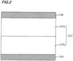
- Fig. 2 is a section showing an example of the configuration of the light receiving layer 107.
- the light receiving layer 107 includes a charge blocking layer 107b provided on the side of the pixel electrode 104 and a photoelectric conversion layer 107a provided on the charge blocking layer 107b.
- a positional relation between the charge blocking layer 107b and the photoelectric conversion layer 107a may be reversed.
- the charge blocking layer 107b has a function to inhibit a dark current.
- the charge blocking layer may be configured of plural layers. By configuring the charge blocking layer 107b of plural layers, an interface between the plural charge blocking layers is formed, and discontinuity is generated in an intermediate level existing in each of the layers, whereby a charge carrier hardly transfers via the intermediate level, and a dark current can be strongly inhibited.
- the photoelectric conversion layer 107a includes a p-type organic semiconductor and an n-type organic semiconductor. By joining the p-type organic semiconductor and the n-type organic semiconductor to form a donor/acceptor interface, exciton dissociation efficiency can be increased. For that reason, the photoelectric conversion layer 107a having a configuration in which the p-type organic semiconductor and the n-type organic semiconductor are joined reveals high photoelectric conversion efficiency. In particular, the photoelectric conversion layer 107a in which the p-type organic semiconductor and the n-type organic semiconductor are mixed is preferable because a joined interface increases, whereby the photoelectric conversion efficiency is enhanced.
- the p-type organic semiconductor is an organic semiconductor with donor properties and means an organic compound which is represented chiefly by hole transporting organic compounds and which has properties of easily donating an electron.
- the p-type organic semiconductor refers to an organic compound having a smaller ionization potential when two organic materials are brought into contact with each other.
- any organic compound can be used so far as it is an organic compound having electron donating properties.
- Examples of the compound which can be used include triarylamine compounds, benzidine compounds, pyrazoline compounds, styrylamine compounds, hydrazone compounds, triphenylmethane compounds, carbazole compounds, polysilane compounds, thiophene compounds, phthalocyanine compounds, cyanine compounds, merocyanine compounds, oxonol compounds, polyamine compounds, indole compounds, pyrrole compounds, pyrazole compounds, polyarylene compounds, condensed aromatic carbocyclic compounds (for example, naphthalene derivatives, anthracene derivatives, phenanthrene derivatives, tetracene derivatives, pyrene derivatives, perylene derivatives, fluoranthene derivatives, etc.), and metal complexes having a nitrogen-containing heterocyclic compound as a ligand.
- the compound is not limited to those described above, and an organic compound may be used as the organic semiconductor with donor properties so far as it has an ionization potential smaller than
- the n-type organic semiconductor is an organic semiconductor with acceptor properties and means an organic compound which is represented chiefly by electron transporting organic compounds and which has properties of easily accepting an electron.
- the n-type organic semiconductor refers to an organic compound having a larger electron affinity when two organic materials are brought into contact with each other.
- any organic compound can be used so far as it is an organic compound having electron accepting properties.
- Examples of the compound which can be used include condensed aromatic carbocyclic compounds (for example, naphthalene derivatives, anthracene derivatives, phenanthrene derivatives, tetracene derivatives, pyrene derivatives, perylene derivatives, fluoranthene derivatives, etc.), 5-membered to 7-membered heterocyclic compounds containing a nitrogen atom, an oxygen atom or a sulfur atom (for example, pyridine, pyrazine, pyrimidine, pyridazine, triazine, quinoline, quinoxaline, quinazoline, phthalazine, cinnoline, isoquinoline, pteridine, acridine, phenazine, phenanthroline, tetrazole, pyrazole, imidazole, thiazole, oxazole, indazole, benzimidazole, benzotriazole, benzoxazole, benzothi
- any organic dye may be used. Preferred examples thereof include cyanine dyes, styryl dyes, hemicyanine dyes, merocyanine dyes (including zero-methine merocyanine (simple merocyanine)), trinuclear merocyanine dyes, tetranuclear merocyanine dyes, rhodacyanine dyes, complex cyanine dyes, complex merocyanine dyes, allopolar dyes, oxonol dyes, hemioxonol dyes, squarium dyes, croconium dyes, azamethine dyes, coumarin dyes, allylidene dyes, anthraquinone dyes, triphenylmethane dyes, azo dyes, azomethine dyes, spiro compounds, metallocene dyes, fluorenone dyes, fulgide dye
- a fullerene or a fullerene derivative having excellent electron transport properties.
- the fullerene as referred to herein expresses fullerene C60, fullerene C70, fullerene C76, fullerene C78, fullerene C80, fullerene C82, fullerene C84, fullerene C90, fullerene C96, fullerene C240, fullerene C540, a mixed fullerene, or a fullerene nanotube; and the fullerene derivative as referred to herein expresses a compound in which a substituent is added such a fullerene.
- an electron donating organic material can be used.
- a low molecular weight material which can be used include aromatic diamine compounds such as N,N'-bis(3-methylphenyl)-(1,1'-biphenyl)-4,4'-diamine (TPD) and 4,4'-bis[N-(naphthyl)-N-phenyl-amino]biphenyl ( ⁇ -NPD), oxazole, oxadiazole, triazole, imidazole, imidazolone, stilbene derivatives, pyrazoline derivatives, tetrahydroimidazole, polyarylalkanes, butadiene, 4,4',4"-tris(N-(3-methylphenyl)N-phenylamino)triphenylamine (m-MTDATA), porphyrin compounds such as porphine, tetraphenylporphine copper, phthalocyanine, copper
- the disclosed photoelectric conversion element is one in which the light receiving layer includes an organic material-containing charge blocking layer and an organic material-containing photoelectric conversion layer.
Landscapes
- Chemical & Material Sciences (AREA)
- Engineering & Computer Science (AREA)
- Physics & Mathematics (AREA)
- Organic Chemistry (AREA)
- General Physics & Mathematics (AREA)
- Chemical Kinetics & Catalysis (AREA)
- Power Engineering (AREA)
- Materials Engineering (AREA)
- Mechanical Engineering (AREA)
- Metallurgy (AREA)
- Electromagnetism (AREA)
- Condensed Matter Physics & Semiconductors (AREA)
- Microelectronics & Electronic Packaging (AREA)
- Manufacturing & Machinery (AREA)
- Computer Hardware Design (AREA)
- General Chemical & Material Sciences (AREA)
- Inorganic Chemistry (AREA)
- Solid State Image Pick-Up Elements (AREA)
- Light Receiving Elements (AREA)
- Electroluminescent Light Sources (AREA)
Applications Claiming Priority (3)
| Application Number | Priority Date | Filing Date | Title |
|---|---|---|---|
| JP2010216102 | 2010-09-27 | ||
| JP2011169650 | 2011-08-02 | ||
| JP2011209209A JP5677921B2 (ja) | 2010-09-27 | 2011-09-26 | 光電変換素子の製造方法 |
Publications (3)
| Publication Number | Publication Date |
|---|---|
| EP2434557A2 EP2434557A2 (en) | 2012-03-28 |
| EP2434557A3 EP2434557A3 (en) | 2018-02-21 |
| EP2434557B1 true EP2434557B1 (en) | 2025-07-02 |
Family
ID=44719488
Family Applications (1)
| Application Number | Title | Priority Date | Filing Date |
|---|---|---|---|
| EP11182753.1A Active EP2434557B1 (en) | 2010-09-27 | 2011-09-26 | Photoelectric conversion element, solid-state imaging element, imaging apparatus, and method for manufacturing photoelectric conversion element |
Country Status (5)
| Country | Link |
|---|---|
| US (1) | US8994132B2 (enExample) |
| EP (1) | EP2434557B1 (enExample) |
| JP (1) | JP5677921B2 (enExample) |
| KR (1) | KR101884021B1 (enExample) |
| CN (1) | CN102420236B (enExample) |
Families Citing this family (14)
| Publication number | Priority date | Publication date | Assignee | Title |
|---|---|---|---|---|
| KR102491494B1 (ko) | 2015-09-25 | 2023-01-20 | 삼성전자주식회사 | 유기 광전 소자용 화합물 및 이를 포함하는 유기 광전 소자 및 이미지 센서 |
| KR102529631B1 (ko) | 2015-11-30 | 2023-05-04 | 삼성전자주식회사 | 유기 광전 소자 및 이미지 센서 |
| JP6576235B2 (ja) | 2015-12-21 | 2019-09-18 | 東京エレクトロン株式会社 | Dramキャパシタの下部電極およびその製造方法 |
| JP2017168806A (ja) * | 2015-12-21 | 2017-09-21 | ソニー株式会社 | 撮像素子、固体撮像装置及び電子デバイス |
| KR102557864B1 (ko) | 2016-04-06 | 2023-07-19 | 삼성전자주식회사 | 화합물, 및 이를 포함하는 유기 광전 소자, 이미지 센서 및 전자 장치 |
| US10236461B2 (en) | 2016-05-20 | 2019-03-19 | Samsung Electronics Co., Ltd. | Organic photoelectronic device and image sensor |
| KR102605375B1 (ko) | 2016-06-29 | 2023-11-22 | 삼성전자주식회사 | 유기 광전 소자 및 이미지 센서 |
| US10522467B2 (en) * | 2016-07-06 | 2019-12-31 | Tokyo Electron Limited | Ruthenium wiring and manufacturing method thereof |
| JP6785130B2 (ja) * | 2016-07-06 | 2020-11-18 | 東京エレクトロン株式会社 | ルテニウム配線およびその製造方法 |
| KR102589215B1 (ko) | 2016-08-29 | 2023-10-12 | 삼성전자주식회사 | 유기 광전 소자, 이미지 센서 및 전자 장치 |
| KR102764011B1 (ko) | 2016-12-23 | 2025-02-05 | 삼성전자주식회사 | 전자 소자 및 그 제조 방법 |
| US11145822B2 (en) | 2017-10-20 | 2021-10-12 | Samsung Electronics Co., Ltd. | Compound and photoelectric device, image sensor, and electronic device including the same |
| WO2019131134A1 (ja) * | 2017-12-28 | 2019-07-04 | ソニーセミコンダクタソリューションズ株式会社 | 受光素子および電子機器 |
| WO2019176754A1 (ja) * | 2018-03-12 | 2019-09-19 | 富士フイルム株式会社 | 光電変換素子、撮像素子、光センサ、化合物 |
Family Cites Families (24)
| Publication number | Priority date | Publication date | Assignee | Title |
|---|---|---|---|---|
| US4968886A (en) * | 1989-08-30 | 1990-11-06 | Texas Instruments Incorporated | Infrared detector and method |
| JPH04213832A (ja) | 1990-12-11 | 1992-08-04 | Oki Electric Ind Co Ltd | 半田バンプ電極を有する半導体素子 |
| JPH11326038A (ja) | 1998-05-20 | 1999-11-26 | Dainippon Printing Co Ltd | 光センサーおよびその製造方法 |
| JP4213832B2 (ja) | 1999-02-08 | 2009-01-21 | 富士フイルム株式会社 | 有機発光素子材料、それを使用した有機発光素子およびスチリルアミン化合物 |
| WO2000069625A1 (en) * | 1999-05-13 | 2000-11-23 | The University Of Southern California | Titanium nitride anode for use in organic light emitting devices |
| JP4126810B2 (ja) | 1999-06-25 | 2008-07-30 | 富士電機ホールディングス株式会社 | 薄膜太陽電池の製造装置 |
| JP2005085933A (ja) | 2003-09-08 | 2005-03-31 | Matsushita Electric Ind Co Ltd | 光センサ及びそれを用いた光論理素子並びに電子デバイス |
| JP2007273555A (ja) | 2006-03-30 | 2007-10-18 | Fujifilm Corp | 光電変換素子及び固体撮像素子 |
| JP2008072090A (ja) | 2006-08-14 | 2008-03-27 | Fujifilm Corp | 光電変換素子及び固体撮像素子 |
| JP2008072589A (ja) | 2006-09-15 | 2008-03-27 | Matsushita Electric Ind Co Ltd | カラーイメージセンサ |
| JP2008072435A (ja) | 2006-09-14 | 2008-03-27 | Matsushita Electric Ind Co Ltd | イメージセンサ |
| US20080230123A1 (en) * | 2007-03-12 | 2008-09-25 | Fujifilm Corporation | Photoelectric conversion element and solid-state imaging device |
| JP4637196B2 (ja) | 2007-03-16 | 2011-02-23 | 富士フイルム株式会社 | 固体撮像素子 |
| JP5087304B2 (ja) * | 2007-03-30 | 2012-12-05 | 富士フイルム株式会社 | 固体撮像素子の製造方法 |
| CN102017147B (zh) | 2007-04-18 | 2014-01-29 | 因维萨热技术公司 | 用于光电装置的材料、系统和方法 |
| JP5171178B2 (ja) * | 2007-09-13 | 2013-03-27 | 富士フイルム株式会社 | イメージセンサ及びその製造方法 |
| JP2009105336A (ja) * | 2007-10-25 | 2009-05-14 | Mitsubishi Chemicals Corp | 膜の製造方法、有機電子素子の製造方法及びナフタロシアニン膜 |
| JP2009182095A (ja) | 2008-01-30 | 2009-08-13 | Fujifilm Corp | 光電変換素子及び固体撮像素子 |
| CN102165572B (zh) * | 2008-07-21 | 2013-12-25 | 因维奇技术公司 | 用于稳定、敏感性光检测器的材料、制造设备与方法及由其制成的影像感应器 |
| JP5453758B2 (ja) | 2008-10-09 | 2014-03-26 | コニカミノルタ株式会社 | 有機光電変換素子、太陽電池及び光センサアレイ |
| KR101064679B1 (ko) * | 2009-03-09 | 2011-09-15 | 울산대학교 산학협력단 | 투명전극 |
| JP4802286B2 (ja) * | 2009-08-28 | 2011-10-26 | 富士フイルム株式会社 | 光電変換素子及び撮像素子 |
| JP2011071482A (ja) * | 2009-08-28 | 2011-04-07 | Fujifilm Corp | 固体撮像装置,固体撮像装置の製造方法,デジタルスチルカメラ,デジタルビデオカメラ,携帯電話,内視鏡 |
| KR20130101036A (ko) * | 2010-09-27 | 2013-09-12 | 후지필름 가부시키가이샤 | 광전 변환 소자의 제조 방법, 고체 촬상 소자, 촬상 장치 |
-
2011
- 2011-09-26 US US13/245,603 patent/US8994132B2/en active Active
- 2011-09-26 JP JP2011209209A patent/JP5677921B2/ja active Active
- 2011-09-26 EP EP11182753.1A patent/EP2434557B1/en active Active
- 2011-09-27 CN CN201110289309.3A patent/CN102420236B/zh active Active
- 2011-09-27 KR KR1020110097645A patent/KR101884021B1/ko active Active
Non-Patent Citations (3)
| Title |
|---|
| FABREGUETTE F ET AL: "CORRELATION BETWEEN THE ELECTRICAL PROPERTIES AND MORPHOLOGY OF LOW-PRESSURE MOCVD TITANIUM OXYNITRIDE THIN FILMS GROWN AT VARIOUS TEMPERATURES", CHEMICAL VAPOR DEPOSITION, WILEY-VCH VERLAG, WEINHEIM, DE, vol. 6, no. 3, 1 June 2000 (2000-06-01), pages 109 - 114, XP000927908, ISSN: 0948-1907, DOI: 10.1002/(SICI)1521-3862(200006)6:3<109::AID-CVDE109>3.0.CO;2-4 * |
| GEOFFREY HYETT ET AL: "The Use of Combinatorial Chemical Vapor Deposition in the Synthesis of Ti(3-delta)O4N with 0.06 < delta < 0.25: A Titanium Oxynitride Phase Isostructural to Anosovite", JOURNAL OF THE AMERICAM SOCIETY, AMERICAN CHEMICAL SOCIETY, US, vol. 129, no. 50, 19 December 2007 (2007-12-19), pages 15541 - 15548, XP002674381, ISSN: 0002-7863, [retrieved on 20071121], DOI: 10.1021/JA073355S * |
| MAURY F ET AL: "TiOxNy coatings grown by atmospheric pressure metal organic chemical vapor deposition", SURFACE AND COATINGS TECHNOLOGY, ELSEVIER BV, AMSTERDAM, NL, vol. 205, no. 5, 31 August 2010 (2010-08-31), pages 1287 - 1293, XP027507479, ISSN: 0257-8972, [retrieved on 20101119], DOI: 10.1016/J.SURFCOAT.2010.08.112 * |
Also Published As
| Publication number | Publication date |
|---|---|
| KR20120031922A (ko) | 2012-04-04 |
| EP2434557A3 (en) | 2018-02-21 |
| EP2434557A2 (en) | 2012-03-28 |
| CN102420236B (zh) | 2015-11-18 |
| JP5677921B2 (ja) | 2015-02-25 |
| CN102420236A (zh) | 2012-04-18 |
| KR101884021B1 (ko) | 2018-07-31 |
| US20120074513A1 (en) | 2012-03-29 |
| JP2013051383A (ja) | 2013-03-14 |
| US8994132B2 (en) | 2015-03-31 |
Similar Documents
| Publication | Publication Date | Title |
|---|---|---|
| EP2434557B1 (en) | Photoelectric conversion element, solid-state imaging element, imaging apparatus, and method for manufacturing photoelectric conversion element | |
| CN102456838B (zh) | 光电转换装置和固态成像装置 | |
| KR101718165B1 (ko) | 광전 변환 소자 및 그 제조방법, 광센서, 촬상소자 및 이들의 구동방법 | |
| JP6059697B2 (ja) | 光電変換素子および撮像素子 | |
| JP6010514B2 (ja) | 光電変換素子および撮像素子 | |
| US9123858B2 (en) | Method for manufacturing photoelectric conversion device and a solid-state imaging device having a photoelectric conversion device formed in accordance with the method | |
| WO2011118578A1 (ja) | 光電変換素子及び撮像素子 | |
| US20130015547A1 (en) | Photoelectric conversion device, method for manufacturing the same, photo sensor and imaging device | |
| WO2011125526A1 (ja) | 光電変換素子及び撮像素子 | |
| KR101671609B1 (ko) | 고체 촬상 소자 및 고체 촬상 소자의 제조 방법 | |
| JP5824436B2 (ja) | 光電変換素子及びそれを用いた撮像素子 | |
| JP6231435B2 (ja) | 固体撮像素子 | |
| JP5520647B2 (ja) | 有機光電変換素子の製造方法 | |
| US20140179055A1 (en) | Method for producing photoelectric conversion element and method for producing imaging device | |
| JP5651507B2 (ja) | 有機光電変換素子の製造方法、有機光電変換素子、撮像素子、撮像装置 | |
| KR101846975B1 (ko) | 유기 광전 변환 소자의 제조 방법, 유기 광전 변환 소자, 촬상 소자, 및 촬상 장치 | |
| JP2013055248A (ja) | 光電変換素子の製造方法 |
Legal Events
| Date | Code | Title | Description |
|---|---|---|---|
| PUAI | Public reference made under article 153(3) epc to a published international application that has entered the european phase |
Free format text: ORIGINAL CODE: 0009012 |
|
| AK | Designated contracting states |
Kind code of ref document: A2 Designated state(s): AL AT BE BG CH CY CZ DE DK EE ES FI FR GB GR HR HU IE IS IT LI LT LU LV MC MK MT NL NO PL PT RO RS SE SI SK SM TR |
|
| AX | Request for extension of the european patent |
Extension state: BA ME |
|
| PUAL | Search report despatched |
Free format text: ORIGINAL CODE: 0009013 |
|
| RIC1 | Information provided on ipc code assigned before grant |
Ipc: H01L 51/44 20060101AFI20180104BHEP Ipc: H01L 21/20 20060101ALI20180104BHEP Ipc: H01L 21/02 20060101ALI20180104BHEP Ipc: H01L 27/30 20060101ALI20180104BHEP Ipc: H01L 31/0224 20060101ALI20180104BHEP |
|
| AK | Designated contracting states |
Kind code of ref document: A3 Designated state(s): AL AT BE BG CH CY CZ DE DK EE ES FI FR GB GR HR HU IE IS IT LI LT LU LV MC MK MT NL NO PL PT RO RS SE SI SK SM TR |
|
| AX | Request for extension of the european patent |
Extension state: BA ME |
|
| RIC1 | Information provided on ipc code assigned before grant |
Ipc: H01L 51/44 20060101AFI20180112BHEP Ipc: H01L 27/30 20060101ALI20180112BHEP Ipc: H01L 21/20 20060101ALI20180112BHEP Ipc: H01L 31/0224 20060101ALI20180112BHEP Ipc: H01L 21/02 20060101ALI20180112BHEP |
|
| STAA | Information on the status of an ep patent application or granted ep patent |
Free format text: STATUS: REQUEST FOR EXAMINATION WAS MADE |
|
| 17P | Request for examination filed |
Effective date: 20180817 |
|
| RBV | Designated contracting states (corrected) |
Designated state(s): AL AT BE BG CH CY CZ DE DK EE ES FI FR GB GR HR HU IE IS IT LI LT LU LV MC MK MT NL NO PL PT RO RS SE SI SK SM TR |
|
| STAA | Information on the status of an ep patent application or granted ep patent |
Free format text: STATUS: EXAMINATION IS IN PROGRESS |
|
| 17Q | First examination report despatched |
Effective date: 20200825 |
|
| RAP3 | Party data changed (applicant data changed or rights of an application transferred) |
Owner name: FUJIFILM CORPORATION |
|
| RIC1 | Information provided on ipc code assigned before grant |
Ipc: H01L 27/30 20060101ALI20220902BHEP Ipc: H01L 21/20 20060101ALI20220902BHEP Ipc: H01L 31/0224 20060101ALI20220902BHEP Ipc: H01L 51/44 20060101ALI20220902BHEP Ipc: H01L 51/42 20060101AFI20220902BHEP |
|
| REG | Reference to a national code |
Ref country code: DE Ref legal event code: R079 Free format text: PREVIOUS MAIN CLASS: H01L0051440000 Ipc: H01L0021020000 Ref country code: DE Ref legal event code: R079 Ref document number: 602011075389 Country of ref document: DE Free format text: PREVIOUS MAIN CLASS: H01L0051440000 Ipc: H01L0021020000 |
|
| RIC1 | Information provided on ipc code assigned before grant |
Ipc: H10K 39/32 20230101ALI20241220BHEP Ipc: H10K 39/10 20230101ALI20241220BHEP Ipc: H10K 30/82 20230101ALI20241220BHEP Ipc: C23C 16/30 20060101ALI20241220BHEP Ipc: C23C 14/06 20060101ALI20241220BHEP Ipc: H01L 21/02 20060101AFI20241220BHEP |
|
| GRAP | Despatch of communication of intention to grant a patent |
Free format text: ORIGINAL CODE: EPIDOSNIGR1 |
|
| STAA | Information on the status of an ep patent application or granted ep patent |
Free format text: STATUS: GRANT OF PATENT IS INTENDED |
|
| INTG | Intention to grant announced |
Effective date: 20250203 |
|
| GRAS | Grant fee paid |
Free format text: ORIGINAL CODE: EPIDOSNIGR3 |
|
| GRAA | (expected) grant |
Free format text: ORIGINAL CODE: 0009210 |
|
| STAA | Information on the status of an ep patent application or granted ep patent |
Free format text: STATUS: THE PATENT HAS BEEN GRANTED |
|
| AK | Designated contracting states |
Kind code of ref document: B1 Designated state(s): AL AT BE BG CH CY CZ DE DK EE ES FI FR GB GR HR HU IE IS IT LI LT LU LV MC MK MT NL NO PL PT RO RS SE SI SK SM TR |
|
| REG | Reference to a national code |
Ref country code: GB Ref legal event code: FG4D |
|
| REG | Reference to a national code |
Ref country code: CH Ref legal event code: EP |
|
| REG | Reference to a national code |
Ref country code: DE Ref legal event code: R096 Ref document number: 602011075389 Country of ref document: DE |
|
| REG | Reference to a national code |
Ref country code: IE Ref legal event code: FG4D |
|
| PGFP | Annual fee paid to national office [announced via postgrant information from national office to epo] |
Ref country code: DE Payment date: 20250730 Year of fee payment: 15 |
|
| REG | Reference to a national code |
Ref country code: NL Ref legal event code: MP Effective date: 20250702 |
|
| REG | Reference to a national code |
Ref country code: DE Ref legal event code: R079 Ref document number: 602011075389 Country of ref document: DE Free format text: PREVIOUS MAIN CLASS: H01L0021020000 Ipc: H10P0095000000 |
|
| PG25 | Lapsed in a contracting state [announced via postgrant information from national office to epo] |
Ref country code: PT Free format text: LAPSE BECAUSE OF FAILURE TO SUBMIT A TRANSLATION OF THE DESCRIPTION OR TO PAY THE FEE WITHIN THE PRESCRIBED TIME-LIMIT Effective date: 20251103 |
|
| PG25 | Lapsed in a contracting state [announced via postgrant information from national office to epo] |
Ref country code: NL Free format text: LAPSE BECAUSE OF FAILURE TO SUBMIT A TRANSLATION OF THE DESCRIPTION OR TO PAY THE FEE WITHIN THE PRESCRIBED TIME-LIMIT Effective date: 20250702 |
|
| REG | Reference to a national code |
Ref country code: AT Ref legal event code: MK05 Ref document number: 1810273 Country of ref document: AT Kind code of ref document: T Effective date: 20250702 |