US10236461B2 - Organic photoelectronic device and image sensor - Google Patents
Organic photoelectronic device and image sensor Download PDFInfo
- Publication number
- US10236461B2 US10236461B2 US15/362,964 US201615362964A US10236461B2 US 10236461 B2 US10236461 B2 US 10236461B2 US 201615362964 A US201615362964 A US 201615362964A US 10236461 B2 US10236461 B2 US 10236461B2
- Authority
- US
- United States
- Prior art keywords
- unsubstituted
- substituted
- absorbing material
- light
- electrode
- Prior art date
- Legal status (The legal status is an assumption and is not a legal conclusion. Google has not performed a legal analysis and makes no representation as to the accuracy of the status listed.)
- Active
Links
Images


Classifications
-
- H—ELECTRICITY
- H10—SEMICONDUCTOR DEVICES; ELECTRIC SOLID-STATE DEVICES NOT OTHERWISE PROVIDED FOR
- H10K—ORGANIC ELECTRIC SOLID-STATE DEVICES
- H10K30/00—Organic devices sensitive to infrared radiation, light, electromagnetic radiation of shorter wavelength or corpuscular radiation
- H10K30/20—Organic devices sensitive to infrared radiation, light, electromagnetic radiation of shorter wavelength or corpuscular radiation comprising organic-organic junctions, e.g. donor-acceptor junctions
-
- H01L51/447—
-
- H—ELECTRICITY
- H10—SEMICONDUCTOR DEVICES; ELECTRIC SOLID-STATE DEVICES NOT OTHERWISE PROVIDED FOR
- H10K—ORGANIC ELECTRIC SOLID-STATE DEVICES
- H10K50/00—Organic light-emitting devices
- H10K50/10—OLEDs or polymer light-emitting diodes [PLED]
- H10K50/14—Carrier transporting layers
- H10K50/15—Hole transporting layers
-
- H01L27/307—
-
- H01L51/0058—
-
- H01L51/006—
-
- H01L51/0061—
-
- H01L51/0067—
-
- H01L51/0072—
-
- H01L51/4253—
-
- H01L51/4273—
-
- H01L51/5056—
-
- H—ELECTRICITY
- H10—SEMICONDUCTOR DEVICES; ELECTRIC SOLID-STATE DEVICES NOT OTHERWISE PROVIDED FOR
- H10F—INORGANIC SEMICONDUCTOR DEVICES SENSITIVE TO INFRARED RADIATION, LIGHT, ELECTROMAGNETIC RADIATION OF SHORTER WAVELENGTH OR CORPUSCULAR RADIATION
- H10F39/00—Integrated devices, or assemblies of multiple devices, comprising at least one element covered by group H10F30/00, e.g. radiation detectors comprising photodiode arrays
- H10F39/10—Integrated devices
- H10F39/12—Image sensors
- H10F39/18—Complementary metal-oxide-semiconductor [CMOS] image sensors; Photodiode array image sensors
-
- H—ELECTRICITY
- H10—SEMICONDUCTOR DEVICES; ELECTRIC SOLID-STATE DEVICES NOT OTHERWISE PROVIDED FOR
- H10K—ORGANIC ELECTRIC SOLID-STATE DEVICES
- H10K30/00—Organic devices sensitive to infrared radiation, light, electromagnetic radiation of shorter wavelength or corpuscular radiation
- H10K30/30—Organic devices sensitive to infrared radiation, light, electromagnetic radiation of shorter wavelength or corpuscular radiation comprising bulk heterojunctions, e.g. interpenetrating networks of donor and acceptor material domains
- H10K30/353—Organic devices sensitive to infrared radiation, light, electromagnetic radiation of shorter wavelength or corpuscular radiation comprising bulk heterojunctions, e.g. interpenetrating networks of donor and acceptor material domains comprising blocking layers, e.g. exciton blocking layers
-
- H—ELECTRICITY
- H10—SEMICONDUCTOR DEVICES; ELECTRIC SOLID-STATE DEVICES NOT OTHERWISE PROVIDED FOR
- H10K—ORGANIC ELECTRIC SOLID-STATE DEVICES
- H10K30/00—Organic devices sensitive to infrared radiation, light, electromagnetic radiation of shorter wavelength or corpuscular radiation
- H10K30/80—Constructional details
- H10K30/87—Light-trapping means
-
- H—ELECTRICITY
- H10—SEMICONDUCTOR DEVICES; ELECTRIC SOLID-STATE DEVICES NOT OTHERWISE PROVIDED FOR
- H10K—ORGANIC ELECTRIC SOLID-STATE DEVICES
- H10K39/00—Integrated devices, or assemblies of multiple devices, comprising at least one organic radiation-sensitive element covered by group H10K30/00
- H10K39/30—Devices controlled by radiation
- H10K39/32—Organic image sensors
-
- H—ELECTRICITY
- H10—SEMICONDUCTOR DEVICES; ELECTRIC SOLID-STATE DEVICES NOT OTHERWISE PROVIDED FOR
- H10K—ORGANIC ELECTRIC SOLID-STATE DEVICES
- H10K85/00—Organic materials used in the body or electrodes of devices covered by this subclass
-
- H—ELECTRICITY
- H10—SEMICONDUCTOR DEVICES; ELECTRIC SOLID-STATE DEVICES NOT OTHERWISE PROVIDED FOR
- H10K—ORGANIC ELECTRIC SOLID-STATE DEVICES
- H10K85/00—Organic materials used in the body or electrodes of devices covered by this subclass
- H10K85/20—Carbon compounds, e.g. carbon nanotubes or fullerenes
- H10K85/211—Fullerenes, e.g. C60
-
- H—ELECTRICITY
- H10—SEMICONDUCTOR DEVICES; ELECTRIC SOLID-STATE DEVICES NOT OTHERWISE PROVIDED FOR
- H10K—ORGANIC ELECTRIC SOLID-STATE DEVICES
- H10K85/00—Organic materials used in the body or electrodes of devices covered by this subclass
- H10K85/60—Organic compounds having low molecular weight
- H10K85/615—Polycyclic condensed aromatic hydrocarbons, e.g. anthracene
- H10K85/626—Polycyclic condensed aromatic hydrocarbons, e.g. anthracene containing more than one polycyclic condensed aromatic rings, e.g. bis-anthracene
-
- H—ELECTRICITY
- H10—SEMICONDUCTOR DEVICES; ELECTRIC SOLID-STATE DEVICES NOT OTHERWISE PROVIDED FOR
- H10K—ORGANIC ELECTRIC SOLID-STATE DEVICES
- H10K85/00—Organic materials used in the body or electrodes of devices covered by this subclass
- H10K85/60—Organic compounds having low molecular weight
- H10K85/631—Amine compounds having at least two aryl rest on at least one amine-nitrogen atom, e.g. triphenylamine
- H10K85/633—Amine compounds having at least two aryl rest on at least one amine-nitrogen atom, e.g. triphenylamine comprising polycyclic condensed aromatic hydrocarbons as substituents on the nitrogen atom
-
- H—ELECTRICITY
- H10—SEMICONDUCTOR DEVICES; ELECTRIC SOLID-STATE DEVICES NOT OTHERWISE PROVIDED FOR
- H10K—ORGANIC ELECTRIC SOLID-STATE DEVICES
- H10K85/00—Organic materials used in the body or electrodes of devices covered by this subclass
- H10K85/60—Organic compounds having low molecular weight
- H10K85/631—Amine compounds having at least two aryl rest on at least one amine-nitrogen atom, e.g. triphenylamine
- H10K85/636—Amine compounds having at least two aryl rest on at least one amine-nitrogen atom, e.g. triphenylamine comprising heteroaromatic hydrocarbons as substituents on the nitrogen atom
-
- H—ELECTRICITY
- H10—SEMICONDUCTOR DEVICES; ELECTRIC SOLID-STATE DEVICES NOT OTHERWISE PROVIDED FOR
- H10K—ORGANIC ELECTRIC SOLID-STATE DEVICES
- H10K85/00—Organic materials used in the body or electrodes of devices covered by this subclass
- H10K85/60—Organic compounds having low molecular weight
- H10K85/649—Aromatic compounds comprising a hetero atom
- H10K85/654—Aromatic compounds comprising a hetero atom comprising only nitrogen as heteroatom
-
- H—ELECTRICITY
- H10—SEMICONDUCTOR DEVICES; ELECTRIC SOLID-STATE DEVICES NOT OTHERWISE PROVIDED FOR
- H10K—ORGANIC ELECTRIC SOLID-STATE DEVICES
- H10K85/00—Organic materials used in the body or electrodes of devices covered by this subclass
- H10K85/60—Organic compounds having low molecular weight
- H10K85/649—Aromatic compounds comprising a hetero atom
- H10K85/657—Polycyclic condensed heteroaromatic hydrocarbons
- H10K85/6572—Polycyclic condensed heteroaromatic hydrocarbons comprising only nitrogen in the heteroaromatic polycondensed ring system, e.g. phenanthroline or carbazole
-
- H01L51/0052—
-
- H01L51/0053—
-
- H01L51/0062—
-
- H01L51/442—
-
- H01L51/448—
-
- H—ELECTRICITY
- H10—SEMICONDUCTOR DEVICES; ELECTRIC SOLID-STATE DEVICES NOT OTHERWISE PROVIDED FOR
- H10K—ORGANIC ELECTRIC SOLID-STATE DEVICES
- H10K2102/00—Constructional details relating to the organic devices covered by this subclass
- H10K2102/301—Details of OLEDs
- H10K2102/351—Thickness
-
- H—ELECTRICITY
- H10—SEMICONDUCTOR DEVICES; ELECTRIC SOLID-STATE DEVICES NOT OTHERWISE PROVIDED FOR
- H10K—ORGANIC ELECTRIC SOLID-STATE DEVICES
- H10K30/00—Organic devices sensitive to infrared radiation, light, electromagnetic radiation of shorter wavelength or corpuscular radiation
- H10K30/30—Organic devices sensitive to infrared radiation, light, electromagnetic radiation of shorter wavelength or corpuscular radiation comprising bulk heterojunctions, e.g. interpenetrating networks of donor and acceptor material domains
-
- H—ELECTRICITY
- H10—SEMICONDUCTOR DEVICES; ELECTRIC SOLID-STATE DEVICES NOT OTHERWISE PROVIDED FOR
- H10K—ORGANIC ELECTRIC SOLID-STATE DEVICES
- H10K30/00—Organic devices sensitive to infrared radiation, light, electromagnetic radiation of shorter wavelength or corpuscular radiation
- H10K30/40—Organic devices sensitive to infrared radiation, light, electromagnetic radiation of shorter wavelength or corpuscular radiation comprising a p-i-n structure, e.g. having a perovskite absorber between p-type and n-type charge transport layers
-
- H—ELECTRICITY
- H10—SEMICONDUCTOR DEVICES; ELECTRIC SOLID-STATE DEVICES NOT OTHERWISE PROVIDED FOR
- H10K—ORGANIC ELECTRIC SOLID-STATE DEVICES
- H10K30/00—Organic devices sensitive to infrared radiation, light, electromagnetic radiation of shorter wavelength or corpuscular radiation
- H10K30/80—Constructional details
- H10K30/81—Electrodes
- H10K30/82—Transparent electrodes, e.g. indium tin oxide [ITO] electrodes
-
- H—ELECTRICITY
- H10—SEMICONDUCTOR DEVICES; ELECTRIC SOLID-STATE DEVICES NOT OTHERWISE PROVIDED FOR
- H10K—ORGANIC ELECTRIC SOLID-STATE DEVICES
- H10K30/00—Organic devices sensitive to infrared radiation, light, electromagnetic radiation of shorter wavelength or corpuscular radiation
- H10K30/80—Constructional details
- H10K30/88—Passivation; Containers; Encapsulations
-
- H—ELECTRICITY
- H10—SEMICONDUCTOR DEVICES; ELECTRIC SOLID-STATE DEVICES NOT OTHERWISE PROVIDED FOR
- H10K—ORGANIC ELECTRIC SOLID-STATE DEVICES
- H10K85/00—Organic materials used in the body or electrodes of devices covered by this subclass
- H10K85/60—Organic compounds having low molecular weight
- H10K85/615—Polycyclic condensed aromatic hydrocarbons, e.g. anthracene
- H10K85/621—Aromatic anhydride or imide compounds, e.g. perylene tetra-carboxylic dianhydride or perylene tetracarboxylic di-imide
-
- H—ELECTRICITY
- H10—SEMICONDUCTOR DEVICES; ELECTRIC SOLID-STATE DEVICES NOT OTHERWISE PROVIDED FOR
- H10K—ORGANIC ELECTRIC SOLID-STATE DEVICES
- H10K85/00—Organic materials used in the body or electrodes of devices covered by this subclass
- H10K85/60—Organic compounds having low molecular weight
- H10K85/649—Aromatic compounds comprising a hetero atom
-
- Y—GENERAL TAGGING OF NEW TECHNOLOGICAL DEVELOPMENTS; GENERAL TAGGING OF CROSS-SECTIONAL TECHNOLOGIES SPANNING OVER SEVERAL SECTIONS OF THE IPC; TECHNICAL SUBJECTS COVERED BY FORMER USPC CROSS-REFERENCE ART COLLECTIONS [XRACs] AND DIGESTS
- Y02—TECHNOLOGIES OR APPLICATIONS FOR MITIGATION OR ADAPTATION AGAINST CLIMATE CHANGE
- Y02E—REDUCTION OF GREENHOUSE GAS [GHG] EMISSIONS, RELATED TO ENERGY GENERATION, TRANSMISSION OR DISTRIBUTION
- Y02E10/00—Energy generation through renewable energy sources
- Y02E10/50—Photovoltaic [PV] energy
- Y02E10/549—Organic PV cells
Definitions
- Example embodiments relate to organic photoelectronic devices and image sensors.
- a photoelectronic device may convert light into an electrical signal using photoelectric effects.
- a photoelectronic device may include a photodiode, a phototransistor, and the like.
- a photoelectronic device may be applied to (e.g., included in) various devices, including image sensors, a solar cell, an organic light emitting diode, some combination thereof, or the like.
- An image sensor including a photodiode requires high resolution and thus a smaller pixel.
- a silicon photodiode is widely used.
- a silicon photodiode exhibits deteriorated sensitivity because of a relatively small absorption area due to relatively small pixels thereof. Accordingly, an organic material that is capable of replacing silicon has been researched.
- An organic material has a relatively high extinction coefficient and selectively absorbs light in a particular wavelength region depending on a molecular structure, and thus may simultaneously replace a photodiode and a color filter and resultantly improve sensitivity and contribute to high integration.
- the organic material may be different from silicon due to having a relatively higher binding energy than silicon and exhibiting a recombination behavior.
- an organic photoelectronic device that includes the organic material may exhibit a relatively low photoelectronic conversion efficiency, and thus relatively low photoelectronic conversion performance, relative to a silicon-based photoelectronic device.
- Some Example embodiments provide an organic photoelectronic device capable of lowering a driving voltage and a leakage current while reducing and/or preventing efficiency deterioration.
- Some example embodiments provide an image sensor including the organic photoelectronic device.
- an organic photoelectronic device may include a first electrode; a second electrode on the first electrode; a photoelectronic conversion layer between the first electrode and the second electrode; and a buffer layer between the first electrode and the photoelectronic conversion layer.
- the photoelectronic conversion layer may include a p-n junction, the p-n junction including a first light absorbing material and a second light absorbing material.
- the buffer layer may include the first light absorbing material and a non-absorbing material associated with a visible wavelength spectrum of light, the non-absorbing material having a highest occupied molecular orbital (HOMO) energy level of about 5.4 eV to about 5.8 eV.
- HOMO highest occupied molecular orbital
- the first light absorbing material may be configured to selectively absorb light within one of a red wavelength spectrum of light, a green wavelength spectrum of light, and a blue wavelength spectrum of light.
- the first light absorbing material may be configured to selectively absorb a green wavelength spectrum of light having a maximum absorption wavelength ( ⁇ max ) of about 520 nm to about 580 nm.
- the photoelectronic conversion layer and the buffer layer may be in contact with each other.
- the buffer layer may include a first buffer layer that is adjacent to the first electrode and includes the non-absorbing material associated with the visible wavelength spectrum of light, and a second buffer layer that is adjacent to the photoelectronic conversion layer and includes the first light absorbing material.
- the buffer layer may include a mixture of the first light absorbing material and the non-absorbing material associated with the visible wavelength spectrum of light.
- the buffer layer may include a first buffer layer that is adjacent to the first electrode and includes the non-absorbing material associated with the visible wavelength spectrum of light, and a second buffer layer that is adjacent to the photoelectronic conversion layer and includes a mixture of the first light absorbing material and the non-absorbing material associated with the visible wavelength spectrum of light.
- the buffer layer may include a first buffer layer that is adjacent to the first electrode and includes the non-absorbing material associated with the visible wavelength spectrum of light, a second buffer layer that is adjacent to the photoelectronic conversion layer and includes the first light absorbing material, and a third buffer layer that is between the first buffer layer and the second buffer layer and includes a mixture of the first light absorbing material and the non-absorbing material associated with the visible wavelength spectrum of light.
- the non-absorbing material associated with the visible wavelength spectrum of light may be a compound represented by Chemical Formula 1A or 1B,
- each of M 1 and M 2 are independently CR n R o , Si p R q , NR r , O, S, Se, or Te
- each of Ar 1b , Ar 2b , Ar 3b , and Ar 4b are independently a substituted or unsubstituted C 6 to C 30 aryl group or a substituted or unsubstituted C 3 to C 30 heteroaryl group
- each of G 2 and G 3 are independently a single bond, —(CR s R t ) n3 —, —O—, —S—, —Se—, —N ⁇ , —NR u —, —SiR v R w — or —GeR x R y —, wherein n3 is 1 or 2, and each of R 30 to R 37 and R n to R y are independently hydrogen, a substituted or unsubstituted C 1 to C 30 alkyl group,
- the first light absorbing material may have a core structure including an electron donating moiety, a pi-conjugation linker, and an electron accepting moiety.
- the first light absorbing material may be a compound represented by Chemical Formula 2,
- X is Se, Te, SO, SO 2 , or SiR a R b
- EDG is an electron donating group
- EAG is an electron accepting group
- each of R 1 , R 2 , R a , and R b are independently hydrogen or a monovalent substituent.
- the first light absorbing material may be a compound represented by Chemical Formula 2A or 2B,
- X is Se, Te, SO, SO 2 , or SiR a R b
- Ar is a substituted or unsubstituted 5-membered ring, a substituted or unsubstituted 6-membered ring, or a fused ring of two or more rings
- each of Ar 1a and Ar 2a are independently a substituted or unsubstituted C 6 to C 30 aryl group or a substituted or unsubstituted C 3 to C 30 heteroaryl group
- each of Ar 1a and Ar 2a are independently present or are linked to each other to provide a ring
- G 1 is selected from a single bond, —(CR g R h ) n2 —, —O—, —S—, —Se—, —N ⁇ , —NR i —, —SiR j R k —, and —GeR l R m —, wherein n2 is 1 or
- the first light absorbing material may be a compound represented by one of Chemical Formulae 2A-1 to 2A-4,
- the first light absorbing material may be a compound represented by one of Chemical Formulae 2B-1 to 2B-4,
- X is Se, Te, SO, SO 2 , or SiR a R b
- Z 1 is O or CR c R d
- Y 1 is N or CR e
- Y 2 is selected from O, S, Se, Te, and C(R f )(CN)
- Y 3 is O, S, Se, or Te
- Y 4 is N or NR 15a
- Y 5 is CR 19a or C ⁇ CR 20a (CN)
- each of Ar 1a and Ar 2a are independently a substituted or unsubstituted C 6 to C 30 aryl group or a substituted or unsubstituted C 3 to C 30 heteroaryl group
- G 1 is selected from —(CR g R h ) n2 —, —O—, —S—, —Se—, —N ⁇ , —NR i —, —SiR j R k —, and —GeR
- the photoelectronic conversion layer may include an intrinsic layer.
- the intrinsic layer may include a first region that is proximate to the first electrode, a second region that is proximate to the second electrode, and a third region that is between the first region and the second region in a thickness direction.
- the first region may include a first composition ratio of the first light absorbing material relative to the second light absorbing material
- the second region may include a second composition ratio of the first light absorbing material relative to the second light absorbing material
- the third region may include a third composition ratio of the first light absorbing material relative to the second light absorbing material
- the third composition ratio may be different from each of the first composition ratio and the second composition ratio.
- the first light absorbing material may be configured to selectively absorb a green wavelength spectrum of light having a maximum absorption wavelength ( ⁇ max ) of about 520 nm to about 580 nm, and the second light absorbing material may include fullerene or a fullerene derivative.
- the buffer layer may have a thickness of about 2 nm to about 40 nm.
- the first electrode may be an anode and the second electrode may be a cathode.
- An image sensor may include the photoelectronic device.
- An electronic device may include the image sensor.
- an organic photoelectronic device may include a photoelectronic conversion layer including a p-n junction, the p-n junction including a first light absorbing material and a second light absorbing material; and a buffer layer adjacent to the photoelectronic conversion layer, the buffer layer including the first light absorbing material and a non-absorbing material associated with a visible wavelength spectrum of light, the non-absorbing material having an energy bandgap of greater than or equal to about 2.8 eV.
- the buffer layer may include a first buffer layer distal from the photoelectronic conversion layer, the first buffer layer including the non-absorbing material associated with the visible wavelength spectrum of light, and a second buffer layer proximate to the photoelectronic conversion layer, the second buffer layer including the first light absorbing material.
- the buffer layer may include a mixture of the first light absorbing material and the non-absorbing material associated with the visible wavelength spectrum of light.
- the buffer layer may include a first buffer layer distal from the photoelectronic conversion layer, the first buffer layer including the non-absorbing material associated with the visible wavelength spectrum of light, and a second buffer layer proximate to the photoelectronic conversion layer, the second buffer layer including a mixture of the first light absorbing material and the non-absorbing material associated with the visible wavelength spectrum of light.
- the buffer layer may include, a first buffer layer distal from the photoelectronic conversion layer, the first buffer layer including the non-absorbing material associated with the visible wavelength spectrum of light, a second buffer layer proximate to the photoelectronic conversion layer, the second buffer layer including the first light absorbing material, and a third buffer layer between the first buffer layer and the second buffer layer, the third buffer layer including a mixture of the first light absorbing material and the non-absorbing material associated with the visible wavelength spectrum of light.
- the non-absorbing material associated with the visible wavelength spectrum of light may be a compound represented by Chemical Formula 1A or 1B,
- each of M 1 and M 2 are independently CR n R o , Si p R q , NR r , O, S, Se, or Te
- each of Ar 1b , Ar 2b , Ar 3b , and Ar 4b are independently a substituted or unsubstituted C 6 to C 30 aryl group or a substituted or unsubstituted C 3 to C 30 heteroaryl group
- each of G 2 and G 3 are independently a single bond, —(CR s R t ) n3 —, —O—, —S—, —Se—, —N ⁇ , —NR u —, —SiR v R w — or —GeR x R y —, wherein n3 is 1 or 2, and each of R 30 to R 37 and R n to R y are independently hydrogen, a substituted or unsubstituted C 1 to C 30 alkyl group,
- the photoelectronic conversion layer and the buffer layer may be in contact with each other.
- the buffer layer may have a thickness of about 2 nm to about 40 nm.
- An electronic device may include the organic photoelectronic device.
- an organic photoelectronic device may include a photoelectronic conversion layer including a p-n junction, the p-n junction including a first light absorbing material and a second light absorbing material; and a buffer layer on the photoelectronic conversion layer, the buffer layer including the first light absorbing material and a non-absorbing material associated with a visible wavelength spectrum of light, the non-absorbing material having a highest occupied molecular orbital (HOMO) energy level of about 5.4 eV to about 5.8 eV.
- HOMO highest occupied molecular orbital
- the buffer layer may include a first buffer layer distal from the photoelectronic conversion layer, the first buffer layer including the non-absorbing material associated with the visible wavelength spectrum of light, and a second buffer layer proximate to the photoelectronic conversion layer, the second buffer layer including the first light absorbing material.
- the buffer layer may include a mixture of the first light absorbing material and the non-absorbing material associated with the visible wavelength spectrum of light.
- the buffer layer may include a first buffer layer distal from the photoelectronic conversion layer, the first buffer layer including the non-absorbing material associated with the visible wavelength spectrum of light, and a second buffer layer proximate to the photoelectronic conversion layer, the second buffer layer including a mixture of the first light absorbing material and the non-absorbing material associated with the visible wavelength spectrum of light.
- the buffer layer may include, a first buffer layer distal from the photoelectronic conversion layer, the first buffer layer including the non-absorbing material associated with the visible wavelength spectrum of light, a second buffer layer proximate to the photoelectronic conversion layer, the second buffer layer including the first light absorbing material, and a third buffer layer between the first buffer layer and the second buffer layer, the third buffer layer including a mixture of the first light absorbing material and the non-absorbing material associated with the visible wavelength spectrum of light.
- the non-absorbing material associated with the visible wavelength spectrum of light may be a compound represented by Chemical Formula 1A or 1B,
- each of M 1 and M 2 are independently CR n R o , Si p R q , NR r , O, S, Se, or Te
- each of Ar 1b , Ar 2b , Ar 3b , and Ar 4b are independently a substituted or unsubstituted C 6 to C 30 aryl group or a substituted or unsubstituted C 3 to C 30 heteroaryl group
- each of G 2 and G 3 are independently a single bond, —(CR s R t ) n3 —, —O—, —S—, —Se—, —N ⁇ , —NR u —, —SiR v R w — or —GeR x R y —, wherein n3 is 1 or 2, and each of R 30 to R 37 and R n to R y are independently hydrogen, a substituted or unsubstituted C 1 to C 30 alkyl group,
- the photoelectronic conversion layer and the buffer layer may be in contact with each other.
- An electronic device may include the organic photoelectronic device.
- FIG. 1A is a cross-sectional view showing an organic photoelectronic device according to some example embodiments
- FIG. 1B is a cross-sectional view showing a portion of the organic photoelectronic device of FIG. 1A ,
- FIG. 2 is a cross-sectional view showing an organic photoelectronic device according to some example embodiments
- FIG. 3 is a cross-sectional view showing an organic photoelectronic device according to some example embodiments.
- FIG. 4 is a cross-sectional view showing an organic photoelectronic device according to some example embodiments.
- FIG. 5 is a top plan view showing an organic CMOS image sensor according to some example embodiments.
- FIG. 7 is a schematic cross-sectional view showing an organic CMOS image sensor according to some example embodiments.
- FIG. 8 is a schematic top plan view showing an organic CMOS image sensor according to some example embodiments.
- FIG. 9 is a cross-sectional view showing the organic CMOS image sensor of FIG. 8 .
- FIG. 10 is a diagram illustrating an electronic device according to some example embodiments.
- FIG. 11 is a cross-sectional view showing a solar cell according to some example embodiments.
- FIG. 12 is a sectional view of an organic light-emitting display apparatus according to some example embodiments.
- FIG. 13 is a view showing a sensor according to some example embodiments.
- first, second, third, etc. may be used herein to describe various elements, components, regions, layers and/or sections, these elements, components, regions, layers, and/or sections should not be limited by these terms. These terms are only used to distinguish one element, component, region, layer, or section from another region, layer, or section. Thus, a first element, component, region, layer, or section discussed below could be termed a second element, component, region, layer, or section without departing from the teachings of example embodiments.
- spatially relative terms e.g., “beneath,” “below,” “lower,” “above,” “upper,” and the like
- the spatially relative terms are intended to encompass different orientations of the device in use or operation in addition to the orientation depicted in the figures. For example, if the device in the figures is turned over, elements described as “below” or “beneath” other elements or features would then be oriented “above” the other elements or features. Thus, the term “below” may encompass both an orientation of above and below.
- the device may be otherwise oriented (rotated 90 degrees or at other orientations) and the spatially relative descriptors used herein interpreted accordingly.
- Example embodiments are described herein with reference to cross-sectional illustrations that are schematic illustrations of idealized embodiments (and intermediate structures) of example embodiments. As such, variations from the shapes of the illustrations as a result, for example, of manufacturing techniques and/or tolerances, are to be expected. Thus, example embodiments should not be construed as limited to the shapes of regions illustrated herein but are to include deviations in shapes that result, for example, from manufacturing.
- a combination thereof refers to a mixture and a stacking structure of two or more.
- FIG. 1A is a cross-sectional view showing an organic photoelectronic device according to some example embodiments.
- an organic photoelectronic device 100 includes a first electrode 10 and a second electrode 20 facing each other, a photoelectronic conversion layer 30 between the first electrode 10 and the second electrode 20 , and a buffer layer 40 between the first electrode 10 and the photoelectronic conversion layer 30 .
- a substrate may be disposed on a side of the first electrode 10 and a side of the second electrode 20 .
- the substrate may at least partially comprise, for example, an inorganic material including glass, an organic material including polycarbonate, polymethylmethacrylate, polyethylene terephthalate, polyethylene naphthalate, polyamide, polyethersulfone, or a combination thereof, or a silicon wafer.
- One of the first electrode 10 and the second electrode 20 is an anode, and the other is a cathode.
- the first electrode 10 is an anode
- the second electrode 20 is a cathode.
- At least one of the first electrode 10 and the second electrode 20 may be a light-transmitting electrode, and the light-transmitting electrode may at least partially comprise, for example, a conductive oxide such as indium tin oxide (ITO) or indium zinc oxide (IZO), zinc oxide (ZnO), tin oxide (SnO), aluminum tin oxide (AlTO), and fluorine doped tin oxide (FTO), or a metal thin layer of a thin monolayer or multilayer.
- a conductive oxide such as indium tin oxide (ITO) or indium zinc oxide (IZO), zinc oxide (ZnO), tin oxide (SnO), aluminum tin oxide (AlTO), and fluorine doped tin oxide (FTO), or a metal thin layer of a thin monolayer or multilayer.
- a conductive oxide such as indium tin oxide (ITO) or indium zinc oxide (IZO), zinc oxide (ZnO), tin oxide (SnO), aluminum t
- the photoelectronic conversion layer 30 includes a first light absorbing material and a second light absorbing material to form a p-n junction.
- One of the first light absorbing material and the second light absorbing material may be a p-type semiconductor and the other may be an n-type semiconductor.
- the first light absorbing material may be a p-type semiconductor and the second light absorbing material may be an n-type semiconductor.
- At least one of the first light absorbing material and the second light absorbing material may be an organic material.
- the photoelectronic conversion layer 30 absorbs external light to generate excitons and then separates the generated excitons into holes and electrons.
- the photoelectronic conversion layer 30 may be configured to absorb light in at least one part of a wavelength spectrum of light, for example one of a green wavelength spectrum of light, also referred to herein as a wavelength spectrum of green light (e.g., light having a wavelength of about 500 nm to about 600 nm), a blue wavelength spectrum of light, also referred to herein as a wavelength spectrum of blue light (e.g., light having a wavelength of greater than or equal to about 380 nm and less than about 500 nm), and a red wavelength spectrum of light, also referred to herein as a wavelength spectrum of red light (e.g., light having a wavelength of greater than about 600 nm and less than or equal to about 780 nm).
- a green wavelength spectrum of light also referred to herein as a wavelength spectrum of green light (e.g., light having a wavelength of about 500 nm to about 600 nm)
- a blue wavelength spectrum of light also referred to herein as a wavelength spectrum
- At least one of the first light absorbing material and the second light absorbing material may selectively absorb one of green light, blue light, and red light.
- the first light absorbing material may selectively absorb one of green light, blue light, and red light.
- At least one of the first light absorbing material and the second light absorbing material may selectively absorb a wavelength spectrum of green light having a maximum absorption wavelength ( ⁇ max ) of about 520 nm to about 580 nm.
- the first light absorbing material may selectively absorb a wavelength spectrum of green light having a maximum absorption wavelength ( ⁇ max ) of about 520 nm to about 580 nm.
- At least one of the first light absorbing material and the second light absorbing material may be an organic material configured to selectively absorb light in a green wavelength spectrum having a maximum absorption wavelength ( ⁇ max ) of about 520 nm to about 580 nm.
- the first light absorbing material may be an organic material configured to selectively absorb light in a green wavelength spectrum having a maximum absorption wavelength ( ⁇ max ) of about 520 nm to about 580 nm.
- the first light absorbing material may be an organic material having an energy bandgap of about 1.7 eV to about 2.3 eV. If and/or when the energy bandgap is within a particular range, including a range of about 1.7 eV to about 2.3 eV, light in a green wavelength spectrum of light having a maximum absorption wavelength ( ⁇ max ) of about 520 nm to about 580 nm may be selectively absorbed and external quantum efficiency (EQE) may increase, and thus photoelectric conversion efficiency is improved.
- the first light absorbing material may be an organic material having an energy bandgap of about 1.8 eV to about 2.2 eV, for example about 1.9 eV to about 2.1 eV.
- the first light absorbing material may have a core structure including an electron donating moiety, a pi-conjugation linker, and an electron accepting moiety.
- the electron-donating moiety may donate electrons to form holes if and/or when it receives light and the electron-accepting moiety may receive electrons if and/or when it receives light.
- the first light absorbing material will be described later.
- the photoelectronic conversion layer 30 may include an intrinsic layer (I layer) 32 including the first light absorbing material and the second light absorbing material.
- the intrinsic layer 32 may include the first light absorbing material and the second light absorbing material in a composition ratio, for example about 10:1 to about 1:10, about 8:2 to about 2:8, or about 6:4 to about 4:6.
- the composition ratio may be a volume ratio.
- the intrinsic layer 32 may have the same or different composition ratios of the first light absorbing material and the second light absorbing material in a thickness direction.
- the intrinsic layer 32 may have the same composition ratios of the first light absorbing material and the second light absorbing material.
- the intrinsic layer 32 may include a plurality of regions having different composition ratios of the first light absorbing material and the second light absorbing material in a thickness direction.
- the intrinsic layer 32 may include a first region close to the first electrode 10 , a second region close to the second electrode 20 , and a third region between the first region and the second region in a thickness direction, wherein a composition ratio of the first light absorbing material and the second light absorbing material in the third region is different from a composition ratio of the first light absorbing material and the second light absorbing material in the first region and the second region.
- the composition ratio of the first light absorbing material relative to the second light absorbing material in the third region may be different from the composition ratio of the first light absorbing material relative to the second light absorbing material in the first region (hereinafter, referred to as a ‘first composition ratio’) and from the composition ratio of the first light absorbing material relative to the second light absorbing material in the second region (hereinafter, referred to as a ‘second composition ratio’).
- the third composition ratio (p 3 /n 3 ) may be larger or smaller than the first composition ratio (p 1 /n 1 ) and the second composition ratio (p 2 /n 2 ).
- the first composition ratio (p1/n1) may be the same as the second composition ratio (p 2 /n 2 ).
- the first composition ratio (p 1 /n 1 ) may be different from the second composition ratio (p 2 /n 2 ).
- the photoelectronic conversion layer 30 may further include a p-type layer 34 and/or an n-type layer 36 on one surface or both surfaces of the intrinsic layer 32 .
- the p-type layer 34 may include a p-type semiconductor that is one of the first light absorbing material and the second light absorbing material.
- the n-type layer 36 may include an n-type semiconductor that is another one of the first light absorbing material and the second light absorbing material.
- the photoelectronic conversion layer 30 may include a p-type layer 34 /I layer 32 , an I layer 32 /n-type layer 36 , a p-type layer 34 /I layer 32 /n-type layer 36 , and the like.
- the photoelectronic conversion layer 30 may include a p-type layer 34 and an n-type layer 36 .
- the p-type layer 34 may include a p-type semiconductor that is one of the first light absorbing material and the second light absorbing material
- the n-type layer 36 may include an n-type semiconductor that is another one of the first light absorbing material and the second light absorbing material.
- the photoelectronic conversion layer 30 may have a thickness of about 1 nm to about 500 nm, and specifically, about 5 nm to about 300 nm. If and/or when the photoelectronic conversion layer 30 has a thickness within the range of about 5 nm to about 300 nm, the photoelectronic conversion layer may be configured to effectively absorb light, effectively separate holes from electrons, and transfer them, thereby effectively improving photoelectronic conversion efficiency.
- the buffer layer 40 is between the first electrode 10 and the photoelectronic conversion layer 30 .
- One surface of the buffer layer 40 may be in contact with the first electrode 20 without interlayers therebetween and the other surface of the buffer layer 40 may be in contact with the photoelectronic conversion layer 30 without interlayers therebetween.
- the buffer layer 40 includes a first buffer layer 41 that is adjacent to the first electrode 10 and a second buffer layer 42 that is adjacent to the photoelectronic conversion layer 30 .
- the first buffer layer 41 may be in contact with the first electrode 10 and may include a non-absorbing material associated with a visible wavelength spectrum of light.
- the non-absorbing material associated with a visible wavelength spectrum of light may include a material that does not substantially absorb light in a visible wavelength spectrum of light, for example a non-absorbing organic material associated with a visible wavelength spectrum of light.
- the non-absorbing material associated with a visible wavelength spectrum of light may include a charge buffer material, a hole buffer material, an electron buffer material, some combination thereof, or the like.
- the non-absorbing material associated with a visible wavelength spectrum of light may be a hole injection material, a hole transport material, a hole blocking material, an electron injection material, an electron transport material, an electron blocking material, some combination thereof, or the like.
- the non-absorbing material associated with a visible wavelength spectrum of light may have an energy bandgap of greater than or equal to about 2.8 eV, for example greater than or equal to about 3.0 eV.
- the non-absorbing material associated with a visible wavelength spectrum of light may have an energy bandgap of for example about 2.8 eV to about 4.0 eV, or about 3.0 eV to about 3.8 eV.
- the non-absorbing material associated with a visible wavelength spectrum of light may have a highest occupied molecular orbital (HOMO) energy level of about 5.4 eV to about 5.8 eV or about 5.50 eV to 5.75 eV.
- HOMO occupied molecular orbital
- the HOMO energy level refers to an absolute value where a vacuum level is 0 eV.
- the non-absorbing material associated with a visible wavelength spectrum of light may be a compound represented by Chemical Formula 1A or 1B, but is not limited thereto.
- each of M 1 and M 2 are independently CR n R o , Si p R q , NR r , O, S, Se, or Te
- each of Ar 1b , Ar 2b , Ar 3b , and Ar 4b are independently a substituted or unsubstituted C 6 to C 30 aryl group or a substituted or unsubstituted C 3 to C 30 heteroaryl group
- each of G 2 and G 3 are independently a single bond, —(CR s R t ) n3 —, —O—, —S—, —Se—, —N ⁇ , —NR u —, —SiR v R w — or —GeR x R y —, wherein n3 is 1 or 2, and each of R 30 to R 37 and R n to R y are independently hydrogen, a substituted or unsubstituted C 1 to C 30 alkyl group, a substituted
- the compound represented by Chemical Formula 1A or 1B has hole characteristics, wherein the compound donates electrons if and/or when it receives light and forms holes, and the holes separated from the photoelectronic conversion layer 30 easily move along a HOMO energy level and block movement of the electrons.
- the compound represented by Chemical Formula 1A or 1B may have hole injection characteristics, hole transport characteristics, and/or electron block characteristics and thus may be configured to increase hole injection and transport properties and effectively block the electrons from the photoelectronic conversion layer 30 to the first electrode 10 .
- the non-absorbing material associated with a visible wavelength spectrum of light may be a compound represented by Chemical Formula 1A-1 or 1B-1, but is not limited thereto.
- M 1 , M 2 , G 2 , G 3 , and R 30 to R 37 are the same as described above, and each of R 38 to R 45 are independently hydrogen, a substituted or unsubstituted C 1 to C 30 alkyl group, a substituted or unsubstituted C 6 to C 30 aryl group, a substituted or unsubstituted C 3 to C 30 heteroaryl group, a substituted or unsubstituted C 1 to C 6 alkoxy group, a halogen, or a cyano group.
- the non-absorbing material associated with a visible wavelength spectrum of light may be a compound represented by Chemical Formula 1A-1a or 1B-1a, but is not limited thereto.
- R 38 to R 45 and R o and R n are the same as described above.
- a thickness of the first buffer layer 41 may range from about 1 nm to about 20 nm.
- the second buffer layer 42 may be in contact with the photoelectronic conversion layer 30 .
- the second buffer layer 42 may commonly include the same material as included in the photoelectronic conversion layer 30 , including the first light absorbing material.
- the first light absorbing material may include a p-type semiconductor or an n-type semiconductor, for example a p-type semiconductor.
- the first light absorbing material may selectively absorb one of a green wavelength spectrum of light, a blue wavelength spectrum of light, and a red wavelength spectrum of light, for example a green wavelength spectrum of light having a maximum absorption wavelength ( ⁇ max ) of about 520 nm to about 580 nm.
- the first light absorbing material may be, for example an organic material having an energy bandgap of about 1.7 eV to about 2.3 eV, about 1.8 eV to about 2.2 eV, or about 1.9 eV to about 2.1 eV.
- the second buffer layer 42 may commonly include the same first light absorbing material as included in the photoelectronic conversion layer 30 and accordingly may be configured to reduce heterogeneity on the interface between the photoelectronic conversion layer 30 and the first buffer layer 41 and thus reduce and/or prevent a hindrance of charge movement or loss of charges due to a recombination of the charges on the interface.
- the first light absorbing material may include an organic material.
- the first light absorbing material may be an organic material having a core structure including an electron donating moiety, a pi-conjugation linker, and an electron accepting moiety as described above.
- the first light absorbing material may be, for example a compound represented by Chemical Formula 2.
- the first light absorbing material may be, for example a compound represented by Chemical Formula 2A or 2B.
- the first light absorbing material may be, for example a compound represented by one of Chemical Formulae 2A-1 to 2A-4.
- the compound represented by one of Chemical Formulae 2A-1 to 2A-4 may be, for example compounds of Group 1, but is not limited thereto.
- the first light absorbing material may include, for example a compound represented by one of Chemical Formulae 2B-1 to 2B-4.
- the compound represented by one of Chemical Formulae 2B-1 to 2B-4 may be, for example compounds of Group 2, but is not limited thereto.
- a thickness of the second buffer layer 42 may range from about 1 nm to about 20 nm.
- the organic photoelectronic device 100 may further include an anti-reflection layer (not shown) on one side of the first electrode 10 or the second electrode 20 .
- the anti-reflection layer is disposed on a light incidence side, decreases reflectance of incident light, and improves light absorbance.
- the anti-reflection layer when light enters through the first electrode 10 , the anti-reflection layer may be disposed on one side of the first electrode 10 , while when light enters at the second electrode 20 , the anti-reflection layer may be disposed on one side of the second electrode 20 .
- the anti-reflection layer may include, for example, a material having a refractive index of about 1.6 to about 2.5, for example, at least one of a metal oxide, a metal sulfide, and an organic material that have a refractive index within the range.
- the anti-reflection layer may include, for example, a metal oxide including an aluminum-containing oxide, a molybdenum-containing oxide, a tungsten-containing oxide, a vanadium-containing oxide, a rhenium-containing oxide, a niobium-containing oxide, a tantalum-containing oxide, a titanium-containing oxide, a nickel-containing oxide, a copper-containing oxide, a cobalt-containing oxide, a manganese-containing oxide, a chromium-containing oxide, a tellurium-containing oxide, or a combination thereof, a metal sulfide including a zinc sulfide, or an organic material including an amine derivative, but is not limited thereto.
- a metal oxide including an aluminum-containing oxide, a molybdenum-containing oxide, a tungsten-containing oxide, a vanadium-containing oxide, a rhenium-containing oxide, a niobium-containing oxide, a tantalum-containing oxide,
- the first buffer layer 41 including a charge buffer material is included between the first electrode 10 and the photoelectronic conversion layer 30 and thus may improve charge mobility
- the second buffer layer 42 including the same material as included photoelectronic conversion layer 30 is further included between the photoelectronic conversion layer 30 and the first buffer layer 41 and thus may reduce heterogeneity on the interface between the photoelectronic conversion layer 30 and the first buffer layer 41 and prevent and/or reduce hindrance of charge movement or charge loss due to a recombination of charges on the interface. Accordingly, efficiency of an organic photoelectronic device may be improved, but its driving voltage and leakage current may be lowered.
- FIG. 2 is a cross-sectional view showing an organic photoelectronic device according to some example embodiments.
- an organic photoelectronic device 200 includes a first electrode 10 and a second electrode 20 facing each other, a photoelectronic conversion layer 30 between the first electrode 10 and the second electrode 20 , and a buffer layer 40 between the first electrode 10 and the photoelectronic conversion layer 30 , like the above embodiment.
- the photoelectronic conversion layer 30 includes the first light absorbing material and the second light absorbing material.
- the organic photoelectronic device 200 includes a single layer of a buffer layer 40 , unlike the above embodiment, and the buffer layer 40 includes a mixture of a non-absorbing material associated with a visible wavelength spectrum of light that is a charge buffer material and the same material as the material of the photoelectronic conversion layer 30 .
- the buffer layer 40 may include a mixture of the non-absorbing material associated with a visible wavelength spectrum of light and the first light absorbing material.
- the buffer layer 40 may include a mixture of the non-absorbing material associated with a visible wavelength spectrum of light and the first light absorbing material selectively absorbing one of red light, green light, and blue light.
- the buffer layer 40 may include a mixture of the non-absorbing material associated with a visible wavelength spectrum of light and the first light absorbing material selectively absorbing green light having a maximum absorption wavelength ( ⁇ max ) in about 520 nm to about 580 nm.
- the buffer layer 40 may include a mixture of the non-absorbing material associated with a visible wavelength spectrum of light represented by Chemical Formula 1A or 1B and the first light absorbing material represented by Chemical Formula 2.
- the buffer layer 40 may include a mixture of the non-absorbing material associated with a visible wavelength spectrum of light represented by Chemical Formula 1A-1, 1B-1, 1A-1a, or 1B-1a and the first light absorbing material represented by one of Chemical Formulae 2A, 2B, 2A-1 to 2A-4, and 2B-1 to 2B-4.
- the buffer layer 40 may include the non-absorbing material associated with a visible wavelength spectrum of light and the first light absorbing material in a composition ratio of about 1:99 to about 99:1, for example about 10:90 to about 90:10, about 20:80 to about 80:20, about 30:70 to about 70:30, about 40:60 to about 60:40, or about 50:50.
- the composition ratio may be a volume ratio.
- the buffer layer 40 may have a thickness of about 2 nm to about 40 nm.
- FIG. 3 is a cross-sectional view showing an organic photoelectronic device according to some example embodiments.
- an organic photoelectronic device 300 includes a first electrode 10 and a second electrode 20 facing each other, a photoelectronic conversion layer 30 between the first electrode 10 and the second electrode 20 , and a buffer layer 40 between the first electrode 10 and the photoelectronic conversion layer 30 , like the above embodiment.
- the photoelectronic conversion layer 30 includes the first light absorbing material and the second light absorbing material.
- the buffer layer 40 includes a third buffer layer 43 being adjacent to the first electrode 10 and including the non-absorbing material associated with a visible wavelength spectrum of light and a fourth buffer layer 44 being adjacent to the photoelectronic conversion layer 30 and including a mixture of the first light absorbing material and the non-absorbing material associated with a visible wavelength spectrum of light, unlike the above embodiment.
- the third buffer layer 43 may be substantially equivalent (e.g., identical within manufacturing and/or material tolerances) to the first buffer layer 41 .
- the fourth buffer layer 44 may include a mixture of the non-absorbing material associated with a visible wavelength spectrum of light that is a charge buffer material and the first light absorbing material selectively absorbing one of red light, green light, and blue light.
- the fourth buffer layer 44 may include a mixture of the non-absorbing material associated with a visible wavelength spectrum of light that is a charge buffer material and the first light absorbing material selectively absorbing green light having a maximum absorption wavelength ( ⁇ max ) in about 520 nm to about 580 nm.
- the fourth buffer layer 44 may include a mixture of the non-absorbing material associated with a visible wavelength spectrum of light represented by Chemical Formula 1A or 1B and the first light absorbing material represented by Chemical Formula 2.
- the fourth buffer layer 44 may include a mixture of the non-absorbing material associated with a visible wavelength spectrum of light represented by Chemical Formula 1A-1, 1B-1, 1A-1a, or 1B-1a and the first light absorbing material represented by one of Chemical Formulae 2A, 2B, 2A-1 to 2A-4, and 2B-1 to 2B-4.
- the buffer layer 40 may have a thickness of about 2 nm to about 40 nm.
- the third buffer layer 43 may have a thickness of about 1 nm to about 20 nm and the fourth buffer layer 44 may have a thickness of about 1 nm to about 20 nm.
- FIG. 4 is a cross-sectional view showing an organic photoelectronic device according to some example embodiments.
- an organic photoelectronic device 400 includes a first electrode 10 and a second electrode 20 facing each other, a photoelectronic conversion layer 30 between the first electrode 10 and the second electrode 20 , and a buffer layer 40 between the first electrode 10 and the photoelectronic conversion layer 30 , like the above embodiment.
- the photoelectronic conversion layer 30 includes the first light absorbing material and the second light absorbing material.
- the buffer layer 40 includes a fifth buffer layer 45 that is adjacent to the first electrode 10 and includes the non-absorbing material associated with a visible wavelength spectrum of light, a sixth buffer layer 47 that is adjacent to the photoelectronic conversion layer 30 and including the first light absorbing material, and a seventh buffer layer 46 between the fifth buffer layer 45 and the sixth buffer layer 47 and that includes a mixture of the first light absorbing material and the non-absorbing material associated with a visible wavelength spectrum of light.
- the fifth buffer layer 45 may be substantially equivalent to the first buffer layer 41 .
- the sixth buffer layer 47 may be substantially equivalent to the second buffer layer 42 .
- the seventh buffer layer 46 may include a mixture of the non-absorbing material associated with a visible wavelength spectrum of light that is a charge buffer material and the first light absorbing material configured to selectively absorb one of red light, green light, and blue light.
- the seventh buffer layer 46 may include a mixture of the non-absorbing material associated with a visible wavelength spectrum of light that is a charge buffer material and the first light absorbing material configured to selectively absorb green light having a maximum absorption wavelength ( ⁇ max ) of about 520 nm to about 580 nm.
- the seventh buffer layer 46 may include a mixture of the non-absorbing material associated with a visible wavelength spectrum of light represented by Chemical Formula 1A or 1B and the first light absorbing material represented by Chemical Formula 2.
- the seventh buffer layer 46 may include a mixture of the non-absorbing material associated with a visible wavelength spectrum of light represented by Chemical Formula 1A-1, 1B-1, 1A-1a, or 1B-1a and the first light absorbing material represented by one of Chemical Formulae 2A, 2B, 2A-1 to 2A-4, and 2B-1 to 2B-4.
- the seventh buffer layer 46 is positioned between the fifth buffer layer 45 and the sixth buffer layer 47 and includes both a non-absorbing material associated with a visible wavelength spectrum of light included in the fifth buffer layer 45 and a first light absorbing material included in the sixth buffer layer 47 and accordingly, may be configured to further reduce heterogeneity on the interface of each layer from the photoelectronic conversion layer 30 to the first electrode 10 and thus more effectively prevent and/or reduce hindrance of charge movement or charge loss due to a recombination of charges. Accordingly, efficiency of an organic photoelectronic device may be improved, and its driving voltage and leakage current may be further effectively lowered.
- the organic photoelectronic device may be applied to a solar cell, an image sensor, a photo-detector, a photo-sensor, and an organic light emitting diode (OLED), but is not limited thereto.
- OLED organic light emitting diode
- the organic photoelectronic device may be, for example, applied to an image sensor.
- an example of an image sensor including the organic photoelectronic device is described referring to drawings.
- an organic CMOS image sensor is described.
- FIG. 5 is a top plan view showing an organic CMOS image sensor according to some example embodiments and FIG. 6 is a cross-sectional view showing an embodiment of the organic CMOS image sensor of FIG. 5 .
- an organic CMOS image sensor 500 includes a semiconductor substrate 110 integrated with photo-sensing devices 50 a and 50 b , a transmission transistor (not shown) and a charge storage 55 , a lower insulation layer 60 , a color filter layer 70 , an upper insulation layer 80 , and an organic photoelectronic device 100 .
- the semiconductor substrate 110 may be a silicon substrate.
- the semiconductor substrate 110 is integrated with the photo-sensing devices 50 a and 50 b , the transmission transistor 92 , and the charge storage 55 .
- One or more of the photo-sensing devices 50 a and 50 b may be a photodiode.
- the photo-sensing devices 50 a and 50 b , the transmission transistor 92 , and/or the charge storage 55 may be integrated in each pixel, and as shown in the drawings, the photo-sensing devices 50 a and 50 b may be included in each blue pixel and red pixel, while the charge storage 55 may be included in a green pixel.
- the photo-sensing devices 50 a and 50 b sense light, the information sensed by the photo-sensing devices may be transferred by the transmission transistor, the charge storage 55 is electrically connected with the organic photoelectronic device 100 that will be described later, and the information of the charge storage 55 may be transferred by the transmission transistor.
- a metal wire 62 and a pad 64 are formed on the semiconductor substrate 110 .
- the metal wire and pad may at least partially comprise a metal having low resistivity, for example, aluminum (Al), copper (Cu), silver (Ag), and alloys thereof, but is not limited thereto.
- the metal wire 62 and pad 64 may be positioned under the photo-sensing devices 50 a and 50 b.
- the lower insulation layer 60 may be formed on the metal wire 62 and the pad 64 .
- the lower insulation layer 60 may at least partially comprise an inorganic insulating material including a silicon oxide and/or a silicon nitride, or a low dielectric constant (low K) material including SiC, SiCOH, SiCO, and SiOF.
- the lower insulation layer 60 may include a trench 85 exposing the charge storage 55 .
- the trench 85 may be filled with fillers.
- the color filter layer 70 is formed on the lower insulation layer 60 .
- the color filter layer 70 includes a first color filter and a second color filter.
- the first color filter is a blue color filter 70 B formed in the blue pixel and the second color filter is a red color filter 70 R formed in the red pixel.
- one or more of the color filters 70 may be a green color filter 70 G.
- the upper insulation layer 80 is formed on the color filter layer 70 .
- the upper insulation layer 80 eliminates a step caused by the color filter layer 70 and smoothens the surface 80 a .
- the upper insulation layer 80 and lower insulation layer 60 may include a contact hole (not shown) exposing a pad, and a through-hole 85 exposing the charge storage 55 of a green pixel.
- the organic photoelectronic device 100 is formed on the upper insulation layer 80 .
- the organic photoelectronic device 100 includes the first electrode 10 , the buffer layer 40 , the photoelectronic conversion layer 30 , and the second electrode 20 as described above.
- the first electrode 10 , the buffer layer 40 , the photoelectronic conversion layer 30 , and the second electrode 20 are sequentially stacked in the example embodiments shown in FIG. 6 , but the present disclosure is not limited thereto, and the second electrode 20 , the photoelectronic conversion layer 30 , the buffer layer 40 , and the first electrode 10 may be disposed in the order shown in FIG. 6 .
- the first electrode 10 and the second electrode 20 may be transparent electrodes, and the photoelectronic conversion layer 30 and the buffer layer 40 may be the same as described above with reference to FIGS. 1A-1B and FIG. 2 .
- the photoelectronic conversion layer 30 may selectively absorb light in a green wavelength spectrum of light, and thus replace a color filter of a green pixel.
- the light in a green wavelength spectrum of light may be mainly absorbed in the photoelectronic conversion layer 30 and photoelectrically converted, while the light in a remainder of the wavelength spectra passes through the buffer layer 40 and the first electrode 10 and may be sensed in the photo-sensing devices 50 a and 50 b.
- a focusing lens 96 may be further formed on the organic photoelectronic device 100 .
- the focusing lens 96 may control a direction of incident light 98 and gather the light in one region.
- the focusing lens 96 may have a shape of, for example, a cylinder or a hemisphere, but is not limited thereto.
- the organic photoelectronic device 100 has a stacked structure and thus may reduce the size of an image sensor and realize a down-sized image sensor.
- the organic photoelectronic device of FIG. 1A has a stacked structure, but the organic photoelectronic devices of FIGS. 2 to 4 may be also stacked in the same manner.
- an organic photoelectronic device configured to selectively absorb light in a green wavelength spectrum of light may be stacked, but the present disclosure is not limited thereto, and may include a structure in which an organic photoelectronic device configured to selectively absorb light in a blue wavelength spectrum of light is stacked and a green photo-sensing device and a red photo-sensing device are integrated in the semiconductor substrate 110 , or a structure in which an organic photoelectronic device configured to selectively absorb light in a red wavelength spectrum of light is stacked and a green photo-sensing device and a blue photo-sensing device are integrated in the semiconductor substrate 110 .
- FIG. 7 is a schematic cross-sectional view showing an organic CMOS image sensor according to some example embodiments.
- An organic CMOS image sensor 600 includes a semiconductor substrate 110 integrated with photo-sensing devices 50 a and 50 b , a transmission transistor 92 , and a charge storage 55 , an upper insulation layer 80 , and an organic photoelectronic device 100 .
- the organic CMOS image sensor 600 includes photo-sensing devices 50 a and 50 b stacked in a perpendicular direction and does not include a color filter layer 70 .
- the photo-sensing devices 50 a and 50 b are electrically connected with the charge storage 55 , and may be transferred by the transmission transistor.
- the photo-sensing devices 50 a and 50 b may selectively absorb light in each wavelength spectrum of light depending on a stack depth.
- a focusing lens (not shown) may be further formed on the organic photoelectronic device 100 .
- the focusing lens may control a direction of incident light and gather the light in one region.
- the focusing lens may have a shape of, for example, a cylinder or a hemisphere, but is not limited thereto.
- the organic photoelectronic device configured to selectively absorb light in a green wavelength region is stacked as described above, and the red and blue photo-sensing devices are also stacked, which may reduce the size of an image sensor and realize a down-sized image sensor.
- the organic photoelectronic device of FIG. 1A is stacked, but the organic photoelectronic devices of FIGS. 2 to 4 may be also stacked in the same manner.
- an organic photoelectronic device configured to selectively absorb light in a green wavelength spectrum of light is stacked, but the present disclosure is not limited thereto, and may include a structure in which an organic photoelectronic device configured to selectively absorb light in a blue wavelength spectrum of light is stacked and a green photo-sensing device and a red photo-sensing device are integrated in the semiconductor substrate 110 , or a structure in which an organic photoelectronic device configured to selectively absorb light in a red wavelength spectrum of light is stacked and a green photo-sensing device and a blue photo-sensing device are integrated in the semiconductor substrate 110 .
- FIG. 8 is a schematic top plan view showing an organic CMOS image sensor according to some example embodiments and FIG. 9 is a cross-sectional view showing the organic CMOS image sensor of FIG. 8 .
- An organic CMOS image sensor 700 includes a green photoelectronic device configured to selectively absorb light in a green wavelength spectrum of light, a blue photoelectronic device configured to selectively absorb light in a blue wavelength spectrum of light, and a red photoelectronic device configured to selectively absorb light in a green wavelength spectrum of light, and they are stacked.
- the organic CMOS image sensor 700 includes a semiconductor substrate 110 , a lower insulation layer 60 , an intermediate insulation layer 70 , an upper insulation layer 80 , a first organic photoelectronic device 100 a , a second organic photoelectronic device 100 b , and a third organic photoelectronic device 100 c.
- the semiconductor substrate 110 may be a silicon substrate, and is integrated with the transmission transistor 92 and the charge storages 55 a , 55 b , and 55 c.
- a metal wire 62 and a pad 64 are formed on the semiconductor substrate 110 , and the lower insulation layer 60 is formed on the metal wire and the pad.
- the first organic photoelectronic device 100 a is formed on the lower insulation layer 60 .
- the first organic photoelectronic device 100 a includes a first electrode 10 a and a second electrode 20 a facing each other, a photoelectronic conversion layer 30 a between the first electrode 10 a and the second electrode 20 a , and a buffer layer 40 a between the first electrode 10 a and the photoelectronic conversion layer 30 a .
- the first electrode 10 a , the second electrode 20 a , the photoelectronic conversion layer 30 a , and the buffer layer 40 a are the same as described above, and the photoelectronic conversion layer 30 a may selectively absorb light in one of red, blue, and green wavelength spectra of light.
- the first organic photoelectronic device 100 a may be a red photoelectronic device.
- the first electrode 10 a , the buffer layer 40 a , the photoelectronic conversion layer 30 a , and the second electrode 20 a are sequentially stacked in the drawing, but the present disclosure is not limited thereto, and the second electrode 20 a , the photoelectronic conversion layer 30 a , the buffer layer 40 a , and the first electrode 10 a may be disposed in order.
- An intermediate insulation layer 70 is formed on the first organic photoelectronic device 100 a.
- a second organic photoelectronic device 100 b is formed on the intermediate insulation layer 70 .
- the second organic photoelectronic device 100 b includes a first electrode 10 b and a second electrode 20 b facing each other, a photoelectronic conversion layer between the first electrode 10 b and the second electrode 20 b , and a buffer layer 40 b between the first electrode 10 b and the photoelectronic conversion layer 30 b .
- the first electrode 10 b , the second electrode 20 b , the photoelectronic conversion layer 30 b , and the buffer layer 40 b are the same as described above, and the photoelectronic conversion layer 30 b may selectively absorb light in one of red, blue, and green wavelength spectra of light.
- the second organic photoelectronic device 100 b may be a blue photoelectronic device.
- the first electrode 10 b , the buffer layer 40 b , the photoelectronic conversion layer 30 b , and the second electrode 20 b are sequentially stacked in the example embodiments illustrated in FIG. 8 , but the present disclosure is not limited thereto, and the second electrode 20 b , the photoelectronic conversion layer 30 b , the buffer layer 40 b , and the first electrode 10 b may be disposed in order.
- An intermediate insulation layer 70 is formed on the second organic photoelectronic device 100 b .
- the lower insulation layer 60 , the intermediate insulation layer 70 , and the upper insulation layer 80 have a plurality of through-holes 86 a , 86 b , 86 c exposing the charge storages 55 a , 55 b , and 55 c , respectively.
- the third organic photoelectronic device 100 c is formed on the upper insulation layer 80 .
- the third organic photoelectronic device 100 c includes a first electrode 10 c and a second electrode 20 c facing each other, a photoelectronic conversion layer 30 c between the first electrode 10 c and the second electrode 20 c , and a buffer layer 40 c between the first electrode 10 c and the photoelectronic conversion layer 30 c .
- the first electrode 10 c , the second electrode 20 c , the photoelectronic conversion layer 30 c , and the buffer layer 40 c are the same as described above, and the photoelectronic conversion layer 30 c may selectively absorb light in one of red, blue, and green wavelength spectra of light.
- the third organic photoelectronic device 100 c may be a green photoelectronic device.
- the first electrode 10 c , the buffer layer 40 c , the photoelectronic conversion layer 30 c , and the second electrode 20 c are sequentially stacked in the example embodiments illustrated in FIG. 8 , but the present disclosure is not limited thereto, and the second electrode 20 c , the photoelectronic conversion layer 30 c , the buffer layer 40 c , and the first electrode 10 c may be disposed on a substrate in a sequential order.
- a focusing lens (not shown) may be further formed on the organic photoelectronic device 100 c .
- the focusing lens may control a direction of incident light and gather the light in one region.
- the focusing lens may have a shape of, for example, a cylinder or a hemisphere, but is not limited thereto.
- the organic photoelectronic device of FIG. 1A is, for example shown as the first organic photoelectronic device 100 a , the second organic photoelectronic device 100 b , and the third organic photoelectronic device 100 c , but organic photoelectronic devices of FIGS. 2 to 4 may be applied in the same manner.
- the first organic photoelectronic device 100 a , the second organic photoelectronic device 100 b , and the third organic photoelectronic device 100 c are sequentially stacked in the example embodiments illustrated in FIG. 9 , but the present disclosure is not limited thereto, and the first organic photoelectronic device 100 a , the second organic photoelectronic device 100 b , and the third organic photoelectronic device 100 c may be stacked in various orders.
- the first organic photoelectronic device 100 a , the second organic photoelectronic device 100 b , and the third organic photoelectronic device 100 c absorbing light in different wavelength spectra have a stacked structure and thus may further reduce the size of an image sensor and realize a down-sized image sensor.
- the image sensor may be applied to, for example, various electronic devices such as a mobile phone or a digital camera, but is not limited thereto.
- a 150 nm-thick anode is formed on a glass substrate by sputtering ITO. Subsequently, on the anode, a compound represented by Chemical Formula 1B-1aa (HOMO: 5.73 eV, LUMO: 2.35 eV) is deposited to form a 5 nm-thick lower buffer layer. On the lower buffer layer, a compound represented by Chemical Formula 2A-1a is deposited to form a 5 nm-thick upper buffer layer. Subsequently, a compound represented by Chemical Formula 2A-1a as a p-type semiconductor and C 60 as an n-type semiconductor are codeposited to form a 122 nm-thick photoelectronic conversion layer.
- Chemical Formula 1B-1aa HOMO: 5.73 eV, LUMO: 2.35 eV
- the photoelectronic conversion layer includes a 42 nm-thick lower layer formed by depositing the p-type semiconductor and the n-type semiconductor in a volume ratio of 1.1:1, a 70 nm-thick middle layer formed by depositing the p-type semiconductor and the n-type semiconductor in a volume ratio of 1.9:1, and a 10 nm-thick upper layer formed by depositing the p-type semiconductor and the n-type semiconductor in a volume ratio of 1.5:1, which are sequentially formed by changing the ratio of the p-type semiconductor and the n-type semiconductor.
- a 7 nm-thick cathode is formed by sputtering ITO.
- a 50 nm-thick anti-reflection layer is formed by depositing aluminum oxide (Al 2 O 3 ), and a glass plate is used for sealing to manufacture an organic photoelectronic device.
- a 150 nm-thick anode is formed on a glass substrate by sputtering ITO. Subsequently, on the anode, a compound represented by Chemical Formula 1B-1aa is deposited to form a 5 nm-thick lower buffer layer. On the lower buffer layer, a compound represented by Chemical Formula 2B-3a is deposited to form a 5 nm-thick upper buffer layer. Subsequently, a 130 nm-thick photoelectronic conversion layer is formed by codepositing a compound represented by Chemical Formula 2B-3a as a p-type semiconductor and C 60 as an n-type semiconductor in a volume ratio of 1.8:1.
- a 7 nm-thick cathode is formed by sputtering ITO.
- a 50 nm-thick anti-reflection layer is formed by depositing aluminum oxide (Al 2 O 3 ), and a glass plate is used for sealing to manufacture an organic photoelectronic device.
- An organic photoelectronic device is manufactured according to the same method as Example 2 except for forming a 110 nm-thick photoelectronic conversion layer.
- a 150 nm-thick anode is formed on a glass substrate by sputtering ITO.
- a compound represented by Chemical Formula 1B-1aa and a compound represented by Chemical Formula 2B-3a are codeposited to form a 5 nm-thick buffer layer.
- a 110 nm-thick photoelectronic conversion layer is formed by codepositing a compound represented by Chemical Formula 2B-3a as a p-type semiconductor and C 60 as an n-type semiconductor in a volume ratio of 2:1.
- a 7 nm-thick cathode is formed by sputtering ITO.
- a 50 nm-thick anti-reflection layer is formed by depositing aluminum oxide (Al 2 O 3 ), and a glass plate is used for sealing to manufacture an organic photoelectronic device.
- An organic photoelectronic device is manufactured according to the same method as Example 4 except for codepositing a compound represented by Chemical Formula 1B-1aa and a compound represented by Chemical Formula 2B-3a to form a 10 nm-thick buffer layer.
- An organic photoelectronic device is manufactured according to the same method as Example 4 except for codepositing a compound represented by Chemical Formula 1B-1aa and a compound represented by Chemical Formula 2B-3a to form a 20 nm-thick buffer layer.
- An organic photoelectronic device is manufactured according to the same method as Example 1 except for forming no upper buffer layer.
- An organic photoelectronic device is manufactured according to the same method as Example 2 except for forming no buffer layer.
- An organic photoelectronic device is manufactured according to the same method as Example 3 except for forming no buffer layer.
- An organic photoelectronic device is manufactured according to the same method as Example 4 except for depositing a compound represented by Chemical Formula 1B-1aa alone to form a 5 nm-thick buffer layer instead of codepositing a compound represented by Chemical Formula 1B-1aa and a compound represented by Chemical Formula 2B-3a.
- IPCE Incident Photon to Current Efficiency
- the leakage current is evaluated as dark current density and detectivity after heat-treating the organic photoelectronic devices at 140° C. for 1 hour, and herein, the dark current density is measured from a current flowing when a ⁇ 3V reverse bias is applied to them, and the detectivity is expressed as a light dose when a signal is 10 times as much as a noise.
- the driving voltage is evaluated as a voltage at 70% of the photoelectric conversion efficiency (EQE).
- the organic photoelectronic device according to Example 1 shows all improved external quantum efficiency (EQE), dark current density, and driving voltage compared with the organic photoelectronic device according to Comparative Example 1.
- EQE external quantum efficiency
- the organic photoelectronic device according to Example 2 shows all improved external quantum efficiency (EQE), dark current density, and driving voltage compared with the organic photoelectronic device according to Comparative Example 2.
- EQE external quantum efficiency
- the organic photoelectronic device according to Example 3 shows all improved external quantum efficiency (EQE), dark current density, and driving voltage compared with the organic photoelectronic device according to Comparative Example 3.
- EQE external quantum efficiency
- the organic photoelectronic devices according to Examples 4 to 6 show all improved external quantum efficiency (EQE), dark current density, and driving voltage compared with the organic photoelectronic device according to Comparative Example 4.
- EQE external quantum efficiency
- FIG. 10 is a diagram illustrating an electronic device 1000 according to some example embodiments.
- the electronic device 1000 includes a memory 1020 , a processor 1030 , a device 1040 , and a communication interface 1050 .
- the device 1040 may include any of the organic photoelectronic devices illustrated and described herein, including the example embodiments of organic photoelectronic device 100 shown in FIGS. 1A-B , the example embodiments of organic photoelectronic device 200 shown in FIG. 2 , the example embodiments of organic photoelectronic device 300 shown in FIG. 3 , and the example embodiments of organic photoelectronic device 400 shown in FIG. 4 .
- the device 1040 may include any of the organic CMOS image sensors illustrated and described herein, including any of the example embodiments of organic CMOS image sensor 500 shown in FIGS. 5-6 , organic CMOS image sensor 600 shown in FIG. 7 , and the organic CMOS image sensor 700 shown in FIGS. 8-9 .
- the electronic device 1000 may be included in one or more various electronic devices, including, for example, a mobile phone, a digital camera, a sensor device, a biosensor device, and the like.
- the electronic device 1000 may include one or more of an image providing server, a mobile device, a computing device, an image outputting device, and an image capturing device.
- a mobile device may include a mobile phone, a smartphone, a personal digital assistant (PDA), some combination thereof, or the like.
- a computing device may include a personal computer (PC), a tablet computer, a laptop computer, a netbook, some combination thereof, or the like.
- An image outputting device may include a TV, a smart TV, some combination thereof, or the like.
- An image capturing device may include a camera, a camcorder, some combination thereof, or the like.
- the memory 1020 , the processor 1030 , the device 1040 , and the communication interface 1050 may communicate with one another through a bus 1010 .
- the communication interface 1050 may communicate data from an external device using various Internet protocols.
- the communication interface 1050 may communicate sensor data generated by the device 1040 to an external device.
- the external device may include, for example, an image providing server, a display device, a mobile device such as, a mobile phone, a smartphone, a personal digital assistant (PDA), a tablet computer, and a laptop computer, a computing device such as a personal computer (PC), a tablet PC, and a netbook, an image outputting device such as a TV and a smart TV, and an image capturing device such as a camera and a camcorder.
- PDA personal digital assistant
- PC personal computer
- netbook netbook
- an image outputting device such as a TV and a smart TV
- an image capturing device such as a camera and a camcorder.
- the processor 1030 may execute a program and control the electronic device 1000 .
- a program code to be executed by the processor 1030 may be stored in the memory 1020 .
- An electronic system may be connected to an external device through an input/output device (not shown) and exchange data with the external device.
- the memory 1020 may store information output from the device 1040 , including information transmitted from the transistor 92 .
- the memory 1020 may be a volatile or a nonvolatile memory.
- the memory 1020 may be a non-transitory computer readable storage medium.
- the memory may store computer-readable instructions that, when executed, cause the execution of one or more methods, functions, processes, etc. as described herein.
- the processor 1030 may execute one or more of the computer-readable instructions stored at the memory 1020 .
- the electronic device 1000 may include a display panel 1060 that may output an image generated based at least in part upon information output from the device 1040 .
- element 1060 may be absent from the electronic device 1000 .
- the communication interface 1050 may include a USB and/or HDMI interface.
- the communication interface 1050 may include a wireless communication interface.
- FIG. 11 is a cross-sectional view showing a solar cell 1100 according to some example embodiments.
- a solar cell 1100 includes a first electrode 1102 and a second electrode 1110 , and a photoactive layer 1106 positioned between the first electrode 1102 and the second electrode 1110 .
- a substrate may be positioned at the first electrode 1102 or the second electrode 1110 , and may include a light-transmitting material.
- the light-transmitting material may include, for example, an inorganic material (e.g., glass), or an organic material (e.g., polycarbonate, polymethylmethacrylate, polyethylene terephthalate, polyethylene naphthalate, polyamide, polyethersulfone, or a combination thereof).
- One of the first electrode 1102 and the second electrode 1110 is an anode and the other is a cathode.
- At least one of the first electrode 1102 and second electrode 1110 may be a light-transmitting electrode, and light may enter toward the light-transmitting electrode.
- the light-transmitting electrode may be made of, for example, a conductive oxide (e.g., indium tin oxide (ITO)), indium doped zinc oxide (IZO), tin oxide (SnO 2 ), aluminum-doped zinc oxide (AZO), and/or gallium-doped zinc oxide (GZO), or a transparent conductor of a conductive carbon composite (e.g., carbon nanotubes (CNT) or graphenes).
- At least one of the first electrode 1102 and the second electrode 1110 may be an opaque electrode, which may be made of an opaque conductor, for example, aluminum (Al), silver (Ag), gold (Au), and/or lithium (Li).
- the solar cell 1100 may include an organic photoelectronic device according to some example embodiments.
- First and second auxiliary layers 1104 and 1108 may be positioned between the first electrode 1102 and the photoactive layer 1106 and between the second electrode 1110 and the photoactive layer 1106 , respectively.
- the first and second auxiliary layers 1104 and 1108 may increase charge mobility between the first electrode 1102 and the photoactive layer 1106 and between the second electrode 1110 and the photoactive layer 1106 .
- the first and second auxiliary layers 1104 and 1106 may be at least one selected from, for example, an electron injection layer (EIL), an electron transport layer, a hole injection layer (HIL), a hole transport layer, and a hole blocking layer, but are not limited thereto.
- EIL electron injection layer
- HIL hole injection layer
- HIL hole transport layer
- a hole blocking layer but are not limited thereto.
- One or both of the first and second auxiliary layers 1104 and 1108 may be omitted.
- the photoactive layer 1106 may have a tandem structure where at least two thereof are stacked.
- FIG. 12 is a sectional view of an organic light-emitting display apparatus 1200 according to some example embodiments.
- a first electrode 1203 a and a second electrode 1203 b are positioned on a substrate 1201 , a first emission layer 1205 a is positioned on the first electrode 1203 a , and a second emission layer 1205 b is positioned under the second electrode 1203 b.
- the substrate 1201 may include a material selected from the group consisting of glass, quartz, silicon, a synthetic resin, a metal, and a combination thereof.
- the synthetic resin may include polyethylene naphthalate (PEN), polyethylene terephthalate (PET), polycarbonate, polyvinyl alcohol, polyacrylate, polyimide, polynorbornene and/or polyethersulfone (PES), etc.
- the metal plate may include a stainless steel foil and/or an aluminum foil, etc.
- the first electrode 1203 a may include a material having a work function of about 4.3 eV to about 5.0 eV, about 4.3 eV to about 4.7 eV, or about 4.3 eV to about 4.5 eV.
- the material may include aluminum (Al), copper (Cu), magnesium (Mg), molybdenum (Mo) and/or an alloy thereof, etc.
- these metals may be laminated to provide a first electrode.
- the first electrode 1203 a may have a thickness of about 120 to about 120 nm.
- the second electrode 1203 b may include a material having a work function of about 12.3 eV to about 12.7 eV or about 12.5 eV to about 12.7 eV. According to some example embodiments, the second electrode 1203 b may include Ba:Al. The second electrode 1203 b may have a thickness of about 120 to about 120 nm.
- the organic light-emitting display apparatus 1200 may include an organic photoelectronic device according to some example embodiments.
- a middle electrode 1209 is positioned between the first emission layer 1205 a and the second emission layer 1205 b .
- the middle electrode 1209 may include a material having a work function of about 5.0 eV to about 5.2 eV.
- the material may include a conductive polymer.
- the conductive polymer may include polythiophene, polyaniline, polypyrrole, polyacene, polyphenylene, polyphenylenevinylene, a derivative thereof, a copolymer thereof, or a mixture thereof.
- a buffer layer 1207 may be positioned between the first emission layer 1205 a and the middle electrode 1209 , and may include a material selected from the group consisting of a metal oxide, a polyelectrolyte, and combinations thereof.
- the combination thereof refers to the metal oxide and polyelectrolyte being mixed or laminated to provide a multi-layer.
- the different kinds of metal oxide or polyelectrolyte may be laminated.
- FIG. 13 is a view showing a sensor 1300 according to some example embodiments.
- a sensor 1300 (for example a gas sensor, light sensor, energy sensor, but example embodiments are not limited thereto) includes at least one electrode 1320 configured to output a signal to a processor 1330 .
- the processor 1330 may include a microprocessor, but example embodiments are not limited thereto.
- the sensor 1300 may include an organic photoelectronic device according to some example embodiments.
Landscapes
- Physics & Mathematics (AREA)
- Chemical & Material Sciences (AREA)
- Engineering & Computer Science (AREA)
- Materials Engineering (AREA)
- Electromagnetism (AREA)
- Spectroscopy & Molecular Physics (AREA)
- Nanotechnology (AREA)
- Optics & Photonics (AREA)
- Light Receiving Elements (AREA)
- Electroluminescent Light Sources (AREA)
- Solid State Image Pick-Up Elements (AREA)
- Photovoltaic Devices (AREA)
Abstract
An organic photoelectronic device may include a photoelectronic conversion layer between a first electrode and a second electrode and a buffer layer on the photoelectronic conversion layer. The photoelectronic conversion layer may be between a first electrode and a second electrode, and the buffer layer may be between the first electrode and the photoelectronic conversion layer. The photoelectronic conversion layer may include at least a first light absorbing material and a second light absorbing material configured to provide a p-n junction. The buffer layer may include the first light absorbing material and a non-absorbing material associated with a visible wavelength spectrum of light. The non-absorbing material may have a HOMO energy level of about 5.4 eV to about 5.8 eV. The non-absorbing material may have an energy bandgap of greater than or equal to about 2.8 eV.
Description
This application claims priority to and the benefit of Korean Patent Application No. 10-2016-0062362 filed in the Korean Intellectual Property Office on May 20, 2016, the entire contents of which are incorporated herein by reference.
Example embodiments relate to organic photoelectronic devices and image sensors.
A photoelectronic device may convert light into an electrical signal using photoelectric effects. A photoelectronic device may include a photodiode, a phototransistor, and the like. A photoelectronic device may be applied to (e.g., included in) various devices, including image sensors, a solar cell, an organic light emitting diode, some combination thereof, or the like.
An image sensor including a photodiode requires high resolution and thus a smaller pixel. At present, a silicon photodiode is widely used. In some cases, a silicon photodiode exhibits deteriorated sensitivity because of a relatively small absorption area due to relatively small pixels thereof. Accordingly, an organic material that is capable of replacing silicon has been researched.
An organic material has a relatively high extinction coefficient and selectively absorbs light in a particular wavelength region depending on a molecular structure, and thus may simultaneously replace a photodiode and a color filter and resultantly improve sensitivity and contribute to high integration.
However, the organic material may be different from silicon due to having a relatively higher binding energy than silicon and exhibiting a recombination behavior. Thus, an organic photoelectronic device that includes the organic material may exhibit a relatively low photoelectronic conversion efficiency, and thus relatively low photoelectronic conversion performance, relative to a silicon-based photoelectronic device.
Some Example embodiments provide an organic photoelectronic device capable of lowering a driving voltage and a leakage current while reducing and/or preventing efficiency deterioration.
Some example embodiments provide an image sensor including the organic photoelectronic device.
According to some example embodiments, an organic photoelectronic device may include a first electrode; a second electrode on the first electrode; a photoelectronic conversion layer between the first electrode and the second electrode; and a buffer layer between the first electrode and the photoelectronic conversion layer. The photoelectronic conversion layer may include a p-n junction, the p-n junction including a first light absorbing material and a second light absorbing material. The buffer layer may include the first light absorbing material and a non-absorbing material associated with a visible wavelength spectrum of light, the non-absorbing material having a highest occupied molecular orbital (HOMO) energy level of about 5.4 eV to about 5.8 eV.
The first light absorbing material may be configured to selectively absorb light within one of a red wavelength spectrum of light, a green wavelength spectrum of light, and a blue wavelength spectrum of light.
The first light absorbing material may be configured to selectively absorb a green wavelength spectrum of light having a maximum absorption wavelength (λmax) of about 520 nm to about 580 nm.
The photoelectronic conversion layer and the buffer layer may be in contact with each other.
The buffer layer may include a first buffer layer that is adjacent to the first electrode and includes the non-absorbing material associated with the visible wavelength spectrum of light, and a second buffer layer that is adjacent to the photoelectronic conversion layer and includes the first light absorbing material.
The buffer layer may include a mixture of the first light absorbing material and the non-absorbing material associated with the visible wavelength spectrum of light.
The buffer layer may include a first buffer layer that is adjacent to the first electrode and includes the non-absorbing material associated with the visible wavelength spectrum of light, and a second buffer layer that is adjacent to the photoelectronic conversion layer and includes a mixture of the first light absorbing material and the non-absorbing material associated with the visible wavelength spectrum of light.
The buffer layer may include a first buffer layer that is adjacent to the first electrode and includes the non-absorbing material associated with the visible wavelength spectrum of light, a second buffer layer that is adjacent to the photoelectronic conversion layer and includes the first light absorbing material, and a third buffer layer that is between the first buffer layer and the second buffer layer and includes a mixture of the first light absorbing material and the non-absorbing material associated with the visible wavelength spectrum of light.
The non-absorbing material associated with the visible wavelength spectrum of light may be a compound represented by Chemical Formula 1A or 1B,

wherein, in Chemical Formula 1A or 1B, each of M1 and M2 are independently CRnRo, SipRq, NRr, O, S, Se, or Te, each of Ar1b, Ar2b, Ar3b, and Ar4b are independently a substituted or unsubstituted C6 to C30 aryl group or a substituted or unsubstituted C3 to C30 heteroaryl group, each of G2 and G3 are independently a single bond, —(CRsRt)n3—, —O—, —S—, —Se—, —N═, —NRu—, —SiRvRw— or —GeRxRy—, wherein n3 is 1 or 2, and each of R30 to R37 and Rn to Ry are independently hydrogen, a substituted or unsubstituted C1 to C30 alkyl group, a substituted or unsubstituted C6 to C30 aryl group, a substituted or unsubstituted C3 to C30 heterocyclic group, a substituted or unsubstituted C1 to C6 alkoxy group, a halogen, or a cyano group.
The first light absorbing material may have a core structure including an electron donating moiety, a pi-conjugation linker, and an electron accepting moiety.
The first light absorbing material may be a compound represented by Chemical Formula 2,

wherein, in Chemical Formula 2, X is Se, Te, SO, SO2, or SiRaRb, EDG is an electron donating group, EAG is an electron accepting group, and each of R1, R2, Ra, and Rb are independently hydrogen or a monovalent substituent.
The first light absorbing material may be a compound represented by Chemical Formula 2A or 2B,

wherein, in Chemical Formula 2A or 2B, X is Se, Te, SO, SO2, or SiRaRb, Ar is a substituted or unsubstituted 5-membered ring, a substituted or unsubstituted 6-membered ring, or a fused ring of two or more rings, each of Ar1a and Ar2a are independently a substituted or unsubstituted C6 to C30 aryl group or a substituted or unsubstituted C3 to C30 heteroaryl group, each of Ar1a and Ar2a are independently present or are linked to each other to provide a ring, G1 is selected from a single bond, —(CRgRh)n2—, —O—, —S—, —Se—, —N═, —NRi—, —SiRjRk—, and —GeRlRm—, wherein n2 is 1 or 2, and each of R1a to R3a, Ra, and Rb are independently hydrogen, a substituted or unsubstituted C1 to C30 alkyl group, a substituted or unsubstituted C6 to C30 aryl group, a substituted or unsubstituted C3 to C30 heteroaryl group, a substituted or unsubstituted C1 to C6 alkoxy group, a halogen, or a cyano group.
The first light absorbing material may be a compound represented by one of Chemical Formulae 2A-1 to 2A-4,

wherein, in Chemical Formulae 2A-1 to 2A-4, X is Se, Te, SO, SO2, or SiRaRb, Z1 is O or CRcRd, Y1 is N or CRe, Y2 is selected from O, S, Se, Te, and C(Rf)(CN), Y3 is O, S, Se, or Te, Y4 is N or NR18a, Y5 is CR19a or C═CR20a(CN), each of Ar1a and Ar2a are independently a substituted or unsubstituted C6 to C30 aryl group or a substituted or unsubstituted C3 to C30 heteroaryl group, each of R1a to R3a, R11a, R12a, R15a to R20a, R24a, R25a, and Ra to Rf are independently hydrogen, a substituted or unsubstituted C1 to C30 alkyl group, a substituted or unsubstituted C6 to C30 aryl group, a substituted or unsubstituted C3 to C30 heteroaryl group, a substituted or unsubstituted C1 to C6 alkoxy group, a halogen, or a cyano group, n1 is 0 or 1, m1 is 0 or 1, and m2 is an integer inclusively between 0 and 4.
The first light absorbing material may be a compound represented by one of Chemical Formulae 2B-1 to 2B-4,

wherein, in Chemical Formulae 2B-1 to 2B-4, X is Se, Te, SO, SO2, or SiRaRb, Z1 is O or CRcRd, Y1 is N or CRe, Y2 is selected from O, S, Se, Te, and C(Rf)(CN), Y3 is O, S, Se, or Te, Y4 is N or NR15a, Y5 is CR19a or C═CR20a(CN), each of Ar1a and Ar2a are independently a substituted or unsubstituted C6 to C30 aryl group or a substituted or unsubstituted C3 to C30 heteroaryl group, G1 is selected from —(CRgRh)n2—, —O—, —S—, —Se—, —N═, —NRi—, —SiRjRk—, and —GeRlRm—, and each of R1a to R3a, R11a, R12a, R15a to R20a, R24a, R25a, and Ra to Rm are independently hydrogen, a substituted or unsubstituted C1 to C30 alkyl group, a substituted or unsubstituted C6 to C30 aryl group, a substituted or unsubstituted C3 to C30 heteroaryl group, a substituted or unsubstituted C1 to C6 alkoxy group, a halogen, or a cyano group, n1 is 0 or 1, n2 is 0, 1, or 2, m1 is 0 or 1, and m2 is an integer inclusively between 0 and 4.
The photoelectronic conversion layer may include an intrinsic layer. The intrinsic layer may include a first region that is proximate to the first electrode, a second region that is proximate to the second electrode, and a third region that is between the first region and the second region in a thickness direction. The first region may include a first composition ratio of the first light absorbing material relative to the second light absorbing material, the second region may include a second composition ratio of the first light absorbing material relative to the second light absorbing material, the third region may include a third composition ratio of the first light absorbing material relative to the second light absorbing material, and the third composition ratio may be different from each of the first composition ratio and the second composition ratio.
The first light absorbing material may be configured to selectively absorb a green wavelength spectrum of light having a maximum absorption wavelength (λmax) of about 520 nm to about 580 nm, and the second light absorbing material may include fullerene or a fullerene derivative.
The buffer layer may have a thickness of about 2 nm to about 40 nm.
The first electrode may be an anode and the second electrode may be a cathode.
An image sensor may include the photoelectronic device.
An electronic device may include the image sensor.
According to some example embodiments, an organic photoelectronic device may include a photoelectronic conversion layer including a p-n junction, the p-n junction including a first light absorbing material and a second light absorbing material; and a buffer layer adjacent to the photoelectronic conversion layer, the buffer layer including the first light absorbing material and a non-absorbing material associated with a visible wavelength spectrum of light, the non-absorbing material having an energy bandgap of greater than or equal to about 2.8 eV.
The buffer layer may include a first buffer layer distal from the photoelectronic conversion layer, the first buffer layer including the non-absorbing material associated with the visible wavelength spectrum of light, and a second buffer layer proximate to the photoelectronic conversion layer, the second buffer layer including the first light absorbing material.
The buffer layer may include a mixture of the first light absorbing material and the non-absorbing material associated with the visible wavelength spectrum of light.
The buffer layer may include a first buffer layer distal from the photoelectronic conversion layer, the first buffer layer including the non-absorbing material associated with the visible wavelength spectrum of light, and a second buffer layer proximate to the photoelectronic conversion layer, the second buffer layer including a mixture of the first light absorbing material and the non-absorbing material associated with the visible wavelength spectrum of light.
The buffer layer may include, a first buffer layer distal from the photoelectronic conversion layer, the first buffer layer including the non-absorbing material associated with the visible wavelength spectrum of light, a second buffer layer proximate to the photoelectronic conversion layer, the second buffer layer including the first light absorbing material, and a third buffer layer between the first buffer layer and the second buffer layer, the third buffer layer including a mixture of the first light absorbing material and the non-absorbing material associated with the visible wavelength spectrum of light.
The non-absorbing material associated with the visible wavelength spectrum of light may be a compound represented by Chemical Formula 1A or 1B,

wherein, in Chemical Formula 1A or 1B, each of M1 and M2 are independently CRnRo, SipRq, NRr, O, S, Se, or Te, each of Ar1b, Ar2b, Ar3b, and Ar4b are independently a substituted or unsubstituted C6 to C30 aryl group or a substituted or unsubstituted C3 to C30 heteroaryl group, each of G2 and G3 are independently a single bond, —(CRsRt)n3—, —O—, —S—, —Se—, —N═, —NRu—, —SiRvRw— or —GeRxRy—, wherein n3 is 1 or 2, and each of R30 to R37 and Rn to Ry are independently hydrogen, a substituted or unsubstituted C1 to C30 alkyl group, a substituted or unsubstituted C6 to C30 aryl group, a substituted or unsubstituted C3 to C30 heterocyclic group, a substituted or unsubstituted C1 to C6 alkoxy group, a halogen, or a cyano group.
The photoelectronic conversion layer and the buffer layer may be in contact with each other.
The buffer layer may have a thickness of about 2 nm to about 40 nm.
An electronic device may include the organic photoelectronic device.
According to some example embodiments, an organic photoelectronic device may include a photoelectronic conversion layer including a p-n junction, the p-n junction including a first light absorbing material and a second light absorbing material; and a buffer layer on the photoelectronic conversion layer, the buffer layer including the first light absorbing material and a non-absorbing material associated with a visible wavelength spectrum of light, the non-absorbing material having a highest occupied molecular orbital (HOMO) energy level of about 5.4 eV to about 5.8 eV.
The buffer layer may include a first buffer layer distal from the photoelectronic conversion layer, the first buffer layer including the non-absorbing material associated with the visible wavelength spectrum of light, and a second buffer layer proximate to the photoelectronic conversion layer, the second buffer layer including the first light absorbing material.
The buffer layer may include a mixture of the first light absorbing material and the non-absorbing material associated with the visible wavelength spectrum of light.
The buffer layer may include a first buffer layer distal from the photoelectronic conversion layer, the first buffer layer including the non-absorbing material associated with the visible wavelength spectrum of light, and a second buffer layer proximate to the photoelectronic conversion layer, the second buffer layer including a mixture of the first light absorbing material and the non-absorbing material associated with the visible wavelength spectrum of light.
The buffer layer may include, a first buffer layer distal from the photoelectronic conversion layer, the first buffer layer including the non-absorbing material associated with the visible wavelength spectrum of light, a second buffer layer proximate to the photoelectronic conversion layer, the second buffer layer including the first light absorbing material, and a third buffer layer between the first buffer layer and the second buffer layer, the third buffer layer including a mixture of the first light absorbing material and the non-absorbing material associated with the visible wavelength spectrum of light.
The non-absorbing material associated with the visible wavelength spectrum of light may be a compound represented by Chemical Formula 1A or 1B,

wherein, in Chemical Formula 1A or 1B, each of M1 and M2 are independently CRnRo, SipRq, NRr, O, S, Se, or Te, each of Ar1b, Ar2b, Ar3b, and Ar4b are independently a substituted or unsubstituted C6 to C30 aryl group or a substituted or unsubstituted C3 to C30 heteroaryl group, each of G2 and G3 are independently a single bond, —(CRsRt)n3—, —O—, —S—, —Se—, —N═, —NRu—, —SiRvRw— or —GeRxRy—, wherein n3 is 1 or 2, and each of R30 to R37 and Rn to Ry are independently hydrogen, a substituted or unsubstituted C1 to C30 alkyl group, a substituted or unsubstituted C6 to C30 aryl group, a substituted or unsubstituted C3 to C30 heterocyclic group, a substituted or unsubstituted C1 to C6 alkoxy group, a halogen, or a cyano group.
The photoelectronic conversion layer and the buffer layer may be in contact with each other.
The buffer layer may have a thickness of about 2 nm to about 40 nm.
An electronic device may include the organic photoelectronic device.
Hereinafter, embodiments will hereinafter be described in detail, and may be easily performed by those who have common knowledge in the related art. However, this disclosure may be embodied in many different forms and is not to be construed as limited to the exemplary embodiments set forth herein.
In the drawings, the thickness of layers, films, panels, regions, etc., are exaggerated for clarity. Like reference numerals designate like elements throughout the specification. It will be understood that when an element, including a layer, film, region, or substrate is referred to as being “on” another element, it can be directly on the other element or intervening elements may also be present. In contrast, when an element is referred to as being “directly on” another element, there are no intervening elements present.
In the drawings, parts having no relationship with the description are omitted for clarity of the embodiments, and the same or similar constituent elements are indicated by the same reference numerals throughout the specification.
It should be understood that, although the terms first, second, third, etc. may be used herein to describe various elements, components, regions, layers and/or sections, these elements, components, regions, layers, and/or sections should not be limited by these terms. These terms are only used to distinguish one element, component, region, layer, or section from another region, layer, or section. Thus, a first element, component, region, layer, or section discussed below could be termed a second element, component, region, layer, or section without departing from the teachings of example embodiments.
Spatially relative terms (e.g., “beneath,” “below,” “lower,” “above,” “upper,” and the like) may be used herein for ease of description to describe one element or feature's relationship to another element(s) or feature(s) as illustrated in the figures. It should be understood that the spatially relative terms are intended to encompass different orientations of the device in use or operation in addition to the orientation depicted in the figures. For example, if the device in the figures is turned over, elements described as “below” or “beneath” other elements or features would then be oriented “above” the other elements or features. Thus, the term “below” may encompass both an orientation of above and below. The device may be otherwise oriented (rotated 90 degrees or at other orientations) and the spatially relative descriptors used herein interpreted accordingly.
The terminology used herein is for the purpose of describing various embodiments only and is not intended to be limiting of example embodiments. As used herein, the singular forms “a,” “an,” and “the” are intended to include the plural forms as well, unless the context clearly indicates otherwise. It will be further understood that the terms “includes,” “including,” “comprises,” and/or “comprising,” when used in this specification, specify the presence of stated features, integers, steps, operations, elements, and/or components, but do not preclude the presence or addition of one or more other features, integers, steps, operations, elements, components, and/or groups thereof.
Example embodiments are described herein with reference to cross-sectional illustrations that are schematic illustrations of idealized embodiments (and intermediate structures) of example embodiments. As such, variations from the shapes of the illustrations as a result, for example, of manufacturing techniques and/or tolerances, are to be expected. Thus, example embodiments should not be construed as limited to the shapes of regions illustrated herein but are to include deviations in shapes that result, for example, from manufacturing.
Unless otherwise defined, all terms (including technical and scientific terms) used herein have the same meaning as commonly understood by one of ordinary skill in the art to which example embodiments belong. It will be further understood that terms, including those defined in commonly used dictionaries, should be interpreted as having a meaning that is consistent with their meaning in the context of the relevant art and will not be interpreted in an idealized or overly formal sense unless expressly so defined herein.
As used herein, ‘a combination thereof’ refers to a mixture and a stacking structure of two or more.
As used herein, when specific definition is not otherwise provided, the term “substituted” refers to replacement of hydrogen atom by a substituent selected from a halogen, a hydroxy group, an alkoxy group, a nitro group, a cyano group, an amino group, an azido group, an amidino group, a hydrazino group, a hydrazono group, a carbonyl group, a carbamoyl group, a thiol group, ester group, a carboxyl group or a salt thereof, a sulfonic acid group or a salt thereof, a phosphoric acid group or a salt thereof, a C1 to C20 alkyl group, a C2 to C20 alkenyl group, a C2 to C2O alkynyl group, a C6 to C30 aryl group, a C7 to C30 aryl alkyl group, a C1 to C30 alkoxy group, a C1 to C20 heteroalkyl group, a C3 to C20 heteroarylalkyl group, a C3 to C30 cycloalkyl group, a C3 to C15 cycloalkenyl group, a C6 to C15 cycloalkynyl group, a C3 to C30 heterocycloalkyl group, and a combination thereof.
Hereinafter, an organic photoelectronic device according to some example embodiments is described with reference to drawings.
Referring to FIG. 1A , an organic photoelectronic device 100 according to some example embodiments includes a first electrode 10 and a second electrode 20 facing each other, a photoelectronic conversion layer 30 between the first electrode 10 and the second electrode 20, and a buffer layer 40 between the first electrode 10 and the photoelectronic conversion layer 30.
A substrate (not shown) may be disposed on a side of the first electrode 10 and a side of the second electrode 20. The substrate may at least partially comprise, for example, an inorganic material including glass, an organic material including polycarbonate, polymethylmethacrylate, polyethylene terephthalate, polyethylene naphthalate, polyamide, polyethersulfone, or a combination thereof, or a silicon wafer.
One of the first electrode 10 and the second electrode 20 is an anode, and the other is a cathode. For example, the first electrode 10 is an anode, and the second electrode 20 is a cathode.
At least one of the first electrode 10 and the second electrode 20 may be a light-transmitting electrode, and the light-transmitting electrode may at least partially comprise, for example, a conductive oxide such as indium tin oxide (ITO) or indium zinc oxide (IZO), zinc oxide (ZnO), tin oxide (SnO), aluminum tin oxide (AlTO), and fluorine doped tin oxide (FTO), or a metal thin layer of a thin monolayer or multilayer. When one of the first electrode 10 and the second electrode 20 is a non-light-transmitting electrode, it may at least partially comprise, for example, an opaque conductor including aluminum (Al), silver (Ag), or gold (Au). For example, the first electrode 10 and the second electrode 20 are light-transmitting electrodes.
The photoelectronic conversion layer 30 includes a first light absorbing material and a second light absorbing material to form a p-n junction. One of the first light absorbing material and the second light absorbing material may be a p-type semiconductor and the other may be an n-type semiconductor. For example, the first light absorbing material may be a p-type semiconductor and the second light absorbing material may be an n-type semiconductor. At least one of the first light absorbing material and the second light absorbing material may be an organic material. The photoelectronic conversion layer 30 absorbs external light to generate excitons and then separates the generated excitons into holes and electrons.
The photoelectronic conversion layer 30 may be configured to absorb light in at least one part of a wavelength spectrum of light, for example one of a green wavelength spectrum of light, also referred to herein as a wavelength spectrum of green light (e.g., light having a wavelength of about 500 nm to about 600 nm), a blue wavelength spectrum of light, also referred to herein as a wavelength spectrum of blue light (e.g., light having a wavelength of greater than or equal to about 380 nm and less than about 500 nm), and a red wavelength spectrum of light, also referred to herein as a wavelength spectrum of red light (e.g., light having a wavelength of greater than about 600 nm and less than or equal to about 780 nm).
In some example embodiments, at least one of the first light absorbing material and the second light absorbing material may selectively absorb one of green light, blue light, and red light. For example, the first light absorbing material may selectively absorb one of green light, blue light, and red light.
In some example embodiments, at least one of the first light absorbing material and the second light absorbing material may selectively absorb a wavelength spectrum of green light having a maximum absorption wavelength (λmax) of about 520 nm to about 580 nm. For example, the first light absorbing material may selectively absorb a wavelength spectrum of green light having a maximum absorption wavelength (λmax) of about 520 nm to about 580 nm.
In some example embodiments, at least one of the first light absorbing material and the second light absorbing material may be an organic material configured to selectively absorb light in a green wavelength spectrum having a maximum absorption wavelength (λmax) of about 520 nm to about 580 nm. The first light absorbing material may be an organic material configured to selectively absorb light in a green wavelength spectrum having a maximum absorption wavelength (λmax) of about 520 nm to about 580 nm.
In some example embodiments, one of the first light absorbing material and the second light absorbing material may be an organic material configured to selectively absorb light in a green wavelength spectrum having a maximum absorption wavelength (λmax) of about 520 nm to about 580 nm and the other of the first light absorbing material and the second light absorbing material may be fullerene or a fullerene derivative. The first light absorbing material may be an organic material configured to selectively absorb light in a green wavelength spectrum having a maximum absorption wavelength (λmax) of about 520 nm to about 580 nm and the second light absorbing material may be fullerene or a fullerene derivative.
In some example embodiments, the first light absorbing material may be an organic material having an energy bandgap of about 1.7 eV to about 2.3 eV. If and/or when the energy bandgap is within a particular range, including a range of about 1.7 eV to about 2.3 eV, light in a green wavelength spectrum of light having a maximum absorption wavelength (λmax) of about 520 nm to about 580 nm may be selectively absorbed and external quantum efficiency (EQE) may increase, and thus photoelectric conversion efficiency is improved. The first light absorbing material may be an organic material having an energy bandgap of about 1.8 eV to about 2.2 eV, for example about 1.9 eV to about 2.1 eV.
In some example embodiments, the first light absorbing material may have a core structure including an electron donating moiety, a pi-conjugation linker, and an electron accepting moiety. The electron-donating moiety may donate electrons to form holes if and/or when it receives light and the electron-accepting moiety may receive electrons if and/or when it receives light. The first light absorbing material will be described later.
In some example embodiments, including the example embodiments illustrated in FIG. 1B , the photoelectronic conversion layer 30 may include an intrinsic layer (I layer) 32 including the first light absorbing material and the second light absorbing material. The intrinsic layer 32 may include the first light absorbing material and the second light absorbing material in a composition ratio, for example about 10:1 to about 1:10, about 8:2 to about 2:8, or about 6:4 to about 4:6. Herein, the composition ratio may be a volume ratio.
The intrinsic layer 32 may have the same or different composition ratios of the first light absorbing material and the second light absorbing material in a thickness direction. For example, the intrinsic layer 32 may have the same composition ratios of the first light absorbing material and the second light absorbing material. In some example embodiments, the intrinsic layer 32 may include a plurality of regions having different composition ratios of the first light absorbing material and the second light absorbing material in a thickness direction.
In some example embodiments, the intrinsic layer 32 may include a first region close to the first electrode 10, a second region close to the second electrode 20, and a third region between the first region and the second region in a thickness direction, wherein a composition ratio of the first light absorbing material and the second light absorbing material in the third region is different from a composition ratio of the first light absorbing material and the second light absorbing material in the first region and the second region. For example, the composition ratio of the first light absorbing material relative to the second light absorbing material in the third region (hereinafter, referred to as a ‘third composition ratio’) may be different from the composition ratio of the first light absorbing material relative to the second light absorbing material in the first region (hereinafter, referred to as a ‘first composition ratio’) and from the composition ratio of the first light absorbing material relative to the second light absorbing material in the second region (hereinafter, referred to as a ‘second composition ratio’). In some example embodiments, when the first light absorbing material is a p-type semiconductor, and the second light absorbing material is an n-type semiconductor, the third composition ratio (p3/n3) may be larger or smaller than the first composition ratio (p1/n1) and the second composition ratio (p2/n2). In some example embodiments, the first composition ratio (p1/n1) may be the same as the second composition ratio (p2/n2). In some example embodiments, the first composition ratio (p1/n1) may be different from the second composition ratio (p2/n2).
The photoelectronic conversion layer 30 may further include a p-type layer 34 and/or an n-type layer 36 on one surface or both surfaces of the intrinsic layer 32. The p-type layer 34 may include a p-type semiconductor that is one of the first light absorbing material and the second light absorbing material. The n-type layer 36 may include an n-type semiconductor that is another one of the first light absorbing material and the second light absorbing material. In some example embodiments, the photoelectronic conversion layer 30 may include a p-type layer 34/I layer 32, an I layer 32/n-type layer 36, a p-type layer 34/I layer 32/n-type layer 36, and the like.
The photoelectronic conversion layer 30 may include a p-type layer 34 and an n-type layer 36. The p-type layer 34 may include a p-type semiconductor that is one of the first light absorbing material and the second light absorbing material, and the n-type layer 36 may include an n-type semiconductor that is another one of the first light absorbing material and the second light absorbing material.
The photoelectronic conversion layer 30 may have a thickness of about 1 nm to about 500 nm, and specifically, about 5 nm to about 300 nm. If and/or when the photoelectronic conversion layer 30 has a thickness within the range of about 5 nm to about 300 nm, the photoelectronic conversion layer may be configured to effectively absorb light, effectively separate holes from electrons, and transfer them, thereby effectively improving photoelectronic conversion efficiency.
The buffer layer 40 is between the first electrode 10 and the photoelectronic conversion layer 30. One surface of the buffer layer 40 may be in contact with the first electrode 20 without interlayers therebetween and the other surface of the buffer layer 40 may be in contact with the photoelectronic conversion layer 30 without interlayers therebetween.
The buffer layer 40 includes a first buffer layer 41 that is adjacent to the first electrode 10 and a second buffer layer 42 that is adjacent to the photoelectronic conversion layer 30.
The first buffer layer 41 may be in contact with the first electrode 10 and may include a non-absorbing material associated with a visible wavelength spectrum of light. The non-absorbing material associated with a visible wavelength spectrum of light may include a material that does not substantially absorb light in a visible wavelength spectrum of light, for example a non-absorbing organic material associated with a visible wavelength spectrum of light. The non-absorbing material associated with a visible wavelength spectrum of light may include a charge buffer material, a hole buffer material, an electron buffer material, some combination thereof, or the like. For example the non-absorbing material associated with a visible wavelength spectrum of light may be a hole injection material, a hole transport material, a hole blocking material, an electron injection material, an electron transport material, an electron blocking material, some combination thereof, or the like.
In some example embodiments, the non-absorbing material associated with a visible wavelength spectrum of light may have an energy bandgap of greater than or equal to about 2.8 eV, for example greater than or equal to about 3.0 eV. The non-absorbing material associated with a visible wavelength spectrum of light may have an energy bandgap of for example about 2.8 eV to about 4.0 eV, or about 3.0 eV to about 3.8 eV.
In some example embodiments, the non-absorbing material associated with a visible wavelength spectrum of light (e.g., a wavelength spectrum of light that is inclusively within about 390 nm to about 700 nm) may have a highest occupied molecular orbital (HOMO) energy level of about 5.4 eV to about 5.8 eV or about 5.50 eV to 5.75 eV. Herein, the HOMO energy level refers to an absolute value where a vacuum level is 0 eV.
In some example embodiments, the non-absorbing material associated with a visible wavelength spectrum of light may be a compound represented by Chemical Formula 1A or 1B, but is not limited thereto.

In Chemical Formula 1A or 1B, each of M1 and M2 are independently CRnRo, SipRq, NRr, O, S, Se, or Te, each of Ar1b, Ar2b, Ar3b, and Ar4b are independently a substituted or unsubstituted C6 to C30 aryl group or a substituted or unsubstituted C3 to C30 heteroaryl group, each of G2 and G3 are independently a single bond, —(CRsRt)n3—, —O—, —S—, —Se—, —N═, —NRu—, —SiRvRw— or —GeRxRy—, wherein n3 is 1 or 2, and each of R30 to R37 and Rn to Ry are independently hydrogen, a substituted or unsubstituted C1 to C30 alkyl group, a substituted or unsubstituted C6 to C30 aryl group, a substituted or unsubstituted C3 to C30 heterocyclic group, a substituted or unsubstituted C1 to C6 alkoxy group, a halogen, or a cyano group.
The compound represented by Chemical Formula 1A or 1B has hole characteristics, wherein the compound donates electrons if and/or when it receives light and forms holes, and the holes separated from the photoelectronic conversion layer 30 easily move along a HOMO energy level and block movement of the electrons. The compound represented by Chemical Formula 1A or 1B may have hole injection characteristics, hole transport characteristics, and/or electron block characteristics and thus may be configured to increase hole injection and transport properties and effectively block the electrons from the photoelectronic conversion layer 30 to the first electrode 10.
In some example embodiments, the non-absorbing material associated with a visible wavelength spectrum of light may be a compound represented by Chemical Formula 1A-1 or 1B-1, but is not limited thereto.

In Chemical Formula 1A-1 or 1B-1, M1, M2, G2, G3, and R30 to R37 are the same as described above, and each of R38 to R45 are independently hydrogen, a substituted or unsubstituted C1 to C30 alkyl group, a substituted or unsubstituted C6 to C30 aryl group, a substituted or unsubstituted C3 to C30 heteroaryl group, a substituted or unsubstituted C1 to C6 alkoxy group, a halogen, or a cyano group.
In some example embodiments, the non-absorbing material associated with a visible wavelength spectrum of light may be a compound represented by Chemical Formula 1A-1a or 1B-1a, but is not limited thereto.

In Chemical Formula 1A-1a or 1B-1a, R38 to R45 and Ro and Rn are the same as described above.
A thickness of the first buffer layer 41 may range from about 1 nm to about 20 nm.
The second buffer layer 42 may be in contact with the photoelectronic conversion layer 30.
The second buffer layer 42 may commonly include the same material as included in the photoelectronic conversion layer 30, including the first light absorbing material.
The first light absorbing material may include a p-type semiconductor or an n-type semiconductor, for example a p-type semiconductor. The first light absorbing material may selectively absorb one of a green wavelength spectrum of light, a blue wavelength spectrum of light, and a red wavelength spectrum of light, for example a green wavelength spectrum of light having a maximum absorption wavelength (λmax) of about 520 nm to about 580 nm. The first light absorbing material may be, for example an organic material having an energy bandgap of about 1.7 eV to about 2.3 eV, about 1.8 eV to about 2.2 eV, or about 1.9 eV to about 2.1 eV.
The second buffer layer 42 may commonly include the same first light absorbing material as included in the photoelectronic conversion layer 30 and accordingly may be configured to reduce heterogeneity on the interface between the photoelectronic conversion layer 30 and the first buffer layer 41 and thus reduce and/or prevent a hindrance of charge movement or loss of charges due to a recombination of the charges on the interface.
The first light absorbing material may include an organic material. The first light absorbing material may be an organic material having a core structure including an electron donating moiety, a pi-conjugation linker, and an electron accepting moiety as described above.
The first light absorbing material may be, for example a compound represented by Chemical Formula 2.

In Chemical Formula 2,
- X is Se, Te, SO, SO2, or SiRaRb,
- EDG is an electron donating group,
- EAG is an electron accepting group, and
- each of R1, R2, Ra, and Rb are independently hydrogen or a monovalent substituent.
The first light absorbing material may be, for example a compound represented by Chemical Formula 2A or 2B.

In Chemical Formula 2A or 2B,
- X is Se, Te, SO, SO2, or SiRaRb,
- Ar is a substituted or unsubstituted 5-membered ring, a substituted or unsubstituted 6-membered ring, or a fused ring of two or more rings, each of Ar1a and Ar2a are independently a substituted or unsubstituted C6 to C30 aryl group or a substituted or unsubstituted C3 to C30 heteroaryl group,
- Ar1a and Ar2a are independently present or are linked to each other to provide a ring, G1 is selected from a single bond, —(CRgRh)n2—, —O—, —S—, —NRi—, —SiRjRk—, and —GeRlRm—, wherein n2 is 1 or 2,
- each of R1a to R3a, Ra, and Rb are independently hydrogen, a substituted or unsubstituted C1 to C30 alkyl group, a substituted or unsubstituted C6 to C30 aryl group, a substituted or unsubstituted C3 to C30 heteroaryl group, a substituted or unsubstituted C1 to C6 alkoxy group, a halogen, or a cyano group.
The first light absorbing material may be, for example a compound represented by one of Chemical Formulae 2A-1 to 2A-4.

In Chemical Formulae 2A-1 to 2A-4,
- X is Se, Te, SO, SO2, or SiRaRb,
- Z1 is O or CRcRd,
- Y1 is N or CRe,
- Y2 is selected from O, S, Se, Te, and C(Rf)(CN),
- Y3 is O, S, Se, or Te,
- Y4 is N or NR18a,
- Y5 is CR19a or C═CR20a(CN),
- each of Ar1a and Ar2a are independently a substituted or unsubstituted C6 to C30 aryl group or a substituted or unsubstituted C3 to C30 heteroaryl group,
- each of R1a to R3a, R11a, R12a, R15a, R20a, R24a, R25a, and Ra to Rf are independently hydrogen, a substituted or unsubstituted C1 to C30 alkyl group, a substituted or unsubstituted C6 to C30 aryl group, a substituted or unsubstituted C3 to C30 heteroaryl group, a substituted or unsubstituted C1 to C6 alkoxy group, a halogen, or a cyano group,
- n1 is 0 or 1, m1 is 0 or 1, and m2 is an integer that is inclusively between 0 and 4.
The compound represented by one of Chemical Formulae 2A-1 to 2A-4 may be, for example compounds of Group 1, but is not limited thereto.


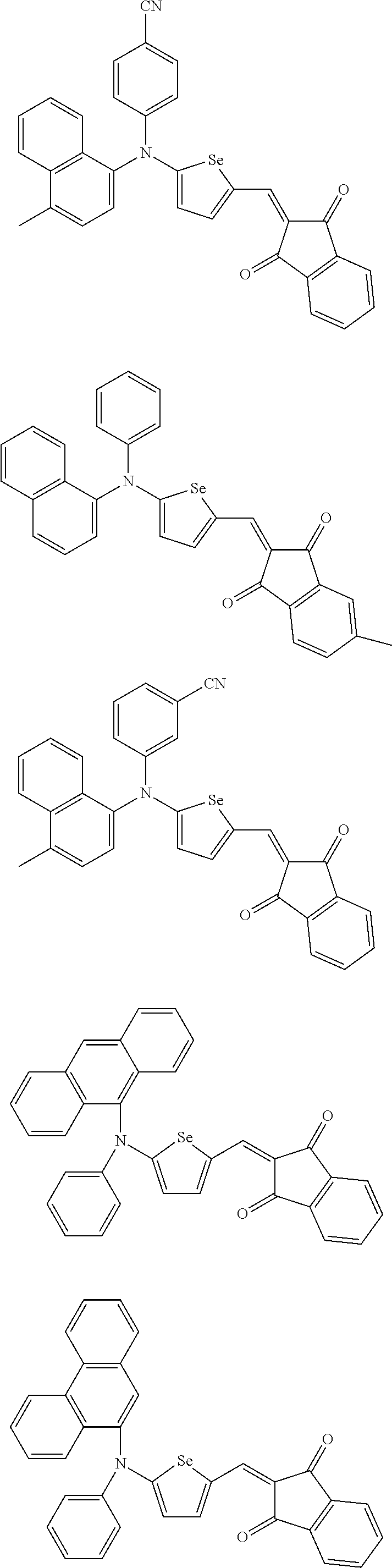


The first light absorbing material may include, for example a compound represented by one of Chemical Formulae 2B-1 to 2B-4.

In Chemical Formulae 2B-1 to 2B-4,
- X is Se, Te, SO, SO2, or SiRaRb,
- Z1 is O or CRcRd,
- Y1 is N or CRe,
- Y2 is selected from O, S, Se, Te, and C(Rf)(CN),
- Y3 is O, S, Se, or Te,
- Y4 is N or NR18a,
- Y5 is CR19a or C═CR20a(CN),
- Ar1a and Area are independently a substituted or unsubstituted C6 to C30 aryl group or a substituted or unsubstituted C3 to C30 heteroaryl group,
- G1 is selected from a single bond, —(CRgRh)n2—, —O—, —S—, —Se—, —N═, —NRi—, —SiRjRk—, and —GeRlRm—, wherein n2 is 1 or 2,
- R1a to R3a, R11a, R12a, R15a to R20a, R24a, R25a, and Ra to Rm are independently hydrogen, a substituted or unsubstituted C1 to C30 alkyl group, a substituted or unsubstituted C6 to C30 aryl group, a substituted or unsubstituted C3 to C30 heteroaryl group, a substituted or unsubstituted C1 to C6 alkoxy group, a halogen, or a cyano group,
- n1 is 0 or 1, n2 is 0, 1, or 2, m1 is 0 or 1, and m2 is an integer that is inclusively between 0 and 4.
The compound represented by one of Chemical Formulae 2B-1 to 2B-4 may be, for example compounds of Group 2, but is not limited thereto.


In Group 2,
- hydrogen of each aromatic ring may be replaced by a substituent selected from a substituted or unsubstituted C1 to C30 alkyl group, a substituted or unsubstituted C1 to C30 alkoxy group, a substituted or unsubstituted C6 to C30 aryl group, a substituted or unsubstituted C4 to C30 heteroaryl group, a halogen, a cyano group, a cyano-containing group, and a combination thereof, and
- each of R16, R17, R18, R20, and Rf are independently hydrogen, a substituted or unsubstituted C1 to C30 alkyl group, a substituted or unsubstituted C1 to C30 alkoxy group, a substituted or unsubstituted C6 to C30 aryl group, a substituted or unsubstituted C4 to C30 heteroaryl group, a halogen, a cyano group, a cyano-containing group, or a combination thereof.
A thickness of the second buffer layer 42 may range from about 1 nm to about 20 nm.
The organic photoelectronic device 100 may further include an anti-reflection layer (not shown) on one side of the first electrode 10 or the second electrode 20.
The anti-reflection layer is disposed on a light incidence side, decreases reflectance of incident light, and improves light absorbance. In some example embodiments, when light enters through the first electrode 10, the anti-reflection layer may be disposed on one side of the first electrode 10, while when light enters at the second electrode 20, the anti-reflection layer may be disposed on one side of the second electrode 20.
The anti-reflection layer may include, for example, a material having a refractive index of about 1.6 to about 2.5, for example, at least one of a metal oxide, a metal sulfide, and an organic material that have a refractive index within the range. The anti-reflection layer may include, for example, a metal oxide including an aluminum-containing oxide, a molybdenum-containing oxide, a tungsten-containing oxide, a vanadium-containing oxide, a rhenium-containing oxide, a niobium-containing oxide, a tantalum-containing oxide, a titanium-containing oxide, a nickel-containing oxide, a copper-containing oxide, a cobalt-containing oxide, a manganese-containing oxide, a chromium-containing oxide, a tellurium-containing oxide, or a combination thereof, a metal sulfide including a zinc sulfide, or an organic material including an amine derivative, but is not limited thereto.
In this way, the first buffer layer 41 including a charge buffer material is included between the first electrode 10 and the photoelectronic conversion layer 30 and thus may improve charge mobility, and in addition, the second buffer layer 42 including the same material as included photoelectronic conversion layer 30 is further included between the photoelectronic conversion layer 30 and the first buffer layer 41 and thus may reduce heterogeneity on the interface between the photoelectronic conversion layer 30 and the first buffer layer 41 and prevent and/or reduce hindrance of charge movement or charge loss due to a recombination of charges on the interface. Accordingly, efficiency of an organic photoelectronic device may be improved, but its driving voltage and leakage current may be lowered.
Referring to FIG. 2 , an organic photoelectronic device 200 according to some example embodiments includes a first electrode 10 and a second electrode 20 facing each other, a photoelectronic conversion layer 30 between the first electrode 10 and the second electrode 20, and a buffer layer 40 between the first electrode 10 and the photoelectronic conversion layer 30, like the above embodiment. As described above, the photoelectronic conversion layer 30 includes the first light absorbing material and the second light absorbing material.
However, the organic photoelectronic device 200 according to some example embodiments includes a single layer of a buffer layer 40, unlike the above embodiment, and the buffer layer 40 includes a mixture of a non-absorbing material associated with a visible wavelength spectrum of light that is a charge buffer material and the same material as the material of the photoelectronic conversion layer 30.
In some example embodiments, the buffer layer 40 may include a mixture of the non-absorbing material associated with a visible wavelength spectrum of light and the first light absorbing material. For example, the buffer layer 40 may include a mixture of the non-absorbing material associated with a visible wavelength spectrum of light and the first light absorbing material selectively absorbing one of red light, green light, and blue light. In some example embodiments, the buffer layer 40 may include a mixture of the non-absorbing material associated with a visible wavelength spectrum of light and the first light absorbing material selectively absorbing green light having a maximum absorption wavelength (λmax) in about 520 nm to about 580 nm. For example, the buffer layer 40 may include a mixture of the non-absorbing material associated with a visible wavelength spectrum of light represented by Chemical Formula 1A or 1B and the first light absorbing material represented by Chemical Formula 2. In some example embodiments, the buffer layer 40 may include a mixture of the non-absorbing material associated with a visible wavelength spectrum of light represented by Chemical Formula 1A-1, 1B-1, 1A-1a, or 1B-1a and the first light absorbing material represented by one of Chemical Formulae 2A, 2B, 2A-1 to 2A-4, and 2B-1 to 2B-4.
The buffer layer 40 may include the non-absorbing material associated with a visible wavelength spectrum of light and the first light absorbing material in a composition ratio of about 1:99 to about 99:1, for example about 10:90 to about 90:10, about 20:80 to about 80:20, about 30:70 to about 70:30, about 40:60 to about 60:40, or about 50:50. Herein, the composition ratio may be a volume ratio.
The buffer layer 40 may have a thickness of about 2 nm to about 40 nm.
Referring to FIG. 3 , an organic photoelectronic device 300 according to some example embodiments includes a first electrode 10 and a second electrode 20 facing each other, a photoelectronic conversion layer 30 between the first electrode 10 and the second electrode 20, and a buffer layer 40 between the first electrode 10 and the photoelectronic conversion layer 30, like the above embodiment. As described above, the photoelectronic conversion layer 30 includes the first light absorbing material and the second light absorbing material.
However, the buffer layer 40 includes a third buffer layer 43 being adjacent to the first electrode 10 and including the non-absorbing material associated with a visible wavelength spectrum of light and a fourth buffer layer 44 being adjacent to the photoelectronic conversion layer 30 and including a mixture of the first light absorbing material and the non-absorbing material associated with a visible wavelength spectrum of light, unlike the above embodiment.
The third buffer layer 43 may be substantially equivalent (e.g., identical within manufacturing and/or material tolerances) to the first buffer layer 41.
The fourth buffer layer 44 may include a mixture of the non-absorbing material associated with a visible wavelength spectrum of light that is a charge buffer material and the first light absorbing material selectively absorbing one of red light, green light, and blue light. In some example embodiments, the fourth buffer layer 44 may include a mixture of the non-absorbing material associated with a visible wavelength spectrum of light that is a charge buffer material and the first light absorbing material selectively absorbing green light having a maximum absorption wavelength (λmax) in about 520 nm to about 580 nm. For example, the fourth buffer layer 44 may include a mixture of the non-absorbing material associated with a visible wavelength spectrum of light represented by Chemical Formula 1A or 1B and the first light absorbing material represented by Chemical Formula 2. In some example embodiments, the fourth buffer layer 44 may include a mixture of the non-absorbing material associated with a visible wavelength spectrum of light represented by Chemical Formula 1A-1, 1B-1, 1A-1a, or 1B-1a and the first light absorbing material represented by one of Chemical Formulae 2A, 2B, 2A-1 to 2A-4, and 2B-1 to 2B-4.
The buffer layer 40 may have a thickness of about 2 nm to about 40 nm. For example, the third buffer layer 43 may have a thickness of about 1 nm to about 20 nm and the fourth buffer layer 44 may have a thickness of about 1 nm to about 20 nm.
Referring to FIG. 4 , an organic photoelectronic device 400 according to some example embodiments includes a first electrode 10 and a second electrode 20 facing each other, a photoelectronic conversion layer 30 between the first electrode 10 and the second electrode 20, and a buffer layer 40 between the first electrode 10 and the photoelectronic conversion layer 30, like the above embodiment. As described above, the photoelectronic conversion layer 30 includes the first light absorbing material and the second light absorbing material.
In some example embodiments, the buffer layer 40 includes a fifth buffer layer 45 that is adjacent to the first electrode 10 and includes the non-absorbing material associated with a visible wavelength spectrum of light, a sixth buffer layer 47 that is adjacent to the photoelectronic conversion layer 30 and including the first light absorbing material, and a seventh buffer layer 46 between the fifth buffer layer 45 and the sixth buffer layer 47 and that includes a mixture of the first light absorbing material and the non-absorbing material associated with a visible wavelength spectrum of light.
The fifth buffer layer 45 may be substantially equivalent to the first buffer layer 41.
The sixth buffer layer 47 may be substantially equivalent to the second buffer layer 42.
The seventh buffer layer 46 may include a mixture of the non-absorbing material associated with a visible wavelength spectrum of light that is a charge buffer material and the first light absorbing material configured to selectively absorb one of red light, green light, and blue light. In some example embodiments, the seventh buffer layer 46 may include a mixture of the non-absorbing material associated with a visible wavelength spectrum of light that is a charge buffer material and the first light absorbing material configured to selectively absorb green light having a maximum absorption wavelength (λmax) of about 520 nm to about 580 nm. In some example embodiments, the seventh buffer layer 46 may include a mixture of the non-absorbing material associated with a visible wavelength spectrum of light represented by Chemical Formula 1A or 1B and the first light absorbing material represented by Chemical Formula 2. In some example embodiments, the seventh buffer layer 46 may include a mixture of the non-absorbing material associated with a visible wavelength spectrum of light represented by Chemical Formula 1A-1, 1B-1, 1A-1a, or 1B-1a and the first light absorbing material represented by one of Chemical Formulae 2A, 2B, 2A-1 to 2A-4, and 2B-1 to 2B-4.
The seventh buffer layer 46 is positioned between the fifth buffer layer 45 and the sixth buffer layer 47 and includes both a non-absorbing material associated with a visible wavelength spectrum of light included in the fifth buffer layer 45 and a first light absorbing material included in the sixth buffer layer 47 and accordingly, may be configured to further reduce heterogeneity on the interface of each layer from the photoelectronic conversion layer 30 to the first electrode 10 and thus more effectively prevent and/or reduce hindrance of charge movement or charge loss due to a recombination of charges. Accordingly, efficiency of an organic photoelectronic device may be improved, and its driving voltage and leakage current may be further effectively lowered.
The organic photoelectronic device may be applied to a solar cell, an image sensor, a photo-detector, a photo-sensor, and an organic light emitting diode (OLED), but is not limited thereto.
The organic photoelectronic device may be, for example, applied to an image sensor.
Hereinafter, an example of an image sensor including the organic photoelectronic device is described referring to drawings. As an example of an image sensor, an organic CMOS image sensor is described.
Referring to FIGS. 5 and 6 , an organic CMOS image sensor 500 according to some example embodiments includes a semiconductor substrate 110 integrated with photo-sensing devices 50 a and 50 b, a transmission transistor (not shown) and a charge storage 55, a lower insulation layer 60, a color filter layer 70, an upper insulation layer 80, and an organic photoelectronic device 100.
The semiconductor substrate 110 may be a silicon substrate. The semiconductor substrate 110 is integrated with the photo-sensing devices 50 a and 50 b, the transmission transistor 92, and the charge storage 55. One or more of the photo-sensing devices 50 a and 50 b may be a photodiode.
The photo-sensing devices 50 a and 50 b, the transmission transistor 92, and/or the charge storage 55 may be integrated in each pixel, and as shown in the drawings, the photo-sensing devices 50 a and 50 b may be included in each blue pixel and red pixel, while the charge storage 55 may be included in a green pixel.
The photo-sensing devices 50 a and 50 b sense light, the information sensed by the photo-sensing devices may be transferred by the transmission transistor, the charge storage 55 is electrically connected with the organic photoelectronic device 100 that will be described later, and the information of the charge storage 55 may be transferred by the transmission transistor.
A metal wire 62 and a pad 64 are formed on the semiconductor substrate 110. In order to decrease signal delay, the metal wire and pad may at least partially comprise a metal having low resistivity, for example, aluminum (Al), copper (Cu), silver (Ag), and alloys thereof, but is not limited thereto. In some example embodiments, the metal wire 62 and pad 64 may be positioned under the photo-sensing devices 50 a and 50 b.
The lower insulation layer 60 may be formed on the metal wire 62 and the pad 64. The lower insulation layer 60 may at least partially comprise an inorganic insulating material including a silicon oxide and/or a silicon nitride, or a low dielectric constant (low K) material including SiC, SiCOH, SiCO, and SiOF. The lower insulation layer 60 may include a trench 85 exposing the charge storage 55. The trench 85 may be filled with fillers.
The color filter layer 70 is formed on the lower insulation layer 60. The color filter layer 70 includes a first color filter and a second color filter. In the example embodiments illustrated in FIG. 6 , the first color filter is a blue color filter 70B formed in the blue pixel and the second color filter is a red color filter 70R formed in the red pixel. In some example embodiments, one or more of the color filters 70 may be a green color filter 70G.
The upper insulation layer 80 is formed on the color filter layer 70. The upper insulation layer 80 eliminates a step caused by the color filter layer 70 and smoothens the surface 80 a. The upper insulation layer 80 and lower insulation layer 60 may include a contact hole (not shown) exposing a pad, and a through-hole 85 exposing the charge storage 55 of a green pixel.
The organic photoelectronic device 100 is formed on the upper insulation layer 80. The organic photoelectronic device 100 includes the first electrode 10, the buffer layer 40, the photoelectronic conversion layer 30, and the second electrode 20 as described above. The first electrode 10, the buffer layer 40, the photoelectronic conversion layer 30, and the second electrode 20 are sequentially stacked in the example embodiments shown in FIG. 6 , but the present disclosure is not limited thereto, and the second electrode 20, the photoelectronic conversion layer 30, the buffer layer 40, and the first electrode 10 may be disposed in the order shown in FIG. 6 .
The first electrode 10 and the second electrode 20 may be transparent electrodes, and the photoelectronic conversion layer 30 and the buffer layer 40 may be the same as described above with reference to FIGS. 1A-1B and FIG. 2 . The photoelectronic conversion layer 30 may selectively absorb light in a green wavelength spectrum of light, and thus replace a color filter of a green pixel.
When light enters from the second electrode 20, the light in a green wavelength spectrum of light may be mainly absorbed in the photoelectronic conversion layer 30 and photoelectrically converted, while the light in a remainder of the wavelength spectra passes through the buffer layer 40 and the first electrode 10 and may be sensed in the photo-sensing devices 50 a and 50 b.
A focusing lens 96 may be further formed on the organic photoelectronic device 100. The focusing lens 96 may control a direction of incident light 98 and gather the light in one region. The focusing lens 96 may have a shape of, for example, a cylinder or a hemisphere, but is not limited thereto.
As described above, the organic photoelectronic device 100 has a stacked structure and thus may reduce the size of an image sensor and realize a down-sized image sensor.
In FIG. 6 , the organic photoelectronic device of FIG. 1A has a stacked structure, but the organic photoelectronic devices of FIGS. 2 to 4 may be also stacked in the same manner.
In some example embodiments, an organic photoelectronic device configured to selectively absorb light in a green wavelength spectrum of light may be stacked, but the present disclosure is not limited thereto, and may include a structure in which an organic photoelectronic device configured to selectively absorb light in a blue wavelength spectrum of light is stacked and a green photo-sensing device and a red photo-sensing device are integrated in the semiconductor substrate 110, or a structure in which an organic photoelectronic device configured to selectively absorb light in a red wavelength spectrum of light is stacked and a green photo-sensing device and a blue photo-sensing device are integrated in the semiconductor substrate 110.
An organic CMOS image sensor 600 according to some example embodiments includes a semiconductor substrate 110 integrated with photo-sensing devices 50 a and 50 b, a transmission transistor 92, and a charge storage 55, an upper insulation layer 80, and an organic photoelectronic device 100.
However, the organic CMOS image sensor 600 according to some example embodiments includes photo-sensing devices 50 a and 50 b stacked in a perpendicular direction and does not include a color filter layer 70. The photo-sensing devices 50 a and 50 b are electrically connected with the charge storage 55, and may be transferred by the transmission transistor. The photo-sensing devices 50 a and 50 b may selectively absorb light in each wavelength spectrum of light depending on a stack depth.
A focusing lens (not shown) may be further formed on the organic photoelectronic device 100. The focusing lens may control a direction of incident light and gather the light in one region. The focusing lens may have a shape of, for example, a cylinder or a hemisphere, but is not limited thereto.
The organic photoelectronic device configured to selectively absorb light in a green wavelength region is stacked as described above, and the red and blue photo-sensing devices are also stacked, which may reduce the size of an image sensor and realize a down-sized image sensor.
In FIG. 7 , the organic photoelectronic device of FIG. 1A is stacked, but the organic photoelectronic devices of FIGS. 2 to 4 may be also stacked in the same manner.
In FIG. 7 , an organic photoelectronic device configured to selectively absorb light in a green wavelength spectrum of light is stacked, but the present disclosure is not limited thereto, and may include a structure in which an organic photoelectronic device configured to selectively absorb light in a blue wavelength spectrum of light is stacked and a green photo-sensing device and a red photo-sensing device are integrated in the semiconductor substrate 110, or a structure in which an organic photoelectronic device configured to selectively absorb light in a red wavelength spectrum of light is stacked and a green photo-sensing device and a blue photo-sensing device are integrated in the semiconductor substrate 110.
An organic CMOS image sensor 700 according to some example embodiments includes a green photoelectronic device configured to selectively absorb light in a green wavelength spectrum of light, a blue photoelectronic device configured to selectively absorb light in a blue wavelength spectrum of light, and a red photoelectronic device configured to selectively absorb light in a green wavelength spectrum of light, and they are stacked.
The organic CMOS image sensor 700 according to some example embodiments includes a semiconductor substrate 110, a lower insulation layer 60, an intermediate insulation layer 70, an upper insulation layer 80, a first organic photoelectronic device 100 a, a second organic photoelectronic device 100 b, and a third organic photoelectronic device 100 c.
The semiconductor substrate 110 may be a silicon substrate, and is integrated with the transmission transistor 92 and the charge storages 55 a, 55 b, and 55 c.
A metal wire 62 and a pad 64 are formed on the semiconductor substrate 110, and the lower insulation layer 60 is formed on the metal wire and the pad.
The first organic photoelectronic device 100 a is formed on the lower insulation layer 60.
The first organic photoelectronic device 100 a includes a first electrode 10 a and a second electrode 20 a facing each other, a photoelectronic conversion layer 30 a between the first electrode 10 a and the second electrode 20 a, and a buffer layer 40 a between the first electrode 10 a and the photoelectronic conversion layer 30 a. The first electrode 10 a, the second electrode 20 a, the photoelectronic conversion layer 30 a, and the buffer layer 40 a are the same as described above, and the photoelectronic conversion layer 30 a may selectively absorb light in one of red, blue, and green wavelength spectra of light. In some example embodiments, the first organic photoelectronic device 100 a may be a red photoelectronic device.
The first electrode 10 a, the buffer layer 40 a, the photoelectronic conversion layer 30 a, and the second electrode 20 a are sequentially stacked in the drawing, but the present disclosure is not limited thereto, and the second electrode 20 a, the photoelectronic conversion layer 30 a, the buffer layer 40 a, and the first electrode 10 a may be disposed in order.
An intermediate insulation layer 70 is formed on the first organic photoelectronic device 100 a.
A second organic photoelectronic device 100 b is formed on the intermediate insulation layer 70.
The second organic photoelectronic device 100 b includes a first electrode 10 b and a second electrode 20 b facing each other, a photoelectronic conversion layer between the first electrode 10 b and the second electrode 20 b, and a buffer layer 40 b between the first electrode 10 b and the photoelectronic conversion layer 30 b. The first electrode 10 b, the second electrode 20 b, the photoelectronic conversion layer 30 b, and the buffer layer 40 b are the same as described above, and the photoelectronic conversion layer 30 b may selectively absorb light in one of red, blue, and green wavelength spectra of light. In some example embodiments, the second organic photoelectronic device 100 b may be a blue photoelectronic device.
The first electrode 10 b, the buffer layer 40 b, the photoelectronic conversion layer 30 b, and the second electrode 20 b are sequentially stacked in the example embodiments illustrated in FIG. 8 , but the present disclosure is not limited thereto, and the second electrode 20 b, the photoelectronic conversion layer 30 b, the buffer layer 40 b, and the first electrode 10 b may be disposed in order.
An intermediate insulation layer 70 is formed on the second organic photoelectronic device 100 b. The lower insulation layer 60, the intermediate insulation layer 70, and the upper insulation layer 80 have a plurality of through- holes 86 a, 86 b, 86 c exposing the charge storages 55 a, 55 b, and 55 c, respectively.
The third organic photoelectronic device 100 c is formed on the upper insulation layer 80. The third organic photoelectronic device 100 c includes a first electrode 10 c and a second electrode 20 c facing each other, a photoelectronic conversion layer 30 c between the first electrode 10 c and the second electrode 20 c, and a buffer layer 40 c between the first electrode 10 c and the photoelectronic conversion layer 30 c. The first electrode 10 c, the second electrode 20 c, the photoelectronic conversion layer 30 c, and the buffer layer 40 c are the same as described above, and the photoelectronic conversion layer 30 c may selectively absorb light in one of red, blue, and green wavelength spectra of light. In some example embodiments, the third organic photoelectronic device 100 c may be a green photoelectronic device.
The first electrode 10 c, the buffer layer 40 c, the photoelectronic conversion layer 30 c, and the second electrode 20 c are sequentially stacked in the example embodiments illustrated in FIG. 8 , but the present disclosure is not limited thereto, and the second electrode 20 c, the photoelectronic conversion layer 30 c, the buffer layer 40 c, and the first electrode 10 c may be disposed on a substrate in a sequential order.
A focusing lens (not shown) may be further formed on the organic photoelectronic device 100 c. The focusing lens may control a direction of incident light and gather the light in one region. The focusing lens may have a shape of, for example, a cylinder or a hemisphere, but is not limited thereto.
In FIG. 9 , the organic photoelectronic device of FIG. 1A is, for example shown as the first organic photoelectronic device 100 a, the second organic photoelectronic device 100 b, and the third organic photoelectronic device 100 c, but organic photoelectronic devices of FIGS. 2 to 4 may be applied in the same manner.
The first organic photoelectronic device 100 a, the second organic photoelectronic device 100 b, and the third organic photoelectronic device 100 c are sequentially stacked in the example embodiments illustrated in FIG. 9 , but the present disclosure is not limited thereto, and the first organic photoelectronic device 100 a, the second organic photoelectronic device 100 b, and the third organic photoelectronic device 100 c may be stacked in various orders.
As described above, the first organic photoelectronic device 100 a, the second organic photoelectronic device 100 b, and the third organic photoelectronic device 100 c absorbing light in different wavelength spectra have a stacked structure and thus may further reduce the size of an image sensor and realize a down-sized image sensor.
The image sensor may be applied to, for example, various electronic devices such as a mobile phone or a digital camera, but is not limited thereto.
Hereinafter, the present disclosure is illustrated in more detail with reference to some example embodiments. However, the present disclosure is not limited thereto.
Manufacture of Organic Photoelectric Device
A 150 nm-thick anode is formed on a glass substrate by sputtering ITO. Subsequently, on the anode, a compound represented by Chemical Formula 1B-1aa (HOMO: 5.73 eV, LUMO: 2.35 eV) is deposited to form a 5 nm-thick lower buffer layer. On the lower buffer layer, a compound represented by Chemical Formula 2A-1a is deposited to form a 5 nm-thick upper buffer layer. Subsequently, a compound represented by Chemical Formula 2A-1a as a p-type semiconductor and C60 as an n-type semiconductor are codeposited to form a 122 nm-thick photoelectronic conversion layer. Herein, the photoelectronic conversion layer includes a 42 nm-thick lower layer formed by depositing the p-type semiconductor and the n-type semiconductor in a volume ratio of 1.1:1, a 70 nm-thick middle layer formed by depositing the p-type semiconductor and the n-type semiconductor in a volume ratio of 1.9:1, and a 10 nm-thick upper layer formed by depositing the p-type semiconductor and the n-type semiconductor in a volume ratio of 1.5:1, which are sequentially formed by changing the ratio of the p-type semiconductor and the n-type semiconductor. Subsequently, on the photoelectronic conversion layer, a 7 nm-thick cathode is formed by sputtering ITO. On the cathode, a 50 nm-thick anti-reflection layer is formed by depositing aluminum oxide (Al2O3), and a glass plate is used for sealing to manufacture an organic photoelectronic device.

A 150 nm-thick anode is formed on a glass substrate by sputtering ITO. Subsequently, on the anode, a compound represented by Chemical Formula 1B-1aa is deposited to form a 5 nm-thick lower buffer layer. On the lower buffer layer, a compound represented by Chemical Formula 2B-3a is deposited to form a 5 nm-thick upper buffer layer. Subsequently, a 130 nm-thick photoelectronic conversion layer is formed by codepositing a compound represented by Chemical Formula 2B-3a as a p-type semiconductor and C60 as an n-type semiconductor in a volume ratio of 1.8:1. On the photoelectronic conversion layer, a 7 nm-thick cathode is formed by sputtering ITO. Subsequently, on the cathode, a 50 nm-thick anti-reflection layer is formed by depositing aluminum oxide (Al2O3), and a glass plate is used for sealing to manufacture an organic photoelectronic device.

An organic photoelectronic device is manufactured according to the same method as Example 2 except for forming a 110 nm-thick photoelectronic conversion layer.
A 150 nm-thick anode is formed on a glass substrate by sputtering ITO. On the anode, a compound represented by Chemical Formula 1B-1aa and a compound represented by Chemical Formula 2B-3a are codeposited to form a 5 nm-thick buffer layer. Subsequently, a 110 nm-thick photoelectronic conversion layer is formed by codepositing a compound represented by Chemical Formula 2B-3a as a p-type semiconductor and C60 as an n-type semiconductor in a volume ratio of 2:1. On the photoelectronic conversion layer, a 7 nm-thick cathode is formed by sputtering ITO. Subsequently, on the cathode, a 50 nm-thick anti-reflection layer is formed by depositing aluminum oxide (Al2O3), and a glass plate is used for sealing to manufacture an organic photoelectronic device.
An organic photoelectronic device is manufactured according to the same method as Example 4 except for codepositing a compound represented by Chemical Formula 1B-1aa and a compound represented by Chemical Formula 2B-3a to form a 10 nm-thick buffer layer.
An organic photoelectronic device is manufactured according to the same method as Example 4 except for codepositing a compound represented by Chemical Formula 1B-1aa and a compound represented by Chemical Formula 2B-3a to form a 20 nm-thick buffer layer.
An organic photoelectronic device is manufactured according to the same method as Example 1 except for forming no upper buffer layer.
An organic photoelectronic device is manufactured according to the same method as Example 2 except for forming no buffer layer.
An organic photoelectronic device is manufactured according to the same method as Example 3 except for forming no buffer layer.
An organic photoelectronic device is manufactured according to the same method as Example 4 except for depositing a compound represented by Chemical Formula 1B-1aa alone to form a 5 nm-thick buffer layer instead of codepositing a compound represented by Chemical Formula 1B-1aa and a compound represented by Chemical Formula 2B-3a.
Evaluation
Evaluation 1
Photoelectric conversion efficiency (EQE), a leakage current, and a driving voltage of the organic photoelectronic devices according to Example 1 and Comparative Example 1 are evaluated.
The photoelectric conversion efficiency (EQE) is evaluated in a method of Incident Photon to Current Efficiency (IPCE) in a wavelength spectrum of light of 400 nm to 720 nm (λmax=570 nm). The leakage current is evaluated as dark current density and detectivity after heat-treating the organic photoelectronic devices at 140° C. for 1 hour, and herein, the dark current density is measured from a current flowing when a −3V reverse bias is applied to them, and the detectivity is expressed as a light dose when a signal is 10 times as much as a noise. The driving voltage is evaluated as a voltage at 70% of the photoelectric conversion efficiency (EQE).
The results are provided in Table 1.
| TABLE 1 | |||
| Driving | |||
| EQE570 nm | Dark current density (h/s/μm2) | voltage | |
| (%) | (before/after heat treatment) | (V) | |
| Example 1 | 67.6 | 42/5 | 3.4 |
| Comparative | 64.4 | 133/9 | 4.5 |
| Example 1 | |||
Referring to Table 1, the organic photoelectronic device according to Example 1 shows all improved external quantum efficiency (EQE), dark current density, and driving voltage compared with the organic photoelectronic device according to Comparative Example 1.
Evaluation 2
Photoelectric conversion efficiency (EQE), leakage current, and driving voltage of the organic photoelectronic devices according to Examples 2 and 3 and Comparative Examples 2 and 3 are evaluated.
The results are provided in Tables 2 and 3.
| TABLE 2 | |||
| Dark current density (h/s/μm2) | Driving | ||
| EQE535 nm | (before heat treatment/ | voltage | |
| (%) | after heat treatment) | (V) | |
| Example 2 | 72.1 | 138/11 | 2.5 |
| Comparative | 70.6 | 229/14 | 3.0 |
| Example 2 | |||
| TABLE 3 | |||
| Driving | |||
| EQE535 nm | Dark current density (h/s/μm2) | voltage | |
| (%) | (after heat treatment) | (V) | |
| Example 3 | 68.0 | 15 | 4 V |
| Comparative | 66.8 | 21 | 5 V |
| Example 3 | |||
Referring to Table 2, the organic photoelectronic device according to Example 2 shows all improved external quantum efficiency (EQE), dark current density, and driving voltage compared with the organic photoelectronic device according to Comparative Example 2.
Likewise, referring to Table 3, the organic photoelectronic device according to Example 3 shows all improved external quantum efficiency (EQE), dark current density, and driving voltage compared with the organic photoelectronic device according to Comparative Example 3.
Evaluation 3
Photoelectric conversion efficiency (EQE), leakage current, and driving voltage of the organic photoelectronic devices according to Examples 4 to 6 and Comparative Example 4 are evaluated.
The results are provided in Table 4.
| TABLE 4 | ||||
| Driving | ||||
| EQE | Dark current density (h/s/μm2) | voltage | λmax | |
| (%) | (after heat treatment) | (V) | (nm) | |
| Example 4 | 65.7 | 2 | 5 | 535 |
| Example 5 | 64.7 | 1 | 7 | 545 |
| Example 6 | 65.6 | 21 | 6 | 545 |
| Comparative | 61.2 | 21 | |
540 |
| Example 4 | ||||
Referring to Table 4, the organic photoelectronic devices according to Examples 4 to 6 show all improved external quantum efficiency (EQE), dark current density, and driving voltage compared with the organic photoelectronic device according to Comparative Example 4.
Referring to FIG. 10 , the electronic device 1000 includes a memory 1020, a processor 1030, a device 1040, and a communication interface 1050. The device 1040 may include any of the organic photoelectronic devices illustrated and described herein, including the example embodiments of organic photoelectronic device 100 shown in FIGS. 1A-B , the example embodiments of organic photoelectronic device 200 shown in FIG. 2 , the example embodiments of organic photoelectronic device 300 shown in FIG. 3 , and the example embodiments of organic photoelectronic device 400 shown in FIG. 4 . The device 1040 may include any of the organic CMOS image sensors illustrated and described herein, including any of the example embodiments of organic CMOS image sensor 500 shown in FIGS. 5-6 , organic CMOS image sensor 600 shown in FIG. 7 , and the organic CMOS image sensor 700 shown in FIGS. 8-9 .
The electronic device 1000 may be included in one or more various electronic devices, including, for example, a mobile phone, a digital camera, a sensor device, a biosensor device, and the like. In some example embodiments, the electronic device 1000 may include one or more of an image providing server, a mobile device, a computing device, an image outputting device, and an image capturing device. A mobile device may include a mobile phone, a smartphone, a personal digital assistant (PDA), some combination thereof, or the like. A computing device may include a personal computer (PC), a tablet computer, a laptop computer, a netbook, some combination thereof, or the like. An image outputting device may include a TV, a smart TV, some combination thereof, or the like. An image capturing device may include a camera, a camcorder, some combination thereof, or the like.
The memory 1020, the processor 1030, the device 1040, and the communication interface 1050 may communicate with one another through a bus 1010.
The communication interface 1050 may communicate data from an external device using various Internet protocols. For example, the communication interface 1050 may communicate sensor data generated by the device 1040 to an external device. The external device may include, for example, an image providing server, a display device, a mobile device such as, a mobile phone, a smartphone, a personal digital assistant (PDA), a tablet computer, and a laptop computer, a computing device such as a personal computer (PC), a tablet PC, and a netbook, an image outputting device such as a TV and a smart TV, and an image capturing device such as a camera and a camcorder.
The processor 1030 may execute a program and control the electronic device 1000. A program code to be executed by the processor 1030 may be stored in the memory 1020. An electronic system may be connected to an external device through an input/output device (not shown) and exchange data with the external device.
The memory 1020 may store information output from the device 1040, including information transmitted from the transistor 92. The memory 1020 may be a volatile or a nonvolatile memory. The memory 1020 may be a non-transitory computer readable storage medium. The memory may store computer-readable instructions that, when executed, cause the execution of one or more methods, functions, processes, etc. as described herein. In some example embodiments, the processor 1030 may execute one or more of the computer-readable instructions stored at the memory 1020.
In some example embodiments, the electronic device 1000 may include a display panel 1060 that may output an image generated based at least in part upon information output from the device 1040.
In some example embodiments, element 1060 may be absent from the electronic device 1000. In some example embodiments, the communication interface 1050 may include a USB and/or HDMI interface. In some example embodiments, the communication interface 1050 may include a wireless communication interface.
A substrate (not shown) may be positioned at the first electrode 1102 or the second electrode 1110, and may include a light-transmitting material. The light-transmitting material may include, for example, an inorganic material (e.g., glass), or an organic material (e.g., polycarbonate, polymethylmethacrylate, polyethylene terephthalate, polyethylene naphthalate, polyamide, polyethersulfone, or a combination thereof).
One of the first electrode 1102 and the second electrode 1110 is an anode and the other is a cathode. At least one of the first electrode 1102 and second electrode 1110 may be a light-transmitting electrode, and light may enter toward the light-transmitting electrode. The light-transmitting electrode may be made of, for example, a conductive oxide (e.g., indium tin oxide (ITO)), indium doped zinc oxide (IZO), tin oxide (SnO2), aluminum-doped zinc oxide (AZO), and/or gallium-doped zinc oxide (GZO), or a transparent conductor of a conductive carbon composite (e.g., carbon nanotubes (CNT) or graphenes). At least one of the first electrode 1102 and the second electrode 1110 may be an opaque electrode, which may be made of an opaque conductor, for example, aluminum (Al), silver (Ag), gold (Au), and/or lithium (Li).
The solar cell 1100 may include an organic photoelectronic device according to some example embodiments.
First and second auxiliary layers 1104 and 1108 may be positioned between the first electrode 1102 and the photoactive layer 1106 and between the second electrode 1110 and the photoactive layer 1106, respectively. The first and second auxiliary layers 1104 and 1108 may increase charge mobility between the first electrode 1102 and the photoactive layer 1106 and between the second electrode 1110 and the photoactive layer 1106. The first and second auxiliary layers 1104 and 1106 may be at least one selected from, for example, an electron injection layer (EIL), an electron transport layer, a hole injection layer (HIL), a hole transport layer, and a hole blocking layer, but are not limited thereto. One or both of the first and second auxiliary layers 1104 and 1108 may be omitted.
The photoactive layer 1106 may have a tandem structure where at least two thereof are stacked.
Referring to FIG. 12 , a first electrode 1203 a and a second electrode 1203 b are positioned on a substrate 1201, a first emission layer 1205 a is positioned on the first electrode 1203 a, and a second emission layer 1205 b is positioned under the second electrode 1203 b.
The substrate 1201 may include a material selected from the group consisting of glass, quartz, silicon, a synthetic resin, a metal, and a combination thereof. The synthetic resin may include polyethylene naphthalate (PEN), polyethylene terephthalate (PET), polycarbonate, polyvinyl alcohol, polyacrylate, polyimide, polynorbornene and/or polyethersulfone (PES), etc. The metal plate may include a stainless steel foil and/or an aluminum foil, etc.
The first electrode 1203 a may include a material having a work function of about 4.3 eV to about 5.0 eV, about 4.3 eV to about 4.7 eV, or about 4.3 eV to about 4.5 eV. According to example embodiments, the material may include aluminum (Al), copper (Cu), magnesium (Mg), molybdenum (Mo) and/or an alloy thereof, etc. In addition, these metals may be laminated to provide a first electrode. The first electrode 1203 a may have a thickness of about 120 to about 120 nm.
The second electrode 1203 b may include a material having a work function of about 12.3 eV to about 12.7 eV or about 12.5 eV to about 12.7 eV. According to some example embodiments, the second electrode 1203 b may include Ba:Al. The second electrode 1203 b may have a thickness of about 120 to about 120 nm.
The organic light-emitting display apparatus 1200 may include an organic photoelectronic device according to some example embodiments.
A middle electrode 1209 is positioned between the first emission layer 1205 a and the second emission layer 1205 b. The middle electrode 1209 may include a material having a work function of about 5.0 eV to about 5.2 eV. According to some example embodiments, the material may include a conductive polymer. The conductive polymer may include polythiophene, polyaniline, polypyrrole, polyacene, polyphenylene, polyphenylenevinylene, a derivative thereof, a copolymer thereof, or a mixture thereof.
A buffer layer 1207 may be positioned between the first emission layer 1205 a and the middle electrode 1209, and may include a material selected from the group consisting of a metal oxide, a polyelectrolyte, and combinations thereof. The combination thereof refers to the metal oxide and polyelectrolyte being mixed or laminated to provide a multi-layer. In addition, the different kinds of metal oxide or polyelectrolyte may be laminated.
Referring to FIG. 13 , a sensor 1300 (for example a gas sensor, light sensor, energy sensor, but example embodiments are not limited thereto) includes at least one electrode 1320 configured to output a signal to a processor 1330. The processor 1330 may include a microprocessor, but example embodiments are not limited thereto. The sensor 1300 may include an organic photoelectronic device according to some example embodiments.
It should be understood that example embodiments described herein should be considered in a descriptive sense only and not for purposes of limitation. Descriptions of features or aspects within each device or method according to example embodiments should typically be considered as available for other similar features or aspects in other devices or methods according to example embodiments. While some example embodiments have been particularly shown and described, it will be understood by one of ordinary skill in the art that variations in form and detail may be made therein without departing from the spirit and scope of the claims.
Claims (28)
1. An organic photoelectronic device, comprising:
a first electrode;
a second electrode on the first electrode;
a photoelectronic conversion layer between the first electrode and the second electrode, the photoelectronic conversion layer including a p-n junction, the p-n junction including a first light absorbing material and a second light absorbing material, the first light absorbing material including an organic material; and
a buffer layer between the first electrode and the photoelectronic conversion layer, the buffer layer including the first light absorbing material and a non-absorbing organic material associated with a visible wavelength spectrum of light, the non-absorbing organic material having a highest occupied molecular orbital (HOMO) energy level of about 5.4 eV to about 5.8 eV,
wherein the buffer layer includes
a first buffer layer that is adjacent to the first electrode and includes the non-absorbing organic material associated with the visible wavelength spectrum of light, and
a second buffer layer that is adjacent to the photoelectronic conversion layer and includes the first light absorbing material.
2. The organic photoelectronic device of claim 1 , wherein the first light absorbing material is configured to selectively absorb light within one of a red wavelength spectrum of light, a green wavelength spectrum of light, and a blue wavelength spectrum of light.
3. The organic photoelectronic device of claim 1 , wherein the first light absorbing material is configured to selectively absorb a green wavelength spectrum of light having a maximum absorption wavelength (λmax) of about 520 nm to about 580 nm.
4. The organic photoelectronic device of claim 1 , wherein the photoelectronic conversion layer and the buffer layer are in contact with each other.
5. The organic photoelectronic device of claim 1 , wherein
the second buffer layer further includes the non-absorbing organic material associated with the visible wavelength spectrum of light.
6. The organic photoelectronic device of claim 1 , wherein the buffer layer further includes,
a third buffer layer that is between the first buffer layer and the second buffer layer and includes a mixture of the first light absorbing material and the non-absorbing organic material associated with the visible wavelength spectrum of light.
7. The organic photoelectronic device of claim 1 , wherein the non-absorbing organic material associated with the visible wavelength spectrum of light is a compound represented by Chemical Formula 1A or 1B,

wherein, in Chemical Formula 1A or 1B,
each of M1 and M2 are independently CRnRo, SiRpRq, NRr, O, S, Se, or Te,
each of Ar1b, Ar2b, Ar3b, and Ar4b are independently a substituted or unsubstituted C6 to C30 aryl group or a substituted or unsubstituted C3 to C30 heteroaryl group,
each of G2 and G3 are independently a single bond, —(CRaRt)n3—, —O—, —S—, —Se—, —N═, —NRu—, —SiRvRw— or —GeRxRy—, wherein n3 is 1 or 2, and
each of R30 to R37 and Rn to Ry are independently hydrogen, a substituted or unsubstituted C1 to C30 alkyl group, a substituted or unsubstituted C6 to C30 aryl group, a substituted or unsubstituted C3 to C30 heterocyclic group, a substituted or unsubstituted C1 to C6 alkoxy group, a halogen, or a cyano group.
8. The organic photoelectronic device of claim 1 , wherein the first light absorbing material has a core structure including an electron donating moiety, a pi-conjugation linker, and an electron accepting moiety.
9. The organic photoelectronic device of claim 8 , wherein the first light absorbing material is a compound represented by Chemical Formula 2,

wherein, in Chemical Formula 2,
X is Se, Te, SO, SO2, or SiRaRb,
EDG is an electron donating group,
EAG is an electron accepting group, and
each of R1, R2, Ra, and Rb are independently hydrogen or a monovalent substituent.
10. The organic photoelectronic device of claim 9 , wherein the first light absorbing material is a compound represented by Chemical Formula 2A or 2B,

wherein, in Chemical Formula 2A or 2B,
X is Se, Te, SO, SO2, or SiRaRb,
Ar is a substituted or unsubstituted 5-membered ring, a substituted or unsubstituted 6-membered ring, or a fused ring of two or more rings,
each of Aria and Ar2a are independently a substituted or unsubstituted C6 to C30 aryl group or a substituted or unsubstituted C3 to C30 heteroaryl group,
each of Ar1a and Ar2a are independently present or are linked to each other to provide a ring,
G1 is selected from a single bond, —(CRgRh)n2—, —O—, —S—, —Se—, —N═, —SiRjRk—, and —GeRlRm—, wherein n2 is 1 or 2, and
each of R1a to R3a, Ra, and Rb are independently hydrogen, a substituted or unsubstituted C1 to C30 alkyl group, a substituted or unsubstituted C6 to C30 aryl group, a substituted or unsubstituted C3 to C30 heteroaryl group, a substituted or unsubstituted C1 to C6 alkoxy group, a halogen, or a cyano group.
11. The organic photoelectronic device of claim 10 , wherein the first light absorbing material is a compound represented by one of Chemical Formulae 2A-1 to 2A-4,

wherein, in Chemical Formulae 2A-1 to 2A-4,
X is Se, Te, SO, SO2, or SiRaRb,
Z1 is O or CRcRd,
Y1 is N or CRe,
Y2 is selected from O, S, Se, Te, and C(Rf)(CN),
Y3 is O, S, Se, or Te,
Y4 is N or NR18a,
Y5 is CR19a or C═CR20a(CN),
each of Ar1a and Ar2a are independently a substituted or unsubstituted C6 to C30 aryl group or a substituted or unsubstituted C3 to C30 heteroaryl group,
each of R1a to R3a, R11a, R12a, R15a to R20a, R24a, R25a, and Ra to Rf are independently hydrogen, a substituted or unsubstituted C1 to C30 alkyl group, a substituted or unsubstituted C6 to C30 aryl group, a substituted or unsubstituted C3 to C30 heteroaryl group, a substituted or unsubstituted C1 to C6 alkoxy group, a halogen, or a cyano group,
n1 is 0 or 1,
m1 is 0 or 1, and
m2 is an integer inclusively between 0 and 4.
12. The organic photoelectronic device of claim 10 , wherein the first light absorbing material is a compound represented by one of Chemical Formulae 2B-1 to 2B-4,

wherein, in Chemical Formulae 2B-1 to 2B-4,
X is Se, Te, SO, SO2, or SiRaRb,
Z1 is O or CRcRd,
Y1 is N or CRe,
Y2 is selected from O, S, Se, Te, and C(Rf)(CN),
Y3 is O, S, Se, or Te,
Y4 is N or NR18a,
Y5 is CR19a or C═CR20a(CN),
each of Aria and Area are independently a substituted or unsubstituted C6 to C30 aryl group or a substituted or unsubstituted C3 to C30 heteroaryl group,
G1 is selected from —(CRgRh)n2—, —O—, —S—, —Se—, —N═, —NRi—, —SiRjRk—, and —GeRlRm—, and
each of R1a to R3a, R11a, R12a, R15a to R20a, R24a, R25a, and Ra to Rm are independently hydrogen, a substituted or unsubstituted C1 to C30 alkyl group, a substituted or unsubstituted C6 to C30 aryl group, a substituted or unsubstituted C3 to C30 heteroaryl group, a substituted or unsubstituted C1 to C6 alkoxy group, a halogen,
or a cyano group,
n1 is 0 or 1,
n2 is 0, 1, or 2,
m1 is 0 or 1, and
m2 is an integer inclusively between 0 and 4.
13. The organic photoelectronic device of claim 1 , wherein,
the photoelectronic conversion layer includes an intrinsic layer, the intrinsic layer including,
a first region that is proximate to the first electrode,
a second region that is proximate to the second electrode, and
a third region that is between the first region and the second region in a thickness direction,
the first region includes a first composition ratio of the first light absorbing material relative to the second light absorbing material,
the second region includes a second composition ratio of the first light absorbing material relative to the second light absorbing material,
the third region includes a third composition ratio of the first light absorbing material relative to the second light absorbing material, and
the third composition ratio is different from each of the first composition ratio and the second composition ratio.
14. The organic photoelectronic device of claim 13 , wherein,
the first light absorbing material is configured to selectively absorb a green wavelength spectrum of light having a maximum absorption wavelength (λmax) of about 520 nm to about 580 nm, and
the second light absorbing material includes fullerene or a fullerene derivative.
15. The organic photoelectronic device of claim 1 , wherein the buffer layer has a thickness of about 2 nm to about 40 nm.
16. The organic photoelectronic device of claim 1 , wherein the first electrode is an anode and the second electrode is a cathode.
17. An image sensor comprising the photoelectronic device of claim 1 .
18. An electronic device comprising the image sensor of claim 17 .
19. An organic photoelectronic device, comprising:
a first electrode;
a second electrode on the first electrode;
a photoelectronic conversion layer between the first electrode and the second electrode, the photoelectronic conversion layer including a p-n junction, the p-n junction including a first light absorbing material and a second light absorbing material, the first light absorbing material including an organic material; and
a buffer layer between the first electrode and the photoelectronic conversion layer, the buffer layer including the first light absorbing material and a non-absorbing organic material associated with a visible wavelength spectrum of light, the non-absorbing organic material having a highest occupied molecular orbital (HOMO) energy level of about 5.4 eV to about 5.8 eV,
wherein the buffer layer includes a mixture of the first light absorbing material and the non-absorbing organic material associated with the visible wavelength spectrum of light.
20. An image sensor comprising the photoelectronic device of claim 19 .
21. An organic photoelectronic device, comprising:
a first electrode;
a second electrode on the first electrode;
a photoelectronic conversion layer between the first electrode and the second electrode, the photoelectronic conversion layer including a p-n junction, the p-n junction including a first light absorbing material and a second light absorbing material, the first light absorbing material including an organic material; and
a buffer layer between the first electrode and the photoelectronic conversion layer, the buffer layer including the first light absorbing material and a non-absorbing organic material associated with a visible wavelength spectrum of light, the non-absorbing organic material having a highest occupied molecular orbital (HOMO) energy level of about 5.4 eV to about 5.8 eV,
wherein the non-absorbing organic material associated with the visible wavelength spectrum of light is a compound represented by Chemical Formula 1A or 1B,

wherein, in Chemical Formula 1A or 1B,
each of M1 and M2 are independently CRnRo, SiRpRq, NRr, O, S, Se, or Te,
each of Ar1b, Ar2b, Ar3b, and Ar4b are independently a substituted or unsubstituted C6 to C30 aryl group or a substituted or unsubstituted C3 to C30 heteroaryl group,
each of G2 and G3 are independently a single bond, —(CRaRt)n3—, —O—, —S—, —Se—, —N═, —NRu—, —SiRvRw— or —GeRxRy—, wherein n3 is 1 or 2, and
each of R30 to R37 and Rn to Ry are independently hydrogen, a substituted or unsubstituted C1 to C30 alkyl group, a substituted or unsubstituted C6 to C30 aryl group, a substituted or unsubstituted C3 to C30 heterocyclic group, a substituted or unsubstituted C1 to C6 alkoxy group, a halogen, or a cyano group.
22. An image sensor comprising the photoelectronic device of claim 21 .
23. An organic photoelectronic device, comprising:
a first electrode;
a second electrode on the first electrode;
a photoelectronic conversion layer between the first electrode and the second electrode, the photoelectronic conversion layer including a p-n junction, the p-n junction including a first light absorbing material and a second light absorbing material, the first light absorbing material including an organic material; and
a buffer layer between the first electrode and the photoelectronic conversion layer, the buffer layer including the first light absorbing material and a non-absorbing organic material associated with a visible wavelength spectrum of light,
wherein the first light absorbing material has a core structure including an electron donating moiety, a pi-conjugation linker, and an electron accepting moiety, and the non-absorbing organic material has a highest occupied molecular orbital (HOMO) energy level of about 5.4 eV to about 5.8 eV.
24. The organic photoelectronic device of claim 23 , wherein the first light absorbing material is a compound represented by Chemical Formula 2,

wherein, in Chemical Formula 2,
X is Se, Te, SO, SO2, or SiRaRb,
EDG is an electron donating group,
EAG is an electron accepting group, and
each of R1, R2, Ra, and Rb are independently hydrogen or a monovalent substituent.
25. The organic photoelectronic device of claim 24 , wherein the first light absorbing material is a compound represented by Chemical Formula 2A or 2B,

wherein, in Chemical Formula 2A or 2B,
X is Se, Te, SO, SO2, or SiRaRb,
Ar is a substituted or unsubstituted 5-membered ring, a substituted or unsubstituted 6-membered ring, or a fused ring of two or more rings,
each of Ar1a and Ar2a are independently a substituted or unsubstituted C6 to C30 aryl group or a substituted or unsubstituted C3 to C30 heteroaryl group,
each of Ar1a and Ar2a are independently present or are linked to each other to provide a ring,
G1 is selected from a single bond, —(CRgRh)n2—, —O—, —S—, —Se—, —N═, —NRi—, —SiRjRk—, and —GeRlRm—, wherein n2 is 1 or 2, and
each of R1a to R3a, Ra, and Rb are independently hydrogen, a substituted or unsubstituted C1 to C30 alkyl group, a substituted or unsubstituted C6 to C30 aryl group, a substituted or unsubstituted C3 to C30 heteroaryl group, a substituted or unsubstituted C1 to C6 alkoxy group, a halogen, or a cyano group.
26. The organic photoelectronic device of claim 25 , wherein the first light absorbing material is a compound represented by one of Chemical Formulae 2A-1 to 2A-4,

wherein, in Chemical Formulae 2A-1 to 2A-4,
X is Se, Te, SO, SO2, or SiRaRb,
Z1 is O or CRcRd,
Y1 is N or CRe,
Y2 is selected from O, S, Se, Te, and C(Rf)(CN),
Y3 is O, S, Se, or Te,
Y4 is N or NR18a,
Y5 is CR19a or C═CR20a(CN),
each of Ar1a and Ar2a are independently a substituted or unsubstituted C6 to C30 aryl group or a substituted or unsubstituted C3 to C30 heteroaryl group,
each of R1a to R3a, R11a, R12a, R15a to R20a, R24a, R25a, and Ra to Rf are independently hydrogen, a substituted or unsubstituted C1 to C30 alkyl group, a substituted or unsubstituted C6 to C30 aryl group, a substituted or unsubstituted C3 to C30 heteroaryl group, a substituted or unsubstituted C1 to C6 alkoxy group, a halogen, or a cyano group,
n1 is 0 or 1,
m1 is 0 or 1, and
m2 is an integer inclusively between 0 and 4.
27. The organic photoelectronic device of claim 25 , wherein the first light absorbing material is a compound represented by one of Chemical Formulae 2B-1 to 2B-4,

wherein, in Chemical Formulae 2B-1 to 2B-4,
X is Se, Te, SO, SO2, or SiRaRb,
Z1 is O or CRcRd,
Y1 is N or CRe,
Y2 is selected from O, S, Se, Te, and C(Rf)(CN),
Y3 is O, S, Se, or Te,
Y4 is N or NR18a,
Y5 is CR19a or C═CR20a(CN),
each of Ar1a and Ar2a are independently a substituted or unsubstituted C6 to C30 aryl group or a substituted or unsubstituted C3 to C30 heteroaryl group,
G1 is selected from —(CRgRh)n2—, —O—, —S—, —Se—, —N═, —SiRjRk—, and —GeRiRm—, and
each of R1a to R3a, R11a, R12a, R15a to R20a, R24a, R25a, and Ra to Rm are independently hydrogen, a substituted or unsubstituted C1 to C30 alkyl group, a substituted or unsubstituted C6 to C30 aryl group, a substituted or unsubstituted C3 to C30 heteroaryl group, a substituted or unsubstituted C1 to C6 alkoxy group, a halogen, or a cyano group,
n1 is 0 or 1,
n2 is 0, 1, or 2,
m1 is 0 or 1, and
m2 is an integer inclusively between 0 and 4.
28. An image sensor comprising the photoelectronic device of claim 23 .
Priority Applications (1)
| Application Number | Priority Date | Filing Date | Title |
|---|---|---|---|
| US16/258,952 US10615354B2 (en) | 2016-05-20 | 2019-01-28 | Organic photoelectronic device and image sensor |
Applications Claiming Priority (2)
| Application Number | Priority Date | Filing Date | Title |
|---|---|---|---|
| KR20160062362 | 2016-05-20 | ||
| KR10-2016-0062362 | 2016-05-20 |
Related Child Applications (1)
| Application Number | Title | Priority Date | Filing Date |
|---|---|---|---|
| US16/258,952 Division US10615354B2 (en) | 2016-05-20 | 2019-01-28 | Organic photoelectronic device and image sensor |
Publications (2)
| Publication Number | Publication Date |
|---|---|
| US20170338431A1 US20170338431A1 (en) | 2017-11-23 |
| US10236461B2 true US10236461B2 (en) | 2019-03-19 |
Family
ID=57755206
Family Applications (2)
| Application Number | Title | Priority Date | Filing Date |
|---|---|---|---|
| US15/362,964 Active US10236461B2 (en) | 2016-05-20 | 2016-11-29 | Organic photoelectronic device and image sensor |
| US16/258,952 Active US10615354B2 (en) | 2016-05-20 | 2019-01-28 | Organic photoelectronic device and image sensor |
Family Applications After (1)
| Application Number | Title | Priority Date | Filing Date |
|---|---|---|---|
| US16/258,952 Active US10615354B2 (en) | 2016-05-20 | 2019-01-28 | Organic photoelectronic device and image sensor |
Country Status (4)
| Country | Link |
|---|---|
| US (2) | US10236461B2 (en) |
| EP (1) | EP3246961A1 (en) |
| KR (1) | KR102673658B1 (en) |
| CN (1) | CN107403867B (en) |
Cited By (3)
| Publication number | Priority date | Publication date | Assignee | Title |
|---|---|---|---|---|
| US20190207119A1 (en) * | 2016-04-06 | 2019-07-04 | Samsung Electronics Co., Ltd. | Compound and organic photoelectric device, image sensor and electronic device including the same |
| US20220216418A1 (en) * | 2020-12-24 | 2022-07-07 | Samsung Electronics Co., Ltd. | Compound and photoelectric device, image sensor, and electronic device including the same |
| US11557741B2 (en) | 2018-11-14 | 2023-01-17 | Samsung Electronics Co., Ltd. | Photoelectric conversion devices and organic sensors and electronic devices |
Families Citing this family (14)
| Publication number | Priority date | Publication date | Assignee | Title |
|---|---|---|---|---|
| TWI770159B (en) * | 2017-04-21 | 2022-07-11 | 日商索尼股份有限公司 | Imaging element, multilayer imaging element, and solid-state imaging device |
| DE102017111137B4 (en) * | 2017-05-22 | 2025-07-10 | Novaled Gmbh | Organic electroluminescent device |
| WO2019111603A1 (en) | 2017-12-05 | 2019-06-13 | ソニー株式会社 | Imaging element, laminate-type imaging element, and solid-state imaging device |
| FR3076082B1 (en) * | 2017-12-21 | 2020-01-24 | Isorg | IMAGE SENSOR |
| KR102718282B1 (en) * | 2019-01-22 | 2024-10-15 | 삼성전자주식회사 | Photoelectric diode and organic sensor and electronic device |
| CN111490070B (en) * | 2019-04-11 | 2023-02-03 | 广东聚华印刷显示技术有限公司 | Display panel |
| KR102697765B1 (en) * | 2019-05-15 | 2024-08-21 | 삼성전자주식회사 | Fingerprint sensor and fingerprint sensor array and device |
| KR102736229B1 (en) * | 2019-06-14 | 2024-11-28 | 삼성전자주식회사 | Organic sensor and electronic device |
| WO2021006567A1 (en) * | 2019-07-05 | 2021-01-14 | 동우화인켐 주식회사 | Transparent electrode structure and electrical device comprising same |
| KR102819096B1 (en) * | 2019-11-01 | 2025-06-11 | 삼성전자주식회사 | Photoelectric device and sensor and electronic device |
| US11563186B2 (en) | 2019-11-01 | 2023-01-24 | Samsung Electronics Co., Ltd. | Photoelectric devices having charge transport layer including first charge transport material and second charge transport material and sensors and electronic devices having the same |
| US20220255028A1 (en) * | 2021-02-08 | 2022-08-11 | Uif (University Industry Foundation), Yonsei University | Skin-conformable biosignal monitoring sensor by applying organic-inorganic hybrid photo transistor and manufacturing method thereof |
| US12048172B2 (en) * | 2021-09-03 | 2024-07-23 | Visera Technologies Company Limited | Solid-state image sensor |
| CN113566980B (en) * | 2021-09-23 | 2021-12-28 | 西安中科立德红外科技有限公司 | Hybrid Imaging Detector |
Citations (85)
| Publication number | Priority date | Publication date | Assignee | Title |
|---|---|---|---|---|
| EP0529162A1 (en) | 1991-08-27 | 1993-03-03 | Milliken Research Corporation | Colorants and intermediates therefor having branched poly(oxyalkylene)moieties, and their manufacture |
| JPH09311232A (en) | 1996-05-21 | 1997-12-02 | Hitachi Ltd | Optical waveguide, manufacturing method thereof, and optical module |
| JPH1091384A (en) | 1996-09-19 | 1998-04-10 | Hokkaido Nippon Denki Software Kk | Display system for tool bar |
| US6087258A (en) | 1994-06-06 | 2000-07-11 | International Business Machines Corporation | Method for circuitizing through-holes by photo-activated seeding |
| US6300612B1 (en) | 1998-02-02 | 2001-10-09 | Uniax Corporation | Image sensors made from organic semiconductors |
| WO2002064600A1 (en) | 2001-02-09 | 2002-08-22 | Siemens Aktiengesellschaft | Amorphous organic 1,3,2-dioxaborine luminophores, method for the production and use thereof |
| DE102004014046A1 (en) | 2003-03-19 | 2004-09-30 | Technische Universität Dresden | Photoactive device with organic layers |
| US6824952B1 (en) | 2001-09-13 | 2004-11-30 | Microchem Corp. | Deep-UV anti-reflective resist compositions |
| JP2005132914A (en) | 2003-10-29 | 2005-05-26 | Mitsubishi Paper Mills Ltd | Photoelectric conversion material, semiconductor electrode, and photoelectric conversion element using the same |
| US20050217722A1 (en) | 2004-03-31 | 2005-10-06 | Takahiro Komatsu | Organic photoelectric conversion element and method of producing the same, organic photodiode and image sensor using the same, organic diode and method of producing the same |
| US6972431B2 (en) | 2003-11-26 | 2005-12-06 | Trustees Of Princeton University | Multilayer organic photodetectors with improved performance |
| JP2006261172A (en) | 2005-03-15 | 2006-09-28 | Matsushita Electric Ind Co Ltd | Organic photodiode and image sensor using the same |
| US7129466B2 (en) | 2002-05-08 | 2006-10-31 | Canon Kabushiki Kaisha | Color image pickup device and color light-receiving device |
| US7141863B1 (en) | 2002-11-27 | 2006-11-28 | University Of Toledo | Method of making diode structures |
| US20070012955A1 (en) | 2005-06-29 | 2007-01-18 | Fuji Photo Film Co., Ltd. | Organic and inorganic hybrid photoelectric conversion device |
| US20070063156A1 (en) | 2005-09-20 | 2007-03-22 | Fuji Photo Film Co., Ltd. | Organic photoelectric conversion element and image element |
| JP2007234650A (en) | 2006-02-27 | 2007-09-13 | Fujifilm Corp | Photoelectric conversion device and solid-state imaging device |
| WO2008019167A2 (en) | 2006-03-10 | 2008-02-14 | Amo Manufacturing Usa, Llc | Output energy control for lasers |
| JP2009274966A (en) | 2008-05-13 | 2009-11-26 | Toyobo Co Ltd | Method for producing diaryloxybiphenyltetracarboxylic dianhydride |
| WO2010011658A2 (en) | 2008-07-21 | 2010-01-28 | The Johns Hopkins University | Pyromellitic diimide organic semiconductors and devices |
| WO2010038721A1 (en) | 2008-09-30 | 2010-04-08 | コニカミノルタホールディングス株式会社 | Organic photoelectric conversion element and method for manufacturing the same |
| US20100207112A1 (en) | 2007-09-28 | 2010-08-19 | Fuerst Jens | Organic photodetector having a reduced dark current |
| US20110012091A1 (en) | 2009-01-12 | 2011-01-20 | The Regents Of The University Of Michigan | Enhancement of organic photovoltaic cell open circuit voltage using electron/hole blocking exciton blocking layers |
| US20110074491A1 (en) | 2009-09-29 | 2011-03-31 | Fujifilm Corporation | Photoelectric conversion device, photoelectric conversion device material, photosensor and imaging device |
| US7973307B2 (en) | 2006-05-25 | 2011-07-05 | The Trustees Of Princeton University | Organic photosensitive devices using subphthalocyanine compounds |
| US8035708B2 (en) | 2007-04-06 | 2011-10-11 | Sony Corporation | Solid-state imaging device with an organic photoelectric conversion film and imaging apparatus |
| JP2011225544A (en) | 2010-03-31 | 2011-11-10 | Fujifilm Corp | New compound, electron-blocking material and film |
| JP2011253861A (en) | 2010-05-31 | 2011-12-15 | Fujifilm Corp | Photoelectric conversion element, image pickup device, and method for driving photoelectric conversion element |
| US20120126204A1 (en) | 2010-11-23 | 2012-05-24 | Nanoholdings, Llc | Ir photodetectors with high detectivity at low drive voltage |
| JP2012123292A (en) | 2010-12-10 | 2012-06-28 | Konica Minolta Advanced Layers Inc | Optical film, and polarizing plate and liquid crystal display device using the same |
| JP2012151761A (en) | 2011-01-20 | 2012-08-09 | Nitto Denko Corp | Surface protection adhesive tape for solid-state imaging device |
| US20120266958A1 (en) * | 2008-11-07 | 2012-10-25 | Solopower, Inc. | Methods of forming ruthenium-group iiia alloys |
| US20120313088A1 (en) | 2010-02-25 | 2012-12-13 | Fujifilm Corporation | Photoelectric conversion device, imaging device and production methods thereof |
| US8378339B2 (en) | 2009-09-11 | 2013-02-19 | Fujifilm Corporation | Photoelectric conversion device, production method thereof, photosensor, imaging device and their drive methods |
| JP2013040147A (en) | 2011-08-19 | 2013-02-28 | Kuraray Co Ltd | Metal complex and adsorbing material, storing material, separating material comprising the same |
| US20130062595A1 (en) | 2011-09-09 | 2013-03-14 | Samsung Electronics Co., Ltd. | Photodiode |
| US8426727B2 (en) | 2005-03-04 | 2013-04-23 | Heliatek Gmbh | Organic photoactive device |
| US8471246B2 (en) | 2008-10-15 | 2013-06-25 | Fujifilm Corporation | Photoelectric conversion device and imaging device |
| US20130181202A1 (en) | 2010-09-08 | 2013-07-18 | Fujifilm Corporation | Photoelectric conversion material, film containing the material, photoelectric conversion device, method for preparing photoelectric conversion device, method for using photoelectric conversion device, photosensor and imaging device |
| JP5323025B2 (en) | 2010-10-26 | 2013-10-23 | 富士フイルム株式会社 | Solid-state image sensor |
| US20140008619A1 (en) * | 2012-07-06 | 2014-01-09 | Samsung Electronics Co., Ltd. | Organic photoelectric material and organic photoelectric device and image sensor |
| US20140054442A1 (en) * | 2012-07-20 | 2014-02-27 | Board Of Regents Of The University Of Nebraska | Nanocomposite Photodetector |
| JP2014049559A (en) | 2012-08-30 | 2014-03-17 | Konica Minolta Inc | Tandem photoelectric conversion element and solar cell using the same |
| US20140083496A1 (en) * | 2012-09-26 | 2014-03-27 | Kabushiki Kaisha Toshiba | Photoelectric conversion element and solar cell |
| US8704281B2 (en) | 2009-08-28 | 2014-04-22 | Fujifilm Corporation | Process of making a solid state imaging device |
| US20140159752A1 (en) * | 2012-12-07 | 2014-06-12 | Tsmc Solar Ltd. | Rapid analysis of buffer layer thickness for thin film solar cells |
| US20140209173A1 (en) | 2011-10-20 | 2014-07-31 | Fujitsu Limited | Photoelectric conversion device and method for producing the same |
| KR20140106767A (en) | 2013-02-22 | 2014-09-04 | 삼성전자주식회사 | Photoelectronic device and image sensor |
| US8847208B2 (en) | 2009-06-03 | 2014-09-30 | Fujifilm Corporation | Photoelectric conversion device and imaging device having decreased dark current |
| US8847141B2 (en) | 2009-06-03 | 2014-09-30 | Fujifilm Corporation | Photoelectric conversion element, production method thereof, photosensor, imaging device and their driving method |
| WO2014157238A1 (en) | 2013-03-28 | 2014-10-02 | 富士フイルム株式会社 | Photoelectric conversion material, photoelectric conversion element and method for using same, optical sensor, and image pickup element |
| US8860016B2 (en) | 2010-03-31 | 2014-10-14 | Fujifilm Corporation | Photoelectric conversion device and imaging device |
| WO2014169270A2 (en) | 2013-04-12 | 2014-10-16 | The Regents Of The University Of Michigan | Organic photosensitive devices with exciton-blocking charge carrier filters |
| US20140319509A1 (en) * | 2011-11-15 | 2014-10-30 | Konica Minolta, Inc. | Organic photoelectric conversion element, and solar cell and optical sensor array each using same |
| JP2014210768A (en) | 2013-04-01 | 2014-11-13 | 株式会社パーマケム・アジア | Electron transport material and electronic material using the electron transport material |
| CN104230953A (en) | 2014-08-25 | 2014-12-24 | 中国科学院上海有机化学研究所 | Naphthalene diimide containing 2-(1,3-dithio/seleno-2-subunit)ethylcyanide conjugate structure unit and derivatives thereof |
| US8933438B2 (en) | 2011-10-31 | 2015-01-13 | Samsung Electronics Co., Ltd. | Photodiode |
| JP2015015415A (en) | 2013-07-08 | 2015-01-22 | 富士フイルム株式会社 | Method for forming photoelectric conversion layer |
| US20150053942A1 (en) * | 2013-08-23 | 2015-02-26 | Samsung Display Co., Ltd. | Organic light-emitting device |
| US20150060775A1 (en) | 2013-08-28 | 2015-03-05 | Taiwan Semiconductor Manufacturing Company, Ltd. | Organic photo diode with dual electron blocking layers |
| JP2015043362A (en) | 2013-08-26 | 2015-03-05 | 富士フイルム株式会社 | Photoelectric conversion element and image pickup element |
| US8994132B2 (en) | 2010-09-27 | 2015-03-31 | Fujifilm Corporation | Photoelectric conversion element, solid-sate imaging element, imaging apparatus, and method for manufacturing photoelectric conversion element |
| JP2015070060A (en) | 2013-09-27 | 2015-04-13 | 富士フイルム株式会社 | Photoelectric conversion element and imaging device |
| JP2015092546A (en) | 2013-09-30 | 2015-05-14 | 富士フイルム株式会社 | Photoelectric conversion device and image pickup device |
| US20150162548A1 (en) | 2013-12-06 | 2015-06-11 | Samsung Electronics Co., Ltd. | Organic photoelectronic device and image sensor |
| US20150228811A1 (en) * | 2014-02-12 | 2015-08-13 | Showa Shell Sekiyu K.K. | Compound-based thin film solar cell |
| US20150349073A1 (en) * | 2014-05-29 | 2015-12-03 | SK Hynix Inc. | Dual work function buried gate-type transistor, method for forming the same, and electronic device including the same |
| US20160013424A1 (en) | 2013-03-27 | 2016-01-14 | Fujifilm Corporation | Photoelectric conversion element and method of using same, optical sensor and image sensor |
| US20160013248A1 (en) | 2013-03-29 | 2016-01-14 | Fujifilm Corporation | Photoelectric conversion element and imaging device using the same |
| US20160020258A1 (en) | 2014-07-16 | 2016-01-21 | Samsung Electronics Co., Ltd. | Organic photoelectronic device and image sensor |
| US20160064672A1 (en) | 2014-09-02 | 2016-03-03 | Gwangju Institute Of Science And Technology | Pedot:pss based electrode and method for manufacturing the same |
| KR20160024686A (en) | 2014-08-26 | 2016-03-07 | 삼성전자주식회사 | Organic photoelectronic device and image sensor |
| US20160099417A1 (en) | 2014-10-06 | 2016-04-07 | Samsung Display Co., Ltd. | Organic electroluminescent device |
| US20160111561A1 (en) | 2014-10-15 | 2016-04-21 | Sensortek Technology Corp. | Package structure with optical barrier, optical package structure and manufacturing methods thereof |
| US20160111651A1 (en) | 2014-10-21 | 2016-04-21 | Samsung Electronics Co., Ltd. | Organic photoelectric device, and image sensor and electronic device including the same |
| US20160126470A1 (en) | 2014-11-04 | 2016-05-05 | Samsung Electronics Co., Ltd. | Compound for organic photoelectric device and organic photoelectric device, image sensor, and electronic device including the same |
| US20160149132A1 (en) | 2014-11-25 | 2016-05-26 | Samsung Electronics Co., Ltd. | Compound for organic photoelectric device and organic photoelectric device image sensor, and electronic device including the same |
| US20160197281A1 (en) * | 2013-09-27 | 2016-07-07 | Fujitsu Limited | Photoelectric conversion device and fabrication method therefor |
| US20160268401A1 (en) | 2013-12-26 | 2016-09-15 | Intel Corporation | Complementary tunneling fet devices and method for forming the same |
| US20170005142A1 (en) | 2015-07-03 | 2017-01-05 | Samsung Electronics Co., Ltd. | Organic photoelectronic device and image sensor |
| US9548463B2 (en) | 2014-07-21 | 2017-01-17 | Samsung Electronics Co., Ltd. | Organic photoelectronic device and image sensor |
| US20170074652A1 (en) | 2014-04-22 | 2017-03-16 | Basf Se | Detector for optically detecting at least one object |
| US20170117424A1 (en) * | 2013-04-16 | 2017-04-27 | Solar Frontier K.K. | Solar cell and method for manufacturing solar cell |
| US20170294589A1 (en) | 2016-04-06 | 2017-10-12 | Samsung Electronics Co. , Ltd. | Compound and organic photoelectric device, image sensor and electronic device including the same |
| US9960362B2 (en) | 2016-05-31 | 2018-05-01 | Samsung Electronics Co., Ltd. | Compound and organic photoelectric device, image sensor and electronic device including the same |
Family Cites Families (5)
| Publication number | Priority date | Publication date | Assignee | Title |
|---|---|---|---|---|
| US6555405B2 (en) * | 2001-03-22 | 2003-04-29 | Uni Light Technology, Inc. | Method for forming a semiconductor device having a metal substrate |
| JP5312692B2 (en) * | 2010-07-29 | 2013-10-09 | 京セラ株式会社 | Photoelectric conversion device |
| KR101326970B1 (en) * | 2011-11-29 | 2013-11-13 | 엘지이노텍 주식회사 | Solaa cell and solaa cell module using the same |
| US9331293B2 (en) * | 2013-03-14 | 2016-05-03 | Nutech Ventures | Floating-gate transistor photodetector with light absorbing layer |
| KR102255234B1 (en) * | 2014-04-04 | 2021-05-21 | 삼성전자주식회사 | Organic photoelectronic device and image sensor |
-
2016
- 2016-11-29 US US15/362,964 patent/US10236461B2/en active Active
- 2016-12-05 KR KR1020160164329A patent/KR102673658B1/en active Active
-
2017
- 2017-01-05 EP EP17150423.6A patent/EP3246961A1/en active Pending
- 2017-01-18 CN CN201710037428.7A patent/CN107403867B/en active Active
-
2019
- 2019-01-28 US US16/258,952 patent/US10615354B2/en active Active
Patent Citations (98)
| Publication number | Priority date | Publication date | Assignee | Title |
|---|---|---|---|---|
| EP0529162A1 (en) | 1991-08-27 | 1993-03-03 | Milliken Research Corporation | Colorants and intermediates therefor having branched poly(oxyalkylene)moieties, and their manufacture |
| US6087258A (en) | 1994-06-06 | 2000-07-11 | International Business Machines Corporation | Method for circuitizing through-holes by photo-activated seeding |
| JPH09311232A (en) | 1996-05-21 | 1997-12-02 | Hitachi Ltd | Optical waveguide, manufacturing method thereof, and optical module |
| JPH1091384A (en) | 1996-09-19 | 1998-04-10 | Hokkaido Nippon Denki Software Kk | Display system for tool bar |
| US6300612B1 (en) | 1998-02-02 | 2001-10-09 | Uniax Corporation | Image sensors made from organic semiconductors |
| WO2002064600A1 (en) | 2001-02-09 | 2002-08-22 | Siemens Aktiengesellschaft | Amorphous organic 1,3,2-dioxaborine luminophores, method for the production and use thereof |
| US6824952B1 (en) | 2001-09-13 | 2004-11-30 | Microchem Corp. | Deep-UV anti-reflective resist compositions |
| US7129466B2 (en) | 2002-05-08 | 2006-10-31 | Canon Kabushiki Kaisha | Color image pickup device and color light-receiving device |
| US7141863B1 (en) | 2002-11-27 | 2006-11-28 | University Of Toledo | Method of making diode structures |
| DE102004014046A1 (en) | 2003-03-19 | 2004-09-30 | Technische Universität Dresden | Photoactive device with organic layers |
| US20070090371A1 (en) | 2003-03-19 | 2007-04-26 | Technische Universitaet Dresden | Photoactive component with organic layers |
| JP2005132914A (en) | 2003-10-29 | 2005-05-26 | Mitsubishi Paper Mills Ltd | Photoelectric conversion material, semiconductor electrode, and photoelectric conversion element using the same |
| US6972431B2 (en) | 2003-11-26 | 2005-12-06 | Trustees Of Princeton University | Multilayer organic photodetectors with improved performance |
| US20050217722A1 (en) | 2004-03-31 | 2005-10-06 | Takahiro Komatsu | Organic photoelectric conversion element and method of producing the same, organic photodiode and image sensor using the same, organic diode and method of producing the same |
| US8426727B2 (en) | 2005-03-04 | 2013-04-23 | Heliatek Gmbh | Organic photoactive device |
| JP2006261172A (en) | 2005-03-15 | 2006-09-28 | Matsushita Electric Ind Co Ltd | Organic photodiode and image sensor using the same |
| US20070012955A1 (en) | 2005-06-29 | 2007-01-18 | Fuji Photo Film Co., Ltd. | Organic and inorganic hybrid photoelectric conversion device |
| US20070063156A1 (en) | 2005-09-20 | 2007-03-22 | Fuji Photo Film Co., Ltd. | Organic photoelectric conversion element and image element |
| JP2007234650A (en) | 2006-02-27 | 2007-09-13 | Fujifilm Corp | Photoelectric conversion device and solid-state imaging device |
| WO2008019167A2 (en) | 2006-03-10 | 2008-02-14 | Amo Manufacturing Usa, Llc | Output energy control for lasers |
| US7973307B2 (en) | 2006-05-25 | 2011-07-05 | The Trustees Of Princeton University | Organic photosensitive devices using subphthalocyanine compounds |
| US8035708B2 (en) | 2007-04-06 | 2011-10-11 | Sony Corporation | Solid-state imaging device with an organic photoelectric conversion film and imaging apparatus |
| US20100207112A1 (en) | 2007-09-28 | 2010-08-19 | Fuerst Jens | Organic photodetector having a reduced dark current |
| JP2009274966A (en) | 2008-05-13 | 2009-11-26 | Toyobo Co Ltd | Method for producing diaryloxybiphenyltetracarboxylic dianhydride |
| WO2010011658A2 (en) | 2008-07-21 | 2010-01-28 | The Johns Hopkins University | Pyromellitic diimide organic semiconductors and devices |
| WO2010038721A1 (en) | 2008-09-30 | 2010-04-08 | コニカミノルタホールディングス株式会社 | Organic photoelectric conversion element and method for manufacturing the same |
| US8471246B2 (en) | 2008-10-15 | 2013-06-25 | Fujifilm Corporation | Photoelectric conversion device and imaging device |
| US20120266958A1 (en) * | 2008-11-07 | 2012-10-25 | Solopower, Inc. | Methods of forming ruthenium-group iiia alloys |
| US20110012091A1 (en) | 2009-01-12 | 2011-01-20 | The Regents Of The University Of Michigan | Enhancement of organic photovoltaic cell open circuit voltage using electron/hole blocking exciton blocking layers |
| US8847141B2 (en) | 2009-06-03 | 2014-09-30 | Fujifilm Corporation | Photoelectric conversion element, production method thereof, photosensor, imaging device and their driving method |
| US8847208B2 (en) | 2009-06-03 | 2014-09-30 | Fujifilm Corporation | Photoelectric conversion device and imaging device having decreased dark current |
| US8704281B2 (en) | 2009-08-28 | 2014-04-22 | Fujifilm Corporation | Process of making a solid state imaging device |
| US8637860B2 (en) | 2009-09-11 | 2014-01-28 | Fujifilm Corporation | Photoelectric conversion device, production method thereof, photosensor, imaging device and their drive methods |
| US8378339B2 (en) | 2009-09-11 | 2013-02-19 | Fujifilm Corporation | Photoelectric conversion device, production method thereof, photosensor, imaging device and their drive methods |
| EP2317582A1 (en) | 2009-09-29 | 2011-05-04 | Fujifilm Corporation | Photoelectric conversion device, photoelectric conversion device material, photosensor and imaging device |
| US8525577B2 (en) | 2009-09-29 | 2013-09-03 | Fujifilm Corporation | Photoelectric conversion device, photoelectric conversion device material, photosensor and imaging device |
| US20110074491A1 (en) | 2009-09-29 | 2011-03-31 | Fujifilm Corporation | Photoelectric conversion device, photoelectric conversion device material, photosensor and imaging device |
| US20120313088A1 (en) | 2010-02-25 | 2012-12-13 | Fujifilm Corporation | Photoelectric conversion device, imaging device and production methods thereof |
| JP2011225544A (en) | 2010-03-31 | 2011-11-10 | Fujifilm Corp | New compound, electron-blocking material and film |
| US8860016B2 (en) | 2010-03-31 | 2014-10-14 | Fujifilm Corporation | Photoelectric conversion device and imaging device |
| US20130087682A1 (en) | 2010-05-31 | 2013-04-11 | Fujifilm Corporation | Photoelectric conversion device, imaging device, and method for driving photoelectric conversion device |
| JP2011253861A (en) | 2010-05-31 | 2011-12-15 | Fujifilm Corp | Photoelectric conversion element, image pickup device, and method for driving photoelectric conversion element |
| US20130181202A1 (en) | 2010-09-08 | 2013-07-18 | Fujifilm Corporation | Photoelectric conversion material, film containing the material, photoelectric conversion device, method for preparing photoelectric conversion device, method for using photoelectric conversion device, photosensor and imaging device |
| US8994132B2 (en) | 2010-09-27 | 2015-03-31 | Fujifilm Corporation | Photoelectric conversion element, solid-sate imaging element, imaging apparatus, and method for manufacturing photoelectric conversion element |
| JP5323025B2 (en) | 2010-10-26 | 2013-10-23 | 富士フイルム株式会社 | Solid-state image sensor |
| US8704213B2 (en) | 2010-10-26 | 2014-04-22 | Fujifilm Corporation | Photoelectric conversion device and solid-state imaging |
| US20120126204A1 (en) | 2010-11-23 | 2012-05-24 | Nanoholdings, Llc | Ir photodetectors with high detectivity at low drive voltage |
| JP2012123292A (en) | 2010-12-10 | 2012-06-28 | Konica Minolta Advanced Layers Inc | Optical film, and polarizing plate and liquid crystal display device using the same |
| JP2012151761A (en) | 2011-01-20 | 2012-08-09 | Nitto Denko Corp | Surface protection adhesive tape for solid-state imaging device |
| JP2013040147A (en) | 2011-08-19 | 2013-02-28 | Kuraray Co Ltd | Metal complex and adsorbing material, storing material, separating material comprising the same |
| US20130062595A1 (en) | 2011-09-09 | 2013-03-14 | Samsung Electronics Co., Ltd. | Photodiode |
| US20140209173A1 (en) | 2011-10-20 | 2014-07-31 | Fujitsu Limited | Photoelectric conversion device and method for producing the same |
| US8933438B2 (en) | 2011-10-31 | 2015-01-13 | Samsung Electronics Co., Ltd. | Photodiode |
| US20140319509A1 (en) * | 2011-11-15 | 2014-10-30 | Konica Minolta, Inc. | Organic photoelectric conversion element, and solar cell and optical sensor array each using same |
| US20140008619A1 (en) * | 2012-07-06 | 2014-01-09 | Samsung Electronics Co., Ltd. | Organic photoelectric material and organic photoelectric device and image sensor |
| US20140054442A1 (en) * | 2012-07-20 | 2014-02-27 | Board Of Regents Of The University Of Nebraska | Nanocomposite Photodetector |
| JP2014049559A (en) | 2012-08-30 | 2014-03-17 | Konica Minolta Inc | Tandem photoelectric conversion element and solar cell using the same |
| US20140083496A1 (en) * | 2012-09-26 | 2014-03-27 | Kabushiki Kaisha Toshiba | Photoelectric conversion element and solar cell |
| US20140159752A1 (en) * | 2012-12-07 | 2014-06-12 | Tsmc Solar Ltd. | Rapid analysis of buffer layer thickness for thin film solar cells |
| US9070888B2 (en) | 2013-02-22 | 2015-06-30 | Samsung Electronics Co., Ltd. | Photoelectronic device and image sensor |
| KR20140106767A (en) | 2013-02-22 | 2014-09-04 | 삼성전자주식회사 | Photoelectronic device and image sensor |
| US20160013424A1 (en) | 2013-03-27 | 2016-01-14 | Fujifilm Corporation | Photoelectric conversion element and method of using same, optical sensor and image sensor |
| WO2014157238A1 (en) | 2013-03-28 | 2014-10-02 | 富士フイルム株式会社 | Photoelectric conversion material, photoelectric conversion element and method for using same, optical sensor, and image pickup element |
| US20160013248A1 (en) | 2013-03-29 | 2016-01-14 | Fujifilm Corporation | Photoelectric conversion element and imaging device using the same |
| JP2014210768A (en) | 2013-04-01 | 2014-11-13 | 株式会社パーマケム・アジア | Electron transport material and electronic material using the electron transport material |
| WO2014169270A2 (en) | 2013-04-12 | 2014-10-16 | The Regents Of The University Of Michigan | Organic photosensitive devices with exciton-blocking charge carrier filters |
| US20170117424A1 (en) * | 2013-04-16 | 2017-04-27 | Solar Frontier K.K. | Solar cell and method for manufacturing solar cell |
| JP2015015415A (en) | 2013-07-08 | 2015-01-22 | 富士フイルム株式会社 | Method for forming photoelectric conversion layer |
| US20150053942A1 (en) * | 2013-08-23 | 2015-02-26 | Samsung Display Co., Ltd. | Organic light-emitting device |
| JP2015043362A (en) | 2013-08-26 | 2015-03-05 | 富士フイルム株式会社 | Photoelectric conversion element and image pickup element |
| US20150060775A1 (en) | 2013-08-28 | 2015-03-05 | Taiwan Semiconductor Manufacturing Company, Ltd. | Organic photo diode with dual electron blocking layers |
| JP2015070060A (en) | 2013-09-27 | 2015-04-13 | 富士フイルム株式会社 | Photoelectric conversion element and imaging device |
| US20160197281A1 (en) * | 2013-09-27 | 2016-07-07 | Fujitsu Limited | Photoelectric conversion device and fabrication method therefor |
| JP2015092546A (en) | 2013-09-30 | 2015-05-14 | 富士フイルム株式会社 | Photoelectric conversion device and image pickup device |
| KR20150066616A (en) | 2013-12-06 | 2015-06-17 | 삼성전자주식회사 | Organic photoelectronic device and image sensor |
| US20150162548A1 (en) | 2013-12-06 | 2015-06-11 | Samsung Electronics Co., Ltd. | Organic photoelectronic device and image sensor |
| US20160268401A1 (en) | 2013-12-26 | 2016-09-15 | Intel Corporation | Complementary tunneling fet devices and method for forming the same |
| US20150228811A1 (en) * | 2014-02-12 | 2015-08-13 | Showa Shell Sekiyu K.K. | Compound-based thin film solar cell |
| US20170074652A1 (en) | 2014-04-22 | 2017-03-16 | Basf Se | Detector for optically detecting at least one object |
| US20150349073A1 (en) * | 2014-05-29 | 2015-12-03 | SK Hynix Inc. | Dual work function buried gate-type transistor, method for forming the same, and electronic device including the same |
| US20160020258A1 (en) | 2014-07-16 | 2016-01-21 | Samsung Electronics Co., Ltd. | Organic photoelectronic device and image sensor |
| KR20160009404A (en) | 2014-07-16 | 2016-01-26 | 삼성전자주식회사 | Organic photoelectronic device and image sensor |
| US9548463B2 (en) | 2014-07-21 | 2017-01-17 | Samsung Electronics Co., Ltd. | Organic photoelectronic device and image sensor |
| CN104230953A (en) | 2014-08-25 | 2014-12-24 | 中国科学院上海有机化学研究所 | Naphthalene diimide containing 2-(1,3-dithio/seleno-2-subunit)ethylcyanide conjugate structure unit and derivatives thereof |
| KR20160024686A (en) | 2014-08-26 | 2016-03-07 | 삼성전자주식회사 | Organic photoelectronic device and image sensor |
| US9543361B2 (en) | 2014-08-26 | 2017-01-10 | Samsung Electronics Co., Ltd. | Organic photoelectronic device including a PN junction and image sensor |
| US20160064672A1 (en) | 2014-09-02 | 2016-03-03 | Gwangju Institute Of Science And Technology | Pedot:pss based electrode and method for manufacturing the same |
| US20160099417A1 (en) | 2014-10-06 | 2016-04-07 | Samsung Display Co., Ltd. | Organic electroluminescent device |
| US20160111561A1 (en) | 2014-10-15 | 2016-04-21 | Sensortek Technology Corp. | Package structure with optical barrier, optical package structure and manufacturing methods thereof |
| US20160111651A1 (en) | 2014-10-21 | 2016-04-21 | Samsung Electronics Co., Ltd. | Organic photoelectric device, and image sensor and electronic device including the same |
| KR20160052448A (en) | 2014-11-04 | 2016-05-12 | 삼성전자주식회사 | Compound for organic photoelectric device and organic photoelectric device image sensor, and electronic device including the same |
| US20160126470A1 (en) | 2014-11-04 | 2016-05-05 | Samsung Electronics Co., Ltd. | Compound for organic photoelectric device and organic photoelectric device, image sensor, and electronic device including the same |
| KR20160062708A (en) | 2014-11-25 | 2016-06-02 | 삼성전자주식회사 | Compound for organic photoelectric device and organic photoelectric device, image sensor and electronic device including the same |
| EP3026722A1 (en) | 2014-11-25 | 2016-06-01 | Samsung Electronics Co., Ltd. | Compound for organic photoelectric device and organic photoelectric device, image sensor, and electronic device including the same |
| US20160149132A1 (en) | 2014-11-25 | 2016-05-26 | Samsung Electronics Co., Ltd. | Compound for organic photoelectric device and organic photoelectric device image sensor, and electronic device including the same |
| US20170005142A1 (en) | 2015-07-03 | 2017-01-05 | Samsung Electronics Co., Ltd. | Organic photoelectronic device and image sensor |
| US20170294589A1 (en) | 2016-04-06 | 2017-10-12 | Samsung Electronics Co. , Ltd. | Compound and organic photoelectric device, image sensor and electronic device including the same |
| US9960362B2 (en) | 2016-05-31 | 2018-05-01 | Samsung Electronics Co., Ltd. | Compound and organic photoelectric device, image sensor and electronic device including the same |
Non-Patent Citations (29)
| Title |
|---|
| Advanced Materials (1997), 9(2), 132-135. |
| Drechsel J. et al: "Efficient organic solar cells based on a double p-i-n. architecture using doped wide-gap transport layers", Applied Physics Letters, AIP Publishing LLC, US, vol. 86, No. 24, Jun. 7, 2005 (Jun. 7, 2005), pp. 244102-244102, XP012065900, ISSN: 0003-6951, DOI: 10.1063/1.1935771. |
| DRECHSEL J., MÄNNIG B., KOZLOWSKI F., PFEIFFER M., LEO K., HOPPE H.: "Efficient organic solar cells based on a double p-i-n architecture using doped wide-gap transport layers", APPLIED PHYSICS LETTERS, A I P PUBLISHING LLC, US, vol. 86, no. 24, 7 June 2005 (2005-06-07), US, pages 244102 - 244102, XP012065900, ISSN: 0003-6951, DOI: 10.1063/1.1935771 |
| European Search Report dated Apr. 26, 2017 issued in corresponding European Application No. 16195944.0. |
| European Search Report dated Apr. 26, 2017 issued in corresponding European Application No. 16195944.0-1555. |
| European Search Report for Application No. 17177002.7 dated Nov. 17, 2017. |
| European Search Report issued in corresponding European Patent Application No. 17150423.6-1555 dated Aug. 4, 2017. |
| Extended European Search Report dated May 22, 2017, for corresponding European Patent Application No. 17161078.5. |
| Gorkem Memisoglu et al., "Highly Efficient Organic UV Photodetectors Based on Polyfluorene and Naphthalenediimide Blends: Effect of Thermal Annealing", 2012, International Journal of Photoenergy vol. 2012, Article ID 936075, 11 pages, Hindawi Publishing Corporation. |
| Hokuto Seo et al. "Color Sensors with Three Vertically Stacked Organic Photodetectors". Japanese Journal of Applied Physics vol. 46, No. 49. The Japan Society of Applied Physics. 2007. pp. L1240-L1242. |
| I.G. Hill et al., Organic Electronics, "Metal-dependent charge transfer and chemical interaction at interfaces between 3,4,9,10-perylenetetracarboxylic bisimidazole and gold, silver and magnesium", Department of Electrical Engineering, Princetion Materials Institute, Feb. 2000, pp. 5-13. |
| I.G. Hill et al., Organic Electronics, "Metal-dependent charge transfer and chemical interaction at interfaces between 3,4,9,10-perylenetetracarboxylic bisimidazole and gold, silver and magnesium", vol. 1, Issue 1, Dec. 2000, pp. 5-13. |
| IDW '09, INP 1-4. |
| IEEE Trans. Electron. Dev., 56(11), 2009, 2570. |
| J. Phys. Chem. A 2013, 117, 9259-9265. |
| Jap. J. Appl. Phys. 46(49), 2007, L1240-L1242. |
| Jiri Misek et al., "A Chiral and Colorful Redox Switch: Enhanced p Acidity in Action", 2010, Angew. Chem. Int. Ed. 2010, 49, 7680-7683, Wiley-VCH Verlag GmbH & Co. KGaA, Weinheim. |
| Journal of Synthetic Organic Chemistry, Japan, vol. 63 (2005) No. 9 p. 911-920. |
| Juha Alakarhu. "Image Sensors and Image Quality in Mobile Phones". International Image Sensor Workshop. 2007. pp. 1-4. |
| Marzena Grucela-Zajac et al., "(Photo) physical Properties of New Molecular Glasses End-Capped with Thiophene Rings Composed of Diimide and Imine Units", The Journal of Physical Chemistry, May 21, 2014, pp. 13070-13086, ACS Author Choice. |
| Scientific Reports 5, Article No. 7708 (2015). |
| The Biophysical Society of Japan, vol. 2, pp. 23-34 (2006). |
| U.S. Notice of Allowance dated Dec. 20, 2017 issued in co-pending U.S. Appl. No. 15/609,125. |
| U.S. Office Action dated Aug. 24, 2018 issued in co-pending U.S. Appl. No. 15/461,914. |
| U.S. Office Action dated Aug. 6, 2018 issued in co-pending U.S. Appl. No. 15/623,801. |
| U.S. Office Action dated Feb. 14, 2018 issued in co-pending U.S. Appl. No. 15/272,580. |
| U.S. Office Action dated Jan. 29, 2018 issued in co-pending U.S. Appl. No. 15/255,649. |
| U.S. Office Action dated Jul. 25, 2018 issued in co-pending U.S. Appl. No. 15/272,580. |
| U.S. Office Action dated Jul. 3, 2017 issued in co-pending U.S. Appl. No. 15/255,649. |
Cited By (5)
| Publication number | Priority date | Publication date | Assignee | Title |
|---|---|---|---|---|
| US20190207119A1 (en) * | 2016-04-06 | 2019-07-04 | Samsung Electronics Co., Ltd. | Compound and organic photoelectric device, image sensor and electronic device including the same |
| US10566544B2 (en) * | 2016-04-06 | 2020-02-18 | Samsung Electronics Co., Ltd. | Compound and organic photoelectric device, image sensor and electronic device including the same |
| US11557741B2 (en) | 2018-11-14 | 2023-01-17 | Samsung Electronics Co., Ltd. | Photoelectric conversion devices and organic sensors and electronic devices |
| US20220216418A1 (en) * | 2020-12-24 | 2022-07-07 | Samsung Electronics Co., Ltd. | Compound and photoelectric device, image sensor, and electronic device including the same |
| US12365697B2 (en) * | 2020-12-24 | 2025-07-22 | Samsung Electronics Co., Ltd. | Compound and photoelectric device, image sensor, and electronic device including the same |
Also Published As
| Publication number | Publication date |
|---|---|
| EP3246961A1 (en) | 2017-11-22 |
| CN107403867B (en) | 2022-10-14 |
| US20170338431A1 (en) | 2017-11-23 |
| CN107403867A (en) | 2017-11-28 |
| US10615354B2 (en) | 2020-04-07 |
| KR20170131193A (en) | 2017-11-29 |
| US20190157594A1 (en) | 2019-05-23 |
| KR102673658B1 (en) | 2024-06-10 |
Similar Documents
| Publication | Publication Date | Title |
|---|---|---|
| US10615354B2 (en) | Organic photoelectronic device and image sensor | |
| US10686149B2 (en) | Optoelectronic diodes and electronic devices including same | |
| US11005070B2 (en) | Organic photoelectronic device and image sensor and electronic device | |
| US11532671B2 (en) | Organic photoelectronic device and image sensor | |
| US10381412B2 (en) | Organic photoelectronic device | |
| US10546897B2 (en) | Photoelectric device and image sensor and electronic device | |
| US10403837B2 (en) | Organic photoelectric device and image sensor | |
| US11437438B2 (en) | Photoelectric conversion devices and organic sensors and electronic devices | |
| US11855236B2 (en) | Sensors and electronic devices | |
| US11631819B2 (en) | Photoelectric conversion device, organic sensor and electronic device | |
| US11495761B2 (en) | Photoelectric conversion devices and organic sensors and electronic devices | |
| US11557741B2 (en) | Photoelectric conversion devices and organic sensors and electronic devices |
Legal Events
| Date | Code | Title | Description |
|---|---|---|---|
| AS | Assignment |
Owner name: SAMSUNG ELECTRONICS CO., LTD., KOREA, REPUBLIC OF Free format text: ASSIGNMENT OF ASSIGNORS INTEREST;ASSIGNORS:RO, TAKKYUN;PARK, KYUNG BAE;SATOH, RYUICHI;AND OTHERS;REEL/FRAME:040495/0945 Effective date: 20161116 |
|
| STCF | Information on status: patent grant |
Free format text: PATENTED CASE |
|
| MAFP | Maintenance fee payment |
Free format text: PAYMENT OF MAINTENANCE FEE, 4TH YEAR, LARGE ENTITY (ORIGINAL EVENT CODE: M1551); ENTITY STATUS OF PATENT OWNER: LARGE ENTITY Year of fee payment: 4 |